EP2560065A1 - Power converter - Google Patents
Power converter Download PDFInfo
- Publication number
- EP2560065A1 EP2560065A1 EP11768744A EP11768744A EP2560065A1 EP 2560065 A1 EP2560065 A1 EP 2560065A1 EP 11768744 A EP11768744 A EP 11768744A EP 11768744 A EP11768744 A EP 11768744A EP 2560065 A1 EP2560065 A1 EP 2560065A1
- Authority
- EP
- European Patent Office
- Prior art keywords
- phase sequence
- phase
- current
- negative
- cluster
- Prior art date
- Legal status (The legal status is an assumption and is not a legal conclusion. Google has not performed a legal analysis and makes no representation as to the accuracy of the status listed.)
- Withdrawn
Links
Images

Classifications
-
- H—ELECTRICITY
- H02—GENERATION; CONVERSION OR DISTRIBUTION OF ELECTRIC POWER
- H02J—CIRCUIT ARRANGEMENTS OR SYSTEMS FOR SUPPLYING OR DISTRIBUTING ELECTRIC POWER; SYSTEMS FOR STORING ELECTRIC ENERGY
- H02J3/00—Circuit arrangements for ac mains or ac distribution networks
- H02J3/26—Arrangements for eliminating or reducing asymmetry in polyphase networks
-
- H—ELECTRICITY
- H02—GENERATION; CONVERSION OR DISTRIBUTION OF ELECTRIC POWER
- H02M—APPARATUS FOR CONVERSION BETWEEN AC AND AC, BETWEEN AC AND DC, OR BETWEEN DC AND DC, AND FOR USE WITH MAINS OR SIMILAR POWER SUPPLY SYSTEMS; CONVERSION OF DC OR AC INPUT POWER INTO SURGE OUTPUT POWER; CONTROL OR REGULATION THEREOF
- H02M7/00—Conversion of ac power input into dc power output; Conversion of dc power input into ac power output
- H02M7/42—Conversion of dc power input into ac power output without possibility of reversal
- H02M7/44—Conversion of dc power input into ac power output without possibility of reversal by static converters
- H02M7/48—Conversion of dc power input into ac power output without possibility of reversal by static converters using discharge tubes with control electrode or semiconductor devices with control electrode
- H02M7/483—Converters with outputs that each can have more than two voltages levels
- H02M7/4835—Converters with outputs that each can have more than two voltages levels comprising two or more cells, each including a switchable capacitor, the capacitors having a nominal charge voltage which corresponds to a given fraction of the input voltage, and the capacitors being selectively connected in series to determine the instantaneous output voltage
-
- H—ELECTRICITY
- H02—GENERATION; CONVERSION OR DISTRIBUTION OF ELECTRIC POWER
- H02J—CIRCUIT ARRANGEMENTS OR SYSTEMS FOR SUPPLYING OR DISTRIBUTING ELECTRIC POWER; SYSTEMS FOR STORING ELECTRIC ENERGY
- H02J3/00—Circuit arrangements for ac mains or ac distribution networks
- H02J3/18—Arrangements for adjusting, eliminating or compensating reactive power in networks
- H02J3/1821—Arrangements for adjusting, eliminating or compensating reactive power in networks using shunt compensators
- H02J3/1835—Arrangements for adjusting, eliminating or compensating reactive power in networks using shunt compensators with stepless control
- H02J3/1842—Arrangements for adjusting, eliminating or compensating reactive power in networks using shunt compensators with stepless control wherein at least one reactive element is actively controlled by a bridge converter, e.g. active filters
- H02J3/1857—Arrangements for adjusting, eliminating or compensating reactive power in networks using shunt compensators with stepless control wherein at least one reactive element is actively controlled by a bridge converter, e.g. active filters wherein such bridge converter is a multilevel converter
-
- Y—GENERAL TAGGING OF NEW TECHNOLOGICAL DEVELOPMENTS; GENERAL TAGGING OF CROSS-SECTIONAL TECHNOLOGIES SPANNING OVER SEVERAL SECTIONS OF THE IPC; TECHNICAL SUBJECTS COVERED BY FORMER USPC CROSS-REFERENCE ART COLLECTIONS [XRACs] AND DIGESTS
- Y02—TECHNOLOGIES OR APPLICATIONS FOR MITIGATION OR ADAPTATION AGAINST CLIMATE CHANGE
- Y02E—REDUCTION OF GREENHOUSE GAS [GHG] EMISSIONS, RELATED TO ENERGY GENERATION, TRANSMISSION OR DISTRIBUTION
- Y02E40/00—Technologies for an efficient electrical power generation, transmission or distribution
- Y02E40/20—Active power filtering [APF]
-
- Y—GENERAL TAGGING OF NEW TECHNOLOGICAL DEVELOPMENTS; GENERAL TAGGING OF CROSS-SECTIONAL TECHNOLOGIES SPANNING OVER SEVERAL SECTIONS OF THE IPC; TECHNICAL SUBJECTS COVERED BY FORMER USPC CROSS-REFERENCE ART COLLECTIONS [XRACs] AND DIGESTS
- Y02—TECHNOLOGIES OR APPLICATIONS FOR MITIGATION OR ADAPTATION AGAINST CLIMATE CHANGE
- Y02E—REDUCTION OF GREENHOUSE GAS [GHG] EMISSIONS, RELATED TO ENERGY GENERATION, TRANSMISSION OR DISTRIBUTION
- Y02E40/00—Technologies for an efficient electrical power generation, transmission or distribution
- Y02E40/50—Arrangements for eliminating or reducing asymmetry in polyphase networks
Definitions
- the present invention relates to a power converter, and more particularly to a three-phase power converter formed with three clusters, each of which is a series circuit including one or a plurality of unit cells.
- a cascade multi-level converter is a circuit system that can output voltages equal to or higher than the withstand voltages of switching elements used therein; the switching elements are, for example, insulated gate bipolar transistors (IGBTs) and other switching elements that can be turned on and off in a controlled manner.
- the CMC is formed by star-connecting three series circuits, each of which is formed with a reactor and a cluster, the cluster being a series circuit formed with a plurality of unit cells.
- each unit cell is a single-phase full bridge circuit; it has a plurality of switching elements and a DC capacitor.
- the unit cell turns on and off the switching elements in a controlled manner to output a voltage across the DC capacitor (referred to below as the DC voltage), a voltage with a polarity opposite to the polarity of the DC voltage, or a zero-voltage.
- the output voltage of the cluster (referred to below as the cluster voltage) is the output voltage of the one unit cell included in the cluster or the sum of the output voltages of the plurality of unit cells therein.
- the cluster voltage can have a multi-level waveform. Accordingly, the harmonic component of the cluster voltage can be reduced by increasing the number of unit cells included in each cluster.
- NPL 1 indicates experimental results of a CMC-based static var compensator (referred to below as the CMC-STATCOM), in which a CMC is linked to a power supply system.
- CMC-STATCOM CMC-based static var compensator
- NPL NON-PATENT LITERATURE
- NPL 1 Yoshii, Inoue, Akagi "Transuresu kasukedo PWM STATCOM no chokuryudenatsuseigyoho no kento (Zero-sequence voltage control of a cascade PWM converter with star-configuration)" IEE-SPC and IEE-IEA materials, SPC-07-115/IEA-07-38, pp. 32-36
- One method of suppressing the power supply system voltage from being unbalanced by an unbalanced load is to link a power converter in the vicinity of the unbalanced load and output a negative-phase sequence current having a phase opposite to the phase of the negative-phase sequence current of the unbalanced load.
- NPL 1 discloses results of experiments in which the CMC-STATCOM output only positive-phase sequence reactive currents and does not disclose a circuit system and control method applied to a case in which negative-phase sequence currents are output.
- the present invention provides a solution described below.
- the present invention provides a power converter that has a delta-connected cascade multi-level converter (CMC) linked to a power supply system, the CMC being formed by delta-connecting series circuits, each of which is formed with a reactor and a cluster, the cluster being a series circuit formed with one or a plurality of unit cells.
- CMC cascade multi-level converter
- the present invention provides a power converter that has a function by which a positive-phase sequence reactive current and a negative-phase sequence current caused by an unbalanced load linked to the power converter are substantially compensated by a positive-phase sequence reactive current and a negative-phase sequence current that are simultaneously output by the power converter.
- CMC cascade multi-level converter
- the present invention provides a power converter that has a function by which a voltage across a DC capacitor in each cell is balanced.
- CMC cascade multi-level converter
- the present invention provides a power converter that has a function by which if the phase angle of the positive-phase sequence component included in a voltage of the power supply system is denoted ⁇ 1 and the negative-phase sequence current command value of the power converter or the root-mean-square value of an actual negative-phase sequence current and the phase angle of the current are respectively denoted I2 and ⁇ 2, each cluster flows a circulating current having root-mean-square value 10 and phase angle ⁇ 0, which are represented by the equations below.
- the present invention provides a power converter characterized in that the power converter has a function by which if the root-mean-square value and phase angle of the positive-phase sequence component included in the voltage of the power supply system are respectively denoted V1 and ⁇ 1, the root-mean-square value and phase angle of the negative-phase sequence component included in the voltage of the power supply system are respectively denoted V2 and ⁇ 2, the command value of the current that flows into the cluster or the root-mean-square value of the positive-phase sequence component of an actual current and the phase angle of the positive-phase sequence component are
- the voltage and current of each of the three clusters are made orthogonal in a state in which a positive-phase sequence reactive current and a negative-phase sequence current are flowing simultaneously in each cluster. Accordingly, active electric power does not flow into each cluster.
- a positive-phase sequence reactive current from an unbalanced current and a negative-phase sequence current can be compensated by using a power converter formed with three series circuits, each of which is formed with a reactor and a cluster, the cluster being a series circuit formed with one or a plurality of unit cells.
- a positive-phase sequence reactive current from an unbalanced current and a negative-phase sequence current can be compensated by using a power converter formed with three series circuits, each of which is formed with a reactor and a cluster, the cluster being a series circuit formed with one or a plurality of unit cells.
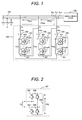
- a power converter 102 connected to a power supply system 101 includes three reactors 103, a uv-phase cluster 104, a vw-phase cluster 105, and a wu-phase cluster 106.
- the uv-, vw-, and wu-phase clusters 104 to 106 may not be distinguished but may be simply referred to as clusters.
- One reactor 103 is connected in series with each of the clusters 104 to 106.
- One end of a series circuit formed with the uv-phase cluster 104 and the reactor 103 is connected to the u-phase of the power supply system, and the other end is connected to the v-phase.
- One end of a series circuit formed with the vw-phase cluster 105 and the reactor 103 is connected to the v-phase of the power supply system, and the other end is connected to the w-phase.
- One end of a series circuit formed with the wu-phase cluster 106 and the reactor 103 is connected to the w-phase of the power supply system, and the other end is connected to the u-phase.
- Each of the clusters 104 to 106 is a series circuit formed with one or a plurality of unit cells 107.
- N unit cells are connected in each cell.
- the unit cells are called a first cell, a second cell, and so on, starting from the unit cell closest to the reactor 103.
- the internal structure of the unit cell 107 will be described later.
- An unbalanced load 108 is connected to the power supply system 101.
- the unbalanced load 108 draws all of a positive-phase sequence active current, a positive-phase sequence reactive current, and a negative-phase sequence current or a combination of these currents from the power supply system 101.
- Phase voltages of the power supply system 101 are denoted VSu, VSv, and VSw.
- a point O is a virtual neutral point at which the sum of VSu, VSv, and VSw becomes 0.
- the line-to-line voltages of the power supply system 101 are denoted VSuv, VSvw, and VSwu.
- Iu Currents that flow from the power supply system 101 into the power converter 102 are denoted Iu, Iv, and Iw.
- Currents that flow into the reactors 103 and the clusters 104 to 106 are denoted Iuv, Ivw, and Iwu.
- Output voltages (cluster voltages) from the clusters 104 to 106 are denoted Vuv, Vvw, and Vwu.
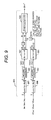
- the unit cell 107 is a single-phase full bridge circuit including an x-phase upper element 201, an x-phase lower element 202, a y-phase upper element 203, a y-phase lower element 204, and a DC capacitor 205.
- the unit cell 107 controls the switching of the elements 201 to 204 to output voltage Vij at a point x, relative to a point y, that is set to 0, VCij, or -VCij.
- the elements 201 to 204 are each represented with a symbol of an IGBT. However, they may be gate turn-off thyristors (GTOs), gate-commutated turn-off thyristors (GCTs), metal-oxide-semiconductor field-effect transistors (MOSFETs), or other types of switching elements that can be tuned on and off in a controlled manner, instead of IGBTs.
- GTOs gate turn-off thyristors
- GCTs gate-commutated turn-off thyristors
- MOSFETs metal-oxide-semiconductor field-effect transistors
- the cluster voltages Vuv, Vvw, and Vwu can be controlled.
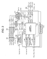
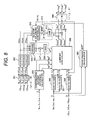
- FIG. 3 shows control blocks, in the controller, that are not shown in FIG. 1 .
- the controller detects line voltages VSuv, VSvw, and VSwu of the power supply system 101 and performs positive-phase sequence dq conversion on these detected line voltages to obtain positive-phase sequence d-axis voltage Vd and positive-phase sequence q-axis voltage Vq.
- the controller also detects currents Iuv, Ivw, and Iwu that flow into the respective reactors and performs positive-phase sequence dq conversion on these detected currents to obtain positive-phase sequence d-axis current Id1 and positive-phase sequence q-axis current Iq1.
- the controller further detects currents Iuv, Ivw, and Iwu that flow into their respective reactors 103 and performs negative-phase sequence dq conversion on these detected currents to obtain negative-phase sequence d-axis current Id2 and negative-phase sequence q-axis current Iq2.
- the controller gives obtained Vd, Vq, Id1, Iq1, Id2, and Iq2 to a current controller 308.
- the current controller calculates cluster voltage commands Vuvcc*, Vvwcc*, and Vwucc* to be output from the current controller so that currents Id1, Iq1, Id2, and Iq2 match their respective command values Id1*, Iq1*, Id2*, and Iq2*.
- Positive-phase sequence d-axis current command value id1* and other current command values Iq1*, Id2*, and Iq2* are given in different methods.
- Positive-phase sequence d-axis current command value id1* is given by a total average DC voltage controller 303.
- Positive-phase sequence q-axis current command value Iq1*, negative-phase sequence d-axis current command value Id2*, and negative-phase sequence q-axis current command value Iq2* are given from currents ILu, ILv, and ILw of the unbalanced load 108 (referred to below as load currents) through a compensating current value calculator 305.
- load currents currents ILu, ILv, and ILw of the unbalanced load 108
- LPF low-pass filter
- An average calculator 302 calculates average DC voltages VCu, VCv, and VCw (referred to below as cluster average DC voltages) in the clusters according to the equations below.
- VCuv VCuvf ⁇ 1 + VCuvf ⁇ 2 + ... + VCuvfN / N
- VCvw VCvwf ⁇ 1 + VCvwf ⁇ 2 + ... + VCvwfN / N
- VCwu VCwuf ⁇ 1 + VCwuf ⁇ 2 + ... + VCwufN / N
- a feedforward calculator 310 uses negative-phase sequence d-axis command value Id2*, negative-phase sequence q-axis command value Iq2*, and system voltages VSuv, VSvw and VSwu to calculate a circulating current command value feedforward term I0FF* by which active electric power that flows into the clusters 104 to 106 and active electric power output from there are made zero.
- a cluster balancing controller 311 uses cluster average DC voltages VCuv, VCvw and VCwu and the total average DC voltage VC to calculate a circulating current command value feedback term I0FB*, which is used in cluster balancing control.
- the cluster balancing controller 311 provides a function that balances the DC voltage of each unit cell.
- the internal structure of the cluster balancing controller 311 will be described later.
- a circulating current controller 312 compares the sum of the circulating current command value feedforward term I0FF* and circulating current command value feedback term I0FB* (I0FF* + I0FB*) with the actual circular current I0 and performs a multiplication by a circulating current control gain 313 to calculate a zero-phase sequence voltage command value V0.
- the circulating current controller 312 further adds cluster voltage command values Vuvcc*, Vvwcc*, and Vwucc* supplied from the current controller to the obtained V0 to obtain cluster voltage command values Vuv*, Vvw*, and Vwu*.
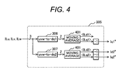
- the internal structure of the compensating current value calculator 305 will be described below with reference to FIG. 4 .
- the compensating current value calculator 305 detects load currents ILu, ILv and ILw and calculates positive-phase sequence d-axis current ⁇ ILd1> and positive-phase sequence q-axis current ⁇ ILq1> through the positive-phase sequence dq converting block and a moving average calculator 401.
- the compensating current value calculator 305 also calculates negative-phase sequence d-axis current ⁇ ILd1> and negative-phase sequence q-axis current ⁇ ILq1> from ILu, ILv, and ILw through the negative-phase sequence dq converting block and the moving average calculator 401.
- the time window of the moving average calculator 401 is a half cycle of the power supply system or its integer multiple.
- Positive-phase sequence q-axis current ⁇ ILq1> of the load changes the amplitude of the system voltage.
- Negative-phase sequence d-axis and q-axis currents ⁇ ILd2> and ⁇ ILq2> of the load increase the imbalance ratio of the system voltage. Accordingly, it is desirable to output currents having phases opposite to the phases of ⁇ ILq1>, ⁇ ILd2>, and ⁇ ILq2> from the power converter 102 to suppress the change in the amplitude of the system voltage and the increase in the imbalance ratio.
- current command values Iq1*, Id2*, and Iq2* of the power converter 102 are given by using the equations below.
- Iq ⁇ 1 * - ⁇ ILq ⁇ 1 >
- Id ⁇ 2 * - ⁇ ILd ⁇ 2 >
- Iq ⁇ 2 * - ⁇ ILq ⁇ 2 >
- the current controller 308 controls actual currents Iq1, Id2, and Iq2 so that they match given current command values Iq1*, Id2*, and Iq2*.
- the internal structure of the feedforward calculator 310 will be described with reference to FIG. 5 .
- the feedforward calculator 310 obtains negative-phase sequence current root-mean-square value I2 and positive-phase sequence current phase angle ⁇ 2 from the absolute value and angle of vector [Id2*, Iq2*] of given current command values Id2* and Iq2* through an orthogonal coordinate-polar coordinate converting block 501.
- the feedforward calculator 310 also uses the positive-phase sequence dq converting block 306 to perform negative-phase sequence dq conversion on phase voltages VSu, VSv, and VSw of the power supply system 101, and calculates a moving average in which a half cycle of the power supply system is handled as a time window through the moving average calculator 401, obtaining positive-phase sequence d-axis voltage ⁇ Vd1> and positive-phase sequence q-axis voltage ⁇ Vq1>.
- the feedforward calculator 310 also obtains positive-phase sequence voltage root-mean-square value V1 and negative-phase sequence voltage phase angle ⁇ 1 from the sizes and amplitudes of vectors [ ⁇ Vd2>, ⁇ Vq2>] through the orthogonal coordinate-polar coordinate converting block 501.
- a sine wave generator 502 generates the circulating current command value feedforward term I0FF* as a sine wave signal having root-mean-square value 10 and phase angle ⁇ 0.
- the feedforward calculator 310 can also use another algorithm if signals that are mathematically equivalent to the equations in [Eq. 7] to [Eq. 10] can be output.
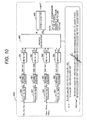
- the internal structure of the cluster balancing controller 311 will be described with reference to FIG. 6 .
- the cluster balancing controller 311 calculates ⁇ VCuv, ⁇ VCvw, and ⁇ VCwu, which are respectively differences between the given total average DC voltage VC and cluster average DC voltages VCuv, VCvw and VCwu.
- the cluster balancing controller 311 then performs ⁇ conversion on the obtained ⁇ VCuv, ⁇ VCvw, and ⁇ VCwu by using an ⁇ converting block 601 and obtains [ ⁇ VC ⁇ , ⁇ VC ⁇ ] as a vector on an ⁇ axis.
- the cluster balancing controller 311 further calculates the sizes ⁇ VC and amplitude ⁇ of vectors [ ⁇ VC ⁇ , ⁇ VC ⁇ ] through an orthogonal coordinate-polar coordinate converting block 602.
- the cluster balancing controller 311 also calculates amplitude ⁇ 1 of vectors [Vd, Vq], that is, the phase angle of the line-to-line voltage between phases u and v of the power supply system, from vectors [Vd, Vq] of given positive-phase sequence d-axis voltage Vd and positive-phase sequence q-axis voltage Vq though the orthogonal coordinate-polar coordinate converting block 501.
- FIG. 7 shows schematic waveforms of each part in a case in which control in the present invention has been carried out.
- the waveforms at the top are schematic waveforms of line-to-line voltages VSuv, VSvw, and VSwu of the power supply system 101, followed by schematic waveforms of currents Iuv, Ivw, and Iwu that flow into the their respective reactors 103 and clusters 104 to 106, a schematic waveform of the circular current (I0FF + I0FB), schematic waveforms of DC voltages VCuvj, VCvwj, and VCwuj, and schematic waveforms of DC voltages VCuvfj, VCvwfj, and VCwufj observed after they have passed through the LPFs 301 in that order.
- the waveforms in FIG. 7 are drawn, assuming that circular current command value 10 ideally follows the command value (I0FF* + I0FB*).
- the horizontal axis indicates time or phase angle
- the vertical axis indicates amplitudes of voltage and current in an arbitrary unit (a.u.).
- the zero-phase sequence feedback term I0FB* plays a role of suppressing the DC voltages from being unbalanced due to variations in the characteristics of parts in use and other factors.
- the clusters 104 to 106 are connected to the power supply system 101 through their respective reactors 103.
- the present invention can also be applied to a case in which the clusters 104 to 106 are each connected to the power supply system 101 through a transformer instead of the reactor 103.
- the present invention can also be applied to a case in which the clusters 104 to 106 are each connected to the power supply system 101 through both the rector 103 and a transformer.
- negative-phase sequence current command values Id2* and Iq2* have been given to the feedforward calculator 310.
- actual negative-phase sequence currents Id2 and Iq2 are given instead of Id2* and Iq2*.
- the feedforward calculator 801 uses a negative-phase sequence dq converting block 307 to perform negative-phase sequence dq conversion on currents Iuv, Ivw, and Iwu, and calculates a moving average in which a half cycle of the power supply system is handled as a time window through the moving average calculator 401, obtaining negative-phase sequence d-axis current ⁇ Id2> and negative-phase sequence q-axis current ⁇ Iq2>.
- the feedforward calculator 801 also obtains root-mean-square value I2 and phase angle ⁇ 2 of the negative-phase sequence current from the sizes and amplitudes of vectors [ ⁇ Id2>, ⁇ Iq2>] through the orthogonal coordinate-polar coordinate converting block 501.
- the feedforward calculator 801 also uses the positive-phase sequence dq converting block 306 to perform negative-phase sequence dq conversion on phase voltages VSu, VSv, and VSw of the power supply system 101, and calculates a moving average in which a half cycle of the power supply system is handled as a time window through the moving average calculator 401, obtaining positive-phase sequence d-axis voltage ⁇ Vd1> and positive-phase sequence q-axis voltage ⁇ Vq1>.
- the feedforward calculator 801 also obtains positive-phase sequence voltage root-mean-square value V1 and negative-phase sequence voltage phase angle ⁇ 1 from the sizes and amplitudes of vectors [ ⁇ Vd2>, ⁇ Vq2>] through the orthogonal coordinate-polar coordinate converting block 501.
- the sine wave generator 502 generates the circulating current command value feedforward term I0FF* as a sine wave signal having root-mean-square value 10 and phase angle ⁇ 0.
- the second embodiment is the same as the first embodiment except the control block ( FIG. 3 ) and feedforward calculator 801, which have been described above.
- the effect that active electric power that flows into the clusters 104 to 106 and active electric power output from there can be made zero can be obtained as in the first and second embodiments.
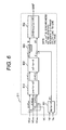
- the third embodiment is characterized in that the feedforward calculator 801, shown in FIG. 9 , in the second embodiment is replaced with a negative-phase sequence voltage ready feedforward calculator 1001 shown in FIG. 10 .
- the negative-phase sequence voltage ready feedforward calculator 1001 obtains positive-phase sequence d-axis current ⁇ Id1> and positive-phase sequence q-axis current ⁇ Iq1> from currents Iuv, Ivw, and Iwu through the positive-phase sequence dq converting block 306 and moving average calculator 401.
- the negative-phase sequence voltage ready feedforward calculator 1001 further obtains positive-phase sequence current root-mean-square value I1 and positive-phase sequence current phase angle ⁇ 1 from the sizes and amplitudes of vectors [ ⁇ Id1>, ⁇ Iq1>] through the orthogonal coordinate-polar coordinate converter 501.
- the negative-phase sequence voltage ready feedforward calculator 1001 obtains negative-phase sequence d-axis current ⁇ Id2> and negative-phase sequence q-axis current ⁇ Iq2> from currents Iu, Iv, and Iw through the negative-phase sequence dq converting block 307 and moving average calculator 401.
- the negative-phase sequence voltage ready feedforward calculator 1001 further obtains negative-phase sequence current root-mean-square value I2 and negative-phase sequence current phase angle ⁇ 2 from the absolute value and angle of vector [ ⁇ Id2>, ⁇ Iq2>] through the orthogonal coordinate-polar coordinate converter 501.
- the negative-phase sequence voltage ready feedforward calculator 1001 obtains positive-phase sequence d-axis voltage ⁇ Vd1> and positive-phase sequence q-axis voltage ⁇ Vq1> from voltages VSuv, VSvw, and VSwu through the positive-phase sequence dq converting block 306 and moving average calculator 401.
- the negative-phase sequence voltage ready feedforward calculator 1001 further obtains positive-phase sequence voltage root-mean-square value V1 and positive-phase sequence voltage phase angle ⁇ 1 from the absolute value and angle of vector [ ⁇ Vd1>, ⁇ Vq1>] through the orthogonal coordinate-polar coordinate converter 501.
- the negative-phase sequence voltage ready feedforward calculator 1001 obtains negative-phase sequence d-axis voltage ⁇ Vd2> and negative-phase sequence q-axis voltage ⁇ Vq2> from voltages VSuv, VSvw, and VSwu through the negative-phase sequence dq converting block 307 and moving average calculator 401.
- the negative-phase sequence voltage ready feedforward calculator 1001 further obtains positive-phase sequence voltage root-mean-square value V2 and positive-phase sequence voltage phase angle ⁇ 2 from the sizes and amplitudes of vector [ ⁇ Vd2>, ⁇ Vq2>] through the orthogonal coordinate-polar coordinate converter 501.
- I ⁇ 0 - I ⁇ 1 ⁇ V ⁇ 2 ⁇ cos ⁇ ⁇ 1 - ⁇ ⁇ 2 + I ⁇ 2 ⁇ V ⁇ 1 ⁇ cos ⁇ ⁇ 2 - ⁇ ⁇ 1 / V ⁇ 1 ⁇ cos ⁇ ⁇ 0 - ⁇ ⁇ 1 + V ⁇ 2 ⁇ cos ⁇ ⁇ 0 - ⁇ ⁇ 2 Eq .
- the negative-phase sequence voltage ready feedforward calculator 1001 can also use another algorithm if signals that are mathematically equivalent to the equations in [Eq. 14] and [Eq. 15] can be output.
- the clusters 104 to 106 are connected to the power supply system 101 through their respective reactors 103.
- the present invention can also be applied to a case in which the clusters 104 to 106 are each connected to the power supply system 101 through a transformer instead of the reactor 103.
- the present invention can also be applied to a case in which the clusters 104 to 106 are each connected to the power supply system 101 through both the rector 103 and a transform.
- LPF low-pass filter
- negative-phase sequence dq converting block 308 ... current controller, 309 ... voltage command value divider, 310 ... feedforward calculator, 311 ... cluster balancing controller, 312 ... circular current controller, 313 ... circular current control gain, 401 ... moving average calculator, 501 ... orthogonal coordinate-polar coordinate converter, 502 ... sine wave generator, 601 ... ⁇ converting block, 602 ... orthogonal coordinate-polar coordinate converting block, 603 ... cluster balancing control gain, 801 ... feedforward calculator that uses actual currents, 1001 ... negative-phase sequence voltage ready feedforward calculator.
Landscapes
- Engineering & Computer Science (AREA)
- Power Engineering (AREA)
- Inverter Devices (AREA)
- Supply And Distribution Of Alternating Current (AREA)
Abstract
In relation to a three-phase power converter that is formed with three clusters, each of which is a serial body including one or a plurality of unit cells, a circuit system and control method used by the three-phase power converter to output negative-phase sequence currents are provided.
In a power converter that has a delta-connected cascade multi-level converter (CMC) linked to a power supply system, the CMC being formed by delta-connecting series circuit, each of which is formed with a reactor and a cluster, the cluster being a serial body formed with one or a plurality of unit cells, a positive-phase sequence reactive current and a negative-phase sequence current caused by an unbalanced load linked to the power supply system are substantially offset by a positive-phase sequence reactive current and a negative-phase sequence current that are simultaneously output by the power converter.
Description
- The present invention relates to a power converter, and more particularly to a three-phase power converter formed with three clusters, each of which is a series circuit including one or a plurality of unit cells.
- A cascade multi-level converter (CMC) is a circuit system that can output voltages equal to or higher than the withstand voltages of switching elements used therein; the switching elements are, for example, insulated gate bipolar transistors (IGBTs) and other switching elements that can be turned on and off in a controlled manner. According to NON-PATENT LITERATURE (NPL) 1, the CMC is formed by star-connecting three series circuits, each of which is formed with a reactor and a cluster, the cluster being a series circuit formed with a plurality of unit cells.
- According to
NPL 1, each unit cell is a single-phase full bridge circuit; it has a plurality of switching elements and a DC capacitor. The unit cell turns on and off the switching elements in a controlled manner to output a voltage across the DC capacitor (referred to below as the DC voltage), a voltage with a polarity opposite to the polarity of the DC voltage, or a zero-voltage. - Since each cluster is a series circuit having one or a plurality of unit cells, the output voltage of the cluster (referred to below as the cluster voltage) is the output voltage of the one unit cell included in the cluster or the sum of the output voltages of the plurality of unit cells therein. When each cluster includes a plurality of unit cells, if the switching timing of each unit cell in the cluster is appropriately shifted, the cluster voltage can have a multi-level waveform. Accordingly, the harmonic component of the cluster voltage can be reduced by increasing the number of unit cells included in each cluster.
- NPL 1 indicates experimental results of a CMC-based static var compensator (referred to below as the CMC-STATCOM), in which a CMC is linked to a power supply system.
- NPL 1: Yoshii, Inoue, Akagi "Transuresu kasukedo PWM STATCOM no chokuryudenatsuseigyoho no kento (Zero-sequence voltage control of a cascade PWM converter with star-configuration)" IEE-SPC and IEE-IEA materials, SPC-07-115/IEA-07-38, pp. 32-36
- When an arc furnace or another unbalanced load is connected to a power supply system, a negative-phase sequence current flowing out of the unbalanced load causes an unbalanced voltage drop in the impedance of the power supply system. As a result, the voltage of a power supply system (referred to below as the power supply system voltage) in the vicinity is unbalanced.
- One method of suppressing the power supply system voltage from being unbalanced by an unbalanced load is to link a power converter in the vicinity of the unbalanced load and output a negative-phase sequence current having a phase opposite to the phase of the negative-phase sequence current of the unbalanced load.
- However,
NPL 1 discloses results of experiments in which the CMC-STATCOM output only positive-phase sequence reactive currents and does not disclose a circuit system and control method applied to a case in which negative-phase sequence currents are output. - When a CMC formed by star-connecting three clusters outputs a negative-phase sequence current, active electric power that flows into each cluster is unbalanced, so the DC voltage of each unit cell included in each cluster is continuously increased or decreased.
- To address the above problem, the present invention provides a solution described below.
- The present invention provides a power converter that has a delta-connected cascade multi-level converter (CMC) linked to a power supply system, the CMC being formed by delta-connecting series circuits, each of which is formed with a reactor and a cluster, the cluster being a series circuit formed with one or a plurality of unit cells.
- In a power converter that has a delta-connected cascade multi-level converter (CMC) linked to a power supply system, the CMC being formed by delta-connecting series circuits, each of which is formed with a reactor and a cluster, the cluster being a series circuit formed with one or a plurality of unit cells, the present invention provides a power converter that has a function by which a positive-phase sequence reactive current and a negative-phase sequence current caused by an unbalanced load linked to the power converter are substantially compensated by a positive-phase sequence reactive current and a negative-phase sequence current that are simultaneously output by the power converter.
- In a power converter that has a delta-connected cascade multi-level converter (CMC) linked to a power supply system, the CMC being formed by delta-connecting series circuits, each of which is formed with a reactor and a cluster, the cluster being a series circuit formed with one or a plurality of unit cells, the present invention provides a power converter that has a function by which a voltage across a DC capacitor in each cell is balanced.
- In a power converter that has a delta-connected cascade multi-level converter (CMC) linked to a power supply system, the CMC being formed by delta-connecting series circuits, each of which is formed with a reactor and a cluster, the cluster being a series circuit formed with one or a plurality of unit cells, the present invention provides a power converter that has a function by which if the phase angle of the positive-phase sequence component included in a voltage of the power supply system is denoted φ1 and the negative-phase sequence current command value of the power converter or the root-mean-square value of an actual negative-phase sequence current and the phase angle of the current are respectively denoted I2 and δ2, each cluster flows a circulating current having root-mean-
square value 10 and phase angle δ0, which are represented by the equations below.

In a power converter that has a delta-connected cascade multi-level converter (CMC) linked to a power supply system, the CMC being formed by delta-connecting series circuits, each of which is formed with a reactor and a cluster, the cluster being a series circuit formed with one or a plurality of unit cells, the present invention provides a power converter characterized in that the power converter has a function by which if the root-mean-square value and phase angle of the positive-phase sequence component included in the voltage of the power supply system are respectively denoted V1 and φ1, the root-mean-square value and phase angle of the negative-phase sequence component included in the voltage of the power supply system are respectively denoted V2 and φ2, the command value of the current that flows into the cluster or the root-mean-square value of the positive-phase sequence component of an actual current and the phase angle of the positive-phase sequence component are respectively denoted I1 and δ1, and the root-mean-square value and phase angle of the negative-phase sequence component of the actual current are respectively denoted I2 and δ2, each cluster outputs a circulating current having root-mean-square value 10 and phase angle δ0, which are substantially represented by the equations below.

In a power converter that has a delta-connected cascade multi-level converter (CMC) linked to a power supply system, the CMC being formed by delta-connecting series circuits, each of which is formed with a reactor and a cluster, the cluster being a series circuit formed with one or a plurality of unit cells, the present invention also provides a power converter characterized in that moving average calculation in which a half cycle of the frequency of the power supply system or its integer multiple is handled as a time window is used in the detection of V1, φ1, V2, φ2, I1, δ1, I2, and δ2. - When the amplitude and phase of the circulating current are controlled as in the present invention, the voltage and current of each of the three clusters are made orthogonal in a state in which a positive-phase sequence reactive current and a negative-phase sequence current are flowing simultaneously in each cluster. Accordingly, active electric power does not flow into each cluster.
- According to the present invention, therefore, a positive-phase sequence reactive current from an unbalanced current and a negative-phase sequence current can be compensated by using a power converter formed with three series circuits, each of which is formed with a reactor and a cluster, the cluster being a series circuit formed with one or a plurality of unit cells.
-
-
FIG. 1 shows is a main circuit diagram of a delta-connected CMC-STATCOM. -
FIG. 2 shows a unit cell of full bridge type. -
FIG. 3 is a control block diagram. -
FIG. 4 shows a compensating current command value calculator. -
FIG. 5 shows a feedforward calculator. -
FIG. 6 shows a cluster balancing controller. -
FIG. 7 shows examples of waveforms in the present invention. -
FIG. 8 shows a negative-phase sequence voltage ready feedforward calculator. -
FIG. 9 is a control block in which actual currents are used. -
FIG. 10 shows a feedforward calculator that uses actual currents. - Embodiments of the present invention will be described below with reference to the drawings.
- A first embodiment of the present invention will be described below.
- In the first embodiment, a positive-phase sequence reactive current from an unbalanced current and a negative-phase sequence current can be compensated by using a power converter formed with three series circuits, each of which is formed with a reactor and a cluster, the cluster being a series circuit formed with one or a plurality of unit cells.
- A whole structure in the first embodiment will be described below with reference to
FIG. 1 . - A
power converter 102 connected to apower supply system 101 includes threereactors 103, a uv-phase cluster 104, a vw-phase cluster 105, and a wu-phase cluster 106. In this description, the uv-, vw-, and wu-phase clusters 104 to 106 may not be distinguished but may be simply referred to as clusters. - One
reactor 103 is connected in series with each of theclusters 104 to 106. One end of a series circuit formed with the uv-phase cluster 104 and thereactor 103 is connected to the u-phase of the power supply system, and the other end is connected to the v-phase. One end of a series circuit formed with the vw-phase cluster 105 and thereactor 103 is connected to the v-phase of the power supply system, and the other end is connected to the w-phase. One end of a series circuit formed with the wu-phase cluster 106 and thereactor 103 is connected to the w-phase of the power supply system, and the other end is connected to the u-phase. - Each of the
clusters 104 to 106 is a series circuit formed with one or a plurality ofunit cells 107. InFIG. 1 , N unit cells are connected in each cell. In theclusters 104 to 106, the unit cells are called a first cell, a second cell, and so on, starting from the unit cell closest to thereactor 103. The internal structure of theunit cell 107 will be described later. - An
unbalanced load 108 is connected to thepower supply system 101. Theunbalanced load 108 draws all of a positive-phase sequence active current, a positive-phase sequence reactive current, and a negative-phase sequence current or a combination of these currents from thepower supply system 101. - Voltages and currents will be defined below.
- Phase voltages of the
power supply system 101 are denoted VSu, VSv, and VSw. A point O is a virtual neutral point at which the sum of VSu, VSv, and VSw becomes 0. The line-to-line voltages of thepower supply system 101 are denoted VSuv, VSvw, and VSwu. - Currents that flow from the
power supply system 101 into thepower converter 102 are denoted Iu, Iv, and Iw. Currents that flow into thereactors 103 and theclusters 104 to 106 are denoted Iuv, Ivw, and Iwu. - Output voltages (cluster voltages) from the
clusters 104 to 106 are denoted Vuv, Vvw, and Vwu. - Furthermore, a DC voltage of the unit cell included in each of the
clusters 104 to 106 is denoted VCij (i = uv, vw, wu). IfN unit cells 107 are included in each cluster, j is 1, 2, ..., or N. - The internal structure of the
unit cell 107 will be described below with reference toFIG. 2. FIG. 2 shows i-phase cell j (i = uv, vw, wu, j = 1, 2, ..., N). - The
unit cell 107 is a single-phase full bridge circuit including an x-phaseupper element 201, an x-phaselower element 202, a y-phaseupper element 203, a y-phaselower element 204, and aDC capacitor 205. Theunit cell 107 controls the switching of theelements 201 to 204 to output voltage Vij at a point x, relative to a point y, that is set to 0, VCij, or -VCij. - In
FIG. 2 , theelements 201 to 204 are each represented with a symbol of an IGBT. However, they may be gate turn-off thyristors (GTOs), gate-commutated turn-off thyristors (GCTs), metal-oxide-semiconductor field-effect transistors (MOSFETs), or other types of switching elements that can be tuned on and off in a controlled manner, instead of IGBTs. - Each of the
clusters 104 to 106 shown inFIG. 1 is a series circuit includingM unit cells 107, as described above. Therefore, each of cluster voltages Vuv, Vvw, and Vwu is the sum of output voltage Vij ofM unit cells 107. These voltages can be represented as Vuv = Vuv1 + Vuv2 + ... + VuvN, Vvw = Vvw1 + Vvw2 + ... + VvwN, and Vwu = Vwu1 + Vwu2 + ... + VwuN. - When the unit cells undergo pulse-width modulation (PWM) control, therefore, the cluster voltages Vuv, Vvw, and Vwu can be controlled.
- Unless otherwise noted, this description will explain the principle and effects of the present invention, focusing on fundamental wave components included in clusters voltages Vuv, Vvw and Vwu and currents Iuv, Ivw and Iwu that flow into the
respective reactors 103 andclusters 104 to 106. - The method of controlling the power converter in the present invention and the principle of the present invention will be described with reference to
FIG. 3 .
FIG. 3 shows control blocks, in the controller, that are not shown inFIG. 1 . - The controller detects line voltages VSuv, VSvw, and VSwu of the
power supply system 101 and performs positive-phase sequence dq conversion on these detected line voltages to obtain positive-phase sequence d-axis voltage Vd and positive-phase sequence q-axis voltage Vq. The controller also detects currents Iuv, Ivw, and Iwu that flow into the respective reactors and performs positive-phase sequence dq conversion on these detected currents to obtain positive-phase sequence d-axis current Id1 and positive-phase sequence q-axis current Iq1. The controller further detects currents Iuv, Ivw, and Iwu that flow into theirrespective reactors 103 and performs negative-phase sequence dq conversion on these detected currents to obtain negative-phase sequence d-axis current Id2 and negative-phase sequence q-axis current Iq2. The controller gives obtained Vd, Vq, Id1, Iq1, Id2, and Iq2 to acurrent controller 308. - In this description, it is assumed that all the reference phase angles of a positive-phase sequence
dq converting block 306 and a negative-phase sequence dq converting block are substantially in synchronization with uv-phase line voltage VSuv of thepower supply system 101. - The current controller calculates cluster voltage commands Vuvcc*, Vvwcc*, and Vwucc* to be output from the current controller so that currents Id1, Iq1, Id2, and Iq2 match their respective command values Id1*, Iq1*, Id2*, and Iq2*.
- Positive-phase sequence d-axis current command value id1* and other current command values Iq1*, Id2*, and Iq2* are given in different methods.
- Positive-phase sequence d-axis current command value id1* is given by a total average
DC voltage controller 303. - Positive-phase sequence q-axis current command value Iq1*, negative-phase sequence d-axis current command value Id2*, and negative-phase sequence q-axis current command value Iq2* are given from currents ILu, ILv, and ILw of the unbalanced load 108 (referred to below as load currents) through a compensating
current value calculator 305. The internal structure of the compensatingcurrent value calculator 305 will be described later. - The controller detects DC voltages VCuvj, VCvwj, and VCwuj of the
unit cells 107 and allows these voltages to pass through low-pass filter (LPF) 301 to obtain VCuvfj, VCvwfj, and VCwufj (j = 1, 2, ..., N). - An
average calculator 302 calculates average DC voltages VCu, VCv, and VCw (referred to below as cluster average DC voltages) in the clusters according to the equations below.
The total averageDC voltage controller 303 calculates the average (referred to below as the total average DC voltage) VC of VCuv, VCvw, and VCwu (VC = (VCuv + VCvw + VCwu)/3), multiplies error between command value VC* and VC by a total average DCvoltage control gain 304 to calculate positive-phase sequence d-axis current command value Id1*, and gives calculated Id1* to thecurrent controller 308. - A
feedforward calculator 310 uses negative-phase sequence d-axis command value Id2*, negative-phase sequence q-axis command value Iq2*, and system voltages VSuv, VSvw and VSwu to calculate a circulating current command value feedforward term I0FF* by which active electric power that flows into theclusters 104 to 106 and active electric power output from there are made zero. - A
cluster balancing controller 311 uses cluster average DC voltages VCuv, VCvw and VCwu and the total average DC voltage VC to calculate a circulating current command value feedback term I0FB*, which is used in cluster balancing control. Thus, thecluster balancing controller 311 provides a function that balances the DC voltage of each unit cell. The internal structure of thecluster balancing controller 311 will be described later. - A circulating
current controller 312 compares the sum of the circulating current command value feedforward term I0FF* and circulating current command value feedback term I0FB* (I0FF* + I0FB*) with the actual circular current I0 and performs a multiplication by a circulatingcurrent control gain 313 to calculate a zero-phase sequence voltage command value V0. The circulatingcurrent controller 312 further adds cluster voltage command values Vuvcc*, Vvwcc*, and Vwucc* supplied from the current controller to the obtained V0 to obtain cluster voltage command values Vuv*, Vvw*, and Vwu*. - A voltage
command value divider 309 divides cluster voltage command values Vuv*, Vvw*, and Vw* by cell count N and distributes output voltage command value Vij* (i = uv, vw, wu, j = 1, 2, ..., N) to theunit cells 107. - The internal structure of the compensating
current value calculator 305 will be described below with reference toFIG. 4 . - The compensating
current value calculator 305 detects load currents ILu, ILv and ILw and calculates positive-phase sequence d-axis current <ILd1> and positive-phase sequence q-axis current <ILq1> through the positive-phase sequence dq converting block and a movingaverage calculator 401. The compensatingcurrent value calculator 305 also calculates negative-phase sequence d-axis current <ILd1> and negative-phase sequence q-axis current <ILq1> from ILu, ILv, and ILw through the negative-phase sequence dq converting block and the movingaverage calculator 401. The time window of the movingaverage calculator 401 is a half cycle of the power supply system or its integer multiple. - Three currents of the obtained <ILd1>, <ILq1>, <ILd2>, and <ILq2>, excluding <ILd1>, cause a voltage drop in the reactance component of the background line impedance (not shown) of the
power supply system 101. - Positive-phase sequence q-axis current <ILq1> of the load changes the amplitude of the system voltage. Negative-phase sequence d-axis and q-axis currents <ILd2> and <ILq2> of the load increase the imbalance ratio of the system voltage. Accordingly, it is desirable to output currents having phases opposite to the phases of <ILq1>, <ILd2>, and <ILq2> from the
power converter 102 to suppress the change in the amplitude of the system voltage and the increase in the imbalance ratio. - Therefore, current command values Iq1*, Id2*, and Iq2* of the
power converter 102 are given by using the equations below.
As described above, thecurrent controller 308 controls actual currents Iq1, Id2, and Iq2 so that they match given current command values Iq1*, Id2*, and Iq2*. - The internal structure of the
feedforward calculator 310 will be described with reference toFIG. 5 . - The
feedforward calculator 310 obtains negative-phase sequence current root-mean-square value I2 and positive-phase sequence current phase angle δ2 from the absolute value and angle of vector [Id2*, Iq2*] of given current command values Id2* and Iq2* through an orthogonal coordinate-polar coordinate convertingblock 501. - The
feedforward calculator 310 also uses the positive-phase sequencedq converting block 306 to perform negative-phase sequence dq conversion on phase voltages VSu, VSv, and VSw of thepower supply system 101, and calculates a moving average in which a half cycle of the power supply system is handled as a time window through the movingaverage calculator 401, obtaining positive-phase sequence d-axis voltage <Vd1> and positive-phase sequence q-axis voltage <Vq1>. Thefeedforward calculator 310 also obtains positive-phase sequence voltage root-mean-square value V1 and negative-phase sequence voltage phase angle φ1 from the sizes and amplitudes of vectors [<Vd2>, <Vq2>] through the orthogonal coordinate-polar coordinate convertingblock 501. - The inventors found from I2, δ2, V1, and φ1 obtained above that active electric power that flows into the
clusters 104 to 106 can be made zero by applying the circulating current command value feedforward term I0FF*, which has root-mean-square value 10 and phase angle δ0 represented by the equations below, to the clusters. The mechanism of the present invention will be described later.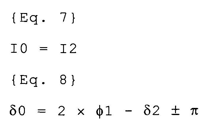
Even if the above equations are rewritten as the equations below, they are mathematically equivalent. In the block diagram inFIG. 5 , the equations below are used.
Asine wave generator 502 generates the circulating current command value feedforward term I0FF* as a sine wave signal having root-mean-square value 10 and phase angle δ0. - Instead of an algorithm that is completely the same as in the block diagram shown in
FIG. 4 , thefeedforward calculator 310 can also use another algorithm if signals that are mathematically equivalent to the equations in [Eq. 7] to [Eq. 10] can be output. - The internal structure of the
cluster balancing controller 311 will be described with reference toFIG. 6 . - The
cluster balancing controller 311 calculates ΔVCuv, ΔVCvw, and ΔVCwu, which are respectively differences between the given total average DC voltage VC and cluster average DC voltages VCuv, VCvw and VCwu. Thecluster balancing controller 311 then performs αβ conversion on the obtained ΔVCuv, ΔVCvw, and ΔVCwu by using an αβ converting block 601 and obtains [ΔVCα, ΔVCβ] as a vector on an αβ axis. Thecluster balancing controller 311 further calculates the sizes ΔVC and amplitude ξ of vectors [ΔVCα, ΔVCβ] through an orthogonal coordinate-polar coordinate convertingblock 602. - The
cluster balancing controller 311 also calculates amplitude φ1 of vectors [Vd, Vq], that is, the phase angle of the line-to-line voltage between phases u and v of the power supply system, from vectors [Vd, Vq] of given positive-phase sequence d-axis voltage Vd and positive-phase sequence q-axis voltage Vq though the orthogonal coordinate-polar coordinate convertingblock 501. - The
sine wave generator 502 outputs the circulating current command value feedback term I0FB* as a sine wave signal that has root-mean-square value I0, which is obtained by multiplying ΔVC by a clusterbalancing control gain 603, and phase angle δ0 (= φ1 - ξ). - Effects obtained by the present invention will be described with reference to
FIG. 7 . -
FIG. 7 shows schematic waveforms of each part in a case in which control in the present invention has been carried out. The waveforms at the top are schematic waveforms of line-to-line voltages VSuv, VSvw, and VSwu of thepower supply system 101, followed by schematic waveforms of currents Iuv, Ivw, and Iwu that flow into the theirrespective reactors 103 andclusters 104 to 106, a schematic waveform of the circular current (I0FF + I0FB), schematic waveforms of DC voltages VCuvj, VCvwj, and VCwuj, and schematic waveforms of DC voltages VCuvfj, VCvwfj, and VCwufj observed after they have passed through theLPFs 301 in that order. The waveforms inFIG. 7 are drawn, assuming that circularcurrent command value 10 ideally follows the command value (I0FF* + I0FB*). - In
FIG. 7 , the horizontal axis indicates time or phase angle, and the vertical axis indicates amplitudes of voltage and current in an arbitrary unit (a.u.). - In the period during which currents Iuv, Ivw, and Iwu include a negative-phase sequence current, circulating current 10 is flowing.
- The mechanism in the present invention will be described below.
- When circulating current 10 controlled by the circulating
current controller 312 is superimposed on currents Iuv*, Ivw*, and Iwu* flowing in theirrespective reactors 103 and theclusters 104 to 106, even if Iuv, Ivw, and Iwu include a negative-phase sequence component, a phase difference between Vuv and Iuv, a phase difference between Vvw and Ivw, and a phase difference between Vwu and Iwu become 90 degrees. That is, active electric power that flows into each cluster and active electric power output from there become zero. Accordingly, active electric power that flowed into each cluster and outputs from there becomes zero, suppressing the DC voltage from being unbalanced. - In the present invention, the zero-phase sequence feedback term I0FB* plays a role of suppressing the DC voltages from being unbalanced due to variations in the characteristics of parts in use and other factors.
- With the
power converter 102 in this embodiment, theclusters 104 to 106 are connected to thepower supply system 101 through theirrespective reactors 103. - The present invention can also be applied to a case in which the
clusters 104 to 106 are each connected to thepower supply system 101 through a transformer instead of thereactor 103. - The present invention can also be applied to a case in which the
clusters 104 to 106 are each connected to thepower supply system 101 through both therector 103 and a transformer. - A second embodiment of the present invention will be described below.
- In the first embodiment, negative-phase sequence current command values Id2* and Iq2* have been given to the
feedforward calculator 310. In the second embodiment, however, actual negative-phase sequence currents Id2 and Iq2 are given instead of Id2* and Iq2*. - Accordingly, even if the
current controller 308 cannot control currents as intended due to some disturbance, that is, even if Id2 is not Id2* or Iq2 is not Iq2*, the effect that active electric power that flows into theclusters 104 to 106 can be made approximately zero is obtained. - Differences between the first embodiment and the second embodiment lie in the control block and feedforward calculator. Accordingly, the control block and feedforward calculator in the second embodiment will be described below with reference to
FIGs. 8 and9 . - In the control block in
FIG. 8 , currents Iuv, Ivw, and Iwu are given to afeedforward calculator 801. - Next, the internal structure of the
feedforward calculator 801 will be described with reference toFIG. 9 . - The
feedforward calculator 801 uses a negative-phase sequencedq converting block 307 to perform negative-phase sequence dq conversion on currents Iuv, Ivw, and Iwu, and calculates a moving average in which a half cycle of the power supply system is handled as a time window through the movingaverage calculator 401, obtaining negative-phase sequence d-axis current <Id2> and negative-phase sequence q-axis current <Iq2>. Thefeedforward calculator 801 also obtains root-mean-square value I2 and phase angle δ2 of the negative-phase sequence current from the sizes and amplitudes of vectors [<Id2>, <Iq2>] through the orthogonal coordinate-polar coordinate convertingblock 501. - The
feedforward calculator 801 also uses the positive-phase sequencedq converting block 306 to perform negative-phase sequence dq conversion on phase voltages VSu, VSv, and VSw of thepower supply system 101, and calculates a moving average in which a half cycle of the power supply system is handled as a time window through the movingaverage calculator 401, obtaining positive-phase sequence d-axis voltage <Vd1> and positive-phase sequence q-axis voltage <Vq1>. Thefeedforward calculator 801 also obtains positive-phase sequence voltage root-mean-square value V1 and negative-phase sequence voltage phase angle φ1 from the sizes and amplitudes of vectors [<Vd2>, <Vq2>] through the orthogonal coordinate-polar coordinate convertingblock 501. - The inventors found from I2, δ2, V1, and φ1 obtained above that active electric power that flows into the
clusters 104 to 106 can be made zero by applying the circulating current command value feedforward term I0FF*, which has root-mean-square value I0 and phase angle δ0 represented by the equations below, to the clusters.
Even if the above equations are rewritten as the equations below, they are mathematically equivalent. In the block diagram inFIG. 5 , the equations below are used.
Thesine wave generator 502 generates the circulating current command value feedforward term I0FF* as a sine wave signal having root-mean-square value 10 and phase angle δ0. - The second embodiment is the same as the first embodiment except the control block (
FIG. 3 ) andfeedforward calculator 801, which have been described above. - A third embodiment of the present invention will be described below.
- In the third embodiment, even if the three phases of the voltage of the
power supply system 101 are unbalanced and include negative-phase sequence components, the effect that active electric power that flows into theclusters 104 to 106 and active electric power output from there can be made zero can be obtained as in the first and second embodiments. - The third embodiment is characterized in that the
feedforward calculator 801, shown inFIG. 9 , in the second embodiment is replaced with a negative-phase sequence voltageready feedforward calculator 1001 shown inFIG. 10 . - The negative-phase sequence voltage
ready feedforward calculator 1001 obtains positive-phase sequence d-axis current <Id1> and positive-phase sequence q-axis current <Iq1> from currents Iuv, Ivw, and Iwu through the positive-phase sequencedq converting block 306 and movingaverage calculator 401. The negative-phase sequence voltageready feedforward calculator 1001 further obtains positive-phase sequence current root-mean-square value I1 and positive-phase sequence current phase angle δ1 from the sizes and amplitudes of vectors [<Id1>, <Iq1>] through the orthogonal coordinate-polar coordinateconverter 501. - The negative-phase sequence voltage
ready feedforward calculator 1001 obtains negative-phase sequence d-axis current <Id2> and negative-phase sequence q-axis current <Iq2> from currents Iu, Iv, and Iw through the negative-phase sequencedq converting block 307 and movingaverage calculator 401. The negative-phase sequence voltageready feedforward calculator 1001 further obtains negative-phase sequence current root-mean-square value I2 and negative-phase sequence current phase angle δ2 from the absolute value and angle of vector [<Id2>, <Iq2>] through the orthogonal coordinate-polar coordinateconverter 501. - The negative-phase sequence voltage
ready feedforward calculator 1001 obtains positive-phase sequence d-axis voltage <Vd1> and positive-phase sequence q-axis voltage <Vq1> from voltages VSuv, VSvw, and VSwu through the positive-phase sequencedq converting block 306 and movingaverage calculator 401. The negative-phase sequence voltageready feedforward calculator 1001 further obtains positive-phase sequence voltage root-mean-square value V1 and positive-phase sequence voltage phase angle φ1 from the absolute value and angle of vector [<Vd1>, <Vq1>] through the orthogonal coordinate-polar coordinateconverter 501. - The negative-phase sequence voltage
ready feedforward calculator 1001 obtains negative-phase sequence d-axis voltage <Vd2> and negative-phase sequence q-axis voltage <Vq2> from voltages VSuv, VSvw, and VSwu through the negative-phase sequencedq converting block 307 and movingaverage calculator 401. The negative-phase sequence voltageready feedforward calculator 1001 further obtains positive-phase sequence voltage root-mean-square value V2 and positive-phase sequence voltage phase angle φ2 from the sizes and amplitudes of vector [<Vd2>, <Vq2>] through the orthogonal coordinate-polar coordinateconverter 501. - The inventors found that even if voltages VSuv, VSvw, and VSwu include negative-phase sequence components, active electric power that flows into the clusters and active electric power output from there can be made zero by giving the circular current command value feedforward term I0FF* having root-mean-
square value 10 and phase angle δ0, represented by the equations below, to the circularcurrent controller 312.
When the zero-phase having root-mean-square value I0 and phase angle δ0, which are represented by the above equations, is superimposed on currents Iuv, Ivw, and Iwu, a phase difference between Vuv and Iuv, a phase difference between Vvw and Ivw, and a phase difference between Vwu and Iwu all become 90 degrees. That is, active electric power that flows into each cluster and active electric power output from there become zero, suppressing the DC voltage from being unbalanced. - Instead of an algorithm that is completely the same as in the block diagram shown in
FIG. 10 , the negative-phase sequence voltageready feedforward calculator 1001 can also use another algorithm if signals that are mathematically equivalent to the equations in [Eq. 14] and [Eq. 15] can be output. - With the
power converter 102 in this embodiment, theclusters 104 to 106 are connected to thepower supply system 101 through theirrespective reactors 103. - The present invention can also be applied to a case in which the
clusters 104 to 106 are each connected to thepower supply system 101 through a transformer instead of thereactor 103. - The present invention can also be applied to a case in which the
clusters 104 to 106 are each connected to thepower supply system 101 through both therector 103 and a transform. - 101 ... power supply system, 102 ... power converter, 103 ... reactor, 104 ... uv-phase cluster, 105 ... vw-phase cluster, 106 ... wu-phase cluster, 107 ... unit cell, 201 ... x-phase upper element, 202 ... x-phase lower element, 203 ... y-phase upper element, 204 ... y-phase lower element, 205 ... DC capacitor, 301 ... low-pass filter (LPF), 302 ... average calculator, 303 ... total average DC voltage controller, 304 ... total average DC voltage control gain, 305 ... compensating current value calculator, 306 ... positive-phase sequence dq converting block, 307 ... negative-phase sequence dq converting block, 308 ... current controller, 309 ... voltage command value divider, 310 ... feedforward calculator, 311 ... cluster balancing controller, 312 ... circular current controller, 313 ... circular current control gain, 401 ... moving average calculator, 501 ... orthogonal coordinate-polar coordinate converter, 502 ... sine wave generator, 601 ... αβ converting block, 602 ... orthogonal coordinate-polar coordinate converting block, 603 ... cluster balancing control gain, 801 ... feedforward calculator that uses actual currents, 1001 ... negative-phase sequence voltage ready feedforward calculator.
Claims (7)
- A power converter that has a delta-connected cascade multi-level converter (CMC) linked to a power supply system, the CMC being formed by delta-connecting series circuits, each of which is formed with a reactor and a cluster, the cluster being a series circuit formed with one or a plurality of unit cells, comprising a function by which a positive-phase sequence reactive current and a negative-phase sequence current caused by an unbalanced load linked to the power supply system are substantially compensated by a positive-phase sequence reactive current and a negative-phase sequence current that are simultaneously output by the power converter.
- The power converter according to Claim 1, further comprising a function by which a voltage across a DC capacitor in each of the plurality of unit cells is balanced.
- The power converter according to Claim 1 or 2, further comprising a function by which if the phase angle of the positive-phase sequence component included in a voltage of the power supply system is denoted φ1 and the negative-phase sequence current command value of the power converter or the root-mean-square value of an actual negative-phase sequence current and the phase angle of the current are respectively denoted I2 and δ2, each cluster flows a circular current having root-mean-square value 10 and phase angle δ0, which are represented by equations below.

- The power converter according to any one of Claims 1 to 3, further comprising a function by which if the root-mean-square value and phase angle of the positive-phase sequence component included in the voltage of the power supply system are respectively denoted V1 and φ1, the root-mean-square value and phase angle of the negative-phase sequence component included in the voltage of the power supply system are respectively denoted V2 and φ2, the command value of the current that flows into the cluster or the root-mean-square value of the positive-phase sequence component of an actual current and the phase angle of the positive-phase sequence component are respectively denoted I1 and δ1, and the root-mean-square value and phase angle of the negative-phase sequence component of the actual current are respectively denoted I2 and δ2, each cluster outputs a circular current having root-mean-square value 10 and phase angle δ0, which are substantially represented by equations below.


- The power converter according to any one of Claims 1 to 4, wherein
moving average calculation in which a half cycle of the frequency of the power supply system or an integer multiple of the half cycle is handled as a time window is used in detection of the voltages and currents as well as the phase angles of the voltages and currents (V1, φ1, V2, φ2, I1, δ1, I2, and δ2). - The power converter according to any one of Claims 1 to 3, wherein the unit cell is a single-phase full bridge.
- The power converter according to any one of Claims 1 to 3, wherein a transformer is connected in series with the reactor.
Applications Claiming Priority (2)
| Application Number | Priority Date | Filing Date | Title |
|---|---|---|---|
| JP2010091896A JP5537235B2 (en) | 2010-04-13 | 2010-04-13 | Power converter |
| PCT/JP2011/058567 WO2011129223A1 (en) | 2010-04-13 | 2011-04-05 | Power converter |
Publications (1)
| Publication Number | Publication Date |
|---|---|
| EP2560065A1 true EP2560065A1 (en) | 2013-02-20 |
Family
ID=44798600
Family Applications (1)
| Application Number | Title | Priority Date | Filing Date |
|---|---|---|---|
| EP11768744A Withdrawn EP2560065A1 (en) | 2010-04-13 | 2011-04-05 | Power converter |
Country Status (4)
| Country | Link |
|---|---|
| EP (1) | EP2560065A1 (en) |
| JP (1) | JP5537235B2 (en) |
| CN (1) | CN102822763B (en) |
| WO (1) | WO2011129223A1 (en) |
Cited By (5)
| Publication number | Priority date | Publication date | Assignee | Title |
|---|---|---|---|---|
| EP2983284A4 (en) * | 2013-04-02 | 2016-11-30 | Mitsubishi Electric Corp | Power conversion device |
| US9590483B1 (en) | 2015-10-15 | 2017-03-07 | Ge Energy Power Conversion Technology Ltd | Control of balance of arm capacitor voltages in STATCOMS based on chain links of H bridge modules |
| US9712084B2 (en) | 2014-01-06 | 2017-07-18 | Mitsubishi Electric Corporation | Electric power conversion device |
| US10199954B2 (en) | 2013-10-02 | 2019-02-05 | General Electric Technology Gmbh | Voltage source converter |
| EP3627684B1 (en) * | 2017-05-17 | 2022-02-09 | Mitsubishi Electric Corporation | Power conversion device |
Families Citing this family (23)
| Publication number | Priority date | Publication date | Assignee | Title |
|---|---|---|---|---|
| JPS6096104A (en) * | 1983-10-27 | 1985-05-29 | Toshiba Corp | Controlling method of electric railcar |
| JP5800154B2 (en) * | 2011-01-18 | 2015-10-28 | 国立大学法人東京工業大学 | Power converter and control method thereof |
| CN102522906B (en) * | 2011-12-22 | 2014-01-08 | 东南大学 | Voltage balance and power balance control method of cascaded H bridge converter |
| KR101221159B1 (en) * | 2011-12-30 | 2013-01-10 | 연세대학교 산학협력단 | Multilevel converter controlling method |
| WO2014030202A1 (en) * | 2012-08-20 | 2014-02-27 | 東芝三菱電機産業システム株式会社 | Power converter |
| JP5993675B2 (en) * | 2012-09-14 | 2016-09-14 | 株式会社日立製作所 | Power converter, power conversion system, and control method for power converter |
| JP5992317B2 (en) * | 2012-12-20 | 2016-09-14 | 株式会社東芝 | Power converter |
| CN103036238B (en) * | 2012-12-24 | 2015-02-04 | 珠海万力达电气自动化有限公司 | Control structure and method of chain-type active power filter (FAPF) linkage unit bypass |
| CN103088220A (en) * | 2013-01-30 | 2013-05-08 | 东南大学 | Three-phase-equilibrium electroslag refining furnace |
| JP6196071B2 (en) * | 2013-05-28 | 2017-09-13 | 株式会社東芝 | Power converter |
| JP2014233126A (en) * | 2013-05-28 | 2014-12-11 | 株式会社東芝 | Power converter |
| CN103475250B (en) * | 2013-09-25 | 2016-10-19 | 湖南大学 | Consider the general loop current control method for modular multi-level converter of low-frequency oscillation |
| CN103501013A (en) * | 2013-10-21 | 2014-01-08 | 安徽天沃电气技术有限公司 | Three-phase unbalanced load power factor correction and system current balance equipment |
| JP6289887B2 (en) * | 2013-12-04 | 2018-03-07 | 株式会社東芝 | Power converter |
| JP6326235B2 (en) * | 2014-01-30 | 2018-05-16 | 株式会社日立製作所 | Power conversion conversion and power conversion method |
| JP2016067124A (en) * | 2014-09-25 | 2016-04-28 | 株式会社日立製作所 | Power compensator and power compensation method |
| JP6370702B2 (en) * | 2014-12-24 | 2018-08-08 | 株式会社東芝 | Power converter |
| US10218285B2 (en) | 2015-10-19 | 2019-02-26 | Siemens Aktiengesellschaft | Medium voltage hybrid multilevel converter and method for controlling a medium voltage hybrid multilevel converter |
| JP6686562B2 (en) * | 2016-03-11 | 2020-04-22 | 富士電機株式会社 | Power converter controller |
| JP6876585B2 (en) * | 2017-09-22 | 2021-05-26 | 株式会社日立製作所 | Power converter and power conversion system |
| JP7040077B2 (en) * | 2018-02-07 | 2022-03-23 | 富士電機株式会社 | Power converter |
| CN109521276A (en) * | 2018-10-19 | 2019-03-26 | 湖南大学 | A kind of high-voltage large-capacity impedance measurement device and its disturbance control method |
| JP7363033B2 (en) * | 2019-01-11 | 2023-10-18 | 富士電機株式会社 | power converter |
Family Cites Families (5)
| Publication number | Priority date | Publication date | Assignee | Title |
|---|---|---|---|---|
| CN1305198C (en) * | 2003-06-18 | 2007-03-14 | 清华大学 | Direct current voltage balancing circuit of reactive generating device based on chained invertor |
| JP5002812B2 (en) * | 2006-03-14 | 2012-08-15 | 国立大学法人東京工業大学 | Self-excited reactive power compensator, capacitor voltage control method in self-excited reactive power compensator, power storage device, and power storage device control method |
| JP4523950B2 (en) * | 2007-02-15 | 2010-08-11 | 株式会社日立製作所 | Reactive power compensation device, reactive power compensation system, and reactive power compensation method |
| JP5261967B2 (en) * | 2007-04-17 | 2013-08-14 | 富士電機株式会社 | Voltage fluctuation compensator control method |
| CN101051751A (en) * | 2007-05-14 | 2007-10-10 | 上海艾帕电力电子有限公司 | Active power filter including power unit and its control method |
-
2010
- 2010-04-13 JP JP2010091896A patent/JP5537235B2/en active Active
-
2011
- 2011-04-05 CN CN201180018422.6A patent/CN102822763B/en not_active Expired - Fee Related
- 2011-04-05 WO PCT/JP2011/058567 patent/WO2011129223A1/en active Application Filing
- 2011-04-05 EP EP11768744A patent/EP2560065A1/en not_active Withdrawn
Non-Patent Citations (1)
| Title |
|---|
| See references of WO2011129223A1 * |
Cited By (5)
| Publication number | Priority date | Publication date | Assignee | Title |
|---|---|---|---|---|
| EP2983284A4 (en) * | 2013-04-02 | 2016-11-30 | Mitsubishi Electric Corp | Power conversion device |
| US10199954B2 (en) | 2013-10-02 | 2019-02-05 | General Electric Technology Gmbh | Voltage source converter |
| US9712084B2 (en) | 2014-01-06 | 2017-07-18 | Mitsubishi Electric Corporation | Electric power conversion device |
| US9590483B1 (en) | 2015-10-15 | 2017-03-07 | Ge Energy Power Conversion Technology Ltd | Control of balance of arm capacitor voltages in STATCOMS based on chain links of H bridge modules |
| EP3627684B1 (en) * | 2017-05-17 | 2022-02-09 | Mitsubishi Electric Corporation | Power conversion device |
Also Published As
| Publication number | Publication date |
|---|---|
| JP5537235B2 (en) | 2014-07-02 |
| CN102822763A (en) | 2012-12-12 |
| WO2011129223A1 (en) | 2011-10-20 |
| JP2011223784A (en) | 2011-11-04 |
| CN102822763B (en) | 2014-10-22 |
Similar Documents
| Publication | Publication Date | Title |
|---|---|---|
| EP2560065A1 (en) | Power converter | |
| EP2560275A1 (en) | Power converter | |
| Akagi et al. | Control and performance of a transformerless cascade PWM STATCOM with star configuration | |
| Lee et al. | Novel discontinuous PWM method of a three-level inverter for neutral-point voltage ripple reduction | |
| JP5993675B2 (en) | Power converter, power conversion system, and control method for power converter | |
| Acuna et al. | Improved active power filter performance for renewable power generation systems | |
| Varschavsky et al. | Cascaded nine-level inverter for hybrid-series active power filter, using industrial controller | |
| EP2443717B1 (en) | An arrangement for exchanging power | |
| AU2009344066B2 (en) | An arrangement for exchanging power | |
| EP3093976B1 (en) | Electric power conversion system | |
| CN105324903A (en) | Methods and devices for controlling active power flow in a three-phase modular multilevel converter | |
| Elserougi et al. | A transformerless STATCOM based on a hybrid Boost Modular Multilevel Converter with reduced number of switches | |
| Ghias et al. | Voltage balancing strategy for a five-level flying capacitor converter using phase disposition PWM with sawtooth-shaped carriers | |
| Isik et al. | A feedforward current control strategy for a MMC based point to point HVDC systems | |
| Eremia et al. | VSC–HVDC Transmission | |
| Islam et al. | Power converter topologies for grid-integrated medium-voltage applications | |
| Lauttamus et al. | Comparison of five-level voltage-source inverter based STATCOMs | |
| JP5714705B2 (en) | Power converter and its control device | |
| Chen et al. | A SVPWM based on fluctuate capacitor voltage in 3L-NPC back-to-back converter applied to wind energy | |
| JP7249471B1 (en) | power converter | |
| Raj et al. | Five-level multiple-pole mutlilevel diode-clamped inverter scheme for reactive power compensation | |
| Yoshii et al. | A 6.6‐kV transformerless cascade PWM STATCOM. Experimental verification by a three‐phase 200‐V, 10‐kVa laboratory system | |
| Reddy et al. | Performance comparison of star connected cascaded STATCOM using different PWM techniques | |
| ASLAM et al. | Space Vector Control NPC Three Level Inverter Based STATCOM With Balancing DC Capacitor Voltage | |
| Reddy et al. | Study of Star Connected Cascaded H-Bridge STATCOM using Different PWM Techniques |
Legal Events
| Date | Code | Title | Description |
|---|---|---|---|
| PUAI | Public reference made under article 153(3) epc to a published international application that has entered the european phase |
Free format text: ORIGINAL CODE: 0009012 |
|
| 17P | Request for examination filed |
Effective date: 20121031 |
|
| AK | Designated contracting states |
Kind code of ref document: A1 Designated state(s): AL AT BE BG CH CY CZ DE DK EE ES FI FR GB GR HR HU IE IS IT LI LT LU LV MC MK MT NL NO PL PT RO RS SE SI SK SM TR |
|
| DAX | Request for extension of the european patent (deleted) | ||
| STAA | Information on the status of an ep patent application or granted ep patent |
Free format text: STATUS: THE APPLICATION HAS BEEN WITHDRAWN |
|
| 18W | Application withdrawn |
Effective date: 20171006 |