EP2560044A1 - Method for manufacturing electronic substrate, method for manufacturing liquid crystal display device, electronic substrate, and liquid crystal display device - Google Patents
Method for manufacturing electronic substrate, method for manufacturing liquid crystal display device, electronic substrate, and liquid crystal display device Download PDFInfo
- Publication number
- EP2560044A1 EP2560044A1 EP11768650A EP11768650A EP2560044A1 EP 2560044 A1 EP2560044 A1 EP 2560044A1 EP 11768650 A EP11768650 A EP 11768650A EP 11768650 A EP11768650 A EP 11768650A EP 2560044 A1 EP2560044 A1 EP 2560044A1
- Authority
- EP
- European Patent Office
- Prior art keywords
- conductive layer
- layer
- conductive
- insulating layer
- liquid crystal
- Prior art date
- Legal status (The legal status is an assumption and is not a legal conclusion. Google has not performed a legal analysis and makes no representation as to the accuracy of the status listed.)
- Withdrawn
Links
- 239000000758 substrate Substances 0.000 title claims abstract description 97
- 238000004519 manufacturing process Methods 0.000 title claims abstract description 40
- 238000000034 method Methods 0.000 title claims abstract description 34
- 239000004973 liquid crystal related substance Substances 0.000 title claims description 49
- 238000005530 etching Methods 0.000 claims abstract description 16
- 239000010410 layer Substances 0.000 description 278
- 239000010408 film Substances 0.000 description 90
- 239000000463 material Substances 0.000 description 38
- 239000004065 semiconductor Substances 0.000 description 27
- VYPSYNLAJGMNEJ-UHFFFAOYSA-N Silicium dioxide Chemical compound O=[Si]=O VYPSYNLAJGMNEJ-UHFFFAOYSA-N 0.000 description 14
- 239000011229 interlayer Substances 0.000 description 14
- 239000011521 glass Substances 0.000 description 9
- 238000000206 photolithography Methods 0.000 description 9
- 239000012535 impurity Substances 0.000 description 8
- XUIMIQQOPSSXEZ-UHFFFAOYSA-N Silicon Chemical compound [Si] XUIMIQQOPSSXEZ-UHFFFAOYSA-N 0.000 description 7
- 239000003990 capacitor Substances 0.000 description 7
- 229910052681 coesite Inorganic materials 0.000 description 7
- 239000004020 conductor Substances 0.000 description 7
- 229910052906 cristobalite Inorganic materials 0.000 description 7
- 238000005468 ion implantation Methods 0.000 description 7
- 229910052751 metal Inorganic materials 0.000 description 7
- 239000002184 metal Substances 0.000 description 7
- 229910052710 silicon Inorganic materials 0.000 description 7
- 239000010703 silicon Substances 0.000 description 7
- 239000000377 silicon dioxide Substances 0.000 description 7
- 229910052682 stishovite Inorganic materials 0.000 description 7
- 229910052905 tridymite Inorganic materials 0.000 description 7
- 229910052782 aluminium Inorganic materials 0.000 description 6
- XAGFODPZIPBFFR-UHFFFAOYSA-N aluminium Chemical compound [Al] XAGFODPZIPBFFR-UHFFFAOYSA-N 0.000 description 6
- 238000005268 plasma chemical vapour deposition Methods 0.000 description 6
- 230000015572 biosynthetic process Effects 0.000 description 5
- 230000007797 corrosion Effects 0.000 description 5
- 238000005260 corrosion Methods 0.000 description 5
- 238000002425 crystallisation Methods 0.000 description 5
- 230000008025 crystallization Effects 0.000 description 5
- 239000011159 matrix material Substances 0.000 description 5
- 229910044991 metal oxide Inorganic materials 0.000 description 5
- 150000004706 metal oxides Chemical class 0.000 description 5
- 150000002739 metals Chemical class 0.000 description 5
- 238000004544 sputter deposition Methods 0.000 description 5
- IJGRMHOSHXDMSA-UHFFFAOYSA-N Atomic nitrogen Chemical compound N#N IJGRMHOSHXDMSA-UHFFFAOYSA-N 0.000 description 4
- 239000011810 insulating material Substances 0.000 description 4
- 238000002294 plasma sputter deposition Methods 0.000 description 4
- 239000011347 resin Substances 0.000 description 4
- 229920005989 resin Polymers 0.000 description 4
- 238000003860 storage Methods 0.000 description 4
- 239000010409 thin film Substances 0.000 description 4
- 239000010936 titanium Substances 0.000 description 4
- UFHFLCQGNIYNRP-UHFFFAOYSA-N Hydrogen Chemical compound [H][H] UFHFLCQGNIYNRP-UHFFFAOYSA-N 0.000 description 3
- MUBZPKHOEPUJKR-UHFFFAOYSA-N Oxalic acid Chemical compound OC(=O)C(O)=O MUBZPKHOEPUJKR-UHFFFAOYSA-N 0.000 description 3
- 229910052581 Si3N4 Inorganic materials 0.000 description 3
- 229910045601 alloy Inorganic materials 0.000 description 3
- 239000000956 alloy Substances 0.000 description 3
- 150000001875 compounds Chemical class 0.000 description 3
- 230000000694 effects Effects 0.000 description 3
- 239000001257 hydrogen Substances 0.000 description 3
- 229910052739 hydrogen Inorganic materials 0.000 description 3
- 238000000059 patterning Methods 0.000 description 3
- HQVNEWCFYHHQES-UHFFFAOYSA-N silicon nitride Chemical compound N12[Si]34N5[Si]62N3[Si]51N64 HQVNEWCFYHHQES-UHFFFAOYSA-N 0.000 description 3
- -1 tantalum (Ta) Chemical class 0.000 description 3
- PXHVJJICTQNCMI-UHFFFAOYSA-N Nickel Chemical compound [Ni] PXHVJJICTQNCMI-UHFFFAOYSA-N 0.000 description 2
- 229910000577 Silicon-germanium Inorganic materials 0.000 description 2
- RTAQQCXQSZGOHL-UHFFFAOYSA-N Titanium Chemical compound [Ti] RTAQQCXQSZGOHL-UHFFFAOYSA-N 0.000 description 2
- 230000004913 activation Effects 0.000 description 2
- UMIVXZPTRXBADB-UHFFFAOYSA-N benzocyclobutene Chemical compound C1=CC=C2CCC2=C1 UMIVXZPTRXBADB-UHFFFAOYSA-N 0.000 description 2
- 239000010949 copper Substances 0.000 description 2
- 230000007547 defect Effects 0.000 description 2
- 238000002149 energy-dispersive X-ray emission spectroscopy Methods 0.000 description 2
- 230000005669 field effect Effects 0.000 description 2
- 238000005984 hydrogenation reaction Methods 0.000 description 2
- 229910010272 inorganic material Inorganic materials 0.000 description 2
- 239000011147 inorganic material Substances 0.000 description 2
- 229910052757 nitrogen Inorganic materials 0.000 description 2
- 239000011368 organic material Substances 0.000 description 2
- 239000004033 plastic Substances 0.000 description 2
- 229910052719 titanium Inorganic materials 0.000 description 2
- 230000003313 weakening effect Effects 0.000 description 2
- 239000004925 Acrylic resin Substances 0.000 description 1
- 229920000178 Acrylic resin Polymers 0.000 description 1
- ZOXJGFHDIHLPTG-UHFFFAOYSA-N Boron Chemical compound [B] ZOXJGFHDIHLPTG-UHFFFAOYSA-N 0.000 description 1
- RYGMFSIKBFXOCR-UHFFFAOYSA-N Copper Chemical compound [Cu] RYGMFSIKBFXOCR-UHFFFAOYSA-N 0.000 description 1
- ZOKXTWBITQBERF-UHFFFAOYSA-N Molybdenum Chemical compound [Mo] ZOKXTWBITQBERF-UHFFFAOYSA-N 0.000 description 1
- 239000004952 Polyamide Substances 0.000 description 1
- 239000004642 Polyimide Substances 0.000 description 1
- BQCADISMDOOEFD-UHFFFAOYSA-N Silver Chemical compound [Ag] BQCADISMDOOEFD-UHFFFAOYSA-N 0.000 description 1
- LEVVHYCKPQWKOP-UHFFFAOYSA-N [Si].[Ge] Chemical compound [Si].[Ge] LEVVHYCKPQWKOP-UHFFFAOYSA-N 0.000 description 1
- 229910052783 alkali metal Inorganic materials 0.000 description 1
- 229910021417 amorphous silicon Inorganic materials 0.000 description 1
- 230000004888 barrier function Effects 0.000 description 1
- 229910052796 boron Inorganic materials 0.000 description 1
- 239000003054 catalyst Substances 0.000 description 1
- 239000000470 constituent Substances 0.000 description 1
- 229910052802 copper Inorganic materials 0.000 description 1
- 238000009792 diffusion process Methods 0.000 description 1
- 230000005684 electric field Effects 0.000 description 1
- 238000010304 firing Methods 0.000 description 1
- 238000010438 heat treatment Methods 0.000 description 1
- 230000006872 improvement Effects 0.000 description 1
- AMGQUBHHOARCQH-UHFFFAOYSA-N indium;oxotin Chemical compound [In].[Sn]=O AMGQUBHHOARCQH-UHFFFAOYSA-N 0.000 description 1
- FBAFATDZDUQKNH-UHFFFAOYSA-M iron chloride Chemical compound [Cl-].[Fe] FBAFATDZDUQKNH-UHFFFAOYSA-M 0.000 description 1
- 238000005499 laser crystallization Methods 0.000 description 1
- 238000004518 low pressure chemical vapour deposition Methods 0.000 description 1
- 229910052750 molybdenum Inorganic materials 0.000 description 1
- 239000011733 molybdenum Substances 0.000 description 1
- 229910052759 nickel Inorganic materials 0.000 description 1
- 150000004767 nitrides Chemical class 0.000 description 1
- 235000006408 oxalic acid Nutrition 0.000 description 1
- 230000010287 polarization Effects 0.000 description 1
- 229920002647 polyamide Polymers 0.000 description 1
- 229910021420 polycrystalline silicon Inorganic materials 0.000 description 1
- 229920001690 polydopamine Polymers 0.000 description 1
- 229920001721 polyimide Polymers 0.000 description 1
- 229920005591 polysilicon Polymers 0.000 description 1
- 230000008569 process Effects 0.000 description 1
- 230000009467 reduction Effects 0.000 description 1
- 229910052709 silver Inorganic materials 0.000 description 1
- 239000004332 silver Substances 0.000 description 1
- 239000002356 single layer Substances 0.000 description 1
- 238000004528 spin coating Methods 0.000 description 1
- 239000010935 stainless steel Substances 0.000 description 1
- 229910001220 stainless steel Inorganic materials 0.000 description 1
- 229910052715 tantalum Inorganic materials 0.000 description 1
- GUVRBAGPIYLISA-UHFFFAOYSA-N tantalum atom Chemical compound [Ta] GUVRBAGPIYLISA-UHFFFAOYSA-N 0.000 description 1
- WFKWXMTUELFFGS-UHFFFAOYSA-N tungsten Chemical compound [W] WFKWXMTUELFFGS-UHFFFAOYSA-N 0.000 description 1
- 229910052721 tungsten Inorganic materials 0.000 description 1
- 239000010937 tungsten Substances 0.000 description 1
- YVTHLONGBIQYBO-UHFFFAOYSA-N zinc indium(3+) oxygen(2-) Chemical compound [O--].[Zn++].[In+3] YVTHLONGBIQYBO-UHFFFAOYSA-N 0.000 description 1
Images


Classifications
-
- G—PHYSICS
- G02—OPTICS
- G02F—OPTICAL DEVICES OR ARRANGEMENTS FOR THE CONTROL OF LIGHT BY MODIFICATION OF THE OPTICAL PROPERTIES OF THE MEDIA OF THE ELEMENTS INVOLVED THEREIN; NON-LINEAR OPTICS; FREQUENCY-CHANGING OF LIGHT; OPTICAL LOGIC ELEMENTS; OPTICAL ANALOGUE/DIGITAL CONVERTERS
- G02F1/00—Devices or arrangements for the control of the intensity, colour, phase, polarisation or direction of light arriving from an independent light source, e.g. switching, gating or modulating; Non-linear optics
- G02F1/01—Devices or arrangements for the control of the intensity, colour, phase, polarisation or direction of light arriving from an independent light source, e.g. switching, gating or modulating; Non-linear optics for the control of the intensity, phase, polarisation or colour
- G02F1/13—Devices or arrangements for the control of the intensity, colour, phase, polarisation or direction of light arriving from an independent light source, e.g. switching, gating or modulating; Non-linear optics for the control of the intensity, phase, polarisation or colour based on liquid crystals, e.g. single liquid crystal display cells
- G02F1/133—Constructional arrangements; Operation of liquid crystal cells; Circuit arrangements
- G02F1/136—Liquid crystal cells structurally associated with a semi-conducting layer or substrate, e.g. cells forming part of an integrated circuit
- G02F1/1362—Active matrix addressed cells
- G02F1/136227—Through-hole connection of the pixel electrode to the active element through an insulation layer
-
- G—PHYSICS
- G02—OPTICS
- G02F—OPTICAL DEVICES OR ARRANGEMENTS FOR THE CONTROL OF LIGHT BY MODIFICATION OF THE OPTICAL PROPERTIES OF THE MEDIA OF THE ELEMENTS INVOLVED THEREIN; NON-LINEAR OPTICS; FREQUENCY-CHANGING OF LIGHT; OPTICAL LOGIC ELEMENTS; OPTICAL ANALOGUE/DIGITAL CONVERTERS
- G02F1/00—Devices or arrangements for the control of the intensity, colour, phase, polarisation or direction of light arriving from an independent light source, e.g. switching, gating or modulating; Non-linear optics
- G02F1/01—Devices or arrangements for the control of the intensity, colour, phase, polarisation or direction of light arriving from an independent light source, e.g. switching, gating or modulating; Non-linear optics for the control of the intensity, phase, polarisation or colour
- G02F1/13—Devices or arrangements for the control of the intensity, colour, phase, polarisation or direction of light arriving from an independent light source, e.g. switching, gating or modulating; Non-linear optics for the control of the intensity, phase, polarisation or colour based on liquid crystals, e.g. single liquid crystal display cells
- G02F1/133—Constructional arrangements; Operation of liquid crystal cells; Circuit arrangements
- G02F1/136—Liquid crystal cells structurally associated with a semi-conducting layer or substrate, e.g. cells forming part of an integrated circuit
- G02F1/1362—Active matrix addressed cells
- G02F1/136213—Storage capacitors associated with the pixel electrode
-
- G—PHYSICS
- G02—OPTICS
- G02F—OPTICAL DEVICES OR ARRANGEMENTS FOR THE CONTROL OF LIGHT BY MODIFICATION OF THE OPTICAL PROPERTIES OF THE MEDIA OF THE ELEMENTS INVOLVED THEREIN; NON-LINEAR OPTICS; FREQUENCY-CHANGING OF LIGHT; OPTICAL LOGIC ELEMENTS; OPTICAL ANALOGUE/DIGITAL CONVERTERS
- G02F1/00—Devices or arrangements for the control of the intensity, colour, phase, polarisation or direction of light arriving from an independent light source, e.g. switching, gating or modulating; Non-linear optics
- G02F1/01—Devices or arrangements for the control of the intensity, colour, phase, polarisation or direction of light arriving from an independent light source, e.g. switching, gating or modulating; Non-linear optics for the control of the intensity, phase, polarisation or colour
- G02F1/13—Devices or arrangements for the control of the intensity, colour, phase, polarisation or direction of light arriving from an independent light source, e.g. switching, gating or modulating; Non-linear optics for the control of the intensity, phase, polarisation or colour based on liquid crystals, e.g. single liquid crystal display cells
- G02F1/133—Constructional arrangements; Operation of liquid crystal cells; Circuit arrangements
- G02F1/136—Liquid crystal cells structurally associated with a semi-conducting layer or substrate, e.g. cells forming part of an integrated circuit
- G02F1/1362—Active matrix addressed cells
- G02F1/136286—Wiring, e.g. gate line, drain line
- G02F1/136295—Materials; Compositions; Manufacture processes
-
- G—PHYSICS
- G02—OPTICS
- G02F—OPTICAL DEVICES OR ARRANGEMENTS FOR THE CONTROL OF LIGHT BY MODIFICATION OF THE OPTICAL PROPERTIES OF THE MEDIA OF THE ELEMENTS INVOLVED THEREIN; NON-LINEAR OPTICS; FREQUENCY-CHANGING OF LIGHT; OPTICAL LOGIC ELEMENTS; OPTICAL ANALOGUE/DIGITAL CONVERTERS
- G02F2201/00—Constructional arrangements not provided for in groups G02F1/00 - G02F7/00
- G02F2201/40—Arrangements for improving the aperture ratio
-
- Y—GENERAL TAGGING OF NEW TECHNOLOGICAL DEVELOPMENTS; GENERAL TAGGING OF CROSS-SECTIONAL TECHNOLOGIES SPANNING OVER SEVERAL SECTIONS OF THE IPC; TECHNICAL SUBJECTS COVERED BY FORMER USPC CROSS-REFERENCE ART COLLECTIONS [XRACs] AND DIGESTS
- Y10—TECHNICAL SUBJECTS COVERED BY FORMER USPC
- Y10T—TECHNICAL SUBJECTS COVERED BY FORMER US CLASSIFICATION
- Y10T428/00—Stock material or miscellaneous articles
- Y10T428/24—Structurally defined web or sheet [e.g., overall dimension, etc.]
- Y10T428/24273—Structurally defined web or sheet [e.g., overall dimension, etc.] including aperture
- Y10T428/24322—Composite web or sheet
- Y10T428/24331—Composite web or sheet including nonapertured component
Definitions
- the present invention relates to a method for manufacturing an electronic substrate, a method for manufacturing a liquid crystal display device, an electronic substrate, and a liquid crystal display device.
- the present invention specifically relates to a method for manufacturing an electronic substrate that is suitably used for a liquid crystal display device and a method for manufacturing a liquid crystal display device, and an electronic substrate that is suitably used for a liquid crystal display device and a liquid crystal display device.
- Liquid crystal display devices are small, thin, less power-consuming, and light-weight devices, and thus they are used in various electronic devices.
- active-matrix liquid crystal display devices in which each pixel has a switching element, are used in a wide variety of devices such as OA devices (e.g. personal computers), AV devices (e.g. televisions), and portable devices (e.g. mobile phones).
- An active-matrix liquid crystal display device includes a pair of transparent substrates and a liquid crystal layer sandwiched therebetween. On one of the transparent substrates are disposed multiple gate lines and multiple data lines horizontally and vertically, and pixel electrodes are provided on the respective regions partitioned by these lines.
- Each TFT has a gate terminal, a source terminal, and a drain terminal, and the gate terminal, the drain terminal, and the source terminal are connected to a gate line, a data line, and a pixel electrode, respectively.
- an ON signal for switching and an image data signal are supplied to the gate lines and the source lines, respectively, the source terminal and the drain terminal are electrically connected and the image data signal is supplied to the pixel electrode (for example, see Patent Literature 1).
- the present inventors have considered a recent strong demand for improvement of the pixel aperture ratio of liquid crystal display devices, and have focused on, as a method for improving the pixel aperture ratio, a method of forming a CS electrode layer (storage capacitor electrode) for maintaining a pixel electrode capacitance from a translucent material.
- the present inventors have found that, in a process of applying a transparent conductive film such as ITO (indium tin oxide) or IZO (indium zinc oxide) to the entire surface and then performing etching with a hydrochloric or oxalic etchant to form a CS electrode layer, components such as electrodes of the TFT disposed on the layer under the transparent conductive film may be damaged by the etching in some cases. Corrosion of the electrodes of the TFT makes it impossible to electrically connect the pixel electrode and the TFT, resulting in pixel defects.
- a transparent conductive film such as ITO (indium tin oxide) or IZO (indium zinc oxide)
- the present invention is devised in view of the above problems, and it aims to provide a method for producing an electronic substrate that is provided with highly reliable electronic elements and lines.
- the present inventors have performed various studies on a method of patterning lines, electrodes, and the like of an electronic substrate without damages on the electronic elements, such as a TFT, and the lines, and thereby focused on resist arrangement. Then, they have found that, even in the case that a transparent conductive film is formed on a conductive film that serves as an electrode or a line, a resist is conventionally applied only to the transparent conductive film that is used as a line or an electrode, and thereby the line or electrode formed under the transparent conductive film that is to be removed by etching is corroded.
- the present invention relates to a method for manufacturing an electronic substrate which comprises a main substrate, a first conductive layer, a first insulating layer, a second conductive layer, a second insulating layer, and a third conductive layer, laminated in the order set forth, and in which the first conductive layer, the second conductive layer, and the third conductive layer are connected together at an opening that penetrates the first insulating layer and the second insulating layer, the method comprising the steps of: forming the first conductive layer; forming the first insulating layer with an opening which exposes at least a part of the first conductive layer; applying a conductive film to an exposed portion of the first conductive layer and the first insulating layer; forming the second conductive layer that covers a surface of the exposed portion of the first conductive layer by applying a resist to a part of the conductive film and etching the conductive film that does not overlap the resist; forming the second insulating layer with an opening which exposes at least a part of the second insulating layer
- the electronic substrate produced by the manufacturing method of the present invention comprises a main substrate, a first conductive layer, a first insulating layer, a second conductive layer, a second insulating layer, and a third conductive layer, laminated in the order set forth.
- the first conductive layer, the second conductive layer, and the third conductive layer are connected together at an opening that penetrates the first insulating layer and the second insulating layer.
- the main substrate is a substrate on which lines and electronic elements such as transistors, resistors, capacitors, and diodes may be placed.
- the material thereof is not particularly limited, and may be glass, plastic, or the like.
- the first conductive layer, the second conductive layer, and the third conductive layer are connected; this may be expressed as "electrically integrated".
- the first conductive layer, the second conductive layer, and the third conductive layer each may have translucency or may have a light-shielding property.
- the manufacturing method comprises the steps of forming a first conductive layer and forming a first insulating layer with an opening which exposes at least a part of the first conductive layer.
- the opening is a hole (contact hole) for connecting the first conductive layer, the second conductive layer, and the third conductive layer.
- the opening may be formed by photolithography, for example.
- the manufacturing method comprises the steps of applying a conductive film to an exposed portion of the first conductive layer and the first insulating layer, and forming a second conductive layer that covers a surface of the exposed portion of the first conductive layer by applying a resist to a part of the conductive film and etching the conductive film that does not overlap the resist.
- the conductive film that does not overlap the resist is shaved by etching so that electrodes or lines are patterned into a predetermined shape.
- the present step enables to efficiently pattern the second conductive layer into a predetermined shape without damages on the first conductive layer. Since the conductive film under the resist is not removed, part of the conductive film remains as a remaining-film layer on the first conductive layer. Such a remaining-film layer herein is also referred to as the second conductive layer.
- the manufacturing method comprises the steps of forming a second insulating layer with an opening which exposes at least a part of the second conductive layer, and forming a third conductive layer on an exposed portion of the second conductive layer and the second insulating layer.
- the first conductive layer and the third conductive layer are connected via the second conductive layer.
- the first conductive layer is not damaged by etching, and thus highly reliable electronic elements and lines can be obtained.
- the method for manufacturing an electronic substrate of the present invention is formed by such essential steps, and may or may not include other steps. Preferable examples of the method for manufacturing an electronic substrate of the present invention are mentioned in detail below.
- the step of forming the second conductive layer is also a step of forming a fourth conductive layer that is electrically separated from the second conductive layer by applying a resist to another part of the conductive film and etching the conductive film that does not overlap the resist.
- a resist to another part of the conductive film and etching the conductive film that does not overlap the resist.
- the second conductive layer is a component for connecting the first conductive layer and the third conductive layer, and thus it is difficult to have a special use.
- the fourth conductive layer can be used as various lines or electrodes.
- the third conductive layer and the fourth conductive layer form a capacitance at the second insulating film.
- the fourth conductive layer may be disposed between the first insulating layer and the second insulating layer to form a capacitance together with the third conductive layer, if necessary, and it may be used as a capacitor, for example.
- the present invention also relates to a method for manufacturing a liquid crystal display device, the method comprising: manufacturing a liquid crystal display device that comprises a pair of substrates and a liquid crystal layer sandwiched between the substrates, one of the substrates being manufactured by the above manufacturing method, the first insulating layer being an organic insulating layer, the second insulating layer being an inorganic insulating layer, and the second conductive layer and the third conductive layer each having translucency.
- the fourth conductive layer has translucency.
- the first insulating layer is preferably 1 ⁇ m or greater in thickness for the purposes of leveling and of weakening the field effect of the electrodes and lines of the lower layer, and an organic insulating film such as resin is suitable.
- an inorganic insulating film with a low leak current is suitable for the second insulating layer.
- Utility forms of the respective conductive layers include a form that the first conductive layer is used as a drain electrode of a thin-film transistor, the third conductive layer is used as a pixel electrode, and the fourth conductive layer is used as a storage capacitor electrode.
- the method for manufacturing a liquid crystal display device of the present invention is formed by such essential steps, and may or may not include other steps.
- the method for manufacturing a liquid crystal display device of the present invention can produce a liquid crystal display device provided with highly reliable electronic elements and lines while having a high aperture ratio. Since etchants to be used are different in many cases between conductive materials with translucency and conductive materials without translucency, the present invention is particularly suitable in the case of using different conductive materials in combination.
- the material of the first conductive layer and the material of the second conductive layer are preferably different materials, and the material of the first conductive layer and the material of the third conductive layer are preferably different materials.
- the present invention also relates to an electronic substrate, comprising, laminated in the order set forth: a main substrate; a first conductive layer; a first insulating film; a second conductive layer; a second insulating film; and a third conductive layer, the first insulating layer being provided with a first opening which exposes at least a part of the first conductive layer, the second insulating layer being provided with a second opening which exposes at least a part of the second conductive layer, the first conductive layer, the second conductive layer, and the third conductive layer being connected together at the first opening and the second opening, the second conductive layer covering a surface of an exposed portion of the first conductive layer, and the third conductive layer covering a surface of an exposed portion of the second conductive layer.
- the electronic substrate of the present invention is provided with a first opening that penetrates the first insulating layer and a second opening that penetrates the second insulating layer, and these openings serve as holes (contact holes) formed for connecting the first conductive layer, the second conductive layer, and the third conductive layer.
- the second conductive layer covers the surface of the exposed portion of the first conductive layer and the third conductive layer covers the surface of the exposed portion of the second conductive layer. Thus, they are electrically integrated and are in direct contact with each other.
- the electronic substrate of the present invention essentially includes such components, and may or may not include other components. Preferable embodiments of the electronic substrate of the present invention are mentioned in detail below.
- the electronic substrate further comprises a fourth conductive layer which is on the same layer as the second conductive layer and which is electrically separated from the second conductive layer.
- the fourth conductive layer as another conductive component can be formed simultaneously in forming the second conductive layer, and thus the manufacturing step can be simplified.
- the second conductive layer is a component for connecting the first conductive layer and the third conductive layer, and thus it is difficult to have a special use.
- the fourth conductive layer can be used for various lines and electrodes.
- the third conductive layer and the fourth conductive layer form a capacitance at the second insulating film.
- the fourth conductive layer may be sandwiched between the first insulating layer and the second insulating layer to form a capacitance together with the third conductive layer, if necessary, and it may be used as a capacitor, for example.
- the present invention also relates to a liquid crystal display device, comprising: a pair of substrates consisting of the electronic substrate according to claim 6 and an opposite substrate; and a liquid crystal layer sandwiched between the substrates, the first insulating layer being an organic insulating layer, the second insulating layer being an inorganic insulating layer, and the second conductive layer and the third conductive layer each having translucency.
- the fourth conductive layer has translucency.
- the first insulating layer is preferably 1 ⁇ m or greater in thickness for the purposes of leveling and of weakening the field effect of the electrodes and lines of the lower layer, and an organic insulating film such as resin is suitable.
- an inorganic insulating film with a low leak current is suitable for the second insulating layer.
- Utility forms of the respective conductive layers include a form that the first conductive layer is used as a drain electrode of a thin-film transistor, the third conductive layer is used as a pixel electrode, and the fourth conductive layer is used as a storage capacitor electrode.
- the liquid crystal display device of the present invention essentially includes such components, and may or may not include other components.
- the liquid crystal display device of the present invention enables to obtain a liquid crystal display device provided with highly reliable electronic elements and lines while having a high aperture ratio.
- the material of the first conductive layer and the material of the second conductive layer are preferably different materials, and the material of the first conductive layer and the material of the third conductive layer are preferably different materials.
- the method for manufacturing an electronic substrate of the present invention can effectively prevent corrosion of electrodes or lines under a conductive film in the manufacturing steps even though the method includes the step of forming a conductive film on the electrodes or lines of the electronic elements and patterning a part of the conductive film. Thus, a highly reliable electronic substrate can be produced.
- a TFT substrate (electronic substrate) of Embodiment 1 can be used as a substrate of a liquid crystal display device for displays of devices such as mobile phones, PDAs, and game consoles.
- Fig. 1 is a schematic cross-sectional view of a TFT substrate of Embodiment 1.
- the TFT substrate has a base coat layer 12 on a glass substrate (main substrate) 11, and has a TFT on the base coat layer 12.
- the TFT has a semiconductor layer 13, a gate electrode 15, a source electrode 17, and a drain electrode (first conductive layer) 18.
- a gate insulating film 14 is disposed between the semiconductor layer 13 and the gate electrode 15.
- Interlayer films 16 are disposed between the gate electrode 15 and the source electrode 17 and between the gate electrode 15 and the drain electrode 18.
- the semiconductor layer 13 has a channel region 13a overlapping the gate electrode 15, a source region 13b connected to the source electrode 17, a drain region 13c connected to the drain electrode 18, and LDD (lightly doped drain, low impurity concentration) regions 13d between the source region 13b and the channel region and between the drain region 13c and the channel region 13a.
- LDD lightly doped drain, low impurity concentration
- An organic insulating layer (first insulating layer) 19 is formed on the TFT, and a CS electrode layer (fourth electrode layer) 20a is disposed on the organic insulating layer 19.
- An inorganic insulating layer (second insulating layer) 21 is formed on the CS electrode layer 20a, and a pixel electrode (third conductive layer) 22 is disposed on the organic insulating layer 19.
- the CS electrode layer 20a can form a capacitance together with the pixel electrode 22, so that it serves to store an electric potential of the pixel electrode 22 in the liquid crystal display device.
- the pixel electrode 22 is connected to the drain electrode 18 at an opening 24 that penetrates the organic insulating layer 19 and the inorganic insulating layer 21.
- a remaining-film layer (second transparent conductive layer) 20b which is left upon forming the CS electrode layer 20a, is disposed between the drain electrode 18 and the pixel electrode 22 so as to cover the surface of the drain electrode 18.
- the liquid crystal layer at a portion overlapping the TFT does not contribute to image display.
- the region on the right side of a dot line in Fig. 1 serves as a pixel opening D and contributes to image display.
- the respective structures of the TFT substrate of Embodiment 1 will be described in more detail hereinbelow referring to a method for manufacturing the TFT substrate of Embodiment 1.
- the following description supposes the case that the TFT substrate of Embodiment 1 is used as a substrate constituting a liquid crystal display device.
- a glass substrate 11 is prepared.
- the glass substrate 11 may be replaced by another material whose surface has an insulating property (e.g. plastic, silicon, or surface-insulated metal or stainless-steel), and it preferably has translucency.
- another material whose surface has an insulating property (e.g. plastic, silicon, or surface-insulated metal or stainless-steel), and it preferably has translucency.
- the base coat layer 12 with a thickness of 100 to 400 nm is formed.
- the base coat layer 12 may be formed from a silicon-containing insulating material (e.g. SiO 2 , SiN, SiNO) by plasma CVD or sputtering.
- the base coat layer 12 prevents diffusion of impurities such as alkalimetal elements from the glass substrate 11 and reduces variation in the electric properties of the TFTs.
- the base coat layer 12 may have a multilayer structure.
- the semiconductor layer 13 may be formed by forming a non-crystalline semiconductor (amorphous silicon) film by, for example, sputtering, LPCVD, or plasma CVD, then forming a crystalline semiconductor (polysilicon) film by crystallization treatment such as laser crystallization, thermal crystallization, or thermal crystallization using a catalyst such as nickel, and then patterning the film into an island-like shape by photolithography.
- the material of the semiconductor layer 13 is not particularly limited, and is preferably silicon (Si) or a silicon-germanium (SiGe) alloy.
- the gate insulating film 14 may be formed from a silicon-containing insulating material (e.g. SiO 2 , SiN, SiNO) by plasma CVD or sputtering.
- the gate insulating film 14 may have a multilayer structure.
- the material of the gate insulating film 14 is particularly preferably SiO 2 . If the gate insulating film 14 has a multilayer structure, the layer in contact with the semiconductor layer 13 is preferably a SiO 2 layer. Further, the material of the semiconductor layer 13 in this case is preferably silicon (Si). Thereby, the energy level at the interface between the gate insulating film 14 and the semiconductor layer 13 is reduced, so that the electric properties of the TFT can be improved.
- the whole of the semiconductor layer 13 is doped with an impurity element such as boron (B) by ion implantation for the purpose of controlling the threshold voltage of the TFT.
- This ion implantation is performed under the conditions of 50 kV and about 5 ⁇ 10 12 to 3 ⁇ 10 13 cm -2 .
- the concentration of the impurity element in the ion-doped semiconductor layer 13 is about 5 ⁇ 10 16 to 5 ⁇ 10 17 cm -3 .
- a conductive film with a thickness of 200 to 600 nm is formed by sputtering, and then the conductive film is patterned into a predetermined shape by photolithography to form a gate electrode 15.
- a suitable material for the gate electrode 15 include high-melting-point metals such as tantalum (Ta), tungsten (W), titanium (Ti), and molybdenum (Mo), and alloys and compounds mainly containing these high-melting-point metals. Suitable among the compounds mainly containing the high-melting-point metals are nitrides.
- the gate electrode 15 may have a structure in which conductive films formed from these materials are laminated.
- the semiconductor layer 13 is doped with impurities such as nitrogen (N) by ion implantation in a self-alignment manner using the gate electrode 15 as a mask.
- the ion implantation in this case is performed under the conditions of 70 kV and about 1 ⁇ 10 13 to 3 ⁇ 10 13 cm -2 .
- the concentration of the impurity element in the semiconductor layer 13 after the ion implantation is about 1 ⁇ 10 13 to 3 ⁇ 10 13 cm -3 .
- the semiconductor layer 13 under the gate electrode serves as a channel region 13a.
- the semiconductor layer 13 at a region to be an LDD region is masked by a resist
- the semiconductor layer 13 is doped with impurities such as nitrogen (N) by ion implantation.
- the ion implantation in this case is performed under the conditions of 50 kV and about 5 ⁇ 10 15 to 1 ⁇ 10 16 cm -2 .
- the concentration of the impurity element in the ion-doped semiconductor layer 13 is about 1 ⁇ 10 19 to 1 ⁇ 10 20 cm -3 .
- the regions which are ion-doped in this step serve as a source region 13b and a drain region 13c (high-impurity-concentration regions), whereas the regions which are not ion-doped in this step serve as LDD regions 13d in the semiconductor layer 13.
- the interlayer film 16 consists of a first interlayer film 16a and a second interlayer film 16b which are made of different materials and are laminated.
- the first interlayer film 16a and the second interlayer film 16b each may be formed from a silicon-containing insulating material (e.g. SiO 2 , SiN, SiNO) by plasma CVD or sputtering.
- the first interlayer film 16a is formed as a hydrogen-containing silicon nitride (SiN:H) layer with a thickness of 0.2 to 0.4 ⁇ m and the second interlayer film 16b is formed as a SiO 2 layer with a thickness of 0.4 to 0.6 ⁇ m.
- the hydrogen in the silicon nitride layer 16a can be effectively used for hydrogenation and activation of the semiconductor layer 13.
- Examples of the conditions for the hydrogenation and activation include a method of heating at 400°C to 450°C for about 0.5 to 1.0 hour.
- the interlayer film 16 may have a monolayer structure.
- contact holes are formed by photolithography through the interlayer film 16 and the gate insulating film 14 above the source region 13b and the drain region 13c of the semiconductor layer. Thereby, the source region 13b and the drain region 13c of the semiconductor layer are partly exposed.
- a conductive film with a thickness of 400 to 1000 nm is formed by sputtering, and then the conductive film is patterned into a predetermined shape by photolithography to form a source electrode 17 and a drain electrode (first conductive layer) 18.
- the source electrode 17 and the drain electrode 18 are formed on the second interlayer film 16b and in the contact holes. Thereby, the source region 13b of the semiconductor layer is connected to the source electrode 17, and the drain region 13c of the semiconductor layer is connected to the drain electrode 18.
- Suitable materials for the source electrode 17 and the drain electrode 18 are low-resistant metals such as aluminum (Al), copper (Cu), and silver (Ag) and alloys and compounds mainly containing these low-resistant metals. In particular, aluminum (Al) is suitable in order to reduce the wiring resistance.
- the source electrode 17 and the drain electrode 18 may have a structure that the conductive films formed from these materials or other materials are laminated.
- an organic insulating layer (first insulating layer) 19 with a thickness of 1.0 to 3.0 ⁇ m is formed.
- the organic insulating layer 19 may be formed by applying an insulating film material by a method such as spin coating, and then firing the material, if necessary.
- a suitable material of the organic insulating layer 19 include resin materials such as polyimide, acryl, polyamide, polyimideamide, and BCB (benzocyclobutene); in particular, photo-sensitive acrylic resins are suitable.
- a photosensitive resin material enables to form a contact hole only by exposure and development after formation of the organic insulating layer 19.
- the organic insulating layer 19 may have a multilayer structure.
- a contact hole (first opening) is formed by photolithography through the organic insulating layer 19 on the drain electrode 18 such that at least a part of the drain electrode 18 is exposed.
- a transparent conductive film with a thickness of 50 to 300 nm is formed by sputtering, and then a resist is placed on a region to be a CS electrode layer and on the transparent conductive film on the drain electrode 18.
- the transparent conductive film is patterned into a predetermined shape by photolithography, and thereby a CS electrode layer (storage capacitor electrode; fourth conductive layer) 20a and a remaining-film layer (second conductive layer) 20b are formed.
- a suitable material of the transparent conductive film is a translucent metal oxide such as ITO or IZO.
- the ITO may be a non-crystalline (amorphous) one, may be a crystalline (poly) one, or may be one formed by crystallization of an amorphous one.
- a suitable etchant for metal oxides such as ITO and IZO examples include iron chloride etchants and hydrochloric etchants, and oxalic acid.
- etchants In the case that aluminum (Al) is used as the material of the drain electrode, these etchants easily eat into the aluminum.
- Fig. 2 is a schematic view showing the etching step without a resist on ITO on the drain electrode 18. Conventionally, no resist is formed on this portion. Thus, the portion surrounded by the dot line of the drain electrode in Fig. 2 is damaged and the drain electrode 18 and the below-mentioned pixel electrode are not connected to each other.
- a titanium (Ti) layer may be placed as a barrier layer on the upper layer of the aluminum (Al) layer. If this is the case, however, even a slight defect in the formed film causes corrosion to proceed easily.
- Fig. 3 is a schematic view showing the etching step with a resist on ITO on the drain electrode.
- the present invention employs this method.
- the resist 23 used for formation of the CS electrode layer 20a is also placed on the drain electrode, and thus corrosion of the drain electrode 18 can be prevented. As a result, the reliability is improved and the yield is efficiently improved.
- the remaining-film layer 20b on the CS electrode layer 20a and the drain electrode 18 may have a multilayer structure.
- the resistance of a metal oxide such as ITO or IZO is higher than that of a metal such as Al (aluminum).
- the area of the remaining-film layer 20b is small, and thus the layer 20b hardly affects the connection between the drain electrode 18 and the pixel electrode. As a result, the remaining-film layer 20b is formed so as to cover the surface of the exposed portion of the drain electrode 18.
- an inorganic insulating layer (second insulating film) 21 with a thickness of 100 to 400 nm is formed.
- the inorganic insulating layer 21 may be formed by plasma CVD or sputtering using a silicon-containing insulating material (e.g. SiO 2 , SiN, SiNO).
- a silicon-containing insulating material e.g. SiO 2 , SiN, SiNO.
- the inorganic insulating layer 21 is formed as a hydrogen-containing silicon nitride (SiN:H) layer by plasma CVD.
- the inorganic insulating layer 21 may have a multilayer structure.
- a contact hole (second opening) is formed by photolithography through the inorganic insulating layer 21 on the remaining-film layer 20b such that at least a part of the remaining-film layer 20b is exposed.
- a transparent conductive film with a thickness of 30 to 200 nm is formed by sputtering, and the transparent conductive film is patterned into a predetermined shape by photolithography to form a pixel electrode 22.
- the pixel electrode 22 and the drain electrode 18 are connected through the opening 24 that penetrates the organic insulating layer 19 and the interlayer film 16.
- Examples of a suitable material of the pixel electrode 22 include translucent metal oxides such as ITO and IZO.
- the ITO may be a non-crystalline (amorphous) one, may be a crystalline (poly) one, or may be one formed by crystallization of an amorphous one.
- the material of the pixel electrode 22 may be different from that of the CS electrode layer 20a and that of the remaining-film layer 20b.
- examples of the combination of the transparent conductive materials for the CS electrode layer 20a, the remaining-film layer 20b, and the pixel electrode 22 include (1) combination of poly ITO and amorphous ITO, (2) combination of ITO formed by baking and crystalizing an amorphous ITO and amorphous ITO, (3) combination of poly ITO and IZO, (4) combination of ITO formed by baking and crystalizing an amorphous ITO and IZO, and (5) combination of IZO and IZO.
- the shapes of the pixel electrode 22, the CS electrode layer 20a, and the remaining-film layer 20b may be observed using a scanning electron microscope (SEM), for example.
- SEM scanning electron microscope
- the constituents of them may be analyzed by EDX (energy dispersive X-ray spectrometry).
- the aforementioned steps enable to produce a highly reliable TFT substrate which has a low wiring resistance and a high aperture ratio, and in which connection is sufficiently secured.
- Fig. 4 is an enlarged schematic cross-sectional view especially showing a region on the drain electrode of the TFT substrate produced by the manufacturing method of Embodiment 1.
- a resist is formed on the transparent conductive film on the drain electrode 18 in order to protect the drain electrode 18 in the manufacturing method of Embodiment 1.
- a remaining-film layer 20b remains on the drain electrode 18. This is a major characteristic in the case of the manufacturing method of the present invention.
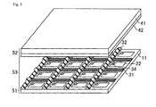
- Fig. 5 is a schematic perspective view of a liquid crystal display device to which the TFT substrate of Embodiment 1 is applied.
- gate electrodes of TFTs (thin-film transistor) 34 are connected to gate lines 31 that extend in the row direction and supply scanning signals, and source electrodes thereof are connected to source lines 32 that extend in the column direction and supply image signals.
- a gate voltage which serves as a scanning signal supplied from a gate driver at a predetermined timing in a pulsed manner, is applied to each gate electrode, an image signal is supplied to the corresponding pixel electrode 22 through the corresponding source electrode, semiconductor layer, and drain electrode at that timing.
- Multiple pixel electrodes 22 are disposed in a matrix manner, and each region overlapping the pixel electrode serves as one pixel.
- the CS electrode layer 20a may be disposed so as to be parallel with the gate line 31 and to cross the pixel electrode 22, for example.
- the liquid crystal display device comprises a pair of substrates consisting of a TFT substrate (electronic substrate) 51 and an opposite substrate 52, and a liquid crystal layer 53 sandwiched between the substrates 51 and 52.
- the opposite substrate 52 has a glass substrate 41 or the like as a main substrate, and has an opposite electrode 42 that forms an electric field in the liquid crystal layer 53 together with the pixel electrode 22 on the glass substrate 41.
- Examples of a suitable material of the opposite electrode 42 include translucent metal oxides such as ITO and IZO.
Landscapes
- Physics & Mathematics (AREA)
- Nonlinear Science (AREA)
- Mathematical Physics (AREA)
- Engineering & Computer Science (AREA)
- Chemical & Material Sciences (AREA)
- Crystallography & Structural Chemistry (AREA)
- Microelectronics & Electronic Packaging (AREA)
- General Physics & Mathematics (AREA)
- Optics & Photonics (AREA)
- Liquid Crystal (AREA)
- Thin Film Transistor (AREA)
- Devices For Indicating Variable Information By Combining Individual Elements (AREA)
- Internal Circuitry In Semiconductor Integrated Circuit Devices (AREA)
- Electrodes Of Semiconductors (AREA)
Abstract
The present invention provides a method for producing an electronic substrate that is provided with highly reliable electronic elements and lines. The method of the present invention provides an electronic substrate which includes a main substrate, a first conductive layer, a first insulating layer, a second conductive layer, a second insulating layer, and a third conductive layer, laminated in the order set forth, and in which the first conductive layer, the second conductive layer, and the third conductive layer are connected together at an opening that penetrates the first insulating layer and the second insulating layer. The manufacturing method includes the steps of: forming the first conductive layer; forming the first insulating layer with an opening which exposes at least a part of the first conductive layer; applying a conductive film to an exposed portion of the first conductive layer and on the first insulating layer; forming the second conductive layer that covers a surface of the exposed portion of the first conductive layer by applying a resist to a part of the conductive film and etching the conductive film that does not overlap the resist; forming the second insulating layer with an opening which exposes at least a part of the second conductive layer; and forming the third conductive layer on an exposed portion of the second conductive layer and on the second insulating layer.
Description
- The present invention relates to a method for manufacturing an electronic substrate, a method for manufacturing a liquid crystal display device, an electronic substrate, and a liquid crystal display device. The present invention specifically relates to a method for manufacturing an electronic substrate that is suitably used for a liquid crystal display device and a method for manufacturing a liquid crystal display device, and an electronic substrate that is suitably used for a liquid crystal display device and a liquid crystal display device.
- Liquid crystal display devices are small, thin, less power-consuming, and light-weight devices, and thus they are used in various electronic devices. In particular, active-matrix liquid crystal display devices, in which each pixel has a switching element, are used in a wide variety of devices such as OA devices (e.g. personal computers), AV devices (e.g. televisions), and portable devices (e.g. mobile phones).
- An active-matrix liquid crystal display device includes a pair of transparent substrates and a liquid crystal layer sandwiched therebetween. On one of the transparent substrates are disposed multiple gate lines and multiple data lines horizontally and vertically, and pixel electrodes are provided on the respective regions partitioned by these lines. Each TFT has a gate terminal, a source terminal, and a drain terminal, and the gate terminal, the drain terminal, and the source terminal are connected to a gate line, a data line, and a pixel electrode, respectively. When an ON signal for switching and an image data signal are supplied to the gate lines and the source lines, respectively, the source terminal and the drain terminal are electrically connected and the image data signal is supplied to the pixel electrode (for example, see Patent Literature 1).
-
- Patent Literature 1:
JP 2007-248892 A - The present inventors have considered a recent strong demand for improvement of the pixel aperture ratio of liquid crystal display devices, and have focused on, as a method for improving the pixel aperture ratio, a method of forming a CS electrode layer (storage capacitor electrode) for maintaining a pixel electrode capacitance from a translucent material.
- As the result of studies, however, the present inventors have found that, in a process of applying a transparent conductive film such as ITO (indium tin oxide) or IZO (indium zinc oxide) to the entire surface and then performing etching with a hydrochloric or oxalic etchant to form a CS electrode layer, components such as electrodes of the TFT disposed on the layer under the transparent conductive film may be damaged by the etching in some cases. Corrosion of the electrodes of the TFT makes it impossible to electrically connect the pixel electrode and the TFT, resulting in pixel defects.
- The present invention is devised in view of the above problems, and it aims to provide a method for producing an electronic substrate that is provided with highly reliable electronic elements and lines.
- The present inventors have performed various studies on a method of patterning lines, electrodes, and the like of an electronic substrate without damages on the electronic elements, such as a TFT, and the lines, and thereby focused on resist arrangement. Then, they have found that, even in the case that a transparent conductive film is formed on a conductive film that serves as an electrode or a line, a resist is conventionally applied only to the transparent conductive film that is used as a line or an electrode, and thereby the line or electrode formed under the transparent conductive film that is to be removed by etching is corroded. They have further found that, with respect to the conductive film on the electrode or line, damages on the conductive film that serves as an electrode or a line can be prevented by leaving the resist on the conductive film purposely so that the conductive film remains. As a result, the present inventors have arrived at the solution to the above problems and completed the present invention.
- In other words, the present invention relates to a method for manufacturing an electronic substrate which comprises a main substrate, a first conductive layer, a first insulating layer, a second conductive layer, a second insulating layer, and a third conductive layer, laminated in the order set forth, and in which the first conductive layer, the second conductive layer, and the third conductive layer are connected together at an opening that penetrates the first insulating layer and the second insulating layer, the method comprising the steps of: forming the first conductive layer; forming the first insulating layer with an opening which exposes at least a part of the first conductive layer; applying a conductive film to an exposed portion of the first conductive layer and the first insulating layer; forming the second conductive layer that covers a surface of the exposed portion of the first conductive layer by applying a resist to a part of the conductive film and etching the conductive film that does not overlap the resist; forming the second insulating layer with an opening which exposes at least a part of the second conductive layer; and forming the third conductive layer on an exposed portion of the second conductive layer and the second insulating layer.
- The electronic substrate produced by the manufacturing method of the present invention comprises a main substrate, a first conductive layer, a first insulating layer, a second conductive layer, a second insulating layer, and a third conductive layer, laminated in the order set forth. In the electronic substrate, the first conductive layer, the second conductive layer, and the third conductive layer are connected together at an opening that penetrates the first insulating layer and the second insulating layer. The main substrate is a substrate on which lines and electronic elements such as transistors, resistors, capacitors, and diodes may be placed. The material thereof is not particularly limited, and may be glass, plastic, or the like. In the electronic substrate, the first conductive layer, the second conductive layer, and the third conductive layer are connected; this may be expressed as "electrically integrated". The first conductive layer, the second conductive layer, and the third conductive layer each may have translucency or may have a light-shielding property.
- The manufacturing method comprises the steps of forming a first conductive layer and forming a first insulating layer with an opening which exposes at least a part of the first conductive layer. The opening is a hole (contact hole) for connecting the first conductive layer, the second conductive layer, and the third conductive layer. The opening may be formed by photolithography, for example.
- The manufacturing method comprises the steps of applying a conductive film to an exposed portion of the first conductive layer and the first insulating layer, and forming a second conductive layer that covers a surface of the exposed portion of the first conductive layer by applying a resist to a part of the conductive film and etching the conductive film that does not overlap the resist. In this step, the conductive film that does not overlap the resist is shaved by etching so that electrodes or lines are patterned into a predetermined shape. Thereby, the first conductive layer under the conductive film that is placed under the resist is not affected by etching. As a result, the present step enables to efficiently pattern the second conductive layer into a predetermined shape without damages on the first conductive layer. Since the conductive film under the resist is not removed, part of the conductive film remains as a remaining-film layer on the first conductive layer. Such a remaining-film layer herein is also referred to as the second conductive layer.
- The manufacturing method comprises the steps of forming a second insulating layer with an opening which exposes at least a part of the second conductive layer, and forming a third conductive layer on an exposed portion of the second conductive layer and the second insulating layer. Thereby, the first conductive layer and the third conductive layer are connected via the second conductive layer. Further, the first conductive layer is not damaged by etching, and thus highly reliable electronic elements and lines can be obtained.
- The method for manufacturing an electronic substrate of the present invention is formed by such essential steps, and may or may not include other steps. Preferable examples of the method for manufacturing an electronic substrate of the present invention are mentioned in detail below.
- Preferably, the step of forming the second conductive layer is also a step of forming a fourth conductive layer that is electrically separated from the second conductive layer by applying a resist to another part of the conductive film and etching the conductive film that does not overlap the resist. Such a method enables to perform the step for protecting the first conductive layer simultaneously with the step for forming other conductive components, so that the manufacturing steps are made more efficient. The second conductive layer is a component for connecting the first conductive layer and the third conductive layer, and thus it is difficult to have a special use. In contrast, the fourth conductive layer can be used as various lines or electrodes.
- Preferably, the third conductive layer and the fourth conductive layer form a capacitance at the second insulating film. The fourth conductive layer may be disposed between the first insulating layer and the second insulating layer to form a capacitance together with the third conductive layer, if necessary, and it may be used as a capacitor, for example.
- The present invention also relates to a method for manufacturing a liquid crystal display device, the method comprising: manufacturing a liquid crystal display device that comprises a pair of substrates and a liquid crystal layer sandwiched between the substrates, one of the substrates being manufactured by the above manufacturing method, the first insulating layer being an organic insulating layer, the second insulating layer being an inorganic insulating layer, and the second conductive layer and the third conductive layer each having translucency. In the case of forming a fourth conductive layer, the fourth conductive layer has translucency. Use of a transparent conductive material as lines and electrodes leads to an improved aperture ratio in comparison with the case that the components are formed from a material having a light-shielding property. Formation of the insulating layers from different materials, that is, from an inorganic material and an organic material, leads to the following effects. The first insulating layer is preferably 1 µm or greater in thickness for the purposes of leveling and of weakening the field effect of the electrodes and lines of the lower layer, and an organic insulating film such as resin is suitable. In order to form a capacitance between the third conductive layer and the fourth conductive layer, an inorganic insulating film with a low leak current is suitable for the second insulating layer. Utility forms of the respective conductive layers include a form that the first conductive layer is used as a drain electrode of a thin-film transistor, the third conductive layer is used as a pixel electrode, and the fourth conductive layer is used as a storage capacitor electrode.
- The method for manufacturing a liquid crystal display device of the present invention is formed by such essential steps, and may or may not include other steps.
- The method for manufacturing a liquid crystal display device of the present invention can produce a liquid crystal display device provided with highly reliable electronic elements and lines while having a high aperture ratio. Since etchants to be used are different in many cases between conductive materials with translucency and conductive materials without translucency, the present invention is particularly suitable in the case of using different conductive materials in combination. In other words, the material of the first conductive layer and the material of the second conductive layer are preferably different materials, and the material of the first conductive layer and the material of the third conductive layer are preferably different materials.
- The present invention also relates to an electronic substrate, comprising, laminated in the order set forth: a main substrate; a first conductive layer; a first insulating film; a second conductive layer; a second insulating film; and a third conductive layer, the first insulating layer being provided with a first opening which exposes at least a part of the first conductive layer, the second insulating layer being provided with a second opening which exposes at least a part of the second conductive layer, the first conductive layer, the second conductive layer, and the third conductive layer being connected together at the first opening and the second opening, the second conductive layer covering a surface of an exposed portion of the first conductive layer, and the third conductive layer covering a surface of an exposed portion of the second conductive layer.
- The electronic substrate of the present invention is provided with a first opening that penetrates the first insulating layer and a second opening that penetrates the second insulating layer, and these openings serve as holes (contact holes) formed for connecting the first conductive layer, the second conductive layer, and the third conductive layer. The second conductive layer covers the surface of the exposed portion of the first conductive layer and the third conductive layer covers the surface of the exposed portion of the second conductive layer. Thus, they are electrically integrated and are in direct contact with each other.
- The electronic substrate of the present invention essentially includes such components, and may or may not include other components. Preferable embodiments of the electronic substrate of the present invention are mentioned in detail below.
- Preferably, the electronic substrate further comprises a fourth conductive layer which is on the same layer as the second conductive layer and which is electrically separated from the second conductive layer. Thereby, the fourth conductive layer as another conductive component can be formed simultaneously in forming the second conductive layer, and thus the manufacturing step can be simplified. The second conductive layer is a component for connecting the first conductive layer and the third conductive layer, and thus it is difficult to have a special use. In contrast, the fourth conductive layer can be used for various lines and electrodes.
- Preferably, the third conductive layer and the fourth conductive layer form a capacitance at the second insulating film. The fourth conductive layer may be sandwiched between the first insulating layer and the second insulating layer to form a capacitance together with the third conductive layer, if necessary, and it may be used as a capacitor, for example.
- The present invention also relates to a liquid crystal display device, comprising: a pair of substrates consisting of the electronic substrate according to claim 6 and an opposite substrate; and a liquid crystal layer sandwiched between the substrates, the first insulating layer being an organic insulating layer, the second insulating layer being an inorganic insulating layer, and the second conductive layer and the third conductive layer each having translucency. In the case of forming a fourth conductive layer, the fourth conductive layer has translucency. Use of a transparent conductive material as lines and electrodes leads to an improved aperture ratio in comparison with the case that the components are formed from a material having a light-shielding property. Formation of the insulating layers from different materials, that is, from an inorganic material and an organic material, leads to the following effects. The first insulating layer is preferably 1 µm or greater in thickness for the purposes of leveling and of weakening the field effect of the electrodes and lines of the lower layer, and an organic insulating film such as resin is suitable. In order to form a capacitance between the third conductive layer and the fourth conductive layer, an inorganic insulating film with a low leak current is suitable for the second insulating layer. Utility forms of the respective conductive layers include a form that the first conductive layer is used as a drain electrode of a thin-film transistor, the third conductive layer is used as a pixel electrode, and the fourth conductive layer is used as a storage capacitor electrode.
- The liquid crystal display device of the present invention essentially includes such components, and may or may not include other components.
- The liquid crystal display device of the present invention enables to obtain a liquid crystal display device provided with highly reliable electronic elements and lines while having a high aperture ratio. The material of the first conductive layer and the material of the second conductive layer are preferably different materials, and the material of the first conductive layer and the material of the third conductive layer are preferably different materials.
- The method for manufacturing an electronic substrate of the present invention can effectively prevent corrosion of electrodes or lines under a conductive film in the manufacturing steps even though the method includes the step of forming a conductive film on the electrodes or lines of the electronic elements and patterning a part of the conductive film. Thus, a highly reliable electronic substrate can be produced.
-
- [
Fig. 1 ]
Fig. 1 is a schematic cross-sectional view of a TFT substrate ofEmbodiment 1. - [
Fig. 2 ]
Fig. 2 is a schematic view showing the etching step without a resist on ITO on a drain electrode. - [
Fig. 3 ]
Fig. 3 is a schematic view showing the etching step with a resist on ITO on a drain electrode. - [
Fig. 4 ]
Fig. 4 is an enlarged schematic cross-sectional view especially showing a region above a drain electrode of a TFT substrate produced by the manufacturing method ofEmbodiment 1. - [
Fig. 5 ]
Fig. 5 is a schematic perspective view of a liquid crystal display device to which the TFT substrate ofEmbodiment 1 is applied. - The present invention will be mentioned in more detail referring to the drawings in the following embodiment, but is not limited to these embodiments.
- A TFT substrate (electronic substrate) of
Embodiment 1 can be used as a substrate of a liquid crystal display device for displays of devices such as mobile phones, PDAs, and game consoles. -
Fig. 1 is a schematic cross-sectional view of a TFT substrate ofEmbodiment 1. As shown inFig. 1 , the TFT substrate has abase coat layer 12 on a glass substrate (main substrate) 11, and has a TFT on thebase coat layer 12. The TFT has a semiconductor layer 13, agate electrode 15, asource electrode 17, and a drain electrode (first conductive layer) 18. Agate insulating film 14 is disposed between the semiconductor layer 13 and thegate electrode 15.Interlayer films 16 are disposed between thegate electrode 15 and thesource electrode 17 and between thegate electrode 15 and thedrain electrode 18. - The semiconductor layer 13 has a
channel region 13a overlapping thegate electrode 15, asource region 13b connected to thesource electrode 17, adrain region 13c connected to thedrain electrode 18, and LDD (lightly doped drain, low impurity concentration)regions 13d between thesource region 13b and the channel region and between thedrain region 13c and thechannel region 13a. - An organic insulating layer (first insulating layer) 19 is formed on the TFT, and a CS electrode layer (fourth electrode layer) 20a is disposed on the organic insulating
layer 19. An inorganic insulating layer (second insulating layer) 21 is formed on theCS electrode layer 20a, and a pixel electrode (third conductive layer) 22 is disposed on the organic insulatinglayer 19. TheCS electrode layer 20a can form a capacitance together with thepixel electrode 22, so that it serves to store an electric potential of thepixel electrode 22 in the liquid crystal display device. - The
pixel electrode 22 is connected to thedrain electrode 18 at anopening 24 that penetrates the organic insulatinglayer 19 and the inorganic insulatinglayer 21. A remaining-film layer (second transparent conductive layer) 20b, which is left upon forming theCS electrode layer 20a, is disposed between thedrain electrode 18 and thepixel electrode 22 so as to cover the surface of thedrain electrode 18. - In the case of using the TFT substrate of
Embodiment 1 for a liquid crystal display device, the liquid crystal layer at a portion overlapping the TFT does not contribute to image display. The region on the right side of a dot line inFig. 1 serves as a pixel opening D and contributes to image display. - The respective structures of the TFT substrate of
Embodiment 1 will be described in more detail hereinbelow referring to a method for manufacturing the TFT substrate ofEmbodiment 1. The following description supposes the case that the TFT substrate ofEmbodiment 1 is used as a substrate constituting a liquid crystal display device. - First, a
glass substrate 11 is prepared. Theglass substrate 11 may be replaced by another material whose surface has an insulating property (e.g. plastic, silicon, or surface-insulated metal or stainless-steel), and it preferably has translucency. - Next, a
base coat layer 12 with a thickness of 100 to 400 nm is formed. Thebase coat layer 12 may be formed from a silicon-containing insulating material (e.g. SiO2, SiN, SiNO) by plasma CVD or sputtering. Thebase coat layer 12 prevents diffusion of impurities such as alkalimetal elements from theglass substrate 11 and reduces variation in the electric properties of the TFTs. Thebase coat layer 12 may have a multilayer structure. - Next, an island-like semiconductor layer 13 with a thickness of 30 to 100 nm is formed. The semiconductor layer 13 may be formed by forming a non-crystalline semiconductor (amorphous silicon) film by, for example, sputtering, LPCVD, or plasma CVD, then forming a crystalline semiconductor (polysilicon) film by crystallization treatment such as laser crystallization, thermal crystallization, or thermal crystallization using a catalyst such as nickel, and then patterning the film into an island-like shape by photolithography. The material of the semiconductor layer 13 is not particularly limited, and is preferably silicon (Si) or a silicon-germanium (SiGe) alloy.
- Next, a
gate insulating film 14 with a thickness of 30 to 100 nm is formed. Thegate insulating film 14 may be formed from a silicon-containing insulating material (e.g. SiO2, SiN, SiNO) by plasma CVD or sputtering. Thegate insulating film 14 may have a multilayer structure. The material of thegate insulating film 14 is particularly preferably SiO2. If thegate insulating film 14 has a multilayer structure, the layer in contact with the semiconductor layer 13 is preferably a SiO2 layer. Further, the material of the semiconductor layer 13 in this case is preferably silicon (Si). Thereby, the energy level at the interface between thegate insulating film 14 and the semiconductor layer 13 is reduced, so that the electric properties of the TFT can be improved. - Next, the whole of the semiconductor layer 13 is doped with an impurity element such as boron (B) by ion implantation for the purpose of controlling the threshold voltage of the TFT. This ion implantation is performed under the conditions of 50 kV and about 5 × 10¹² to 3 × 1013 cm-2. The concentration of the impurity element in the ion-doped semiconductor layer 13 is about 5 × 10¹⁶ to 5 × 1017 cm-3.
- Next, a conductive film with a thickness of 200 to 600 nm is formed by sputtering, and then the conductive film is patterned into a predetermined shape by photolithography to form a
gate electrode 15. Examples of a suitable material for thegate electrode 15 include high-melting-point metals such as tantalum (Ta), tungsten (W), titanium (Ti), and molybdenum (Mo), and alloys and compounds mainly containing these high-melting-point metals. Suitable among the compounds mainly containing the high-melting-point metals are nitrides. Thegate electrode 15 may have a structure in which conductive films formed from these materials are laminated. - Next, the semiconductor layer 13 is doped with impurities such as nitrogen (N) by ion implantation in a self-alignment manner using the
gate electrode 15 as a mask. The ion implantation in this case is performed under the conditions of 70 kV and about 1 × 10¹³ to 3 × 1013 cm-2. The concentration of the impurity element in the semiconductor layer 13 after the ion implantation is about 1 × 10¹³ to 3 × 1013 cm-3. Thereby, the semiconductor layer 13 under the gate electrode serves as achannel region 13a. - Next, while the semiconductor layer 13 at a region to be an LDD region is masked by a resist, the semiconductor layer 13 is doped with impurities such as nitrogen (N) by ion implantation. The ion implantation in this case is performed under the conditions of 50 kV and about 5 × 10¹⁵ to 1 × 1016 cm-2. The concentration of the impurity element in the ion-doped semiconductor layer 13 is about 1 × 10¹⁹ to 1 × 1020 cm-3. The regions which are ion-doped in this step serve as a
source region 13b and adrain region 13c (high-impurity-concentration regions), whereas the regions which are not ion-doped in this step serve asLDD regions 13d in the semiconductor layer 13. - Next, an
interlayer film 16 with a thickness of 0.5 to 1.5 µm is formed. Theinterlayer film 16 consists of afirst interlayer film 16a and asecond interlayer film 16b which are made of different materials and are laminated. Thefirst interlayer film 16a and thesecond interlayer film 16b each may be formed from a silicon-containing insulating material (e.g. SiO2, SiN, SiNO) by plasma CVD or sputtering. Specifically, for example, thefirst interlayer film 16a is formed as a hydrogen-containing silicon nitride (SiN:H) layer with a thickness of 0.2 to 0.4 µm and thesecond interlayer film 16b is formed as a SiO2 layer with a thickness of 0.4 to 0.6 µm. Thereby, the hydrogen in thesilicon nitride layer 16a can be effectively used for hydrogenation and activation of the semiconductor layer 13. Examples of the conditions for the hydrogenation and activation include a method of heating at 400°C to 450°C for about 0.5 to 1.0 hour. Theinterlayer film 16 may have a monolayer structure. - Next, contact holes (openings) are formed by photolithography through the
interlayer film 16 and thegate insulating film 14 above thesource region 13b and thedrain region 13c of the semiconductor layer. Thereby, thesource region 13b and thedrain region 13c of the semiconductor layer are partly exposed. - Next, a conductive film with a thickness of 400 to 1000 nm is formed by sputtering, and then the conductive film is patterned into a predetermined shape by photolithography to form a
source electrode 17 and a drain electrode (first conductive layer) 18. Thesource electrode 17 and thedrain electrode 18 are formed on thesecond interlayer film 16b and in the contact holes. Thereby, thesource region 13b of the semiconductor layer is connected to thesource electrode 17, and thedrain region 13c of the semiconductor layer is connected to thedrain electrode 18. Suitable materials for thesource electrode 17 and thedrain electrode 18 are low-resistant metals such as aluminum (Al), copper (Cu), and silver (Ag) and alloys and compounds mainly containing these low-resistant metals. In particular, aluminum (Al) is suitable in order to reduce the wiring resistance. Thesource electrode 17 and thedrain electrode 18 may have a structure that the conductive films formed from these materials or other materials are laminated. - Next, an organic insulating layer (first insulating layer) 19 with a thickness of 1.0 to 3.0 µm is formed. The organic insulating
layer 19 may be formed by applying an insulating film material by a method such as spin coating, and then firing the material, if necessary. Examples of a suitable material of the organic insulatinglayer 19 include resin materials such as polyimide, acryl, polyamide, polyimideamide, and BCB (benzocyclobutene); in particular, photo-sensitive acrylic resins are suitable. A photosensitive resin material enables to form a contact hole only by exposure and development after formation of the organic insulatinglayer 19. The organic insulatinglayer 19 may have a multilayer structure. - Next, a contact hole (first opening) is formed by photolithography through the organic insulating
layer 19 on thedrain electrode 18 such that at least a part of thedrain electrode 18 is exposed. - Next, a transparent conductive film with a thickness of 50 to 300 nm is formed by sputtering, and then a resist is placed on a region to be a CS electrode layer and on the transparent conductive film on the
drain electrode 18. The transparent conductive film is patterned into a predetermined shape by photolithography, and thereby a CS electrode layer (storage capacitor electrode; fourth conductive layer) 20a and a remaining-film layer (second conductive layer) 20b are formed. A suitable material of the transparent conductive film is a translucent metal oxide such as ITO or IZO. The ITO may be a non-crystalline (amorphous) one, may be a crystalline (poly) one, or may be one formed by crystallization of an amorphous one. Use of such a translucent conductive material for theCS electrode layer 20a enables to prevent reduction in the pixel aperture ratio. Further, formation of a resist on the transparent conductive film on thedrain electrode 18 enables to prevent corrosion of thedrain electrode 18 by an etchant. - Examples of a suitable etchant for metal oxides such as ITO and IZO include iron chloride etchants and hydrochloric etchants, and oxalic acid. In the case that aluminum (Al) is used as the material of the drain electrode, these etchants easily eat into the aluminum.
Fig. 2 is a schematic view showing the etching step without a resist on ITO on thedrain electrode 18. Conventionally, no resist is formed on this portion. Thus, the portion surrounded by the dot line of the drain electrode inFig. 2 is damaged and thedrain electrode 18 and the below-mentioned pixel electrode are not connected to each other. A titanium (Ti) layer may be placed as a barrier layer on the upper layer of the aluminum (Al) layer. If this is the case, however, even a slight defect in the formed film causes corrosion to proceed easily. - In contrast,
Fig. 3 is a schematic view showing the etching step with a resist on ITO on the drain electrode. The present invention employs this method. In the manufacturing method of the present invention, the resist 23 used for formation of theCS electrode layer 20a is also placed on the drain electrode, and thus corrosion of thedrain electrode 18 can be prevented. As a result, the reliability is improved and the yield is efficiently improved. The remaining-film layer 20b on theCS electrode layer 20a and thedrain electrode 18 may have a multilayer structure. The resistance of a metal oxide such as ITO or IZO is higher than that of a metal such as Al (aluminum). Still, the area of the remaining-film layer 20b is small, and thus thelayer 20b hardly affects the connection between thedrain electrode 18 and the pixel electrode. As a result, the remaining-film layer 20b is formed so as to cover the surface of the exposed portion of thedrain electrode 18. - Next, an inorganic insulating layer (second insulating film) 21 with a thickness of 100 to 400 nm is formed. The inorganic insulating
layer 21 may be formed by plasma CVD or sputtering using a silicon-containing insulating material (e.g. SiO2, SiN, SiNO). Specifically, for example, the inorganic insulatinglayer 21 is formed as a hydrogen-containing silicon nitride (SiN:H) layer by plasma CVD. The inorganic insulatinglayer 21 may have a multilayer structure. - Next, a contact hole (second opening) is formed by photolithography through the inorganic insulating
layer 21 on the remaining-film layer 20b such that at least a part of the remaining-film layer 20b is exposed. - Finally, a transparent conductive film with a thickness of 30 to 200 nm is formed by sputtering, and the transparent conductive film is patterned into a predetermined shape by photolithography to form a
pixel electrode 22. As a result, thepixel electrode 22 and thedrain electrode 18 are connected through theopening 24 that penetrates the organic insulatinglayer 19 and theinterlayer film 16. Examples of a suitable material of thepixel electrode 22 include translucent metal oxides such as ITO and IZO. The ITO may be a non-crystalline (amorphous) one, may be a crystalline (poly) one, or may be one formed by crystallization of an amorphous one. InEmbodiment 1, the material of thepixel electrode 22 may be different from that of theCS electrode layer 20a and that of the remaining-film layer 20b. In other words, examples of the combination of the transparent conductive materials for theCS electrode layer 20a, the remaining-film layer 20b, and thepixel electrode 22 include (1) combination of poly ITO and amorphous ITO, (2) combination of ITO formed by baking and crystalizing an amorphous ITO and amorphous ITO, (3) combination of poly ITO and IZO, (4) combination of ITO formed by baking and crystalizing an amorphous ITO and IZO, and (5) combination of IZO and IZO. The shapes of thepixel electrode 22, theCS electrode layer 20a, and the remaining-film layer 20b may be observed using a scanning electron microscope (SEM), for example. The constituents of them may be analyzed by EDX (energy dispersive X-ray spectrometry). - The aforementioned steps enable to produce a highly reliable TFT substrate which has a low wiring resistance and a high aperture ratio, and in which connection is sufficiently secured.
-
Fig. 4 is an enlarged schematic cross-sectional view especially showing a region on the drain electrode of the TFT substrate produced by the manufacturing method ofEmbodiment 1. A resist is formed on the transparent conductive film on thedrain electrode 18 in order to protect thedrain electrode 18 in the manufacturing method ofEmbodiment 1. Thus, as shown inFig. 4 , a remaining-film layer 20b remains on thedrain electrode 18. This is a major characteristic in the case of the manufacturing method of the present invention. - The TFT substrate produced as mentioned above can be suitably used as an active matrix substrate of a liquid crystal display device.
Fig. 5 is a schematic perspective view of a liquid crystal display device to which the TFT substrate ofEmbodiment 1 is applied. As shown inFig. 5 , gate electrodes of TFTs (thin-film transistor) 34 are connected togate lines 31 that extend in the row direction and supply scanning signals, and source electrodes thereof are connected to sourcelines 32 that extend in the column direction and supply image signals. When a gate voltage, which serves as a scanning signal supplied from a gate driver at a predetermined timing in a pulsed manner, is applied to each gate electrode, an image signal is supplied to thecorresponding pixel electrode 22 through the corresponding source electrode, semiconductor layer, and drain electrode at that timing.Multiple pixel electrodes 22 are disposed in a matrix manner, and each region overlapping the pixel electrode serves as one pixel. TheCS electrode layer 20a may be disposed so as to be parallel with thegate line 31 and to cross thepixel electrode 22, for example. - The liquid crystal display device comprises a pair of substrates consisting of a TFT substrate (electronic substrate) 51 and an
opposite substrate 52, and aliquid crystal layer 53 sandwiched between thesubstrates opposite substrate 52 has aglass substrate 41 or the like as a main substrate, and has an opposite electrode 42 that forms an electric field in theliquid crystal layer 53 together with thepixel electrode 22 on theglass substrate 41. Examples of a suitable material of the opposite electrode 42 include translucent metal oxides such as ITO and IZO. As a result, the alignment state of the liquid crystal molecules can be changed by applying a voltage to the inside of theliquid crystal layer 53, and the polarization state of light passing through theliquid crystal layer 53 can be changed, thereby controlling image display. - The present application claims priority to Patent Application No.
2010-095100 -
- 11:
- glass substrate
- 12:
- base coat layer
- 13:
- semiconductor layer
- 13a:
- channel region
- 13b:
- source region
- 13c:
- drain region
- 13d:
- LDD region
- 14:
- gate insulating film
- 15:
- gate electrode
- 16:
- interlayer film
- 17:
- source electrode
- 18:
- drain electrode (first conductive layer)
- 19:
- organic insulating layer (first insulating layer)
- 20a:
- CS electrode layer (fourth conductive layer)
- 20b:
- remaining-film layer (second conductive layer)
- 21:
- inorganic insulating layer (second insulating layer)
- 22:
- pixel electrode (third conductive layer)
- 23:
- resist
- 24:
- opening
- 31:
- gate line
- 32:
- source line
- 34:
- TFT (thin-film transistor)
- 41:
- glass substrate
- 42:
- opposite electrode
- 51:
- TFT substrate (active matrix substrate)
- 52:
- opposite substrate
- 53:
- liquid crystal layer
Claims (10)
- A method for manufacturing an electronic substrate which comprises a main substrate, a first conductive layer, a first insulating layer, a second conductive layer, a second insulating layer, and a third conductive layer, laminated in the order set forth, and in which the first conductive layer, the second conductive layer, and the third conductive layer are connected together at an opening that penetrates the first insulating layer and the second insulating layer,
the method comprising the steps of:forming the first conductive layer;forming the first insulating layer with an opening which exposes at least a part of the first conductive layer;applying a conductive film to an exposed portion of the first conductive layer and the first insulating layer;forming the second conductive layer that covers a surface of the exposed portion of the first conductive layer by applying a resist to a part of the conductive film and etching the conductive film that does not overlap the resist;forming the second insulating layer with an opening which exposes at least a part of the second conductive layer; andforming the third conductive layer on an exposed portion of the second conductive layer and the second insulating layer. - The method for manufacturing an electronic substrate according to claim 1,
wherein the step of forming the second conductive layer is also a step of forming a fourth conductive layer that is electrically separated from the second conductive layer by applying a resist to another part of the conductive film and etching the conductive film that does not overlap the resist. - The method for manufacturing an electronic substrate according to claim 2,
wherein the third conductive layer and the fourth conductive layer form a capacitance at the second insulating film. - A method for manufacturing a liquid crystal display device, the method comprising:manufacturing a liquid crystal display device that comprises a pair of substrates and a liquid crystal layer sandwiched between the substrates, one of the substrates being manufactured by the manufacturing method according to claim 1,the first insulating layer being an organic insulating layer,the second insulating layer being an inorganic insulating layer, andthe second conductive layer and the third conductive layer each having translucency.
- A method for manufacturing a liquid crystal display device, the method comprising:manufacturing a liquid crystal display device that comprises a pair of substrates and a liquid crystal layer sandwiched between the substrates, one of the substrates being manufactured by the manufacturing method according to claim 2 or 3,the first insulating layer being organic insulating layer,the second insulating layer being an inorganic insulating layer, andthe second conductive layer, the third conductive layer, and the fourth conductive layer each having translucency.
- An electronic substrate, comprising, laminated in the order set forth:a main substrate;a first conductive layer;a first insulating film;a second conductive layer;a second insulating film; anda third conductive layer,the first insulating layer being provided with a first opening which exposes at least a part of the first conductive layer,the second insulating layer being provided with a second opening which exposes at least a part of the second conductive layer,the first conductive layer, the second conductive layer, and the third conductive layer being connected together at the first opening and the second opening,the second conductive layer covering a surface of an exposed portion of the first conductive layer, andthe third conductive layer covering a surface of an exposed portion of the second conductive layer.
- The electronic substrate according to claim 6, further comprising:a fourth conductive layer which is on the same layer as the second conductive layer and which is electrically separated from the second conductive layer.
- The electronic substrate according to claim 7,
wherein the third conductive layer and the fourth conductive layer form a capacitance at the second insulating film. - A liquid crystal display device, comprising:a pair of substrates consisting of the electronic substrate according to claim 6 and an opposite substrate; anda liquid crystal layer sandwiched between the substrates,the first insulating layer being an organic insulating layer,the second insulating layer being an inorganic insulating layer, andthe second conductive layer and the third conductive layer each having translucency.
- A liquid crystal display device, comprising:a pair of substrates consisting of the electronic substrate according to claim 7 or 8 and an opposite substrate; anda liquid crystal layer sandwiched between the substrates,the first insulating layer being an organic insulating layer,the second insulating layer being an inorganic insulating layer, andthe second conductive layer, the third conductive layer, and the fourth conductive layer each having translucency.
Applications Claiming Priority (2)
| Application Number | Priority Date | Filing Date | Title |
|---|---|---|---|
| JP2010095100 | 2010-04-16 | ||
| PCT/JP2011/051339 WO2011129128A1 (en) | 2010-04-16 | 2011-01-25 | Method for manufacturing electronic substrate, method for manufacturing liquid crystal display device, electronic substrate, and liquid crystal display device |
Publications (1)
| Publication Number | Publication Date |
|---|---|
| EP2560044A1 true EP2560044A1 (en) | 2013-02-20 |
Family
ID=44798509
Family Applications (1)
| Application Number | Title | Priority Date | Filing Date |
|---|---|---|---|
| EP11768650A Withdrawn EP2560044A1 (en) | 2010-04-16 | 2011-01-25 | Method for manufacturing electronic substrate, method for manufacturing liquid crystal display device, electronic substrate, and liquid crystal display device |
Country Status (5)
| Country | Link |
|---|---|
| US (1) | US20130010246A1 (en) |
| EP (1) | EP2560044A1 (en) |
| JP (1) | JP5284538B2 (en) |
| CN (1) | CN102822734B (en) |
| WO (1) | WO2011129128A1 (en) |
Families Citing this family (15)
| Publication number | Priority date | Publication date | Assignee | Title |
|---|---|---|---|---|
| KR101971594B1 (en) * | 2012-02-16 | 2019-04-24 | 삼성디스플레이 주식회사 | Thin film trannsistor array panel and manufacturing method thereof |
| JP2014095795A (en) * | 2012-11-09 | 2014-05-22 | Japan Display Inc | Liquid crystal display device and method for manufacturing the same |
| JP2014209213A (en) * | 2013-03-29 | 2014-11-06 | 株式会社ジャパンディスプレイ | Liquid crystal display device and electronic equipment |
| JP6230253B2 (en) * | 2013-04-03 | 2017-11-15 | 三菱電機株式会社 | TFT array substrate and manufacturing method thereof |
| KR102075921B1 (en) * | 2013-04-29 | 2020-02-11 | 엘지디스플레이 주식회사 | Anti-static electricity layer and method for manufacturing of the same, display device comprising the same |
| KR102254619B1 (en) * | 2013-11-15 | 2021-05-24 | 삼성디스플레이 주식회사 | Display substrate and a method of the same |
| JP6431278B2 (en) | 2014-04-18 | 2018-11-28 | 株式会社ジャパンディスプレイ | Substrate for display device |
| KR101798433B1 (en) * | 2014-12-31 | 2017-11-17 | 엘지디스플레이 주식회사 | In cell touch liquid crystal display device and method for manufacturing the same |
| JP6457879B2 (en) | 2015-04-22 | 2019-01-23 | 株式会社ジャパンディスプレイ | Display device and manufacturing method thereof |
| WO2019186652A1 (en) * | 2018-03-26 | 2019-10-03 | シャープ株式会社 | Method for manufacturing display device and display device |
| US11257855B2 (en) * | 2019-03-08 | 2022-02-22 | Sharp Kabushiki Kaisha | Imaging panel and production method thereof |
| KR102694186B1 (en) * | 2019-06-21 | 2024-08-12 | 삼성디스플레이 주식회사 | Display device and method of manufacturing the same |
| JP7624587B2 (en) * | 2020-06-29 | 2025-01-31 | 日亜化学工業株式会社 | Image display device manufacturing method and image display device |
| EP4216290A4 (en) * | 2020-09-17 | 2024-10-23 | Nichia Corporation | IMAGE DISPLAY DEVICE AND METHOD FOR MANUFACTURING SAME |
| CN118884753B (en) * | 2024-08-09 | 2025-09-26 | 惠科股份有限公司 | Array substrate and display panel |
Family Cites Families (10)
| Publication number | Priority date | Publication date | Assignee | Title |
|---|---|---|---|---|
| JP3941901B2 (en) * | 1998-04-28 | 2007-07-11 | 株式会社半導体エネルギー研究所 | Method for manufacturing semiconductor device |
| JP3141860B2 (en) * | 1998-10-28 | 2001-03-07 | ソニー株式会社 | Manufacturing method of liquid crystal display device |
| JP4278834B2 (en) * | 2000-06-02 | 2009-06-17 | 株式会社日立製作所 | Liquid crystal display device and manufacturing method thereof |
| JP2007248892A (en) | 2006-03-16 | 2007-09-27 | Epson Imaging Devices Corp | Liquid crystal display device |
| JP4572854B2 (en) * | 2006-03-29 | 2010-11-04 | ソニー株式会社 | Liquid crystal device and electronic device |
| KR101279927B1 (en) * | 2006-10-16 | 2013-07-04 | 엘지디스플레이 주식회사 | Array substrate for liquid crystal display device and method of fabricating the same |
| JP2009058717A (en) * | 2007-08-31 | 2009-03-19 | Seiko Epson Corp | ELECTRO-OPTICAL DEVICE, MANUFACTURING METHOD THEREOF, AND ELECTRONIC DEVICE |
| JP5408914B2 (en) * | 2008-07-03 | 2014-02-05 | 株式会社ジャパンディスプレイ | LCD panel |
| JP5287100B2 (en) * | 2008-09-30 | 2013-09-11 | セイコーエプソン株式会社 | Electro-optical device and electronic apparatus |
| JP5298756B2 (en) | 2008-10-15 | 2013-09-25 | 株式会社オートネットワーク技術研究所 | Vehicle power supply |
-
2011
- 2011-01-25 JP JP2012510584A patent/JP5284538B2/en not_active Expired - Fee Related
- 2011-01-25 CN CN201180016393.XA patent/CN102822734B/en not_active Expired - Fee Related
- 2011-01-25 WO PCT/JP2011/051339 patent/WO2011129128A1/en not_active Ceased
- 2011-01-25 US US13/636,198 patent/US20130010246A1/en not_active Abandoned
- 2011-01-25 EP EP11768650A patent/EP2560044A1/en not_active Withdrawn
Non-Patent Citations (1)
| Title |
|---|
| See references of WO2011129128A1 * |
Also Published As
| Publication number | Publication date |
|---|---|
| JP5284538B2 (en) | 2013-09-11 |
| WO2011129128A1 (en) | 2011-10-20 |
| CN102822734A (en) | 2012-12-12 |
| US20130010246A1 (en) | 2013-01-10 |
| JPWO2011129128A1 (en) | 2013-07-11 |
| CN102822734B (en) | 2015-01-21 |
Similar Documents
| Publication | Publication Date | Title |
|---|---|---|
| EP2560044A1 (en) | Method for manufacturing electronic substrate, method for manufacturing liquid crystal display device, electronic substrate, and liquid crystal display device | |
| US9263539B2 (en) | Thin-film transistor and fabrication method thereof, array substrate and display device | |
| US7608493B2 (en) | Thin-film transistor substrate and method of manufacturing the same | |
| US7649583B2 (en) | Semiconductor structure and fabricating method thereof for liquid crystal display device | |
| US7336324B2 (en) | Array substrate for liquid crystal display device and fabricating method thereof | |
| US20090224257A1 (en) | Thin film transistor panel and manufacturing method of the same | |
| US9553158B2 (en) | Thin film transistor array substrate and a thin film transistor which comprise a conductive structure comprising a blocking layer and a diffusion prevention layer | |
| US20080197356A1 (en) | Thin film transistor substrate and method of manufacturing the same | |
| CN101196668B (en) | Display device and manufacturing method thereof | |
| TW200820445A (en) | Display device and method of manufacturing the display device | |
| US9632382B2 (en) | Array substrate comprising a barrier layer pattern and the method for manufacturing the same, and liquid crystal display device | |
| US20120126233A1 (en) | Thin film transistor array panel and method for manufacturing the same | |
| TW200834934A (en) | Thin film transistor, method of producting the same, and display device using the thin film transistor | |
| US8877570B2 (en) | Array substrate with improved pad region and method for manufacturing the same | |
| US20120161131A1 (en) | Thin-film transistor substrate and method of manufacturing the same | |
| US11296126B2 (en) | Active matrix substrate and manufacturing method thereof | |
| US7105872B2 (en) | Thin film semiconductor element and method of manufacturing the same | |
| KR20060027918A (en) | Thin film transistor array panel and manufacturing method | |
| US8624246B2 (en) | Display device and method of manufacturing the same | |
| KR100590249B1 (en) | Organic light emitting display device and manufacturing method thereof | |
| WO2011129227A1 (en) | Semiconductor device, process for production of semiconductor device, and display device | |
| JP2008083731A (en) | Semiconductor device | |
| KR101147266B1 (en) | Thin Film Transistor of Poly-type And Method of Fabricating The Same | |
| KR20060125519A (en) | Thin film transistors, manufacturing method and liquid crystal display device | |
| KR20050100843A (en) | Thin film transistor array substrate of poly-sillicon type and fabricating method thereof |
Legal Events
| Date | Code | Title | Description |
|---|---|---|---|
| PUAI | Public reference made under article 153(3) epc to a published international application that has entered the european phase |
Free format text: ORIGINAL CODE: 0009012 |
|
| 17P | Request for examination filed |
Effective date: 20120913 |
|
| AK | Designated contracting states |
Kind code of ref document: A1 Designated state(s): AL AT BE BG CH CY CZ DE DK EE ES FI FR GB GR HR HU IE IS IT LI LT LU LV MC MK MT NL NO PL PT RO RS SE SI SK SM TR |
|
| DAX | Request for extension of the european patent (deleted) | ||
| STAA | Information on the status of an ep patent application or granted ep patent |
Free format text: STATUS: THE APPLICATION HAS BEEN WITHDRAWN |
|
| 18W | Application withdrawn |
Effective date: 20140610 |