EP2557617A1 - Lithium secondary battery and anode therefor - Google Patents
Lithium secondary battery and anode therefor Download PDFInfo
- Publication number
- EP2557617A1 EP2557617A1 EP12179917A EP12179917A EP2557617A1 EP 2557617 A1 EP2557617 A1 EP 2557617A1 EP 12179917 A EP12179917 A EP 12179917A EP 12179917 A EP12179917 A EP 12179917A EP 2557617 A1 EP2557617 A1 EP 2557617A1
- Authority
- EP
- European Patent Office
- Prior art keywords
- layer
- active material
- anode
- lithium secondary
- secondary battery
- Prior art date
- Legal status (The legal status is an assumption and is not a legal conclusion. Google has not performed a legal analysis and makes no representation as to the accuracy of the status listed.)
- Granted
Links
- WHXSMMKQMYFTQS-UHFFFAOYSA-N Lithium Chemical compound [Li] WHXSMMKQMYFTQS-UHFFFAOYSA-N 0.000 title claims abstract description 38
- 229910052744 lithium Inorganic materials 0.000 title claims abstract description 38
- 239000011149 active material Substances 0.000 claims abstract description 58
- 229910003672 NixCu6-xSn5 Inorganic materials 0.000 claims abstract description 28
- 229910003670 NixCu6−xSn5 Inorganic materials 0.000 claims abstract description 28
- RYGMFSIKBFXOCR-UHFFFAOYSA-N Copper Chemical group [Cu] RYGMFSIKBFXOCR-UHFFFAOYSA-N 0.000 claims description 21
- 239000011889 copper foil Substances 0.000 claims description 20
- 229910018082 Cu3Sn Inorganic materials 0.000 claims description 18
- PXHVJJICTQNCMI-UHFFFAOYSA-N nickel Substances [Ni] PXHVJJICTQNCMI-UHFFFAOYSA-N 0.000 description 20
- 229910020888 Sn-Cu Inorganic materials 0.000 description 8
- 229910019204 Sn—Cu Inorganic materials 0.000 description 8
- 238000009713 electroplating Methods 0.000 description 8
- 238000010438 heat treatment Methods 0.000 description 8
- 230000008602 contraction Effects 0.000 description 6
- 230000007423 decrease Effects 0.000 description 6
- 238000004519 manufacturing process Methods 0.000 description 6
- 238000007747 plating Methods 0.000 description 6
- 230000000052 comparative effect Effects 0.000 description 5
- 238000007599 discharging Methods 0.000 description 5
- 229910018309 layer/Sn—Cu Inorganic materials 0.000 description 5
- 239000000243 solution Substances 0.000 description 5
- 229910052751 metal Inorganic materials 0.000 description 4
- 239000002184 metal Substances 0.000 description 4
- 238000000034 method Methods 0.000 description 4
- OIFBSDVPJOWBCH-UHFFFAOYSA-N Diethyl carbonate Chemical compound CCOC(=O)OCC OIFBSDVPJOWBCH-UHFFFAOYSA-N 0.000 description 3
- KMTRUDSVKNLOMY-UHFFFAOYSA-N Ethylene carbonate Chemical compound O=C1OCCO1 KMTRUDSVKNLOMY-UHFFFAOYSA-N 0.000 description 3
- HEMHJVSKTPXQMS-UHFFFAOYSA-M Sodium hydroxide Chemical compound [OH-].[Na+] HEMHJVSKTPXQMS-UHFFFAOYSA-M 0.000 description 3
- 239000007864 aqueous solution Substances 0.000 description 3
- 230000015572 biosynthetic process Effects 0.000 description 3
- 239000011888 foil Substances 0.000 description 3
- 238000005755 formation reaction Methods 0.000 description 3
- AFVFQIVMOAPDHO-UHFFFAOYSA-N Methanesulfonic acid Chemical compound CS(O)(=O)=O AFVFQIVMOAPDHO-UHFFFAOYSA-N 0.000 description 2
- 229910021586 Nickel(II) chloride Inorganic materials 0.000 description 2
- 239000000956 alloy Substances 0.000 description 2
- 229910045601 alloy Inorganic materials 0.000 description 2
- 239000006183 anode active material Substances 0.000 description 2
- 239000012300 argon atmosphere Substances 0.000 description 2
- YCIMNLLNPGFGHC-UHFFFAOYSA-N catechol Chemical compound OC1=CC=CC=C1O YCIMNLLNPGFGHC-UHFFFAOYSA-N 0.000 description 2
- 239000010949 copper Substances 0.000 description 2
- 238000005520 cutting process Methods 0.000 description 2
- 238000009792 diffusion process Methods 0.000 description 2
- 239000006185 dispersion Substances 0.000 description 2
- 238000011156 evaluation Methods 0.000 description 2
- 238000000445 field-emission scanning electron microscopy Methods 0.000 description 2
- QMMRZOWCJAIUJA-UHFFFAOYSA-L nickel dichloride Chemical compound Cl[Ni]Cl QMMRZOWCJAIUJA-UHFFFAOYSA-L 0.000 description 2
- LGQLOGILCSXPEA-UHFFFAOYSA-L nickel sulfate Chemical compound [Ni+2].[O-]S([O-])(=O)=O LGQLOGILCSXPEA-UHFFFAOYSA-L 0.000 description 2
- 229910000363 nickel(II) sulfate Inorganic materials 0.000 description 2
- 238000004080 punching Methods 0.000 description 2
- 238000012360 testing method Methods 0.000 description 2
- UMGDCJDMYOKAJW-UHFFFAOYSA-N thiourea Chemical compound NC(N)=S UMGDCJDMYOKAJW-UHFFFAOYSA-N 0.000 description 2
- XLYOFNOQVPJJNP-UHFFFAOYSA-N water Substances O XLYOFNOQVPJJNP-UHFFFAOYSA-N 0.000 description 2
- 229930185605 Bisphenol Natural products 0.000 description 1
- 229910018471 Cu6Sn5 Inorganic materials 0.000 description 1
- 241000976924 Inca Species 0.000 description 1
- 229910001290 LiPF6 Inorganic materials 0.000 description 1
- 239000004698 Polyethylene Substances 0.000 description 1
- XSQUKJJJFZCRTK-UHFFFAOYSA-N Urea Natural products NC(N)=O XSQUKJJJFZCRTK-UHFFFAOYSA-N 0.000 description 1
- 229910052782 aluminium Inorganic materials 0.000 description 1
- XAGFODPZIPBFFR-UHFFFAOYSA-N aluminium Chemical compound [Al] XAGFODPZIPBFFR-UHFFFAOYSA-N 0.000 description 1
- 239000012298 atmosphere Substances 0.000 description 1
- JALQQBGHJJURDQ-UHFFFAOYSA-L bis(methylsulfonyloxy)tin Chemical compound [Sn+2].CS([O-])(=O)=O.CS([O-])(=O)=O JALQQBGHJJURDQ-UHFFFAOYSA-L 0.000 description 1
- IISBACLAFKSPIT-UHFFFAOYSA-N bisphenol A Chemical compound C=1C=C(O)C=CC=1C(C)(C)C1=CC=C(O)C=C1 IISBACLAFKSPIT-UHFFFAOYSA-N 0.000 description 1
- KGBXLFKZBHKPEV-UHFFFAOYSA-N boric acid Chemical compound OB(O)O KGBXLFKZBHKPEV-UHFFFAOYSA-N 0.000 description 1
- 239000004327 boric acid Substances 0.000 description 1
- 229910052802 copper Inorganic materials 0.000 description 1
- SDFNZYMSEOUVIF-UHFFFAOYSA-N copper;methanesulfonic acid Chemical compound [Cu].CS(O)(=O)=O SDFNZYMSEOUVIF-UHFFFAOYSA-N 0.000 description 1
- 238000011161 development Methods 0.000 description 1
- 230000000694 effects Effects 0.000 description 1
- 239000008151 electrolyte solution Substances 0.000 description 1
- 238000000635 electron micrograph Methods 0.000 description 1
- 238000000921 elemental analysis Methods 0.000 description 1
- BFZPBUKRYWOWDV-UHFFFAOYSA-N lithium;oxido(oxo)cobalt Chemical compound [Li+].[O-][Co]=O BFZPBUKRYWOWDV-UHFFFAOYSA-N 0.000 description 1
- 239000000463 material Substances 0.000 description 1
- 239000011159 matrix material Substances 0.000 description 1
- 230000008018 melting Effects 0.000 description 1
- 238000002844 melting Methods 0.000 description 1
- 229940098779 methanesulfonic acid Drugs 0.000 description 1
- 238000012986 modification Methods 0.000 description 1
- 230000004048 modification Effects 0.000 description 1
- 238000000206 photolithography Methods 0.000 description 1
- 229920002120 photoresistant polymer Polymers 0.000 description 1
- -1 polyethylene Polymers 0.000 description 1
- 229920000573 polyethylene Polymers 0.000 description 1
- 230000002040 relaxant effect Effects 0.000 description 1
- 238000001878 scanning electron micrograph Methods 0.000 description 1
- 239000002904 solvent Substances 0.000 description 1
- 238000004544 sputter deposition Methods 0.000 description 1
- 238000007740 vapor deposition Methods 0.000 description 1
- 239000011800 void material Substances 0.000 description 1
Images


Classifications
-
- H—ELECTRICITY
- H01—ELECTRIC ELEMENTS
- H01M—PROCESSES OR MEANS, e.g. BATTERIES, FOR THE DIRECT CONVERSION OF CHEMICAL ENERGY INTO ELECTRICAL ENERGY
- H01M4/00—Electrodes
- H01M4/02—Electrodes composed of, or comprising, active material
- H01M4/36—Selection of substances as active materials, active masses, active liquids
- H01M4/38—Selection of substances as active materials, active masses, active liquids of elements or alloys
-
- H—ELECTRICITY
- H01—ELECTRIC ELEMENTS
- H01M—PROCESSES OR MEANS, e.g. BATTERIES, FOR THE DIRECT CONVERSION OF CHEMICAL ENERGY INTO ELECTRICAL ENERGY
- H01M4/00—Electrodes
- H01M4/02—Electrodes composed of, or comprising, active material
- H01M4/36—Selection of substances as active materials, active masses, active liquids
- H01M4/38—Selection of substances as active materials, active masses, active liquids of elements or alloys
- H01M4/387—Tin or alloys based on tin
-
- H—ELECTRICITY
- H01—ELECTRIC ELEMENTS
- H01M—PROCESSES OR MEANS, e.g. BATTERIES, FOR THE DIRECT CONVERSION OF CHEMICAL ENERGY INTO ELECTRICAL ENERGY
- H01M10/00—Secondary cells; Manufacture thereof
- H01M10/05—Accumulators with non-aqueous electrolyte
- H01M10/052—Li-accumulators
-
- H—ELECTRICITY
- H01—ELECTRIC ELEMENTS
- H01M—PROCESSES OR MEANS, e.g. BATTERIES, FOR THE DIRECT CONVERSION OF CHEMICAL ENERGY INTO ELECTRICAL ENERGY
- H01M10/00—Secondary cells; Manufacture thereof
- H01M10/05—Accumulators with non-aqueous electrolyte
- H01M10/052—Li-accumulators
- H01M10/0525—Rocking-chair batteries, i.e. batteries with lithium insertion or intercalation in both electrodes; Lithium-ion batteries
-
- H—ELECTRICITY
- H01—ELECTRIC ELEMENTS
- H01M—PROCESSES OR MEANS, e.g. BATTERIES, FOR THE DIRECT CONVERSION OF CHEMICAL ENERGY INTO ELECTRICAL ENERGY
- H01M4/00—Electrodes
- H01M4/02—Electrodes composed of, or comprising, active material
- H01M4/13—Electrodes for accumulators with non-aqueous electrolyte, e.g. for lithium-accumulators; Processes of manufacture thereof
- H01M4/134—Electrodes based on metals, Si or alloys
-
- H—ELECTRICITY
- H01—ELECTRIC ELEMENTS
- H01M—PROCESSES OR MEANS, e.g. BATTERIES, FOR THE DIRECT CONVERSION OF CHEMICAL ENERGY INTO ELECTRICAL ENERGY
- H01M4/00—Electrodes
- H01M4/02—Electrodes composed of, or comprising, active material
- H01M4/36—Selection of substances as active materials, active masses, active liquids
- H01M4/362—Composites
- H01M4/366—Composites as layered products
-
- H—ELECTRICITY
- H01—ELECTRIC ELEMENTS
- H01M—PROCESSES OR MEANS, e.g. BATTERIES, FOR THE DIRECT CONVERSION OF CHEMICAL ENERGY INTO ELECTRICAL ENERGY
- H01M4/00—Electrodes
- H01M4/02—Electrodes composed of, or comprising, active material
- H01M4/64—Carriers or collectors
- H01M4/66—Selection of materials
-
- H—ELECTRICITY
- H01—ELECTRIC ELEMENTS
- H01M—PROCESSES OR MEANS, e.g. BATTERIES, FOR THE DIRECT CONVERSION OF CHEMICAL ENERGY INTO ELECTRICAL ENERGY
- H01M4/00—Electrodes
- H01M4/02—Electrodes composed of, or comprising, active material
- H01M2004/026—Electrodes composed of, or comprising, active material characterised by the polarity
- H01M2004/027—Negative electrodes
-
- H—ELECTRICITY
- H01—ELECTRIC ELEMENTS
- H01M—PROCESSES OR MEANS, e.g. BATTERIES, FOR THE DIRECT CONVERSION OF CHEMICAL ENERGY INTO ELECTRICAL ENERGY
- H01M4/00—Electrodes
- H01M4/02—Electrodes composed of, or comprising, active material
- H01M4/04—Processes of manufacture in general
- H01M4/0402—Methods of deposition of the material
- H01M4/0404—Methods of deposition of the material by coating on electrode collectors
-
- H—ELECTRICITY
- H01—ELECTRIC ELEMENTS
- H01M—PROCESSES OR MEANS, e.g. BATTERIES, FOR THE DIRECT CONVERSION OF CHEMICAL ENERGY INTO ELECTRICAL ENERGY
- H01M4/00—Electrodes
- H01M4/02—Electrodes composed of, or comprising, active material
- H01M4/04—Processes of manufacture in general
- H01M4/0438—Processes of manufacture in general by electrochemical processing
- H01M4/045—Electrochemical coating; Electrochemical impregnation
- H01M4/0452—Electrochemical coating; Electrochemical impregnation from solutions
-
- H—ELECTRICITY
- H01—ELECTRIC ELEMENTS
- H01M—PROCESSES OR MEANS, e.g. BATTERIES, FOR THE DIRECT CONVERSION OF CHEMICAL ENERGY INTO ELECTRICAL ENERGY
- H01M4/00—Electrodes
- H01M4/02—Electrodes composed of, or comprising, active material
- H01M4/04—Processes of manufacture in general
- H01M4/0471—Processes of manufacture in general involving thermal treatment, e.g. firing, sintering, backing particulate active material, thermal decomposition, pyrolysis
-
- H—ELECTRICITY
- H01—ELECTRIC ELEMENTS
- H01M—PROCESSES OR MEANS, e.g. BATTERIES, FOR THE DIRECT CONVERSION OF CHEMICAL ENERGY INTO ELECTRICAL ENERGY
- H01M4/00—Electrodes
- H01M4/02—Electrodes composed of, or comprising, active material
- H01M4/13—Electrodes for accumulators with non-aqueous electrolyte, e.g. for lithium-accumulators; Processes of manufacture thereof
- H01M4/139—Processes of manufacture
- H01M4/1395—Processes of manufacture of electrodes based on metals, Si or alloys
-
- H—ELECTRICITY
- H01—ELECTRIC ELEMENTS
- H01M—PROCESSES OR MEANS, e.g. BATTERIES, FOR THE DIRECT CONVERSION OF CHEMICAL ENERGY INTO ELECTRICAL ENERGY
- H01M4/00—Electrodes
- H01M4/02—Electrodes composed of, or comprising, active material
- H01M4/64—Carriers or collectors
- H01M4/66—Selection of materials
- H01M4/661—Metal or alloys, e.g. alloy coatings
-
- Y—GENERAL TAGGING OF NEW TECHNOLOGICAL DEVELOPMENTS; GENERAL TAGGING OF CROSS-SECTIONAL TECHNOLOGIES SPANNING OVER SEVERAL SECTIONS OF THE IPC; TECHNICAL SUBJECTS COVERED BY FORMER USPC CROSS-REFERENCE ART COLLECTIONS [XRACs] AND DIGESTS
- Y02—TECHNOLOGIES OR APPLICATIONS FOR MITIGATION OR ADAPTATION AGAINST CLIMATE CHANGE
- Y02E—REDUCTION OF GREENHOUSE GAS [GHG] EMISSIONS, RELATED TO ENERGY GENERATION, TRANSMISSION OR DISTRIBUTION
- Y02E60/00—Enabling technologies; Technologies with a potential or indirect contribution to GHG emissions mitigation
- Y02E60/10—Energy storage using batteries
Definitions
- the present invention relates to a component for a lithium secondary battery, an anode of a lithium secondary battery, and a lithium secondary battery.
- the present invention also relates to a sheet useful for producing an anode of a lithium secondary battery (i.e., sheet for anode of lithium secondary battery).
- An anode of a lithium secondary battery comprises a current collector (e.g., copper foil) and an active material layer laminated on the current collector.
- a current collector e.g., copper foil
- active material layer laminated on the current collector.
- various materials have been proposed heretofore.
- JP-A-2004-103474 describes an anode active material having one or more kinds of the 11, 12, 13, 14 and 15 group elements.
- JP-A-H11-233116 describes a metal to be alloyed with lithium as an anode active material.
- charge-discharge cycle characteristics The performance of an anode of conventional lithium secondary batteries to prevent decrease of the charge and discharge capacity due to repeated charge and discharge cycle (hereinafter abbreviated as "charge-discharge cycle characteristics") is not sufficient. It is therefore an object of the present invention to provide an anode of a lithium secondary battery, which can achieve a charge-discharge cycle characteristics superior to that of the prior art.
- the "layer comprised of Ni x Cu 6-x Sn 5 " and “layer comprised of Cu 3 Sn” are sometimes to be abbreviated as “Ni x Cu 6-x Sn 5 layer” and “Cu 3 Sn layer”, respectively.
- the "opening of the active material layer” means a part free of an active material
- the “shape of the opening in a planar view” means a shape of the opening when the active material layer is seen from the perpendicular direction.
- a "network structure having an opening" in the active material layer means that, when the active material layer is seen from the perpendicular direction, plural openings are regularly aligned, and the periphery of the individual openings form a part covering the current collector layer (part where active material is present).
- a lithium secondary battery superior in the charge-discharge cycle characteristics can be produced.
- the present invention relates to an anode of a lithium secondary battery and a sheet for the anode.
- a sheet for an anode of a lithium secondary battery is a sheet used for producing "an anode of a lithium secondary battery”
- an anode of a lithium secondary battery can be produced by cutting or punching out this sheet in a desired size.
- anode is used to show a concept encompassing an anode of a lithium secondary battery and a sheet for the anode, unless particularly specified.
- the anode of the present invention has a current collector layer and an active material layer laminated on the current collector layer, wherein the active material layer has an Ni x Cu 6-x Sn 5 layer (x is 0.30 - 2.0).
- the active material layer may be formed only on one surface of the current collector layer, or may be formed on both surfaces of the current collector layer.
- the superior charge-discharge cycle characteristic of the anode of the present invention is considered to be attributable to the presence of an Ni x Cu 6-x Sn 5 layer comprised of Cu 6 Sn 5 containing an appropriate amount of Ni (x is 0.30 - 2.0), since it can prevent the active material layer from falling off due to charge-discharge of the battery.
- the present invention is not limited to such assumption.
- the value of x is preferably 0.4 - 1.8, more preferably 0.6 - 1.5.
- the value of x can be measured and calculated by the method described in the Examples mentioned below.
- the thickness of the Ni x Cu 6-x Sn 5 layer (x is 0.30 - 2.0) is preferably not less than 0.1 ⁇ m, more preferably not less than 1 ⁇ m, preferably not more than 100 ⁇ m, more preferably not more than 50 ⁇ m.
- the thickness of the Ni x Cu 6-x Sn 5 layer can be measured by the method described in the Examples mentioned below.
- the active material layer preferably further has a Cu 3 Sn layer, and the active material layer more preferably consists of an Ni x Cu 6-x Sn 5 layer (x is 0.30 - 2.0) and a Cu 3 Sn layer.
- the Cu 3 Sn layer is present between the current collector layer and the Ni x Cu 6-x Sn 5 layer.
- the thickness thereof is preferably not less than 0.5 ⁇ m, more preferably not less than 1 ⁇ m, further preferably not more than 10 ⁇ m, still more preferably not more than 5 ⁇ m.
- the Cu 3 Sn layer is considered to function as a stress relaxing layer for the Ni x Cu 6-x Sn 5 layer and the current collector.
- the Cu 3 Sn layer is too thin, the effect of stress relaxation cannot be obtained sufficiently, and the charge-discharge cycle characteristic may not be sufficiently high.
- the Cu 3 Sn layer is too thick, the part that can be alloyed with Li becomes relatively small, and the energy density of the battery may decrease.
- the thickness of the Cu 3 Sn layer can be measured by the method described in the Example mentioned below.
- the current collector layer is generally formed from a metal or alloy having conductivity. Preferred is a metal foil or an alloy foil,'more preferred is a copper foil, and further preferred is an electrolytic copper foil.
- the thickness of the current collector layer is preferably not less than 1 ⁇ m, more preferably not less than 5 ⁇ m, further preferably not less than 8 ⁇ m, preferably not more than 50 ⁇ m, more preferably not more than 30 ⁇ m, further preferably not more than 20 ⁇ m.
- the current collector layer has a layer structure free of an opening, and the active material layer preferably has a cancellous structure with an opening.
- the active material layer preferably has a cancellous structure with an opening.
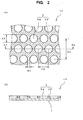
- Fig. 1 is a schematic plane view of the main part of the anode of the lithium secondary battery in preferable embodiment of the present invention ( Fig. 1 (A) ) and a schematic sectional view thereof ( Fig. 1 (B) )
- Fig. 2 is a schematic plane view of the main part of the anode of the lithium secondary battery in the other preferable embodiment of the present invention ( Fig. 2 (A) ) and a schematic sectional view thereof ( Fig. 2 (B) ).
- Fig. 1 (B) shows a sectional view along the line Ib-Ib in Fig. 1 (A)
- Fig. 2 (B) shows a sectional view along the line IIb-IIb in Fig. 2 (A) .
- the current collector layer 1 does not have an opening. As a result, the current collector layer 1 can maintain its electrical resistance at a low level as well as sufficient intensity.
- a network structure has an opening 2A. That is, when the active material layer 2 is seen from the perpendicular direction, plural openings 2A are regularly aligned, and the periphery of the individual openings 2A are covering parts 2B covering the current collector layer 1.
- the regular alignment of the openings 2A in the network structure is zigzag alignment, matrix alignment and the like, with preference given to zigzag alignment.
- openings 2A are aligned in a zigzag manner.
- lithium goes in and out from the active material layer, which causes expansion/contraction of the active material layer.
- the stress due to the expansion/contraction breaks the active material layer, and charge-discharge capacity may sometimes decrease.
- the presence of an opening in the active material layer can prevent breakage of the active material layer due to the expansion/contraction, and can prevent decrease of charge-discharge capacity of the lithium secondary battery.
- the shape of the opening in the active material layer in a planar view is preferably a substantially regular polygon of pentagon or above and/or a substantial circle.
- the "substantially regular polygon” means a polygon wherein the length of the longest side is not more than 1.1 times the length of the shortest side, and includes, besides regular polygons, polygons similar to regular polygons.
- the length of the longest side of a substantially regular polygon is preferably not more than 1.05 times the length of the shortest side, and the substantially regular polygon is more preferably a regular polygon.
- the "substantial circle” means an ellipse or oval wherein the major axis thereof (long axis) is not more than 1.1 times the length of the minor axis (short axis), and includes circles.
- the major axis of the substantial circle is preferably not more than 1.05 times the length of the minor axis, and the substantial circle is more preferably a circle.
- the shape of the opening 2A is a regular hexagon
- Fig. 2 (A) the shape of the opening 2A is a circle.
- the opening in the active material layer is a substantially regular polygon of pentagon or above and/or a substantial circle
- the charge-discharge cycle characteristics of the lithium secondary battery can be improved. While the mechanism thereof is not certain, it is assumed since a substantially regular polygon of pentagon or above has more corners, at which the stress is considered capable of concentrating, the concentration of stress is reduced, and the breakage of the active material layer is further prevented.
- the substantial circle can be considered to have an infinitely increasing number of corners of the substantially regular polygon, and therefore, even a substantial circle is considered to reduce the stress concentration.
- the substantially regular polygon of pentagon or above is preferably a substantially regular hexagon and/or substantially regular octagon, more preferably substantially regular hexagon.
- the shape of the opening in the active material layer is preferably at least one selected from the group comprised of a substantially regular hexagon, a substantially regular octagon and a substantial circle, more preferably a substantially regular hexagon (particularly a regular hexagon) and/or a substantial circle (particularly a circle).
- the shape of the opening is more preferably a substantially regular hexagon (particularly a regular hexagon).
- the shape of the opening in the active material layer be basically a single shape (namely, plural openings have the same shape).
- two or more kinds of openings having different shapes may also be present.
- an opening of a substantially regular hexagon and an opening of a substantial circle may be present, and an opening of a substantially regular hexagon and an opening of a substantially regular octagon may be present.
- the longest distance across the corners of the opening which is a substantially regular polygon (A1 in Fig. 1 (A) ), is preferably not less than 1 ⁇ m, more preferably not less than 50 ⁇ m, still more preferably not less than 100 ⁇ m, and preferably not more than 1000 ⁇ m, more preferably not more than 900 ⁇ m, more preferably not more than 800 ⁇ m.
- the diameter or long axis (A2 in Fig.
- 2 (A) ) of the opening which is a substantial circle, is preferably not less than 1 ⁇ m, more preferably not less than 50 ⁇ m, still more preferably not less than 100 ⁇ m, and preferably not more than 1000 ⁇ m, more preferably not more than 900 ⁇ m, still more preferably not more than 800 ⁇ m.
- the active material layer preferably has uniform property in the entirety thereof.
- the maximum length (maximum distance across corners, or diameter or long axis) of the maximum opening in the active material layer is preferably not more than 2.0 times, more preferably not more than 1.5 times, the maximum length (maximum distance across corners, or diameter or long axis) of the minimum opening, wherein each opening more preferably has substantially the same size. That "each opening has substantially the same size” means the difference in the size of each opening is within the range of production error. In actual production, even if the openings are set to the same size, the size dispersion may occur due to a production error.
- the minimum width of the covering part of the active material layer is preferably not less than 1 ⁇ m, more preferably not less than 10 ⁇ m, still more preferably not less than 20 ⁇ m, and preferably not more than 500 ⁇ m, more preferably not more than 300 ⁇ m, still more preferably not more than 100 ⁇ m.
- the minimum width of the covering part means the smallest distance between adjacent two openings (e.g., B1 in Fig. 1 (A) , B2 in Fig. 2 (A) ).
- the covering rate is preferably not less than 5 area %, more preferably not less than 10 area %, more preferably not less than 15 area %, and preferably not more than 70 area %, more preferably not more than 65 area %, more preferably not more than 60 area %.
- the sheet for the anode of the present invention can be produced by, for example, forming an Ni layer on a copper foil (preferably electrolytic copper foil), then forming an Sn-Cu layer thereon, and heat-treating a copper foil having an Ni layer/Sn-Cu layer.
- the heat treatment causes diffusion and moved metal components, and on the copper foil (Cu layer), a Cu 3 Sn layer and Ni x Cu 6-x Sn 5 layer can be formed in this order.
- the thickness of the Ni layer formed before heat treatment and the like the value of the x in the Ni x Cu 6-x Sn 5 layer can be adjusted.
- Ni layer and Sn-Cu layer examples include electrolytic plating, non-electrolytic plating, sputtering, vapor deposition and the like. Of these, electrolytic plating is preferable.
- the heat treatment temperature of the copper foil having the Ni layer/Sn-Cu layer is preferably not less than the melting point of Sn (232°C), more preferably 235 - 400°C.
- the time of the heat treatment is preferably 0.5 - 50 hr.
- Preferable sheet for the anode of the present invention having the active material layer which forms an opening and has a cancellous structure can be produced by, for example, forming a resist film that formations of an opening and a covering part are turned around the active material layer, on copper foil by photolithography, forming a Ni layer and Sn-Cu layer thereon, then removing the resist film to form a Ni layer/Sn-Cu layer having an opening, and then by heat-treating copper film having this Ni layer/Sn-Cu layer.
- the anode of the present invention can be produced by cutting or punching out a sheet for anode produced as mentioned above to a desired size by a known means.
- the present invention further provides a lithium secondary battery containing the above-mentioned anode.
- the lithium secondary battery of the present invention characteristically contains the above-mentioned anode, and other constitution is not particularly limited.
- the constitution of the lithium secondary battery and the production method thereof are known and are described, for example, in patent documents 1 and 2 and the like. Examples
- a negative resist film (thickness: 25 ⁇ m) was laminated on an electrolytic copper foil (thickness: 20 ⁇ m).
- an electrolytic copper foil (thickness: 20 ⁇ m).
- the resist film was exposed and developed to form a developed resist film (shape of covering part: regular hexagon) with a pattern inverted to the photomask.
- An electrolytic copper foil having a development resist film was immersed in a plating solution (aqueous solution containing nickel sulfate (NiSO 4 ⁇ 6H 2 O): 300 g/L, nickel chloride (NiCl 2 ⁇ 6H 2 O): 50 g/L, boric acid: 40 g/L) to allow electrolytic plating to form an electrolytic copper foil having an Ni plated layer.
- the electrolytic plating was performed by adjusting the temperature of the plating solution to 50°C, and at a current density of 1 A/dm 2 .
- the electrolytic copper foil having the Ni plated layer obtained as mentioned above was immersed in a plating solution (aqueous solution containing tin(II) methanesulfonate: 39 g/L, copper(II) methanesulfonate: 6.6 g/L, methanesulfonic acid: 100 g/L, bisphenol: 5 g/L, thiourea: 10 g/L, catechol 1 g/L), and electroplating was carried out to form an Sn-Cu eutectoid plated layer (thickness: 10 ⁇ m) on the Ni plated layer.
- a plating solution aqueous solution containing tin(II) methanesulfonate: 39 g/L, copper(II) methanesulfonate: 6.6 g/L, methanesulfonic acid: 100 g/L, bisphenol: 5 g/L, thiourea: 10 g/L, catechol
- This electroplating was carried out while adjusting the temperature of the plating solution to 40°C for 20 min at current density of 1 A/dm 2 .
- the electrolytic copper foil having the Sn-Cu eutectoid plated layer was washed with water, and the developed resist film was detached with 3 - 5 wt% NaOH aqueous solution and further washed with water to give an electrolytic copper foil (current collector layer) having the Ni plated layer/the Sn-Cu eutectoid plated layer, wherein regular hexagon openings were aligned in a zigzag manner.
- the electrolytic copper foil having the Ni plated layer/Sn-Cu eutectoid plated layer obtained as mentioned above was heat-treated at 250°C for 5 hr under the atmosphere to give a sheet for an anode, which has a Cu 3 Sn layer and an Ni x Cu 6-x Sn 5 layer in this order (A1: 0.30 mm, B1: 0.046 mm, C1: 0.30 mm, D1: 0.52 mm, covering rate: 29 area%) as active material layers shown in Fig. 1(A) , on a current collector layer (electrolytic copper foil).
- the size of each part of the active material layer was calculated from an electron micrograph taken by an electron microscope: "JSM-6390A" manufactured by JEOL.
- the sheets for anode produced in Examples 1 - 4 and Comparative Examples 1 and 2 were punched out in 16 mm ⁇ in size, and anodes for evaluation were prepared.
- the anodes were dried at 70°C for 1 hr under vacuum, and transferred into a glove box under an argon atmosphere. Under an argon atmosphere in the glove box, a 2016 size-coin cell type battery was produced using the anode.
- a sheet for a cathode a sheet having an aluminum foil as a current collector layer and lithium cobalt dioxide as an active material layer was used, and this was punched out in 15 mm ⁇ and used as another side (cathode) of the battery.
- the battery produced as mentioned above was placed in a thermostat at 25°C, and charged and discharged 60 cycles in total at the following charge-discharge rates.
- Table 1 also describes the thicknesses of the Ni plated layer and Sn-Cueutectoid plated layer formed before a heat treatment, the thickness of the Cu 3 Sn layer formed after a heat treatment, the thickness of the Ni x Cu 6-x Sn 5 layer and the value of x.
- the thickness of the Ni plated layer, Sn-Cu eutectoid plated layer, Cu 3 Sn layer and Ni x Cu 6-x Sn 5 layer described in Table 1 was determined by performing FIB microsampling at accelerating voltage 40 kV using Hitachi FB-2100, taking a sectional SEM image of the sample by FE-SEM (manufactured by Joel, JSM-7001F, accelerating voltage 15 kV), and calculating the thickness from the image.
- the value of x was measured by calculating the ratio of each element of the Ni x Cu 6-x Sn 5 layer by elemental analysis using Field Emission Scanning Electron Microscope-X-ray Micro Analyzer (FE-SEM-XMA) (FE-SEM (manufactured by Joel, JSM-7001F, accelerating voltage 15 kV), XMA (manufactured by Oxford Instruments, Inca Energy 250, energy dispersion type)), and calculating from the ratio.
- FE-SEM-XMA Field Emission Scanning Electron Microscope-X-ray Micro Analyzer
- the batteries using the anode of the present invention (Examples 1 - 4) having an Ni x Cu 6-x Sn 5 layer (x is 0.30 - 2.0) show superior relative discharged capacity as compared to the anode having an Ni x Cu 6-x Sn 5 layer (x is less than 0.30) (Comparative Example 1) and the anode having an Ni x Cu 6-x Sn 5 layer (x is more than 2.0) (Comparative Example 2).
Landscapes
- Chemical & Material Sciences (AREA)
- Chemical Kinetics & Catalysis (AREA)
- Electrochemistry (AREA)
- General Chemical & Material Sciences (AREA)
- Engineering & Computer Science (AREA)
- Materials Engineering (AREA)
- Composite Materials (AREA)
- Manufacturing & Machinery (AREA)
- Cell Electrode Carriers And Collectors (AREA)
- Battery Electrode And Active Subsutance (AREA)
Abstract
Description
- The present invention relates to a component for a lithium secondary battery, an anode of a lithium secondary battery, and a lithium secondary battery. The present invention also relates to a sheet useful for producing an anode of a lithium secondary battery (i.e., sheet for anode of lithium secondary battery).
- An anode of a lithium secondary battery comprises a current collector (e.g., copper foil) and an active material layer laminated on the current collector. As such active material, various materials have been proposed heretofore. For example,
JP-A-2004-103474 JP-A-H11-233116 - The performance of an anode of conventional lithium secondary batteries to prevent decrease of the charge and discharge capacity due to repeated charge and discharge cycle (hereinafter abbreviated as "charge-discharge cycle characteristics") is not sufficient. It is therefore an object of the present invention to provide an anode of a lithium secondary battery, which can achieve a charge-discharge cycle characteristics superior to that of the prior art.
- The present inventors have conducted intensive studies in an attempt to achieve the above-mentioned object and completed the following invention.
- [1] An anode of a lithium secondary battery comprising a current collector layer and an active material layer laminated on the current collector layer, wherein the active material layer has a layer comprised of NixCu6-xSn5 (x is 0.30 - 2.0).
- [2] The anode of the above-mentioned [1], wherein the active material layer further has a layer comprised of Cu3Sn, which is present between a current collector layer and a layer comprised of NixCu6-xSn5 (x is 0.30 - 2.0).
- [3] The anode of the above-mentioned [2], wherein the current collector layer is a copper foil.
- [4] The anode of any one of the above-mentioned [1] - [3], wherein the current collector layer has a laminar structure without an opening, and the active material layer has a network structure with an opening.
- [5] The anode of the above-mentioned [4], wherein the shape of the opening in a planar view is a substantially regular polygon of pentagon or above and/or a substantial circle.
- [6] The anode of the above-mentioned [5], wherein the shape of the opening in a planar view is a substantially regular polygon of hexagon.
- [7] A lithium secondary battery comprising the anode of any one of the above-mentioned [1] - [6].
- [8] A sheet for an anode of a lithium secondary battery comprising a current collector layer and an active material layer laminated on the current collector layer, wherein the active material layer has a layer comprised of NixCu6-xSn5 (x is 0.30 - 2.0).
- In the following, the "layer comprised of NixCu6-xSn5" and "layer comprised of Cu3Sn" are sometimes to be abbreviated as "NixCu6-xSn5 layer" and "Cu3Sn layer", respectively.
In addition, in the present invention, the "opening of the active material layer" means a part free of an active material, and the "shape of the opening in a planar view" means a shape of the opening when the active material layer is seen from the perpendicular direction. Moreover, a "network structure having an opening" in the active material layer means that, when the active material layer is seen from the perpendicular direction, plural openings are regularly aligned, and the periphery of the individual openings form a part covering the current collector layer (part where active material is present). - Using the anode of the present invention, a lithium secondary battery superior in the charge-discharge cycle characteristics can be produced.
-
-
Fig. 1 (A) is a schematic plane view of the main part of the anode of the lithium secondary battery in preferable embodiment of the present invention, andFig. 1 (B) is a schematic sectional view along the line Ib-Ib ofFig. 1 (A) . -
Fig. 2 (A) is a schematic plane view of the main part of the anode of the lithium secondary battery in the other preferable embodiment of the present invention, andFig. 2 (B) is a schematic sectional view along the line IIb-IIb ofFig. 2 (A) . -
Fig. 3 is a schematic plane view of the photomask used in Examples 1 - 4 and Comparative Examples 1 and 2. - The present invention relates to an anode of a lithium secondary battery and a sheet for the anode. In the present invention, "a sheet for an anode of a lithium secondary battery" is a sheet used for producing "an anode of a lithium secondary battery", and "an anode of a lithium secondary battery" can be produced by cutting or punching out this sheet in a desired size. In the following description, therefore, "anode" is used to show a concept encompassing an anode of a lithium secondary battery and a sheet for the anode, unless particularly specified.
- The anode of the present invention has a current collector layer and an active material layer laminated on the current collector layer, wherein the active material layer has an NixCu6-xSn5 layer (x is 0.30 - 2.0). The active material layer may be formed only on one surface of the current collector layer, or may be formed on both surfaces of the current collector layer.
- The superior charge-discharge cycle characteristic of the anode of the present invention is considered to be attributable to the presence of an NixCu6-xSn5 layer comprised of Cu6Sn5 containing an appropriate amount of Ni (x is 0.30 - 2.0), since it can prevent the active material layer from falling off due to charge-discharge of the battery. However, the present invention is not limited to such assumption. The value of x is preferably 0.4 - 1.8, more preferably 0.6 - 1.5. The value of x can be measured and calculated by the method described in the Examples mentioned below.
- The thickness of the NixCu6-xSn5 layer (x is 0.30 - 2.0) is preferably not less than 0.1 µm, more preferably not less than 1 µm, preferably not more than 100 µm, more preferably not more than 50 µm. When the NixCu6-xSn5 layer is too thin, sufficient capacity as a battery may not be obtained. On the other hand, when the NixCu6-xSn5 layer is too thick, diffusion of Li to the depth of the layer takes time, and an electric current practical for a battery may not be obtained. The thickness of the NixCu6-xSn5 layer can be measured by the method described in the Examples mentioned below.
- In the anode of the present invention, the active material layer preferably further has a Cu3Sn layer, and the active material layer more preferably consists of an NixCu6-xSn5 layer (x is 0.30 - 2.0) and a Cu3Sn layer. The Cu3Sn layer is present between the current collector layer and the NixCu6-xSn5 layer.
- When the Cu3Sn layer is present, the thickness thereof is preferably not less than 0.5 µm, more preferably not less than 1 µm, further preferably not more than 10 µm, still more preferably not more than 5 µm. The Cu3Sn layer is considered to function as a stress relaxing layer for the NixCu6-xSn5 layer and the current collector. When the Cu3Sn layer is too thin, the effect of stress relaxation cannot be obtained sufficiently, and the charge-discharge cycle characteristic may not be sufficiently high. On the other hand, when the Cu3Sn layer is too thick, the part that can be alloyed with Li becomes relatively small, and the energy density of the battery may decrease. The thickness of the Cu3Sn layer can be measured by the method described in the Example mentioned below.
- The current collector layer is generally formed from a metal or alloy having conductivity. Preferred is a metal foil or an alloy foil,'more preferred is a copper foil, and further preferred is an electrolytic copper foil. The thickness of the current collector layer is preferably not less than 1 µm, more preferably not less than 5 µm, further preferably not less than 8 µm, preferably not more than 50 µm, more preferably not more than 30 µm, further preferably not more than 20 µm. When the current collector layer is too thin, the internal resistance of the battery becomes high, and load characteristic of the battery decreases. On the other hand, when the current collector layer is too thick, the volume and weight of the battery become high, and the energy density decreases.
- In the anode of the present invention, the current collector layer has a layer structure free of an opening, and the active material layer preferably has a cancellous structure with an opening. Preferable embodiments of the present invention are explained in the following by referring to
Figs. 1 and2 . -
Fig. 1 is a schematic plane view of the main part of the anode of the lithium secondary battery in preferable embodiment of the present invention (Fig. 1 (A) ) and a schematic sectional view thereof (Fig. 1 (B) ),Fig. 2 is a schematic plane view of the main part of the anode of the lithium secondary battery in the other preferable embodiment of the present invention (Fig. 2 (A) ) and a schematic sectional view thereof (Fig. 2 (B) ).Fig. 1 (B) shows a sectional view along the line Ib-Ib inFig. 1 (A) , andFig. 2 (B) shows a sectional view along the line IIb-IIb inFig. 2 (A) . - In the preferable embodiment of the present invention, the
current collector layer 1 does not have an opening. As a result, thecurrent collector layer 1 can maintain its electrical resistance at a low level as well as sufficient intensity. - In the
active material layer 2, a network structure has anopening 2A. That is, when theactive material layer 2 is seen from the perpendicular direction,plural openings 2A are regularly aligned, and the periphery of theindividual openings 2A are covering parts 2B covering thecurrent collector layer 1. Typically, the regular alignment of theopenings 2A in the network structure is zigzag alignment, matrix alignment and the like, with preference given to zigzag alignment. InFig. 1 (A) andFig. 2 (A) ,openings 2A are aligned in a zigzag manner. - During charge-discharge of a lithium secondary battery, lithium goes in and out from the active material layer, which causes expansion/contraction of the active material layer. The stress due to the expansion/contraction breaks the active material layer, and charge-discharge capacity may sometimes decrease. On this point, the presence of an opening in the active material layer can prevent breakage of the active material layer due to the expansion/contraction, and can prevent decrease of charge-discharge capacity of the lithium secondary battery.
- The shape of the opening in the active material layer in a planar view is preferably a substantially regular polygon of pentagon or above and/or a substantial circle. In the present invention, the "substantially regular polygon" means a polygon wherein the length of the longest side is not more than 1.1 times the length of the shortest side, and includes, besides regular polygons, polygons similar to regular polygons. The length of the longest side of a substantially regular polygon is preferably not more than 1.05 times the length of the shortest side, and the substantially regular polygon is more preferably a regular polygon. The "substantial circle" means an ellipse or oval wherein the major axis thereof (long axis) is not more than 1.1 times the length of the minor axis (short axis), and includes circles. The major axis of the substantial circle is preferably not more than 1.05 times the length of the minor axis, and the substantial circle is more preferably a circle. In
Fig. 1 (A) , the shape of theopening 2A is a regular hexagon, and inFig. 2 (A) , the shape of theopening 2A is a circle. - When the opening in the active material layer is a substantially regular polygon of pentagon or above and/or a substantial circle, the charge-discharge cycle characteristics of the lithium secondary battery can be improved. While the mechanism thereof is not certain, it is assumed since a substantially regular polygon of pentagon or above has more corners, at which the stress is considered capable of concentrating, the concentration of stress is reduced, and the breakage of the active material layer is further prevented. The substantial circle can be considered to have an infinitely increasing number of corners of the substantially regular polygon, and therefore, even a substantial circle is considered to reduce the stress concentration. However, the present invention is not limited to the presumed mechanism. The substantially regular polygon of pentagon or above is preferably a substantially regular hexagon and/or substantially regular octagon, more preferably substantially regular hexagon.
- The shape of the opening in the active material layer is preferably at least one selected from the group comprised of a substantially regular hexagon, a substantially regular octagon and a substantial circle, more preferably a substantially regular hexagon (particularly a regular hexagon) and/or a substantial circle (particularly a circle). The shape of the opening is more preferably a substantially regular hexagon (particularly a regular hexagon). When the opening of the active material layer is a substantial circle, as shown in
Fig. 2 (A) , the width of the covering part 2B on the periphery ofopening 2A is not uniform, including a wide part and a narrow part. When the opening is a substantially regular hexagon, as shown inFig. 1 (A) , the width of the covering part 2B on the periphery ofopening 2A is almost uniform, which enables formation of anactive material layer 2 having superior intensity. - It is preferable that the shape of the opening in the active material layer be basically a single shape (namely, plural openings have the same shape). However, two or more kinds of openings having different shapes may also be present. For example, an opening of a substantially regular hexagon and an opening of a substantial circle may be present, and an opening of a substantially regular hexagon and an opening of a substantially regular octagon may be present.
- When the size of the opening in the active material layer is too small, the stress due to expansion/contraction of the active material layer cannot be alleviated sufficiently. When the size of the opening is too large, charge and discharge capacity of a lithium secondary battery becomes too small. The longest distance across the corners of the opening, which is a substantially regular polygon (A1 in
Fig. 1 (A) ), is preferably not less than 1 µm, more preferably not less than 50 µm, still more preferably not less than 100 µm, and preferably not more than 1000 µm, more preferably not more than 900 µm, more preferably not more than 800 µm. In addition, the diameter or long axis (A2 inFig. 2 (A) ) of the opening, which is a substantial circle, is preferably not less than 1 µm, more preferably not less than 50 µm, still more preferably not less than 100 µm, and preferably not more than 1000 µm, more preferably not more than 900 µm, still more preferably not more than 800 µm. - While the size of each opening in the active material layer may be different, the active material layer preferably has uniform property in the entirety thereof. Thus, the maximum length (maximum distance across corners, or diameter or long axis) of the maximum opening in the active material layer is preferably not more than 2.0 times, more preferably not more than 1.5 times, the maximum length (maximum distance across corners, or diameter or long axis) of the minimum opening, wherein each opening more preferably has substantially the same size. That "each opening has substantially the same size" means the difference in the size of each opening is within the range of production error. In actual production, even if the openings are set to the same size, the size dispersion may occur due to a production error.
- When the minimum width of the covering part of the active material layer is too small, the active material layer does not adhere sufficiently to the current collector layer, and the active material may drop off after repeated charge and discharge cycles. On the other hand, when the minimum width of the covering part is too large, the stress caused by expansion/contraction of the active material layer cannot be reduced sufficiently. Therefore, the minimum width of the covering part is preferably not less than 1 µm, more preferably not less than 10 µm, still more preferably not less than 20 µm, and preferably not more than 500 µm, more preferably not more than 300 µm, still more preferably not more than 100 µm. Here, "the minimum width of the covering part" means the smallest distance between adjacent two openings (e.g., B1 in
Fig. 1 (A) , B2 inFig. 2 (A) ). - When, in the active material layer, the area ratio of the covering part relative to the total area including opening and covering part (hereinafter sometimes to be abbreviated as "covering rate") is too small, the charge and discharge capacity of the lithium secondary battery becomes too small. On the other hand, when it is too high, the stress caused by expansion/contraction of the active material layer cannot be reduced sufficiently. Hence, the covering rate is preferably not less than 5 area %, more preferably not less than 10 area %, more preferably not less than 15 area %, and preferably not more than 70 area %, more preferably not more than 65 area %, more preferably not more than 60 area %.
- The sheet for the anode of the present invention can be produced by, for example, forming an Ni layer on a copper foil (preferably electrolytic copper foil), then forming an Sn-Cu layer thereon, and heat-treating a copper foil having an Ni layer/Sn-Cu layer. The heat treatment causes diffusion and moved metal components, and on the copper foil (Cu layer), a Cu3Sn layer and NixCu6-xSn5 layer can be formed in this order. By adjusting the thickness of the Ni layer formed before heat treatment and the like, the value of the x in the NixCu6-xSn5 layer can be adjusted.
- Examples of the formation method of Ni layer and Sn-Cu layer include electrolytic plating, non-electrolytic plating, sputtering, vapor deposition and the like. Of these, electrolytic plating is preferable. The heat treatment temperature of the copper foil having the Ni layer/Sn-Cu layer is preferably not less than the melting point of Sn (232°C), more preferably 235 - 400°C. The time of the heat treatment is preferably 0.5 - 50 hr.
- Preferable sheet for the anode of the present invention having the active material layer which forms an opening and has a cancellous structure can be produced by, for example, forming a resist film that formations of an opening and a covering part are turned around the active material layer, on copper foil by photolithography, forming a Ni layer and Sn-Cu layer thereon, then removing the resist film to form a Ni layer/Sn-Cu layer having an opening, and then by heat-treating copper film having this Ni layer/Sn-Cu layer.
- The anode of the present invention can be produced by cutting or punching out a sheet for anode produced as mentioned above to a desired size by a known means.
- The present invention further provides a lithium secondary battery containing the above-mentioned anode. The lithium secondary battery of the present invention characteristically contains the above-mentioned anode, and other constitution is not particularly limited. The constitution of the lithium secondary battery and the production method thereof are known and are described, for example, in
patent documents - The present invention is explained in more detail in the following by referring to Examples. However, the present invention is not limited to the following Examples, and can be practiced by making appropriate modifications and changes without substantially departing from the above or below-mentioned teaching and advantages of the present invention, all of which are encompassed in the technical scope of the present invention.
- A negative resist film (thickness: 25 µm) was laminated on an electrolytic copper foil (thickness: 20 µm). Using a photomask of the shape shown in
Fig. 3 (inFig. 3 , symbol 3 shows a translucent part, andsymbol 4 shows a light shielding part, a1: 0.30 mm, b1: 0.05 mm, c1: 0.31 mm, d1: 0.54 mm), the resist film was exposed and developed to form a developed resist film (shape of covering part: regular hexagon) with a pattern inverted to the photomask. - An electrolytic copper foil having a development resist film was immersed in a plating solution (aqueous solution containing nickel sulfate (NiSO4·6H2O): 300 g/L, nickel chloride (NiCl2·6H2O): 50 g/L, boric acid: 40 g/L) to allow electrolytic plating to form an electrolytic copper foil having an Ni plated layer. The electrolytic plating was performed by adjusting the temperature of the plating solution to 50°C, and at a current density of 1 A/dm2. The thickness of the Ni plated layer was adjusted by the plating time. Specifically, the electrolytic plating was performed for 5 min to form an Ni plated layer having a thickness of 1 µm (thickness of Ni plated layer/plating time=0.2 µm/min).
- The electrolytic copper foil having the Ni plated layer obtained as mentioned above was immersed in a plating solution (aqueous solution containing tin(II) methanesulfonate: 39 g/L, copper(II) methanesulfonate: 6.6 g/L, methanesulfonic acid: 100 g/L, bisphenol: 5 g/L, thiourea: 10 g/L, catechol 1 g/L), and electroplating was carried out to form an Sn-Cu eutectoid plated layer (thickness: 10 µm) on the Ni plated layer. This electroplating was carried out while adjusting the temperature of the plating solution to 40°C for 20 min at current density of 1 A/dm2. The electrolytic copper foil having the Sn-Cu eutectoid plated layer was washed with water, and the developed resist film was detached with 3 - 5 wt% NaOH aqueous solution and further washed with water to give an electrolytic copper foil (current collector layer) having the Ni plated layer/the Sn-Cu eutectoid plated layer, wherein regular hexagon openings were aligned in a zigzag manner.
- The electrolytic copper foil having the Ni plated layer/Sn-Cu eutectoid plated layer obtained as mentioned above was heat-treated at 250°C for 5 hr under the atmosphere to give a sheet for an anode, which has a Cu3Sn layer and an NixCu6-xSn5 layer in this order (A1: 0.30 mm, B1: 0.046 mm, C1: 0.30 mm, D1: 0.52 mm, covering rate: 29 area%) as active material layers shown in
Fig. 1(A) , on a current collector layer (electrolytic copper foil). The size of each part of the active material layer was calculated from an electron micrograph taken by an electron microscope: "JSM-6390A" manufactured by JEOL. - The sheets for anode produced in Examples 1 - 4 and Comparative Examples 1 and 2 were punched out in 16 mmϕ in size, and anodes for evaluation were prepared. The anodes were dried at 70°C for 1 hr under vacuum, and transferred into a glove box under an argon atmosphere. Under an argon atmosphere in the glove box, a 2016 size-coin cell type battery was produced using the anode. As a sheet for a cathode, a sheet having an aluminum foil as a current collector layer and lithium cobalt dioxide as an active material layer was used, and this was punched out in 15 mmφ and used as another side (cathode) of the battery. In addition, as a separator, a fine porous film made of polyethylene (thickness: 25 µm, porosity: 40% by volume, average diameter of void: 0.1 µm) was used and, as an electrolytic solution, a 1.4M LiPF6 solution (solvent: ethylene carbonate (EC) and diethyl carbonate (DEC), volume ratio of EC:DEC = 1:2) was used.
- The battery produced as mentioned above was placed in a thermostat at 25°C, and charged and discharged 60 cycles in total at the following charge-discharge rates.
- (i) 1 time of 5 cycles at 0.2 CmA charge-discharge rate (total 5 cycles)
- (ii) 5 times of a combination of 10 cycles at 1 CmA charge-discharge rate, and then 1 cycle at 0.2 CmA charge-discharge rate (total 55 cycles)
- In the above-mentioned charge-discharge at 0.2 CmA charge-discharge rate, constant electric current and voltage charging at charge upper limit voltage of 4.0 V and charge completion time of 7 hr was performed (that is, charging to battery voltage of 4.0 V, followed by charging for 7 hr at controlled electric current to maintain the battery voltage of 4.0 V), and constant electric current discharging was performed at discharge completion voltage of 2.5 V (that is, discharging at constant electric current until battery voltage became 2.5 V). A break time for 30 min was set between charging and discharging.
- In the above-mentioned charge-discharge at charge-discharge rate of 1 CmA, constant electric current and voltage charging at charge upper limit voltage of 4.0 V and charge completion time of 2 hr was performed, and constant electric current discharging was performed at discharge completion voltage of 2.5 V. A break time for 30 min was set between charging and discharging.
- The charge-discharge cycle test was performed as mentioned above, the discharged capacity at the first cycle and the discharged capacity at the 60th cycle were measured, and relative discharged capacity (=100 x discharged capacity at 60th cycles/discharged capacity at the first cycle) was calculated. The results of the relative discharged capacity are shown in Table 1.
- Table 1 also describes the thicknesses of the Ni plated layer and Sn-Cueutectoid plated layer formed before a heat treatment, the thickness of the Cu3Sn layer formed after a heat treatment, the thickness of the NixCu6-xSn5 layer and the value of x.
- The thickness of the Ni plated layer, Sn-Cu eutectoid plated layer, Cu3Sn layer and NixCu6-xSn5 layer described in Table 1 was determined by performing FIB microsampling at accelerating voltage 40 kV using Hitachi FB-2100, taking a sectional SEM image of the sample by FE-SEM (manufactured by Joel, JSM-7001F, accelerating voltage 15 kV), and calculating the thickness from the image. In addition, the value of x was measured by calculating the ratio of each element of the NixCu6-xSn5 layer by elemental analysis using Field Emission Scanning Electron Microscope-X-ray Micro Analyzer (FE-SEM-XMA) (FE-SEM (manufactured by Joel, JSM-7001F, accelerating voltage 15 kV), XMA (manufactured by Oxford Instruments, Inca Energy 250, energy dispersion type)), and calculating from the ratio.
-
Table 1 before heat treatment after heat treatment relative dis-harge capacity Ni plated layer Sn-Cu eutectoid plated layer Cu3Sn layer NixCu6-xSn5 layer thickness (µm) thickness (µm) thickness (µm) thickness (µm) x value Ex.1 0.25 10 3.0 10 0.46 91 Ex.2 0.5 10 3.3 10 0.74 96 Ex.3 0.75 10 3.5 10 1.0 95 Ex.4 1.0 10 4.0 10 1.8 90 Com. Ex.1 0.1 10 2.0 10 0.28 72 Com. Ex.2 1.5 10 4.0 12 2.2 76 current collector layer: electrolytic copper foil
active material layers: Cu3Sn layer and NixCu6-xSn5 layer - As is clear from Table 1, the batteries using the anode of the present invention (Examples 1 - 4) having an NixCu6-xSn5 layer (x is 0.30 - 2.0) show superior relative discharged capacity as compared to the anode having an NixCu6-xSn5 layer (x is less than 0.30) (Comparative Example 1) and the anode having an NixCu6-xSn5 layer (x is more than 2.0) (Comparative Example 2).
Claims (9)
- A component for a lithium secondary battery comprising a current collector layer and an active material layer laminated on the current collector layer, wherein the active material layer has a layer comprised of NixCu6-xSn5 (x is 0.30 - 2.0).
- The component according to claim 1, wherein the active material layer further has a layer comprised of Cu3Sn, which is present between a current collector layer and a layer comprised of NixCu6-xSn5 (x is 0.30 - 2.0).
- The component according to claim 2, wherein the current collector layer is a copper foil.
- The component according to any one of claims 1 to 3, wherein the current collector layer has a laminar structure without an opening, and the active material layer has a network structure with an opening.
- The component according to claim 4, wherein the shape of the opening in a planar view is a substantially regular polygon of pentagon or above and/or a substantial circle.
- The component according to claim 5, wherein the shape of the opening in a planar view is a substantially regular polygon of hexagon.
- The component according to any one of claims 1 to 6, wherein the component is an anode of said lithium secondary battery.
- A lithium secondary battery comprising the anode according to claim 7.
- The component according to any one of claims 1 to 6, wherein the component is a sheet for an anode of said lithium secondary battery.
Applications Claiming Priority (1)
| Application Number | Priority Date | Filing Date | Title |
|---|---|---|---|
| JP2011173808A JP5780880B2 (en) | 2011-08-09 | 2011-08-09 | Lithium secondary battery and negative electrode thereof |
Publications (2)
| Publication Number | Publication Date |
|---|---|
| EP2557617A1 true EP2557617A1 (en) | 2013-02-13 |
| EP2557617B1 EP2557617B1 (en) | 2014-05-14 |
Family
ID=46651421
Family Applications (1)
| Application Number | Title | Priority Date | Filing Date |
|---|---|---|---|
| EP12179917.5A Not-in-force EP2557617B1 (en) | 2011-08-09 | 2012-08-09 | Lithium secondary battery and anode therefor |
Country Status (5)
| Country | Link |
|---|---|
| US (1) | US20130040200A1 (en) |
| EP (1) | EP2557617B1 (en) |
| JP (1) | JP5780880B2 (en) |
| KR (1) | KR20130018606A (en) |
| CN (1) | CN102931382A (en) |
Cited By (1)
| Publication number | Priority date | Publication date | Assignee | Title |
|---|---|---|---|---|
| US11383315B2 (en) | 2019-02-01 | 2022-07-12 | Vacuumschmelze Gmbh & Co. Kg | Method for pre-treating stainless steel substrates before soldering using nanocrystalline solder foils |
Families Citing this family (8)
| Publication number | Priority date | Publication date | Assignee | Title |
|---|---|---|---|---|
| DE102013204863A1 (en) * | 2013-03-20 | 2014-09-25 | Robert Bosch Gmbh | Electrode and method for manufacturing an electrode |
| US9761861B1 (en) | 2013-06-25 | 2017-09-12 | Quantumscape Corporation | Pulse plating of lithium material in electrochemical devices |
| KR101660111B1 (en) * | 2014-07-18 | 2016-09-26 | 주식회사 엘지화학 | Lithium secondary battery electrode and method for preparing the same |
| US10116003B2 (en) * | 2015-02-03 | 2018-10-30 | Quantumscape Corporation | Metal sulfide anolytes for electrochemical cells |
| CN106876688B (en) * | 2015-12-10 | 2020-12-01 | 中国科学院大连化学物理研究所 | A kind of lithium ion battery tin-based alloy negative electrode material and preparation method thereof |
| JP6745782B2 (en) * | 2017-01-26 | 2020-08-26 | 本田技研工業株式会社 | Negative electrode for lithium-ion secondary battery and lithium-ion secondary battery |
| WO2018165606A1 (en) | 2017-03-10 | 2018-09-13 | Quantumscape Corporation | Metal negative electrode ultrasonic charging |
| JP7377427B2 (en) * | 2019-01-31 | 2023-11-10 | 株式会社日本スペリア社 | Negative electrode material for lithium ion secondary battery and its manufacturing method |
Citations (10)
| Publication number | Priority date | Publication date | Assignee | Title |
|---|---|---|---|---|
| JPH11233116A (en) | 1998-02-16 | 1999-08-27 | Canon Inc | Electrode structure for lithium secondary battery, method for manufacturing the same, and lithium secondary battery |
| US20020064704A1 (en) * | 2000-11-10 | 2002-05-30 | Thackeray Michael M. | Intermetallic negative electrodes for non-aqueous lithium cells and batteries |
| JP2003157833A (en) * | 2001-11-19 | 2003-05-30 | Daiwa Kasei Kenkyusho:Kk | Negative electrode for lithium secondary battery and method for producing the same |
| JP2004103474A (en) | 2002-09-11 | 2004-04-02 | Sony Corp | Nonaqueous electrolyte battery and method of manufacturing the same |
| JP2004220871A (en) * | 2003-01-10 | 2004-08-05 | Kobe Steel Ltd | Material of lithium cell anode and its manufacturing method |
| US20050058906A1 (en) * | 2003-09-17 | 2005-03-17 | Hitachi Maxell, Ltd. | Electrode for non-aqueous secondary battery and non-aqueous secondary battery using the same |
| JP2007087789A (en) * | 2005-09-22 | 2007-04-05 | Hitachi Cable Ltd | Negative electrode for lithium ion secondary battery and method for producing the same |
| JP2007250510A (en) * | 2006-02-15 | 2007-09-27 | Sanyo Electric Co Ltd | Electrode for lithium secondary battery and lithium secondary battery |
| JP2009283248A (en) * | 2008-05-21 | 2009-12-03 | Toyota Motor Corp | Negative electrode for nonaqueous electrolyte secondary battery and its manufacturing method |
| EP2432057A1 (en) * | 2010-09-17 | 2012-03-21 | Nitto Denko Corporation | Lithium secondary battery and anode therefor |
Family Cites Families (6)
| Publication number | Priority date | Publication date | Assignee | Title |
|---|---|---|---|---|
| JP3877262B2 (en) * | 1999-09-22 | 2007-02-07 | 株式会社荏原製作所 | Organic wastewater treatment method and equipment |
| JP3877170B2 (en) * | 2003-03-28 | 2007-02-07 | 日立マクセル株式会社 | Non-aqueous secondary battery negative electrode, method for producing the same, and non-aqueous secondary battery using the negative electrode |
| US7507502B2 (en) * | 2003-03-28 | 2009-03-24 | Hitachi Maxell, Ltd. | Negative electrode having intermetallic compound that occludes/desorbs lithium as an active material layer on collector for non-aqueous secondary battery and non-aqueous secondary battery using the same |
| JP4974450B2 (en) * | 2003-09-17 | 2012-07-11 | 日立マクセルエナジー株式会社 | Nonaqueous secondary battery electrode and nonaqueous secondary battery |
| JP2007026963A (en) * | 2005-07-19 | 2007-02-01 | Mitsui Mining & Smelting Co Ltd | Manufacturing method of negative electrode for nonaqueous electrolyte secondary battery |
| WO2010055863A1 (en) * | 2008-11-11 | 2010-05-20 | 株式会社エヌエステクノ | Negative electrode structure for lithium ion secondary battery, and method for producing same |
-
2011
- 2011-08-09 JP JP2011173808A patent/JP5780880B2/en not_active Expired - Fee Related
-
2012
- 2012-08-08 KR KR1020120086656A patent/KR20130018606A/en not_active Withdrawn
- 2012-08-08 US US13/569,857 patent/US20130040200A1/en not_active Abandoned
- 2012-08-09 CN CN2012102827096A patent/CN102931382A/en active Pending
- 2012-08-09 EP EP12179917.5A patent/EP2557617B1/en not_active Not-in-force
Patent Citations (10)
| Publication number | Priority date | Publication date | Assignee | Title |
|---|---|---|---|---|
| JPH11233116A (en) | 1998-02-16 | 1999-08-27 | Canon Inc | Electrode structure for lithium secondary battery, method for manufacturing the same, and lithium secondary battery |
| US20020064704A1 (en) * | 2000-11-10 | 2002-05-30 | Thackeray Michael M. | Intermetallic negative electrodes for non-aqueous lithium cells and batteries |
| JP2003157833A (en) * | 2001-11-19 | 2003-05-30 | Daiwa Kasei Kenkyusho:Kk | Negative electrode for lithium secondary battery and method for producing the same |
| JP2004103474A (en) | 2002-09-11 | 2004-04-02 | Sony Corp | Nonaqueous electrolyte battery and method of manufacturing the same |
| JP2004220871A (en) * | 2003-01-10 | 2004-08-05 | Kobe Steel Ltd | Material of lithium cell anode and its manufacturing method |
| US20050058906A1 (en) * | 2003-09-17 | 2005-03-17 | Hitachi Maxell, Ltd. | Electrode for non-aqueous secondary battery and non-aqueous secondary battery using the same |
| JP2007087789A (en) * | 2005-09-22 | 2007-04-05 | Hitachi Cable Ltd | Negative electrode for lithium ion secondary battery and method for producing the same |
| JP2007250510A (en) * | 2006-02-15 | 2007-09-27 | Sanyo Electric Co Ltd | Electrode for lithium secondary battery and lithium secondary battery |
| JP2009283248A (en) * | 2008-05-21 | 2009-12-03 | Toyota Motor Corp | Negative electrode for nonaqueous electrolyte secondary battery and its manufacturing method |
| EP2432057A1 (en) * | 2010-09-17 | 2012-03-21 | Nitto Denko Corporation | Lithium secondary battery and anode therefor |
Non-Patent Citations (1)
| Title |
|---|
| ZHANG ET AL: "NixCu6-xSn5 alloys as negative electrode materials for rechargeable lithium batteries", JOURNAL OF POWER SOURCES, ELSEVIER SA, CH, vol. 167, no. 1, 4 April 2007 (2007-04-04), pages 171 - 177, XP022016392, ISSN: 0378-7753, DOI: 10.1016/J.JPOWSOUR.2007.02.012 * |
Cited By (2)
| Publication number | Priority date | Publication date | Assignee | Title |
|---|---|---|---|---|
| US11383315B2 (en) | 2019-02-01 | 2022-07-12 | Vacuumschmelze Gmbh & Co. Kg | Method for pre-treating stainless steel substrates before soldering using nanocrystalline solder foils |
| US12220758B2 (en) | 2019-02-01 | 2025-02-11 | Vacuumschmelze Gmbh & Co. Kg | Method for pre-treating stainless steel substrates before soldering using nanocrystalline solder foils |
Also Published As
| Publication number | Publication date |
|---|---|
| JP5780880B2 (en) | 2015-09-16 |
| KR20130018606A (en) | 2013-02-25 |
| EP2557617B1 (en) | 2014-05-14 |
| JP2013037934A (en) | 2013-02-21 |
| CN102931382A (en) | 2013-02-13 |
| US20130040200A1 (en) | 2013-02-14 |
Similar Documents
| Publication | Publication Date | Title |
|---|---|---|
| EP2557617B1 (en) | Lithium secondary battery and anode therefor | |
| EP2432057B1 (en) | Lithium secondary battery and anode therefor | |
| JP6837409B2 (en) | Copper foil with uniform thickness and its manufacturing method | |
| EP2666890B1 (en) | Porous metal having high corrosion resistance and process for producing same | |
| US7407727B2 (en) | Electrode used for a non-aqueous electrolyte secondary battery and a non-aqueous electrolyte secondary battery used the same for a negative electrode | |
| US20200373586A1 (en) | Highly corrosion-resistant porous metal body | |
| TWI526578B (en) | An electrolytic copper foil and a lithium ion secondary battery using the electrolytic copper foil as a current collector | |
| US20140335441A1 (en) | Method for producing porous metallic body and porous metallic body | |
| EP2555289A1 (en) | Metal foil for negative electrode collector | |
| KR102168331B1 (en) | An anode for lithium secondary battery with lithium metal layer having fine patterns and protective layer | |
| US8377567B2 (en) | Highly corrosion-resistant porous metal member | |
| DE112010000945T5 (en) | Energy storage device with porous electrode | |
| EP3550639B1 (en) | Anode for secondary battery and secondary battery comprising same | |
| US9493885B2 (en) | Lithium-ion batteries with nanostructured electrodes and associated methods of making | |
| JP2002216771A (en) | Electrolytic metal foil for secondary battery negative electrode collector and its production | |
| JP2000285926A (en) | Electromagnetic wave shield body and application thereof | |
| KR101453602B1 (en) | Alloy for electrode and method for preparing electrode comprising same | |
| CN121307048A (en) | A porous nickel foil and its preparation method, and a secondary battery | |
| JP2008235134A (en) | Method for producing lithium ion secondary battery | |
| KR101509304B1 (en) | Sn-Cu alloy by pulse electro-deposition |
Legal Events
| Date | Code | Title | Description |
|---|---|---|---|
| PUAI | Public reference made under article 153(3) epc to a published international application that has entered the european phase |
Free format text: ORIGINAL CODE: 0009012 |
|
| AK | Designated contracting states |
Kind code of ref document: A1 Designated state(s): AL AT BE BG CH CY CZ DE DK EE ES FI FR GB GR HR HU IE IS IT LI LT LU LV MC MK MT NL NO PL PT RO RS SE SI SK SM TR |
|
| AX | Request for extension of the european patent |
Extension state: BA ME |
|
| 17P | Request for examination filed |
Effective date: 20130807 |
|
| RBV | Designated contracting states (corrected) |
Designated state(s): AL AT BE BG CH CY CZ DE DK EE ES FI FR GB GR HR HU IE IS IT LI LT LU LV MC MK MT NL NO PL PT RO RS SE SI SK SM TR |
|
| GRAP | Despatch of communication of intention to grant a patent |
Free format text: ORIGINAL CODE: EPIDOSNIGR1 |
|
| RIC1 | Information provided on ipc code assigned before grant |
Ipc: H01M 4/1395 20100101ALN20130920BHEP Ipc: H01M 4/66 20060101ALN20130920BHEP Ipc: H01M 10/0525 20100101ALI20130920BHEP Ipc: H01M 4/38 20060101ALI20130920BHEP Ipc: H01M 4/02 20060101ALN20130920BHEP Ipc: H01M 4/36 20060101ALI20130920BHEP Ipc: H01M 4/134 20100101AFI20130920BHEP Ipc: H01M 4/04 20060101ALN20130920BHEP |
|
| INTG | Intention to grant announced |
Effective date: 20131018 |
|
| GRAS | Grant fee paid |
Free format text: ORIGINAL CODE: EPIDOSNIGR3 |
|
| RIN1 | Information on inventor provided before grant (corrected) |
Inventor name: KAJISA, YUKI Inventor name: NAKAMURA, KOKI Inventor name: TAKEMURA, KEIJI Inventor name: UETANI, YOSHIHIRO |
|
| GRAA | (expected) grant |
Free format text: ORIGINAL CODE: 0009210 |
|
| RAP1 | Party data changed (applicant data changed or rights of an application transferred) |
Owner name: NITTO DENKO CORPORATION |
|
| AK | Designated contracting states |
Kind code of ref document: B1 Designated state(s): AL AT BE BG CH CY CZ DE DK EE ES FI FR GB GR HR HU IE IS IT LI LT LU LV MC MK MT NL NO PL PT RO RS SE SI SK SM TR |
|
| REG | Reference to a national code |
Ref country code: GB Ref legal event code: FG4D |
|
| REG | Reference to a national code |
Ref country code: AT Ref legal event code: REF Ref document number: 668877 Country of ref document: AT Kind code of ref document: T Effective date: 20140615 |
|
| REG | Reference to a national code |
Ref country code: IE Ref legal event code: FG4D |
|
| REG | Reference to a national code |
Ref country code: DE Ref legal event code: R096 Ref document number: 602012001731 Country of ref document: DE Effective date: 20140710 |
|
| REG | Reference to a national code |
Ref country code: NL Ref legal event code: VDEP Effective date: 20140514 Ref country code: AT Ref legal event code: MK05 Ref document number: 668877 Country of ref document: AT Kind code of ref document: T Effective date: 20140514 |
|
| REG | Reference to a national code |
Ref country code: LT Ref legal event code: MG4D |
|
| PG25 | Lapsed in a contracting state [announced via postgrant information from national office to epo] |
Ref country code: IS Free format text: LAPSE BECAUSE OF FAILURE TO SUBMIT A TRANSLATION OF THE DESCRIPTION OR TO PAY THE FEE WITHIN THE PRESCRIBED TIME-LIMIT Effective date: 20140914 Ref country code: GR Free format text: LAPSE BECAUSE OF FAILURE TO SUBMIT A TRANSLATION OF THE DESCRIPTION OR TO PAY THE FEE WITHIN THE PRESCRIBED TIME-LIMIT Effective date: 20140815 Ref country code: LT Free format text: LAPSE BECAUSE OF FAILURE TO SUBMIT A TRANSLATION OF THE DESCRIPTION OR TO PAY THE FEE WITHIN THE PRESCRIBED TIME-LIMIT Effective date: 20140514 Ref country code: NO Free format text: LAPSE BECAUSE OF FAILURE TO SUBMIT A TRANSLATION OF THE DESCRIPTION OR TO PAY THE FEE WITHIN THE PRESCRIBED TIME-LIMIT Effective date: 20140814 Ref country code: CY Free format text: LAPSE BECAUSE OF FAILURE TO SUBMIT A TRANSLATION OF THE DESCRIPTION OR TO PAY THE FEE WITHIN THE PRESCRIBED TIME-LIMIT Effective date: 20140514 |
|
| PG25 | Lapsed in a contracting state [announced via postgrant information from national office to epo] |
Ref country code: HR Free format text: LAPSE BECAUSE OF FAILURE TO SUBMIT A TRANSLATION OF THE DESCRIPTION OR TO PAY THE FEE WITHIN THE PRESCRIBED TIME-LIMIT Effective date: 20140514 Ref country code: SE Free format text: LAPSE BECAUSE OF FAILURE TO SUBMIT A TRANSLATION OF THE DESCRIPTION OR TO PAY THE FEE WITHIN THE PRESCRIBED TIME-LIMIT Effective date: 20140514 Ref country code: AT Free format text: LAPSE BECAUSE OF FAILURE TO SUBMIT A TRANSLATION OF THE DESCRIPTION OR TO PAY THE FEE WITHIN THE PRESCRIBED TIME-LIMIT Effective date: 20140514 Ref country code: ES Free format text: LAPSE BECAUSE OF FAILURE TO SUBMIT A TRANSLATION OF THE DESCRIPTION OR TO PAY THE FEE WITHIN THE PRESCRIBED TIME-LIMIT Effective date: 20140514 Ref country code: PL Free format text: LAPSE BECAUSE OF FAILURE TO SUBMIT A TRANSLATION OF THE DESCRIPTION OR TO PAY THE FEE WITHIN THE PRESCRIBED TIME-LIMIT Effective date: 20140514 Ref country code: RS Free format text: LAPSE BECAUSE OF FAILURE TO SUBMIT A TRANSLATION OF THE DESCRIPTION OR TO PAY THE FEE WITHIN THE PRESCRIBED TIME-LIMIT Effective date: 20140514 Ref country code: LV Free format text: LAPSE BECAUSE OF FAILURE TO SUBMIT A TRANSLATION OF THE DESCRIPTION OR TO PAY THE FEE WITHIN THE PRESCRIBED TIME-LIMIT Effective date: 20140514 |
|
| PG25 | Lapsed in a contracting state [announced via postgrant information from national office to epo] |
Ref country code: PT Free format text: LAPSE BECAUSE OF FAILURE TO SUBMIT A TRANSLATION OF THE DESCRIPTION OR TO PAY THE FEE WITHIN THE PRESCRIBED TIME-LIMIT Effective date: 20140915 |
|
| PG25 | Lapsed in a contracting state [announced via postgrant information from national office to epo] |
Ref country code: SK Free format text: LAPSE BECAUSE OF FAILURE TO SUBMIT A TRANSLATION OF THE DESCRIPTION OR TO PAY THE FEE WITHIN THE PRESCRIBED TIME-LIMIT Effective date: 20140514 Ref country code: RO Free format text: LAPSE BECAUSE OF FAILURE TO SUBMIT A TRANSLATION OF THE DESCRIPTION OR TO PAY THE FEE WITHIN THE PRESCRIBED TIME-LIMIT Effective date: 20140514 Ref country code: CZ Free format text: LAPSE BECAUSE OF FAILURE TO SUBMIT A TRANSLATION OF THE DESCRIPTION OR TO PAY THE FEE WITHIN THE PRESCRIBED TIME-LIMIT Effective date: 20140514 Ref country code: EE Free format text: LAPSE BECAUSE OF FAILURE TO SUBMIT A TRANSLATION OF THE DESCRIPTION OR TO PAY THE FEE WITHIN THE PRESCRIBED TIME-LIMIT Effective date: 20140514 Ref country code: DK Free format text: LAPSE BECAUSE OF FAILURE TO SUBMIT A TRANSLATION OF THE DESCRIPTION OR TO PAY THE FEE WITHIN THE PRESCRIBED TIME-LIMIT Effective date: 20140514 |
|
| REG | Reference to a national code |
Ref country code: DE Ref legal event code: R097 Ref document number: 602012001731 Country of ref document: DE |
|
| PG25 | Lapsed in a contracting state [announced via postgrant information from national office to epo] |
Ref country code: NL Free format text: LAPSE BECAUSE OF FAILURE TO SUBMIT A TRANSLATION OF THE DESCRIPTION OR TO PAY THE FEE WITHIN THE PRESCRIBED TIME-LIMIT Effective date: 20140514 |
|
| PLBE | No opposition filed within time limit |
Free format text: ORIGINAL CODE: 0009261 |
|
| STAA | Information on the status of an ep patent application or granted ep patent |
Free format text: STATUS: NO OPPOSITION FILED WITHIN TIME LIMIT |
|
| PG25 | Lapsed in a contracting state [announced via postgrant information from national office to epo] |
Ref country code: LU Free format text: LAPSE BECAUSE OF FAILURE TO SUBMIT A TRANSLATION OF THE DESCRIPTION OR TO PAY THE FEE WITHIN THE PRESCRIBED TIME-LIMIT Effective date: 20140809 Ref country code: MC Free format text: LAPSE BECAUSE OF FAILURE TO SUBMIT A TRANSLATION OF THE DESCRIPTION OR TO PAY THE FEE WITHIN THE PRESCRIBED TIME-LIMIT Effective date: 20140514 |
|
| 26N | No opposition filed |
Effective date: 20150217 |
|
| REG | Reference to a national code |
Ref country code: IE Ref legal event code: MM4A |
|
| REG | Reference to a national code |
Ref country code: DE Ref legal event code: R097 Ref document number: 602012001731 Country of ref document: DE Effective date: 20150217 |
|
| REG | Reference to a national code |
Ref country code: FR Ref legal event code: PLFP Year of fee payment: 4 |
|
| PG25 | Lapsed in a contracting state [announced via postgrant information from national office to epo] |
Ref country code: SI Free format text: LAPSE BECAUSE OF FAILURE TO SUBMIT A TRANSLATION OF THE DESCRIPTION OR TO PAY THE FEE WITHIN THE PRESCRIBED TIME-LIMIT Effective date: 20140514 |
|
| PG25 | Lapsed in a contracting state [announced via postgrant information from national office to epo] |
Ref country code: IE Free format text: LAPSE BECAUSE OF NON-PAYMENT OF DUE FEES Effective date: 20140809 |
|
| PGFP | Annual fee paid to national office [announced via postgrant information from national office to epo] |
Ref country code: FI Payment date: 20150810 Year of fee payment: 4 Ref country code: DE Payment date: 20150804 Year of fee payment: 4 |
|
| PGFP | Annual fee paid to national office [announced via postgrant information from national office to epo] |
Ref country code: FR Payment date: 20150629 Year of fee payment: 4 |
|
| PGFP | Annual fee paid to national office [announced via postgrant information from national office to epo] |
Ref country code: IT Payment date: 20150831 Year of fee payment: 4 |
|
| PGFP | Annual fee paid to national office [announced via postgrant information from national office to epo] |
Ref country code: BE Payment date: 20150811 Year of fee payment: 4 |
|
| REG | Reference to a national code |
Ref country code: CH Ref legal event code: PL |
|
| PG25 | Lapsed in a contracting state [announced via postgrant information from national office to epo] |
Ref country code: CH Free format text: LAPSE BECAUSE OF NON-PAYMENT OF DUE FEES Effective date: 20150831 Ref country code: LI Free format text: LAPSE BECAUSE OF NON-PAYMENT OF DUE FEES Effective date: 20150831 |
|
| PG25 | Lapsed in a contracting state [announced via postgrant information from national office to epo] |
Ref country code: SM Free format text: LAPSE BECAUSE OF FAILURE TO SUBMIT A TRANSLATION OF THE DESCRIPTION OR TO PAY THE FEE WITHIN THE PRESCRIBED TIME-LIMIT Effective date: 20140514 |
|
| PG25 | Lapsed in a contracting state [announced via postgrant information from national office to epo] |
Ref country code: BG Free format text: LAPSE BECAUSE OF FAILURE TO SUBMIT A TRANSLATION OF THE DESCRIPTION OR TO PAY THE FEE WITHIN THE PRESCRIBED TIME-LIMIT Effective date: 20140514 Ref country code: MT Free format text: LAPSE BECAUSE OF FAILURE TO SUBMIT A TRANSLATION OF THE DESCRIPTION OR TO PAY THE FEE WITHIN THE PRESCRIBED TIME-LIMIT Effective date: 20140514 |
|
| PG25 | Lapsed in a contracting state [announced via postgrant information from national office to epo] |
Ref country code: HU Free format text: LAPSE BECAUSE OF FAILURE TO SUBMIT A TRANSLATION OF THE DESCRIPTION OR TO PAY THE FEE WITHIN THE PRESCRIBED TIME-LIMIT; INVALID AB INITIO Effective date: 20120809 Ref country code: TR Free format text: LAPSE BECAUSE OF FAILURE TO SUBMIT A TRANSLATION OF THE DESCRIPTION OR TO PAY THE FEE WITHIN THE PRESCRIBED TIME-LIMIT Effective date: 20140514 |
|
| PG25 | Lapsed in a contracting state [announced via postgrant information from national office to epo] |
Ref country code: BE Free format text: LAPSE BECAUSE OF NON-PAYMENT OF DUE FEES Effective date: 20160831 |
|
| REG | Reference to a national code |
Ref country code: DE Ref legal event code: R119 Ref document number: 602012001731 Country of ref document: DE |
|
| GBPC | Gb: european patent ceased through non-payment of renewal fee |
Effective date: 20160809 |
|
| PG25 | Lapsed in a contracting state [announced via postgrant information from national office to epo] |
Ref country code: FI Free format text: LAPSE BECAUSE OF NON-PAYMENT OF DUE FEES Effective date: 20160809 |
|
| REG | Reference to a national code |
Ref country code: FR Ref legal event code: ST Effective date: 20170428 |
|
| PG25 | Lapsed in a contracting state [announced via postgrant information from national office to epo] |
Ref country code: DE Free format text: LAPSE BECAUSE OF NON-PAYMENT OF DUE FEES Effective date: 20170301 Ref country code: GB Free format text: LAPSE BECAUSE OF NON-PAYMENT OF DUE FEES Effective date: 20160809 Ref country code: FR Free format text: LAPSE BECAUSE OF NON-PAYMENT OF DUE FEES Effective date: 20160831 |
|
| PG25 | Lapsed in a contracting state [announced via postgrant information from national office to epo] |
Ref country code: IT Free format text: LAPSE BECAUSE OF NON-PAYMENT OF DUE FEES Effective date: 20160809 |
|
| PG25 | Lapsed in a contracting state [announced via postgrant information from national office to epo] |
Ref country code: MK Free format text: LAPSE BECAUSE OF FAILURE TO SUBMIT A TRANSLATION OF THE DESCRIPTION OR TO PAY THE FEE WITHIN THE PRESCRIBED TIME-LIMIT Effective date: 20140514 |
|
| PG25 | Lapsed in a contracting state [announced via postgrant information from national office to epo] |
Ref country code: AL Free format text: LAPSE BECAUSE OF FAILURE TO SUBMIT A TRANSLATION OF THE DESCRIPTION OR TO PAY THE FEE WITHIN THE PRESCRIBED TIME-LIMIT Effective date: 20140514 |