EP2557588A1 - Compound microscope device - Google Patents
Compound microscope device Download PDFInfo
- Publication number
- EP2557588A1 EP2557588A1 EP11765941A EP11765941A EP2557588A1 EP 2557588 A1 EP2557588 A1 EP 2557588A1 EP 11765941 A EP11765941 A EP 11765941A EP 11765941 A EP11765941 A EP 11765941A EP 2557588 A1 EP2557588 A1 EP 2557588A1
- Authority
- EP
- European Patent Office
- Prior art keywords
- reflection mirror
- light
- electron
- object lens
- microscope
- Prior art date
- Legal status (The legal status is an assumption and is not a legal conclusion. Google has not performed a legal analysis and makes no representation as to the accuracy of the status listed.)
- Granted
Links
- 150000001875 compounds Chemical class 0.000 title claims abstract description 32
- 230000003287 optical effect Effects 0.000 claims abstract description 56
- 230000005540 biological transmission Effects 0.000 claims abstract description 12
- 238000005286 illumination Methods 0.000 claims description 26
- 238000001514 detection method Methods 0.000 claims description 25
- 230000000149 penetrating effect Effects 0.000 claims description 9
- 230000007246 mechanism Effects 0.000 claims description 8
- 239000004020 conductor Substances 0.000 claims description 3
- 230000005284 excitation Effects 0.000 description 16
- 230000005291 magnetic effect Effects 0.000 description 9
- 239000000463 material Substances 0.000 description 7
- 238000003384 imaging method Methods 0.000 description 5
- 238000000034 method Methods 0.000 description 5
- 241000700605 Viruses Species 0.000 description 3
- XLOMVQKBTHCTTD-UHFFFAOYSA-N Zinc monoxide Chemical compound [Zn]=O XLOMVQKBTHCTTD-UHFFFAOYSA-N 0.000 description 3
- 238000010521 absorption reaction Methods 0.000 description 3
- 210000004027 cell Anatomy 0.000 description 3
- 238000010894 electron beam technology Methods 0.000 description 3
- 230000002265 prevention Effects 0.000 description 3
- 239000000126 substance Substances 0.000 description 3
- 102000007469 Actins Human genes 0.000 description 2
- 108010085238 Actins Proteins 0.000 description 2
- 230000004075 alteration Effects 0.000 description 2
- 230000008859 change Effects 0.000 description 2
- 239000011248 coating agent Substances 0.000 description 2
- 238000000576 coating method Methods 0.000 description 2
- 238000001493 electron microscopy Methods 0.000 description 2
- 239000000696 magnetic material Substances 0.000 description 2
- 230000008569 process Effects 0.000 description 2
- 239000011787 zinc oxide Substances 0.000 description 2
- 229910001369 Brass Inorganic materials 0.000 description 1
- 229910000906 Bronze Inorganic materials 0.000 description 1
- 229910002546 FeCo Inorganic materials 0.000 description 1
- 102000029749 Microtubule Human genes 0.000 description 1
- 108091022875 Microtubule Proteins 0.000 description 1
- OAICVXFJPJFONN-UHFFFAOYSA-N Phosphorus Chemical compound [P] OAICVXFJPJFONN-UHFFFAOYSA-N 0.000 description 1
- RTAQQCXQSZGOHL-UHFFFAOYSA-N Titanium Chemical compound [Ti] RTAQQCXQSZGOHL-UHFFFAOYSA-N 0.000 description 1
- QVYYOKWPCQYKEY-UHFFFAOYSA-N [Fe].[Co] Chemical compound [Fe].[Co] QVYYOKWPCQYKEY-UHFFFAOYSA-N 0.000 description 1
- 230000009471 action Effects 0.000 description 1
- 239000010951 brass Substances 0.000 description 1
- 239000010974 bronze Substances 0.000 description 1
- 239000003795 chemical substances by application Substances 0.000 description 1
- 238000004891 communication Methods 0.000 description 1
- 238000011109 contamination Methods 0.000 description 1
- 238000001816 cooling Methods 0.000 description 1
- KUNSUQLRTQLHQQ-UHFFFAOYSA-N copper tin Chemical compound [Cu].[Sn] KUNSUQLRTQLHQQ-UHFFFAOYSA-N 0.000 description 1
- 238000010586 diagram Methods 0.000 description 1
- 230000004069 differentiation Effects 0.000 description 1
- 230000000694 effects Effects 0.000 description 1
- 230000005294 ferromagnetic effect Effects 0.000 description 1
- 239000000835 fiber Substances 0.000 description 1
- 102000034287 fluorescent proteins Human genes 0.000 description 1
- 108091006047 fluorescent proteins Proteins 0.000 description 1
- 239000011521 glass Substances 0.000 description 1
- AMGQUBHHOARCQH-UHFFFAOYSA-N indium;oxotin Chemical compound [In].[Sn]=O AMGQUBHHOARCQH-UHFFFAOYSA-N 0.000 description 1
- 238000002347 injection Methods 0.000 description 1
- 239000007924 injection Substances 0.000 description 1
- 230000010354 integration Effects 0.000 description 1
- 230000001678 irradiating effect Effects 0.000 description 1
- QSHDDOUJBYECFT-UHFFFAOYSA-N mercury Chemical compound [Hg] QSHDDOUJBYECFT-UHFFFAOYSA-N 0.000 description 1
- 229910052753 mercury Inorganic materials 0.000 description 1
- 210000004688 microtubule Anatomy 0.000 description 1
- 238000000399 optical microscopy Methods 0.000 description 1
- 210000000056 organ Anatomy 0.000 description 1
- 230000035515 penetration Effects 0.000 description 1
- 230000035699 permeability Effects 0.000 description 1
- 238000012545 processing Methods 0.000 description 1
- 239000000243 solution Substances 0.000 description 1
- 239000010936 titanium Substances 0.000 description 1
- 229910052719 titanium Inorganic materials 0.000 description 1
- 238000013519 translation Methods 0.000 description 1
- 238000002834 transmittance Methods 0.000 description 1
Images




Classifications
-
- G—PHYSICS
- G02—OPTICS
- G02B—OPTICAL ELEMENTS, SYSTEMS OR APPARATUS
- G02B21/00—Microscopes
- G02B21/0004—Microscopes specially adapted for specific applications
- G02B21/002—Scanning microscopes
- G02B21/0024—Confocal scanning microscopes (CSOMs) or confocal "macroscopes"; Accessories which are not restricted to use with CSOMs, e.g. sample holders
- G02B21/0052—Optical details of the image generation
- G02B21/0076—Optical details of the image generation arrangements using fluorescence or luminescence
-
- H—ELECTRICITY
- H01—ELECTRIC ELEMENTS
- H01J—ELECTRIC DISCHARGE TUBES OR DISCHARGE LAMPS
- H01J37/00—Discharge tubes with provision for introducing objects or material to be exposed to the discharge, e.g. for the purpose of examination or processing thereof
- H01J37/02—Details
- H01J37/22—Optical, image processing or photographic arrangements associated with the tube
- H01J37/226—Optical arrangements for illuminating the object; optical arrangements for collecting light from the object
- H01J37/228—Optical arrangements for illuminating the object; optical arrangements for collecting light from the object whereby illumination or light collection take place in the same area of the discharge
-
- G—PHYSICS
- G02—OPTICS
- G02B—OPTICAL ELEMENTS, SYSTEMS OR APPARATUS
- G02B21/00—Microscopes
- G02B21/0004—Microscopes specially adapted for specific applications
- G02B21/002—Scanning microscopes
- G02B21/0024—Confocal scanning microscopes (CSOMs) or confocal "macroscopes"; Accessories which are not restricted to use with CSOMs, e.g. sample holders
- G02B21/0032—Optical details of illumination, e.g. light-sources, pinholes, beam splitters, slits, fibers
-
- G—PHYSICS
- G02—OPTICS
- G02B—OPTICAL ELEMENTS, SYSTEMS OR APPARATUS
- G02B21/00—Microscopes
- G02B21/36—Microscopes arranged for photographic purposes or projection purposes or digital imaging or video purposes including associated control and data processing arrangements
- G02B21/365—Control or image processing arrangements for digital or video microscopes
-
- H—ELECTRICITY
- H01—ELECTRIC ELEMENTS
- H01J—ELECTRIC DISCHARGE TUBES OR DISCHARGE LAMPS
- H01J37/00—Discharge tubes with provision for introducing objects or material to be exposed to the discharge, e.g. for the purpose of examination or processing thereof
- H01J37/26—Electron or ion microscopes; Electron or ion diffraction tubes
-
- H—ELECTRICITY
- H01—ELECTRIC ELEMENTS
- H01J—ELECTRIC DISCHARGE TUBES OR DISCHARGE LAMPS
- H01J37/00—Discharge tubes with provision for introducing objects or material to be exposed to the discharge, e.g. for the purpose of examination or processing thereof
- H01J37/26—Electron or ion microscopes; Electron or ion diffraction tubes
- H01J37/28—Electron or ion microscopes; Electron or ion diffraction tubes with scanning beams
-
- H—ELECTRICITY
- H01—ELECTRIC ELEMENTS
- H01J—ELECTRIC DISCHARGE TUBES OR DISCHARGE LAMPS
- H01J2237/00—Discharge tubes exposing object to beam, e.g. for analysis treatment, etching, imaging
- H01J2237/04—Means for controlling the discharge
- H01J2237/045—Diaphragms
-
- H—ELECTRICITY
- H01—ELECTRIC ELEMENTS
- H01J—ELECTRIC DISCHARGE TUBES OR DISCHARGE LAMPS
- H01J2237/00—Discharge tubes exposing object to beam, e.g. for analysis treatment, etching, imaging
- H01J2237/26—Electron or ion microscopes
- H01J2237/2602—Details
- H01J2237/2605—Details operating at elevated pressures, e.g. atmosphere
- H01J2237/2608—Details operating at elevated pressures, e.g. atmosphere with environmental specimen chamber
Definitions
- the present invention relates to physical and chemical devices using electron rays, in particular, transmission electron microscopes and electron beam analyzers.
- Japanese Unexamined Patent Application Publication No. S53-161215 Japanese Unexamined Patent Application Publication No. S55-90046 discloses a device with a combination of a transmission electron microscope and an optical microscope.
- FIGs. 8A and 8B illustrate conventional compound microscope devices.
- a light microscope is disposed adjacent to an electron microscope main body, and a specimen is horizontally moved between electron optical axes of the light microscope and the electron microscope, whereby the specimen can be observed with switching between the light microscope and the electron microscope.
- Non-Patent Document 1 Journal of Structural Biology, Volume 164, 2008, pages 183 to 189
- Patent Document 1 and Non-Patent Document 1 an optical microscope and a transmission electron microscope can be integrated, but an electron beam and an electron optical axis of light are not aligned with each other, and thus a specimen needs to be observed separately by the light microscope and the electron microscope with movements of the specimen such as translation and rotation. Therefore, it is not possible to observe one specimen simultaneously by the light microscope and the electron microscope even though both imaging functions are integrated into a unit device.
- a fluorescence microscope performs a swift operation of searching an area where a fluorescently-stained virus in cells, and an electron microscope performs an operation of fixing (shooting) the searched virus in an enlarged manner.
- conventional devices are not suited for an operation of swiftly detecting a target object and fixing the same, that is, a high-throughput operation.
- Patent Documents 2 and 3 both disclose devices for observing one specimen with a combination of an electron microscope and a light microscope. However, these techniques are intended for scanning electron microscopes. Accordingly, there has not yet been provided a technique of allowing simultaneous observation of one specimen with a combination of a transmission electron microscope and a light microscope.
- a major object of the present invention is to provide a device allowing genuinely simultaneous observation of one specimen, with an integration of a transmission electron microscope and a light microscope.
- a compound microscope device of the present invention has a transmission electron microscope and a light microscope as a single entity.
- the electron microscope has an electron gun that releases an electron ray toward a specimen; an electromagnetic object lens that images the electron ray; and a detection part into which the electron ray having passed through the electromagnetic object lens is entered, wherein a reflection mirror is disposed in a middle of an electronoptical path of the electron ray, and the light microscope includes light object lens in a position separated from the electron-optical path.
- the reflection mirror has a reflection surface inclined toward the specimen and the light object lens.
- the reflection mirror has a mounting center hole penetrating the reflection mirror in a position crossing the movement path.
- the mounting center hole desirably has a diameter of 0.1 to 1 mm.
- the electromagnetic object lens may include a cylindrical coil and a yoke covering the coil.
- the yoke may have a portion with a notch, and the portion of the yoke with the notch may be projected toward inside the coil to form a gap within the electromagnetic object lens.
- the optical object lens and a specimen holder for placement of the specimen can be arranged in the gap.
- the optical microscope may have a light source, a dichroic mirror, and a light detection part. The dichroic mirror, the light object lens, and the light detection part may be arranged in a straight line crossing the electron-optical path.
- the dichroic mirror desirably has a reflection surface inclined toward the light object lens and the light source.
- the light object lens may use a fluorescent microscope lens.
- the light microscope may include an illumination reflection mirror disposed on the electron-optical path and a light source separated from the electron optical path.
- the illumination reflection mirror is desirably positioned on an opposite side of the reflection mirror with the specimen therebetween.
- the illumination reflection mirror desirably has a reflection surface inclined from the electron-optical path toward the specimen and the light source, and a mounting center hole penetrating the illumination reflection mirror in a position crossing the electron-optical path. It is desired to dispose a light condenser lens on the electron optical path between the illumination reflection mirror and the specimen.
- the light condenser lens desirably has a mounting center hole penetrating the light condenser lens in a position crossing the electron -optical path. It is desired to form a transparent conductive material film on one or more of a surface of the reflection mirror; an inner wall surface of the mounting center hole of the reflection mirror; a surface of the illumination reflection mirror; an inner wall surface of the mounting center hole of the illumination reflection mirror; a surface of a lighting reflection mirror; an inner wall surface of a mounting center hole of the lighting reflection mirror; a surface of the optical condenser lens; an inner wall surface of the mounting center hole of the optical condenser lens; and a surface of the optical object lens. It is desired to dispose the electromagnetic object lens in a vacuum bath and form an anti-reflection film around the light source in an internal space of a vacuum bath.
- reference code 1 denotes an example of a compound microscope device of the present invention.
- the compound microscope device 1 has an electron microscope 2 and an optical microscope 4.
- the electron microscope 2 has a vacuum bath 20, an electron gun 21, a convergence lens 22, an object lens 25, a projection lens 31, and a detection part 30, for example.
- the vacuum bath 20 is connected to a vacuum pump not shown to form a vacuum atmosphere within the vacuum bath 20.
- the electron gun 21 has an injection electrode to emit an electron ray (electron beam) directed toward the internal space of the vacuum bath 20, and the electron ray transfers through the interior of the vacuum bath 20 in which the vacuum atmosphere is formed.
- Reference code C of Fig. 1 denotes an electron-optical path of the electron ray (electron optical axis) injected from the electron gun 21.
- the convergence lens 22, the object lens 25, the projection lens 31, and the detection part 30 are aligned in this order along the electron- optical axis C from the side closer to the electron gun 21.
- the electron ray is converged by the convergence lens 22, imaged by the object lens 25, magnified by the projection lens 31, and then entered into the detection part 30.
- the electron microscope 2 for use in the present invention is a transmission electron microscope (TEM), and a specimen to be observed is plac at the objective lens, which runs across on the electron-optical axis C. Layout of the specimen and the optical microscope 4 will be described below together with a specific example of the object lens 25.
- TEM transmission electron microscope
- Fig. 2 is an enlarged cross section view of the object lens 25.
- the object lens 25 is an electromagnetic lens (magnetic field lens), for example.
- the object lens 25 of the electron microscope 2 will be referred to as electromagnetic object lens 25 to differentiate the same from an object lens of the light microscope 4 described later.
- the electromagnetic object lens 25 has a coil 24 and a yoke 23 covering the coil 24.
- the coil 24 has a cylindrical shape (ring shape), and the electromagnetic object lens 25 is also entirely shaped in a cylinder.
- the electromagnetic object lens 25 has an opening at one end of the cylinder directed toward the electron gun 21 and a central axis line of the cylinder made parallel to the electron -optical axis C of the electron ray. Therefore, the internal space of the cylinder constitutes an electron-optical path 29 of the electron ray.
- the electron ray is entered from one end (upper end) of the cylinder to the interior of the electromagnetic object lens 25, and is released downward from the other end (lower end) of the cylinder.
- the yoke 23 has a notch 26.
- the notch 26 may be formed at the internal side, upper end, or lower end of the cylinder (electromagnetic object lens 25). In each of the cases, the notch 26 is preferably shaped in a ring surrounding the electron ray.
- Fig. 3 is an enlarged cross section view of a portion shown by reference code A in Fig. 2 .
- the portion of the yoke 23 with the notch 26 is protruded toward the inner side of the cylinder than the coil 24, and has a narrowed diameter for theelectron-optical path 29.
- a differentiation is made between an upper pole 27 closer to the electron gun 21 and a lower pole 28 farther from the electron gun 21.
- At least the portion constituting the upper pole 27 and the lower pole 28 is made of a high magnetic permeability material such as iron cobalt (FeCo).
- the energized coil 24 forms a magnetic line that leaks from the upper pole 27 and the lower pole 28 into the electron-optical path 29, whereby the electron ray is rotated and inflected by the action of a leakage magnetic field.
- the leakage magnetic field can be controlled to change a position of imaging of the electron ray, by adjusting the shape and/or size of the pole piece, the amount of energization of the coil 24, and the like.
- a specimen holder 11 is disposed in the gap.
- the specimen holder 11 has a portion where a specimen 10 is placed across the electron-optical path 29. The electron ray transferring through the electron-optical path 29 penetrates the specimen 10 and travels toward the detection part 30.
- a reflection mirror 41 is disposed on the electron-optical path 29.
- the reflection mirror 41 has a penetrating hole (mounting center hole) 42.
- the mounting center hole 42 is positioned on the electron -optical axis C and has a diameter of 0.1 to 1 mm which is larger than a beam diameter of the electron ray. Therefore, the electron ray is not reflected by the reflection mirror 41 but passes through the mounting center hole 42.
- the reflection mirror 41 may be disposed either on the side nearer the detection part 30 or the electron gun 21 than the specimen 10. The electron ray before or after penetration through the specimen 10, passes through the mounting center hole 42.
- the reflection mirror 41 is positioned between the upper pole 27 and the lower pole 28. Besides the specimen holder 11, some or all parts of the light microscope 4 are disposed in the gap of the electromagnetic object lens 25.
- the light microscope 4 has an object lens 43, a light source 45, and a light detection part 46. At least the object lens 43 is disposed in the gap of the electromagnetic object lens 25 so as to face the reflection mirror 41.
- the object lens 43 of the optical microscope 4 will be referred to as the light object lens to differentiate the same from the electromagnetic object lens 25.
- the light source 45 is a mercury lamp, for example. Light emitted from the light source 45 is made parallel to the electron- optical axis C by an irradiation lens 47. Beyond in the direction of movement of the parallel light path, spectroscopic means is disposed.
- the spectroscopic means has a dichroic mirror 52, for example.
- the dichroic mirror 52 has a reflection surface inclined toward the optical object lens 43 and the light source 45 at a predetermined angle from a direction parallel to the electron- optical axis C (45° in this embodiment).
- the light with a predetermined wavelength is bent in the direction of movement toward the optical object lens 43, and thus moves in a direction crossing the electron optical axis C (orthogonal direction in this embodiment), whereas the light with wavelengths other than that of the excitation light moves straight. Therefore, the excitation light is entered into the optical object lens 43. It is more desired to dispose an excitation filter 51 between the dichroic mirror 52 and the irradiation lens 47 to extract the excitation light in advance.
- the dichroic mirror 52, the optical object lens 43, and the reflection mirror 41 are aligned between the upper pole 27 and the lower pole 28 in a straight line perpendicular to the electron -optical axis C, that is, on a path of the excitation light.
- the reflection surface of the reflection mirror 41 is inclined at a predetermined angle (45° in this embodiment) from the electron optical- axis C toward the specimen 10 and the light object lens 43. After having passed through the light object lens 43, the excitation light is reflected by the reflection mirror 41 and entered into the specimen 10.
- the specimen 10 is stained with a fluorescent substance and emits light upon entrance of the excitation light.
- the fluorescent light is reflected by the reflection mirror 41 and entered into the light object lens 43.
- the light detection part 46 is disposed on the opposite side of the reflection mirror 41 with the light object lens 43 there between.
- the dichroic mirror 52 resides between the light object lens 43 and the optical detection part 46.
- the fluorescent light is different in wavelength from the excitation light, and thus passes through the dichroic mirror 52 without being reflected.
- An absorption filter 53 and an imaging lens 54 may be disposed between the light detection part 46 and the dichroic mirror 52.
- the fluorescent light is cleared by the absorption filter 53 of the excitation light and scattered light, imaged at the imaging lens 54, and then entered into the light detection part 46.
- the light detection part 46 is a CCD camera or the like, for example.
- the light detection part 46 is connected to a processing device in a computer or the like to perform an arithmetical process on the fluorescent light captured at the light detection part 46, and output results of the process to an output device (image display, printing, or the like).
- the light microscope 4 shown in Fig. 3 is a so-called incident-light fluorescence microscope that is capable of separating the excitation light and the fluorescent light by the dichroic mirror 52, and observing and/or shooting the specimen 10.
- the electron ray to pass through the electromagnetic object lens 25 has a small beam diameter, and thus can pass through the mounting center hole 42 even if the diameter of the mounting center hole 42 is made as small as about 0.1 to 1.0 mm such that sufficient amounts of excitation light and fluorescent light can be reflected by the reflection mirror 41. Therefore, the compound microscope device 1 allows electron ray irradiation and light irradiation to the specimen 10 in a coaxial manner. This allows observation and shooting of the specimen 10, simultaneously by the transmission electron microscope 2 and the optical microscope 4.
- the light microscope 4 for use in the present invention is not limited to a fluorescence microscope. Another example of an optical microscope will be described below.
- reference code 8 denotes a bright-field light microscope. This microscope will be described with the same reference codes as those shown in Fig. 3 given to the same members as those shown in Fig. 3 .
- the optical detection part 46 and the light object lens 43 may be structured and arranged in the same manner as those in the light microscope 4 shown in Fig. 3 , except for location of a light source 85.
- the light source 85 is disposed above the upper pole 27, for example.
- the light source 85 is directed toward the electron optical axis C.
- An illumination reflection mirror 81 is disposed on the electron optical axis C in a position opposed to the light source 85.
- the specimen 10 can be disposed on the electron-optical path 29 inside the electromagnetic object lens 25 as in the case of Fig. 3 .
- the illumination reflection mirror 81 has a reflection surface inclined at a predetermined angle (45° in this embodiment) from the electron -optical axis C toward the specimen 10 and the light source 85.
- An irradiation lens 87 is disposed between the light source 85 and the illumination reflection mirror 81, and light from the light source 85 is collected by the irradiation lens 87 onto the reflection surface of the illumination reflection mirror 81 and reflected by the reflection surface toward the specimen 10.
- the illumination reflection mirror 81 is separated from the upper pole 27 and thus there is a long distance from the illumination reflection mirror 81 to the specimen 10.
- a light condenser lens (light-collecting lens) 83 is interposed between the illumination reflection mirror 81 and the specimen 10.
- the light condenser lens 83 is attached to the upper pole 27, and thus light is collected by the light condenser lens 83 and then entered into the specimen 10.
- a light reflection mirror 88 is disposed on the opposite side of the illumination reflection mirror 81 with the specimen 10 therebetween.
- the lighting reflection mirror 88 has a reflection surface inclined at a predetermined angle (45° in this embodiment) from the electron -optical axis C toward the specimen 10 and the optical object lens 43, as with the reflection mirror 41 shown in Fig. 3 . Therefore, light having been transmitted through the specimen 10 is reflected by the lighting reflection mirror 88 and entered into the light object lens 43.
- the light detection part 46 is disposed as in the first example ( Fig. 3 ). Therefore, the transmitted light is entered into the light detection part 46 directly or after passing through the absorption filter 53 and the imaging lens 54.
- the illumination reflection mirror 81, the light condenser lens 83, and the light reflection mirror 88 are aligned on the electron- optical axis C of the electron ray, and have respective penetrating holes (mounting center holes) 82, 84, and 89 at positions thereof falling on the electron-optical path.
- the mounting center holes 82, 84, and 89 each have a diameter set so as not to prevent passage of the electron ray (0.1 to 1 mm). Therefore, the light microscope 8 of Fig. 4 allows observation and shooting of the specimen 10, simultaneously by the transmission electron microscope 2 and the light microscope 8.
- the light source 85 and the illumination reflection mirror 81 may be disposed under the lower pole 28 (that is, the detection part 30 side).
- the light reflection mirror 88 is disposed nearer the upper pole 27 than the specimen 10 to let in light having transmitted through the specimen 10 from underneath.
- spectroscopic means (a dichroic mirror, an excitation filter, or the like) is disposed between the light source 85 and the illumination reflection mirror 81 to extract the excitation light, whereby the spectroscopic means can be used as a fluorescence microscope.
- the fluorescence microscope detects fluorescent light released from the specimen 10 toward the lighting reflection mirror 88.
- the light object lens 43 for use in the present invention, and the light object lens 43 can use a lens equivalent to a commercially available object lens with a long working distance. It is desired to use the optical object lens 43 having a working distance at which the reflection mirrors 41 and 88 can be disposed between the specimen 10 and the optical object lens 43.
- the light object lens 43 Since the light object lens 43 is placed in a ferromagnetic field and a vacuum, the light object lens 43 needs to be non-magnetic and have vacuum-resistance performance. Specifically, it is desired to change a material for a lens case body for holding the light object lens 43 from brass to non-magnetic material (for example, phosphor bronze), and form a small hole in the lens case body so as to allow communication between the space in the glass lens and a surrounding vacuum part.
- a material for a lens case body for holding the light object lens 43 from brass to non-magnetic material (for example, phosphor bronze), and form a small hole in the lens case body so as to allow communication between the space in the glass lens and a surrounding vacuum part.
- a magnetic lens having a structure similar to that of the electromagnetic object lens 25 may be used, for example. It is desired to apply conductive coating to surfaces of the reflection mirrors 41, 81, and 88 and/or inner wall surfaces of the mounting center holes 42, 82, and 89, a surface of the light condenser lens 83 and/or an inner wall surface of the mounting center hole 84, and a surface of the light object lens 43, for prevention of electrostatic charge by the electron ray.
- a material with a high light transmittance for example, one or more kinds of transparent conductive materials selected from the group consisting of indium tin oxide (ITO), zinc oxide (IZO), and indium-gallium-zinc oxide (IGZO).
- ITO indium tin oxide
- IZO zinc oxide
- IGZO indium-gallium-zinc oxide
- the compound microscope device 1 of the present invention emits light for light observation into the electron-optical path of the electron ray. Therefore, it is desired to apply an anti-reflection treatment (anti-reflection film) to surfaces of members of the electron microscope 2 in positions to which light (excitation light, fluorescent light, reflected light, and the like) is emitted, that is, surfaces of members around the specimen 10.
- an anti-reflection treatment anti-reflection film
- the anti-reflection treatment is a blackening treatment, for example. It is effective from a viewpoint of anti-reflection to apply the blackening treatment to the specimen holder 10, the pole piece portion of the electromagnetic object lens 25, a cooling fan for prevention of specimen contamination in the electron microscope 2, a leading end of a diaphragm unit of the electron microscope 25 (in particular, for the electromagnetic object lens 25), a portion for setting a diaphragm of the electromagnetic object lens 25, a wall surface of the vacuum bath 20 around the electromagnetic object lens 25, and the like, for example.
- material for use in the blackening treatment as far as the material is a low-reflection, non-magnetic material, and thus various kinds of materials such as titanium black can be used.
- the reflection mirrors 41, 81, and 88 It is desired to connect the reflection mirrors 41, 81, and 88 to an angle adjustment mechanism 91 such that inclination angles of the reflection mirrors 41, 81, and 88 can be changed by operations from outside of the vacuum bath 20.
- the angles of the reflection mirrors 41, 81, and 88 can be finely adjusted in accordance with the kind and position of the specimen 10, the kind of a fluorescent substance, excitation light, and the like, thereby allowing observation and shooting of the specimen 10 in various manners.
- a lens adjustment mechanism 92 to the light object lens 43 such that distances from the light object lens 43 to the reflection mirrors 41 and 88 or the like can be changed by operations from outside of the vacuum bath 20.
- the focus of the light object lens 43 can be finely adjusted in accordance with the kind of the specimen 10 and the like, thereby allowing observation and shooting of the specimen 10 in various manners.
- the compound microscope device 1 of the present invention In the case of observing a biological specimen with a specific organ or cell fluorescently stained, for prevention of damage to the specimen 10 due to the electron ray, first no electron ray is emitted to the specimen 10 but a field of view is searched only by the optical microscopes 4 and 8. Since the specimen 10 is fluorescently stained, it is possible to search a field of view more efficiently as compared to the case of using the electron microscope 2.
- the electron ray is displaced from the specimen 10 by a deflection coil.
- the electron ray is returned to the specimen 10 for high-resolution observation by the electron microscope 2.
- the deflection coil is disposed between the convergence lens 22 and the electromagnetic object lens 25, for example. As in the foregoing, it is important to set a time for irradiating the electron ray to the specimen as short as possible for reductionof damage to the specimen 10.
- Fig. 5 is a photograph of an outer appearance of one example of the compound microscope device 1 of the present invention. In an encircled portion of the photograph, the light microscopes 4 and 8 are incorporated into the electromagnetic object lens 25.
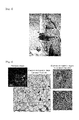
- Fig. 6 shows an example of simultaneous observation of inorganic Q dots as a fluorescent agent by the light microscope 4 and the electron- microscope 2 in the compound microscope device 1.
- Fig. 7 shows an example of simultaneous observation of cultivated cells in which fluorescent protein-fused actin is expressed, by the light microscope 4 and the electron microscope 2 in the compound electron microscope device 1. It is apparent from Figs. 6 and 7 that the electron microscope 2 is higher in resolution power than the light microscope 4. However, in the case of Fig. 6 , search of a field of view for identifying the position of the Q dots can be performed more efficiently by the optical microscope 4. Therefore, the compound microscope device 1 of the present invention, having both the electron microscope 2 and the optical microscopes 4 and 8, allows high-throughput electron microscopic observation.
- a fluorescent portion is identified by the fluorescence microscope ( Fig. 7a ), and then the portion is magnified from lower magnification ( Fig. 7b ) to higher magnifications ( Figs. 7c to 7e ) by the electron microscope, which makes it possible to observe only the region where the fluorescent molecules exist at high resolutions, while avoiding damage to the specimen 10 during search of the field of view.
- actin fibers can be clearly seen in the existence region of fluorescent protein specified by the fluorescence microscope, together with microtubules and ribosome in high-magnification electron microscopic images.
Landscapes
- Chemical & Material Sciences (AREA)
- Analytical Chemistry (AREA)
- Physics & Mathematics (AREA)
- General Physics & Mathematics (AREA)
- Optics & Photonics (AREA)
- Engineering & Computer Science (AREA)
- Multimedia (AREA)
- Computer Vision & Pattern Recognition (AREA)
- Microscoopes, Condenser (AREA)
- Investigating, Analyzing Materials By Fluorescence Or Luminescence (AREA)
Abstract
Description
- The present invention relates to physical and chemical devices using electron rays, in particular, transmission electron microscopes and electron beam analyzers.
- Conventionally, there have been already in practical use devices with a combination of a scanning electron microscope and an optical microscope. For example, Japanese Unexamined Patent Application Publication No.
S53-161215 S55-90046 -
FIGs. 8A and 8B illustrate conventional compound microscope devices. In the device ofFig. 8A , a light microscope is disposed adjacent to an electron microscope main body, and a specimen is horizontally moved between electron optical axes of the light microscope and the electron microscope, whereby the specimen can be observed with switching between the light microscope and the electron microscope. - In addition, there is known a device in which two microscopes are integrated as shown in
Fig. 8B . In this device, a specimen is rotated at 90° to observe light microscopic images of the specimen (J. Struct. Biol. 164 (2008) 183 to 189). -
- [Patent Document 1] Japanese Unexamined Patent Application Publication No.
S55-90046 - [Patent Document 2] Japanese Unexamined Patent Application Publication No.
2010-8406 - [Patent Document 3] Japanese Unexamined Patent Application Publication No.
H5-113418 - [Non-Patent Document 1] Journal of Structural Biology, Volume 164, 2008, pages 183 to 189
- In the techniques disclosed in
Patent Document 1 andNon-Patent Document 1, an optical microscope and a transmission electron microscope can be integrated, but an electron beam and an electron optical axis of light are not aligned with each other, and thus a specimen needs to be observed separately by the light microscope and the electron microscope with movements of the specimen such as translation and rotation. Therefore, it is not possible to observe one specimen simultaneously by the light microscope and the electron microscope even though both imaging functions are integrated into a unit device. - For example, a fluorescence microscope performs a swift operation of searching an area where a fluorescently-stained virus in cells, and an electron microscope performs an operation of fixing (shooting) the searched virus in an enlarged manner. However, it is not possible to search and fix a virus simultaneously on conventional devices. As in the foregoing, conventional devices are not suited for an operation of swiftly detecting a target object and fixing the same, that is, a high-throughput operation.
-
Patent Documents 2 and 3 both disclose devices for observing one specimen with a combination of an electron microscope and a light microscope. However, these techniques are intended for scanning electron microscopes. Accordingly, there has not yet been provided a technique of allowing simultaneous observation of one specimen with a combination of a transmission electron microscope and a light microscope. - Therefore, a major object of the present invention is to provide a device allowing genuinely simultaneous observation of one specimen, with an integration of a transmission electron microscope and a light microscope.
- A compound microscope device of the present invention has a transmission electron microscope and a light microscope as a single entity. The electron microscope has an electron gun that releases an electron ray toward a specimen; an electromagnetic object lens that images the electron ray; and a detection part into which the electron ray having passed through the electromagnetic object lens is entered, wherein a reflection mirror is disposed in a middle of an electronoptical path of the electron ray, and the light microscope includes light object lens in a position separated from the electron-optical path. The reflection mirror has a reflection surface inclined toward the specimen and the light object lens.
The reflection mirror has a mounting center hole penetrating the reflection mirror in a position crossing the movement path. The mounting center hole desirably has a diameter of 0.1 to 1 mm.
It is desired to provide an angle adjustment mechanism for adjusting an inclination angle of the reflection mirror, and it is more desired to provide a lens adjustment mechanism for adjusting the light object lens.
The electromagnetic object lens may include a cylindrical coil and a yoke covering the coil. The yoke may have a portion with a notch, and the portion of the yoke with the notch may be projected toward inside the coil to form a gap within the electromagnetic object lens. The optical object lens and a specimen holder for placement of the specimen, can be arranged in the gap.
The optical microscope may have a light source, a dichroic mirror, and a light detection part. The dichroic mirror, the light object lens, and the light detection part may be arranged in a straight line crossing the electron-optical path. The dichroic mirror desirably has a reflection surface inclined toward the light object lens and the light source. The light object lens may use a fluorescent microscope lens.
The light microscope may include an illumination reflection mirror disposed on the electron-optical path and a light source separated from the electron optical path. The illumination reflection mirror is desirably positioned on an opposite side of the reflection mirror with the specimen therebetween. The illumination reflection mirror desirably has a reflection surface inclined from the electron-optical path toward the specimen and the light source, and a mounting center hole penetrating the illumination reflection mirror in a position crossing the electron-optical path.
It is desired to dispose a light condenser lens on the electron optical path between the illumination reflection mirror and the specimen. The light condenser lens desirably has a mounting center hole penetrating the light condenser lens in a position crossing the electron -optical path.
It is desired to form a transparent conductive material film on one or more of a surface of the reflection mirror; an inner wall surface of the mounting center hole of the reflection mirror; a surface of the illumination reflection mirror; an inner wall surface of the mounting center hole of the illumination reflection mirror; a surface of a lighting reflection mirror; an inner wall surface of a mounting center hole of the lighting reflection mirror; a surface of the optical condenser lens; an inner wall surface of the mounting center hole of the optical condenser lens; and a surface of the optical object lens.
It is desired to dispose the electromagnetic object lens in a vacuum bath and form an anti-reflection film around the light source in an internal space of a vacuum bath. - According to the present invention, it is possible to observe (shoot) simultaneously an electron microscopic image and a light microscopic image of one specimen.
-
-
Fig. 1 is a schematic cross section view of a combination of a compound microscope device of the present invention. -
Fig. 2 is a schematic cross section view of one example of a combination of an electromagnetic object lens and a light object lens. -
Fig. 3 is a schematic cross section view of one example of a combination of an electron magnetic object lens and a light object lens microscope. -
Fig. 4 is a schematic cross section view of another example a combination of an electron magnetic object lens and a light object lens microscope. -
Fig. 5 is a photograph of a specific example of the compound microscope device of the present invention. -
Fig. 6 represents images shot by the compound microscope device of the present invention. -
Fig. 7a is an image shot by a fluorescence microscope, andFig. 7b is an image shot by a low-magnification electron microscope, andFigs. 7c to 7e are images shot by a high-magnification electron microscope. -
Fig. 8A is a schematic diagram of a conventional compound microscope for describing the same, andFig. 8B is a side view of a conventional compound microscope for describing the same. - An embodiment for carrying out the present invention will be described below in detail. However, the present invention is not limited to the embodiment described below.
- In
Fig. 1 ,reference code 1 denotes an example of a compound microscope device of the present invention. Thecompound microscope device 1 has anelectron microscope 2 and anoptical microscope 4. Although there is no particular limitation on structure of theelectron microscope 2, theelectron microscope 2 has avacuum bath 20, anelectron gun 21, aconvergence lens 22, anobject lens 25, aprojection lens 31, and adetection part 30, for example. Thevacuum bath 20 is connected to a vacuum pump not shown to form a vacuum atmosphere within thevacuum bath 20. - The
electron gun 21 has an injection electrode to emit an electron ray (electron beam) directed toward the internal space of thevacuum bath 20, and the electron ray transfers through the interior of thevacuum bath 20 in which the vacuum atmosphere is formed. Reference code C ofFig. 1 denotes an electron-optical path of the electron ray (electron optical axis) injected from theelectron gun 21. Theconvergence lens 22, theobject lens 25, theprojection lens 31, and thedetection part 30 are aligned in this order along the electron- optical axis C from the side closer to theelectron gun 21. The electron ray is converged by theconvergence lens 22, imaged by theobject lens 25, magnified by theprojection lens 31, and then entered into thedetection part 30. - The
electron microscope 2 for use in the present invention is a transmission electron microscope (TEM), and a specimen to be observed is plac at the objective lens, which runs across on the electron-optical axis C. Layout of the specimen and theoptical microscope 4 will be described below together with a specific example of theobject lens 25. -
Fig. 2 is an enlarged cross section view of theobject lens 25. Theobject lens 25 is an electromagnetic lens (magnetic field lens), for example. Hereinafter, theobject lens 25 of theelectron microscope 2 will be referred to aselectromagnetic object lens 25 to differentiate the same from an object lens of thelight microscope 4 described later. Theelectromagnetic object lens 25 has acoil 24 and ayoke 23 covering thecoil 24. Thecoil 24 has a cylindrical shape (ring shape), and theelectromagnetic object lens 25 is also entirely shaped in a cylinder. - The
electromagnetic object lens 25 has an opening at one end of the cylinder directed toward theelectron gun 21 and a central axis line of the cylinder made parallel to the electron -optical axis C of the electron ray. Therefore, the internal space of the cylinder constitutes an electron-optical path 29 of the electron ray. The electron ray is entered from one end (upper end) of the cylinder to the interior of theelectromagnetic object lens 25, and is released downward from the other end (lower end) of the cylinder. - The
yoke 23 has anotch 26. Although there is no particular limitation on shape and position of thenotch 26, thenotch 26 may be formed at the internal side, upper end, or lower end of the cylinder (electromagnetic object lens 25). In each of the cases, thenotch 26 is preferably shaped in a ring surrounding the electron ray. -
Fig. 3 is an enlarged cross section view of a portion shown by reference code A inFig. 2 . The portion of theyoke 23 with thenotch 26 is protruded toward the inner side of the cylinder than thecoil 24, and has a narrowed diameter for theelectron-optical path 29. In the protruded portion (pole piece) of theyoke 23, a differentiation is made between anupper pole 27 closer to theelectron gun 21 and alower pole 28 farther from theelectron gun 21. - In the
yoke 23, at least the portion constituting theupper pole 27 and thelower pole 28 is made of a high magnetic permeability material such as iron cobalt (FeCo). The energizedcoil 24 forms a magnetic line that leaks from theupper pole 27 and thelower pole 28 into the electron-optical path 29, whereby the electron ray is rotated and inflected by the action of a leakage magnetic field. The leakage magnetic field can be controlled to change a position of imaging of the electron ray, by adjusting the shape and/or size of the pole piece, the amount of energization of thecoil 24, and the like. - Since the portion of the
notch 26 is protruded inward, there is formed a gap in the pole piece of theelectromagnetic object lens 25. Aspecimen holder 11 is disposed in the gap. Thespecimen holder 11 has a portion where aspecimen 10 is placed across the electron-optical path 29. The electron ray transferring through the electron-optical path 29 penetrates thespecimen 10 and travels toward thedetection part 30. - When a distance between the
electromagnetic object lens 25 and the specimen 10 (operating distance) becomes longer, a focal distance also becomes longer to thereby increase an aberration. However, it is possible to reduce an aberration and increase a resolution power by placing thespecimen 10 on the inner side of the electromagnetic object lens 25 (electron-optical path 29) as shown inFig. 3 . - A
reflection mirror 41 is disposed on the electron-optical path 29. Thereflection mirror 41 has a penetrating hole (mounting center hole) 42. The mountingcenter hole 42 is positioned on the electron -optical axis C and has a diameter of 0.1 to 1 mm which is larger than a beam diameter of the electron ray. Therefore, the electron ray is not reflected by thereflection mirror 41 but passes through the mountingcenter hole 42. Thereflection mirror 41 may be disposed either on the side nearer thedetection part 30 or theelectron gun 21 than thespecimen 10. The electron ray before or after penetration through thespecimen 10, passes through the mountingcenter hole 42. - The
reflection mirror 41 is positioned between theupper pole 27 and thelower pole 28. Besides thespecimen holder 11, some or all parts of thelight microscope 4 are disposed in the gap of theelectromagnetic object lens 25. Thelight microscope 4 has anobject lens 43, alight source 45, and alight detection part 46. At least theobject lens 43 is disposed in the gap of theelectromagnetic object lens 25 so as to face thereflection mirror 41. Hereinafter, theobject lens 43 of theoptical microscope 4 will be referred to as the light object lens to differentiate the same from theelectromagnetic object lens 25. - The
light source 45 is a mercury lamp, for example. Light emitted from thelight source 45 is made parallel to the electron- optical axis C by anirradiation lens 47. Beyond in the direction of movement of the parallel light path, spectroscopic means is disposed. The spectroscopic means has adichroic mirror 52, for example. Thedichroic mirror 52 has a reflection surface inclined toward theoptical object lens 43 and thelight source 45 at a predetermined angle from a direction parallel to the electron- optical axis C (45° in this embodiment). - Of the parallel light, the light with a predetermined wavelength (excitation light) is bent in the direction of movement toward the
optical object lens 43, and thus moves in a direction crossing the electron optical axis C (orthogonal direction in this embodiment), whereas the light with wavelengths other than that of the excitation light moves straight. Therefore, the excitation light is entered into theoptical object lens 43. It is more desired to dispose anexcitation filter 51 between thedichroic mirror 52 and theirradiation lens 47 to extract the excitation light in advance. - The
dichroic mirror 52, theoptical object lens 43, and thereflection mirror 41 are aligned between theupper pole 27 and thelower pole 28 in a straight line perpendicular to the electron -optical axis C, that is, on a path of the excitation light. The reflection surface of thereflection mirror 41 is inclined at a predetermined angle (45° in this embodiment) from the electron optical- axis C toward thespecimen 10 and thelight object lens 43. After having passed through thelight object lens 43, the excitation light is reflected by thereflection mirror 41 and entered into thespecimen 10. - The
specimen 10 is stained with a fluorescent substance and emits light upon entrance of the excitation light. The fluorescent light is reflected by thereflection mirror 41 and entered into thelight object lens 43. Thelight detection part 46 is disposed on the opposite side of thereflection mirror 41 with thelight object lens 43 there between. Thedichroic mirror 52 resides between thelight object lens 43 and theoptical detection part 46. The fluorescent light is different in wavelength from the excitation light, and thus passes through thedichroic mirror 52 without being reflected. - An
absorption filter 53 and animaging lens 54 may be disposed between thelight detection part 46 and thedichroic mirror 52. In this case, the fluorescent light is cleared by theabsorption filter 53 of the excitation light and scattered light, imaged at theimaging lens 54, and then entered into thelight detection part 46. Thelight detection part 46 is a CCD camera or the like, for example. Thelight detection part 46 is connected to a processing device in a computer or the like to perform an arithmetical process on the fluorescent light captured at thelight detection part 46, and output results of the process to an output device (image display, printing, or the like). As in the foregoing, thelight microscope 4 shown inFig. 3 is a so-called incident-light fluorescence microscope that is capable of separating the excitation light and the fluorescent light by thedichroic mirror 52, and observing and/or shooting thespecimen 10. - The electron ray to pass through the
electromagnetic object lens 25 has a small beam diameter, and thus can pass through the mountingcenter hole 42 even if the diameter of the mountingcenter hole 42 is made as small as about 0.1 to 1.0 mm such that sufficient amounts of excitation light and fluorescent light can be reflected by thereflection mirror 41. Therefore, thecompound microscope device 1 allows electron ray irradiation and light irradiation to thespecimen 10 in a coaxial manner. This allows observation and shooting of thespecimen 10, simultaneously by thetransmission electron microscope 2 and theoptical microscope 4. - The
light microscope 4 for use in the present invention is not limited to a fluorescence microscope. Another example of an optical microscope will be described below. InFig. 4 ,reference code 8 denotes a bright-field light microscope. This microscope will be described with the same reference codes as those shown inFig. 3 given to the same members as those shown inFig. 3 . In thelight microscope 8, theoptical detection part 46 and thelight object lens 43 may be structured and arranged in the same manner as those in thelight microscope 4 shown inFig. 3 , except for location of alight source 85. - The
light source 85 is disposed above theupper pole 27, for example. Thelight source 85 is directed toward the electron optical axis C. Anillumination reflection mirror 81 is disposed on the electron optical axis C in a position opposed to thelight source 85. Thespecimen 10 can be disposed on the electron-optical path 29 inside theelectromagnetic object lens 25 as in the case ofFig. 3 . Theillumination reflection mirror 81 has a reflection surface inclined at a predetermined angle (45° in this embodiment) from the electron -optical axis C toward thespecimen 10 and thelight source 85. - An
irradiation lens 87 is disposed between thelight source 85 and theillumination reflection mirror 81, and light from thelight source 85 is collected by theirradiation lens 87 onto the reflection surface of theillumination reflection mirror 81 and reflected by the reflection surface toward thespecimen 10. - The
illumination reflection mirror 81 is separated from theupper pole 27 and thus there is a long distance from theillumination reflection mirror 81 to thespecimen 10. In this case, a light condenser lens (light-collecting lens) 83 is interposed between theillumination reflection mirror 81 and thespecimen 10. In this embodiment, thelight condenser lens 83 is attached to theupper pole 27, and thus light is collected by thelight condenser lens 83 and then entered into thespecimen 10. - A
light reflection mirror 88 is disposed on the opposite side of theillumination reflection mirror 81 with thespecimen 10 therebetween. Thelighting reflection mirror 88 has a reflection surface inclined at a predetermined angle (45° in this embodiment) from the electron -optical axis C toward thespecimen 10 and theoptical object lens 43, as with thereflection mirror 41 shown inFig. 3 . Therefore, light having been transmitted through thespecimen 10 is reflected by thelighting reflection mirror 88 and entered into thelight object lens 43. Beyond in a direction of the transmitted light, thelight detection part 46 is disposed as in the first example (Fig. 3 ). Therefore, the transmitted light is entered into thelight detection part 46 directly or after passing through theabsorption filter 53 and theimaging lens 54. - The
illumination reflection mirror 81, thelight condenser lens 83, and thelight reflection mirror 88 are aligned on the electron- optical axis C of the electron ray, and have respective penetrating holes (mounting center holes) 82, 84, and 89 at positions thereof falling on the electron-optical path. As with thereflection mirror 41 shown inFig. 3 , the mounting center holes 82, 84, and 89 each have a diameter set so as not to prevent passage of the electron ray (0.1 to 1 mm). Therefore, thelight microscope 8 ofFig. 4 allows observation and shooting of thespecimen 10, simultaneously by thetransmission electron microscope 2 and thelight microscope 8. - The
light source 85 and theillumination reflection mirror 81 may be disposed under the lower pole 28 (that is, thedetection part 30 side). In this case, thelight reflection mirror 88 is disposed nearer theupper pole 27 than thespecimen 10 to let in light having transmitted through thespecimen 10 from underneath. - In the device of
Fig. 4 , spectroscopic means (a dichroic mirror, an excitation filter, or the like) is disposed between thelight source 85 and theillumination reflection mirror 81 to extract the excitation light, whereby the spectroscopic means can be used as a fluorescence microscope. In this case, the fluorescence microscope detects fluorescent light released from thespecimen 10 toward thelighting reflection mirror 88. - There is no particular limitation on the
light object lens 43 for use in the present invention, and thelight object lens 43 can use a lens equivalent to a commercially available object lens with a long working distance. It is desired to use theoptical object lens 43 having a working distance at which the reflection mirrors 41 and 88 can be disposed between thespecimen 10 and theoptical object lens 43. - Since the
light object lens 43 is placed in a ferromagnetic field and a vacuum, thelight object lens 43 needs to be non-magnetic and have vacuum-resistance performance. Specifically, it is desired to change a material for a lens case body for holding thelight object lens 43 from brass to non-magnetic material (for example, phosphor bronze), and form a small hole in the lens case body so as to allow communication between the space in the glass lens and a surrounding vacuum part. - In addition, although there is no particular limitation on the
convergence lens 22 and theprojection lens 31 of theelectron microscope 2, a magnetic lens having a structure similar to that of theelectromagnetic object lens 25 may be used, for example. It is desired to apply conductive coating to surfaces of the reflection mirrors 41, 81, and 88 and/or inner wall surfaces of the mounting center holes 42, 82, and 89, a surface of thelight condenser lens 83 and/or an inner wall surface of the mountingcenter hole 84, and a surface of thelight object lens 43, for prevention of electrostatic charge by the electron ray. As a material for the conductive coating, a material with a high light transmittance, for example, one or more kinds of transparent conductive materials selected from the group consisting of indium tin oxide (ITO), zinc oxide (IZO), and indium-gallium-zinc oxide (IGZO). - The
compound microscope device 1 of the present invention emits light for light observation into the electron-optical path of the electron ray. Therefore, it is desired to apply an anti-reflection treatment (anti-reflection film) to surfaces of members of theelectron microscope 2 in positions to which light (excitation light, fluorescent light, reflected light, and the like) is emitted, that is, surfaces of members around thespecimen 10. - The anti-reflection treatment is a blackening treatment, for example. It is effective from a viewpoint of anti-reflection to apply the blackening treatment to the
specimen holder 10, the pole piece portion of theelectromagnetic object lens 25, a cooling fan for prevention of specimen contamination in theelectron microscope 2, a leading end of a diaphragm unit of the electron microscope 25 (in particular, for the electromagnetic object lens 25), a portion for setting a diaphragm of theelectromagnetic object lens 25, a wall surface of thevacuum bath 20 around theelectromagnetic object lens 25, and the like, for example. There is no particular limitation on material for use in the blackening treatment as far as the material is a low-reflection, non-magnetic material, and thus various kinds of materials such as titanium black can be used. - It is desired to connect the reflection mirrors 41, 81, and 88 to an
angle adjustment mechanism 91 such that inclination angles of the reflection mirrors 41, 81, and 88 can be changed by operations from outside of thevacuum bath 20. In this case, the angles of the reflection mirrors 41, 81, and 88 can be finely adjusted in accordance with the kind and position of thespecimen 10, the kind of a fluorescent substance, excitation light, and the like, thereby allowing observation and shooting of thespecimen 10 in various manners. - In addition, it is desired to connect a
lens adjustment mechanism 92 to thelight object lens 43 such that distances from thelight object lens 43 to the reflection mirrors 41 and 88 or the like can be changed by operations from outside of thevacuum bath 20. In this case, the focus of thelight object lens 43 can be finely adjusted in accordance with the kind of thespecimen 10 and the like, thereby allowing observation and shooting of thespecimen 10 in various manners. - Next, an example of use of the
compound microscope device 1 of the present invention will be described.
In the case of observing a biological specimen with a specific organ or cell fluorescently stained, for prevention of damage to thespecimen 10 due to the electron ray, first no electron ray is emitted to thespecimen 10 but a field of view is searched only by theoptical microscopes specimen 10 is fluorescently stained, it is possible to search a field of view more efficiently as compared to the case of using theelectron microscope 2. - In the course of search of the field of view, the electron ray is displaced from the
specimen 10 by a deflection coil. When any subject to be observed at high resolution is discovered, the electron ray is returned to thespecimen 10 for high-resolution observation by theelectron microscope 2. The deflection coil is disposed between theconvergence lens 22 and theelectromagnetic object lens 25, for example. As in the foregoing, it is important to set a time for irradiating the electron ray to the specimen as short as possible for reductionof damage to thespecimen 10. -
Fig. 5 is a photograph of an outer appearance of one example of thecompound microscope device 1 of the present invention. In an encircled portion of the photograph, thelight microscopes electromagnetic object lens 25.Fig. 6 shows an example of simultaneous observation of inorganic Q dots as a fluorescent agent by thelight microscope 4 and the electron-microscope 2 in thecompound microscope device 1. -
Fig. 7 shows an example of simultaneous observation of cultivated cells in which fluorescent protein-fused actin is expressed, by thelight microscope 4 and theelectron microscope 2 in the compoundelectron microscope device 1. It is apparent fromFigs. 6 and7 that theelectron microscope 2 is higher in resolution power than thelight microscope 4. However, in the case ofFig. 6 , search of a field of view for identifying the position of the Q dots can be performed more efficiently by theoptical microscope 4. Therefore, thecompound microscope device 1 of the present invention, having both theelectron microscope 2 and theoptical microscopes - When a biological specimen is observed by a conventional electron microscope, the biological specimen may be damaged by the electron ray during search of a field of view. According to the
compound microscope device 1 of the present invention however, first, a fluorescent portion is identified by the fluorescence microscope (Fig. 7a ), and then the portion is magnified from lower magnification (Fig. 7b ) to higher magnifications (Figs. 7c to 7e ) by the electron microscope, which makes it possible to observe only the region where the fluorescent molecules exist at high resolutions, while avoiding damage to thespecimen 10 during search of the field of view. In actuality, in the case ofFig. 7 , actin fibers can be clearly seen in the existence region of fluorescent protein specified by the fluorescence microscope, together with microtubules and ribosome in high-magnification electron microscopic images. - In addition, by combination of an already actually utilized atmospheric specimen chamber for electron microscopes and phase-contrast electron microscopy, it is possible to observe a biological specimen in the living state by optical microscopy while observing the specimen at high resolution and with high contrast for specific moments by the phase-contrast electron microscopy, in the same field of view. This allows functionality and structure of the biological body to be observed and associated with each other in real time.
-
- 1:
- Compound microscope device
- 2:
- Electron microscope
- 4, 8:
- Light microscope
- 10:
- Specimen
- 11:
- Specimen holder
- 20:
- Vacuum chamber
- 21:
- Electron gun
- 23:
- Yoke
- 24:
- Coil
- 25:
- Electromagnetic object lens
- 30:
- Detection part
- 41, 81, 88:
- Reflection mirror
- 42, 82, 89:
- Mounting center hole (penetrating hole)
- 43:
- Light object lens
- 45:
- Light source
- 46:
- Light detection part
- 52:
- Dichroic mirror
- 83:
- Light condenser lens
- 91:
- Angle adjustment mechanism
- 92:
- Lens adjustment mechanism
- C:
- Electron- optical axis (movement path)
Claims (11)
- A compound microscope device comprising a transmission electron microscope and a light microscope, wherein
the electron microscope has an electron gun that releases an electron ray toward a specimen; an electromagnetic object lens that images the electron ray; and a detection part into which the electron ray having passed through the electromagnetic object lens is entered,
a reflection mirror is disposed in a middle of an electron-optical path,
the optical microscope includes a light object lens disposed in a position separated from the electron-optical path,
the reflection mirror has a reflection surface inclined toward the specimen and the optical object lens, and
the reflection mirror has a mounting center hole penetrating the reflection mirror in a position crossing the movement path. - The compound microscope device according to Claim 1, wherein the mounting center hole has a diameter of 0.1 to 1 mm.
- The compound microscope device according to Claim 1 or 2, comprising an angle adjustment mechanism for adjusting an inclination angle of the reflection mirror.
- The compound microscope device according to any one of Claims 1 to 3, comprising a lens adjustment mechanism for adjusting the optical object lens.
- The compound microscope device according to any one of Claims 1 to 4, wherein
the electromagnetic object lens has a cylindrical coil and a yoke covering the coil,
the yoke has a portion with a notch,
the portion of the yoke with the notch is projected toward inside the coil to form a gap within the electromagnetic object lens, and
the light object lens and a specimen holder for placement of the specimen, are arranged in the gap. - The compound microscope device according to any one of Claims 1 to 5, wherein
the light microscope has a light source, a dichroic mirror, and an optical detection part,
the dichroic mirror, the light object lens, and the light detection part are arranged in a straight line crossing the electron-optical path, and
the reflection mirror has a reflection surface inclined toward the light object lens and the light source. - The compound microscope device according to Claim 6, wherein the light object lens is a fluorescent microscope lens.
- The compound microscope device according to any one of Claims 1 to 5, wherein
the optical microscope has an illumination reflection mirror disposed on the movement path and a light source separated from the movement path,
the illumination reflection mirror is positioned on an opposite side of the reflection mirror with the specimen therebetween,
the illumination reflection mirror has a reflection surface inclined from the movement path toward the specimen and the light source, and
the illumination reflection mirror has a mounting center hole penetrating the illumination reflection mirror in a position crossing the movement path. - The compound microscope device according to Claim 8, wherein
an optical condenser lens is disposed on the movement path between the illumination reflection mirror and the specimen, and
the optical condenser lens has a mounting center hole penetrating the optical condenser lens in a position crossing the movement path. - The compound microscope device according to Claim 9, wherein a transparent conductive material film is formed on one or more of a surface of the reflection mirror; an inner wall surface of the mounting center hole of the reflection mirror; a surface of the illumination reflection mirror; an inner wall surface of the mounting center hole of the illumination reflection mirror; a surface of the lighting reflection mirror; an inner wall surface of a mounting center hole of the lighting reflection mirror; a surface of the optical condenser lens; an inner wall surface of the mounting center hole of the optical condenser lens; and a surface of the optical object lens.
- The compound microscope device according to any one of Claims 1 to 10, wherein
the electromagnetic object lens is disposed in a vacuum bath, and
an anti-reflection film is formed around the light source in an internal space of a vacuum bath.
Applications Claiming Priority (2)
| Application Number | Priority Date | Filing Date | Title |
|---|---|---|---|
| JP2010088201 | 2010-04-06 | ||
| PCT/JP2011/058684 WO2011126041A1 (en) | 2010-04-06 | 2011-04-06 | Compound microscope device |
Publications (3)
| Publication Number | Publication Date |
|---|---|
| EP2557588A1 true EP2557588A1 (en) | 2013-02-13 |
| EP2557588A4 EP2557588A4 (en) | 2014-01-15 |
| EP2557588B1 EP2557588B1 (en) | 2017-07-12 |
Family
ID=44762975
Family Applications (1)
| Application Number | Title | Priority Date | Filing Date |
|---|---|---|---|
| EP11765941.7A Not-in-force EP2557588B1 (en) | 2010-04-06 | 2011-04-06 | Combined charged particle beam and fluorescence microscope |
Country Status (4)
| Country | Link |
|---|---|
| US (1) | US9310596B2 (en) |
| EP (1) | EP2557588B1 (en) |
| JP (1) | JP5842308B2 (en) |
| WO (1) | WO2011126041A1 (en) |
Families Citing this family (9)
| Publication number | Priority date | Publication date | Assignee | Title |
|---|---|---|---|---|
| EP2899743B1 (en) * | 2014-01-27 | 2016-09-21 | Fei Company | Correlative optical and charged particle microscope |
| CN104091745B (en) * | 2014-07-18 | 2016-06-01 | 镇江乐华电子科技有限公司 | An integrated structure integrating TEM fluorescent screen and STEM detector |
| KR101693539B1 (en) * | 2015-11-12 | 2017-01-06 | 한국표준과학연구원 | High resolution correlative light and electron microscope |
| EP3385977B1 (en) * | 2015-12-03 | 2021-07-28 | Matsusada Precision, Inc. | Charged particle beam device and scanning electron microscope |
| KR101727196B1 (en) * | 2015-12-18 | 2017-04-14 | 한국표준과학연구원 | Infrared-electron correlative microscope |
| GB201704275D0 (en) | 2017-03-17 | 2017-05-03 | Science And Tech Facilities Council | Super-resolution microscopy |
| JP7159011B2 (en) * | 2018-11-08 | 2022-10-24 | 株式会社日立ハイテク | Electron beam device |
| KR102168726B1 (en) * | 2019-04-23 | 2020-10-22 | 한국표준과학연구원 | An Optical Objective Lens Alignment Mount for Sample Chamber, Light Reflection Mirror Having Electron Through-hole Attached on The Mount, and Correlative Light and Electron Microscope with Spectroscopy including the Same |
| CN114324436A (en) * | 2021-12-23 | 2022-04-12 | 江苏大学 | A laser processing and real-time in-situ high-resolution observation device for micro-nano structures |
Family Cites Families (22)
| Publication number | Priority date | Publication date | Assignee | Title |
|---|---|---|---|---|
| US2233286A (en) * | 1939-01-27 | 1941-02-25 | Rca Corp | Electronic and light microscope |
| DE1099659B (en) * | 1958-08-30 | 1961-02-16 | Zeiss Carl Fa | Shielding device |
| JPS53161215U (en) | 1977-05-26 | 1978-12-16 | ||
| JPS5532304A (en) | 1978-08-28 | 1980-03-07 | Internatl Precision Inc | Electron microscope with optical microscope |
| JPS5590046A (en) | 1978-12-28 | 1980-07-08 | Internatl Precision Inc | Electronic microscope equipped with optical microscope provided with x-ray shielding device |
| JPS56121151U (en) * | 1980-02-15 | 1981-09-16 | ||
| GB2130433B (en) * | 1982-03-05 | 1986-02-05 | Jeol Ltd | Scanning electron microscope with as optical microscope |
| FR2596863B1 (en) * | 1986-04-07 | 1988-06-17 | Centre Nat Rech Scient | ANALYTICAL MICROSCOPY DEVICE CAPABLE OF FORMING BOTH A RAMAN PROBE AND AN ELECTRONIC PROBE |
| JPH0614458B2 (en) | 1987-05-28 | 1994-02-23 | 日本電子株式会社 | Magnetic domain observation device |
| JP2578519B2 (en) * | 1990-06-01 | 1997-02-05 | 株式会社日立製作所 | Charged particle beam exposure system with position detection function by light beam |
| JP3003708B2 (en) | 1990-12-25 | 2000-01-31 | 株式会社島津製作所 | Surface analyzer |
| JP3040663B2 (en) * | 1994-07-15 | 2000-05-15 | 財団法人ファインセラミックスセンター | Heating device for electron microscope |
| JPH11250850A (en) * | 1998-03-02 | 1999-09-17 | Hitachi Ltd | Scanning electron microscope, microscope method, and interactive input device |
| EP0995086B1 (en) | 1998-05-09 | 2007-11-14 | Renishaw plc | Electron microscope and spectroscopy system |
| US6885445B2 (en) | 1998-05-09 | 2005-04-26 | Renishaw Plc | Electron microscope and spectroscopy system |
| US6859313B2 (en) | 2001-03-23 | 2005-02-22 | Japan Science & Technology Corporation | Super resolution microscope |
| JP2003066338A (en) | 2001-08-28 | 2003-03-05 | Olympus Optical Co Ltd | microscope |
| JP2007292702A (en) * | 2006-04-27 | 2007-11-08 | Jeol Ltd | Sample inspection apparatus, sample inspection method, and sample inspection system |
| JP2007322396A (en) | 2006-06-05 | 2007-12-13 | Univ Of Tsukuba | Combined microscope of transmission electron microscope and near-field optical microscope |
| EP1953791A1 (en) | 2007-02-05 | 2008-08-06 | FEI Company | Apparatus for observing a sample with a particle beam and an optical microscope |
| JP2010008406A (en) | 2008-05-30 | 2010-01-14 | Shinichiro Isobe | Multiple light source microscope |
| DE102010011898A1 (en) * | 2010-03-18 | 2011-09-22 | Carl Zeiss Nts Gmbh | inspection system |
-
2011
- 2011-04-06 EP EP11765941.7A patent/EP2557588B1/en not_active Not-in-force
- 2011-04-06 US US13/638,981 patent/US9310596B2/en not_active Expired - Fee Related
- 2011-04-06 JP JP2012509683A patent/JP5842308B2/en not_active Expired - Fee Related
- 2011-04-06 WO PCT/JP2011/058684 patent/WO2011126041A1/en not_active Ceased
Also Published As
| Publication number | Publication date |
|---|---|
| EP2557588A4 (en) | 2014-01-15 |
| JP5842308B2 (en) | 2016-01-13 |
| JPWO2011126041A1 (en) | 2013-07-11 |
| WO2011126041A1 (en) | 2011-10-13 |
| US9310596B2 (en) | 2016-04-12 |
| EP2557588B1 (en) | 2017-07-12 |
| US20130088775A1 (en) | 2013-04-11 |
Similar Documents
| Publication | Publication Date | Title |
|---|---|---|
| EP2557588B1 (en) | Combined charged particle beam and fluorescence microscope | |
| Kuba et al. | Advanced cryo‐tomography workflow developments–correlative microscopy, milling automation and cryo‐lift‐out | |
| Zonnevylle et al. | Integration of a high‐NA light microscope in a scanning electron microscope | |
| CN101241087B (en) | Apparatus for observing a sample with a particle beam and an optical microscope | |
| US8472113B2 (en) | Scanning microscope and method for light-microscopic imaging of an object | |
| CN107526156B (en) | Light sheet microscope and method for operating a light sheet microscope | |
| Kaech | Introduction to Electron Microscopy | |
| JP6400283B2 (en) | Configurable charged particle device | |
| US9293297B2 (en) | Correlative optical and charged particle microscope | |
| CN115997113B (en) | Method and apparatus for micromachining of samples using a focused ion beam | |
| JP2010008406A (en) | Multiple light source microscope | |
| JP2015141899A5 (en) | ||
| EP1724809A1 (en) | Particle-optical apparatus for the irradiation of a sample | |
| US20130044370A1 (en) | Device and method for scanning an object and a microscope | |
| CN119731762A (en) | Device for multimodal analysis of sample material | |
| US9966223B2 (en) | Device for correlative scanning transmission electron microscopy (STEM) and light microscopy | |
| Mualla et al. | Microscopy | |
| US20250029806A1 (en) | Transmission electron microscopy with square beams | |
| CN113707521B (en) | Axial alignment assembly and charged particle microscope comprising such an alignment assembly | |
| JP2024088618A (en) | Pole piece incorporating optical cavity for improved phase-contrast in electron microscope imaging | |
| KR101693539B1 (en) | High resolution correlative light and electron microscope | |
| CN115061270B (en) | Inclination mode telescopic microscopic combined imaging method | |
| Basha | Microscopy and Specimen Preparation | |
| Haloi | Light and Electron Microscope | |
| CN115128788A (en) | Horizontal placement of the microscope unit parallel to the object under observation |
Legal Events
| Date | Code | Title | Description |
|---|---|---|---|
| PUAI | Public reference made under article 153(3) epc to a published international application that has entered the european phase |
Free format text: ORIGINAL CODE: 0009012 |
|
| 17P | Request for examination filed |
Effective date: 20121102 |
|
| AK | Designated contracting states |
Kind code of ref document: A1 Designated state(s): AL AT BE BG CH CY CZ DE DK EE ES FI FR GB GR HR HU IE IS IT LI LT LU LV MC MK MT NL NO PL PT RO RS SE SI SK SM TR |
|
| DAX | Request for extension of the european patent (deleted) | ||
| A4 | Supplementary search report drawn up and despatched |
Effective date: 20131218 |
|
| RIC1 | Information provided on ipc code assigned before grant |
Ipc: H01J 37/22 20060101ALI20131212BHEP Ipc: H01J 37/26 20060101AFI20131212BHEP Ipc: H01J 37/16 20060101ALI20131212BHEP Ipc: H01J 37/20 20060101ALI20131212BHEP Ipc: H01J 37/141 20060101ALI20131212BHEP |
|
| RAP1 | Party data changed (applicant data changed or rights of an application transferred) |
Owner name: JEOL LTD. Owner name: NAGAYAMA, KUNIAKI Owner name: INTER-UNIVERSITY RESEARCH INSTITUTE CORPORATION NA |
|
| GRAP | Despatch of communication of intention to grant a patent |
Free format text: ORIGINAL CODE: EPIDOSNIGR1 |
|
| INTG | Intention to grant announced |
Effective date: 20170208 |
|
| RIN1 | Information on inventor provided before grant (corrected) |
Inventor name: TERAKAWA, SUSUMU Inventor name: IIJIMA, HIROFUMI Inventor name: ARAI, YOSHIHIRO Inventor name: NAGAYAMA, KUNIAKI |
|
| GRAS | Grant fee paid |
Free format text: ORIGINAL CODE: EPIDOSNIGR3 |
|
| GRAA | (expected) grant |
Free format text: ORIGINAL CODE: 0009210 |
|
| RAP1 | Party data changed (applicant data changed or rights of an application transferred) |
Owner name: JEOL LTD. |
|
| AK | Designated contracting states |
Kind code of ref document: B1 Designated state(s): AL AT BE BG CH CY CZ DE DK EE ES FI FR GB GR HR HU IE IS IT LI LT LU LV MC MK MT NL NO PL PT RO RS SE SI SK SM TR |
|
| REG | Reference to a national code |
Ref country code: GB Ref legal event code: FG4D |
|
| REG | Reference to a national code |
Ref country code: CH Ref legal event code: EP |
|
| REG | Reference to a national code |
Ref country code: AT Ref legal event code: REF Ref document number: 909083 Country of ref document: AT Kind code of ref document: T Effective date: 20170715 |
|
| REG | Reference to a national code |
Ref country code: IE Ref legal event code: FG4D |
|
| REG | Reference to a national code |
Ref country code: NL Ref legal event code: FP |
|
| REG | Reference to a national code |
Ref country code: DE Ref legal event code: R096 Ref document number: 602011039523 Country of ref document: DE |
|
| REG | Reference to a national code |
Ref country code: LT Ref legal event code: MG4D |
|
| REG | Reference to a national code |
Ref country code: AT Ref legal event code: MK05 Ref document number: 909083 Country of ref document: AT Kind code of ref document: T Effective date: 20170712 |
|
| PG25 | Lapsed in a contracting state [announced via postgrant information from national office to epo] |
Ref country code: AT Free format text: LAPSE BECAUSE OF FAILURE TO SUBMIT A TRANSLATION OF THE DESCRIPTION OR TO PAY THE FEE WITHIN THE PRESCRIBED TIME-LIMIT Effective date: 20170712 Ref country code: HR Free format text: LAPSE BECAUSE OF FAILURE TO SUBMIT A TRANSLATION OF THE DESCRIPTION OR TO PAY THE FEE WITHIN THE PRESCRIBED TIME-LIMIT Effective date: 20170712 Ref country code: SE Free format text: LAPSE BECAUSE OF FAILURE TO SUBMIT A TRANSLATION OF THE DESCRIPTION OR TO PAY THE FEE WITHIN THE PRESCRIBED TIME-LIMIT Effective date: 20170712 Ref country code: LT Free format text: LAPSE BECAUSE OF FAILURE TO SUBMIT A TRANSLATION OF THE DESCRIPTION OR TO PAY THE FEE WITHIN THE PRESCRIBED TIME-LIMIT Effective date: 20170712 Ref country code: NO Free format text: LAPSE BECAUSE OF FAILURE TO SUBMIT A TRANSLATION OF THE DESCRIPTION OR TO PAY THE FEE WITHIN THE PRESCRIBED TIME-LIMIT Effective date: 20171012 Ref country code: FI Free format text: LAPSE BECAUSE OF FAILURE TO SUBMIT A TRANSLATION OF THE DESCRIPTION OR TO PAY THE FEE WITHIN THE PRESCRIBED TIME-LIMIT Effective date: 20170712 |
|
| PG25 | Lapsed in a contracting state [announced via postgrant information from national office to epo] |
Ref country code: ES Free format text: LAPSE BECAUSE OF FAILURE TO SUBMIT A TRANSLATION OF THE DESCRIPTION OR TO PAY THE FEE WITHIN THE PRESCRIBED TIME-LIMIT Effective date: 20170712 Ref country code: BG Free format text: LAPSE BECAUSE OF FAILURE TO SUBMIT A TRANSLATION OF THE DESCRIPTION OR TO PAY THE FEE WITHIN THE PRESCRIBED TIME-LIMIT Effective date: 20171012 Ref country code: PL Free format text: LAPSE BECAUSE OF FAILURE TO SUBMIT A TRANSLATION OF THE DESCRIPTION OR TO PAY THE FEE WITHIN THE PRESCRIBED TIME-LIMIT Effective date: 20170712 Ref country code: IS Free format text: LAPSE BECAUSE OF FAILURE TO SUBMIT A TRANSLATION OF THE DESCRIPTION OR TO PAY THE FEE WITHIN THE PRESCRIBED TIME-LIMIT Effective date: 20171112 Ref country code: GR Free format text: LAPSE BECAUSE OF FAILURE TO SUBMIT A TRANSLATION OF THE DESCRIPTION OR TO PAY THE FEE WITHIN THE PRESCRIBED TIME-LIMIT Effective date: 20171013 Ref country code: RS Free format text: LAPSE BECAUSE OF FAILURE TO SUBMIT A TRANSLATION OF THE DESCRIPTION OR TO PAY THE FEE WITHIN THE PRESCRIBED TIME-LIMIT Effective date: 20170712 Ref country code: LV Free format text: LAPSE BECAUSE OF FAILURE TO SUBMIT A TRANSLATION OF THE DESCRIPTION OR TO PAY THE FEE WITHIN THE PRESCRIBED TIME-LIMIT Effective date: 20170712 |
|
| REG | Reference to a national code |
Ref country code: DE Ref legal event code: R097 Ref document number: 602011039523 Country of ref document: DE |
|
| PG25 | Lapsed in a contracting state [announced via postgrant information from national office to epo] |
Ref country code: CZ Free format text: LAPSE BECAUSE OF FAILURE TO SUBMIT A TRANSLATION OF THE DESCRIPTION OR TO PAY THE FEE WITHIN THE PRESCRIBED TIME-LIMIT Effective date: 20170712 Ref country code: RO Free format text: LAPSE BECAUSE OF FAILURE TO SUBMIT A TRANSLATION OF THE DESCRIPTION OR TO PAY THE FEE WITHIN THE PRESCRIBED TIME-LIMIT Effective date: 20170712 Ref country code: DK Free format text: LAPSE BECAUSE OF FAILURE TO SUBMIT A TRANSLATION OF THE DESCRIPTION OR TO PAY THE FEE WITHIN THE PRESCRIBED TIME-LIMIT Effective date: 20170712 |
|
| PLBE | No opposition filed within time limit |
Free format text: ORIGINAL CODE: 0009261 |
|
| STAA | Information on the status of an ep patent application or granted ep patent |
Free format text: STATUS: NO OPPOSITION FILED WITHIN TIME LIMIT |
|
| PG25 | Lapsed in a contracting state [announced via postgrant information from national office to epo] |
Ref country code: EE Free format text: LAPSE BECAUSE OF FAILURE TO SUBMIT A TRANSLATION OF THE DESCRIPTION OR TO PAY THE FEE WITHIN THE PRESCRIBED TIME-LIMIT Effective date: 20170712 Ref country code: SK Free format text: LAPSE BECAUSE OF FAILURE TO SUBMIT A TRANSLATION OF THE DESCRIPTION OR TO PAY THE FEE WITHIN THE PRESCRIBED TIME-LIMIT Effective date: 20170712 Ref country code: SM Free format text: LAPSE BECAUSE OF FAILURE TO SUBMIT A TRANSLATION OF THE DESCRIPTION OR TO PAY THE FEE WITHIN THE PRESCRIBED TIME-LIMIT Effective date: 20170712 Ref country code: IT Free format text: LAPSE BECAUSE OF FAILURE TO SUBMIT A TRANSLATION OF THE DESCRIPTION OR TO PAY THE FEE WITHIN THE PRESCRIBED TIME-LIMIT Effective date: 20170712 |
|
| 26N | No opposition filed |
Effective date: 20180413 |
|
| PG25 | Lapsed in a contracting state [announced via postgrant information from national office to epo] |
Ref country code: SI Free format text: LAPSE BECAUSE OF FAILURE TO SUBMIT A TRANSLATION OF THE DESCRIPTION OR TO PAY THE FEE WITHIN THE PRESCRIBED TIME-LIMIT Effective date: 20170712 |
|
| PG25 | Lapsed in a contracting state [announced via postgrant information from national office to epo] |
Ref country code: MC Free format text: LAPSE BECAUSE OF FAILURE TO SUBMIT A TRANSLATION OF THE DESCRIPTION OR TO PAY THE FEE WITHIN THE PRESCRIBED TIME-LIMIT Effective date: 20170712 |
|
| REG | Reference to a national code |
Ref country code: CH Ref legal event code: PL |
|
| REG | Reference to a national code |
Ref country code: BE Ref legal event code: MM Effective date: 20180430 |
|
| REG | Reference to a national code |
Ref country code: IE Ref legal event code: MM4A |
|
| PG25 | Lapsed in a contracting state [announced via postgrant information from national office to epo] |
Ref country code: LU Free format text: LAPSE BECAUSE OF NON-PAYMENT OF DUE FEES Effective date: 20180406 |
|
| PG25 | Lapsed in a contracting state [announced via postgrant information from national office to epo] |
Ref country code: BE Free format text: LAPSE BECAUSE OF NON-PAYMENT OF DUE FEES Effective date: 20180430 Ref country code: LI Free format text: LAPSE BECAUSE OF NON-PAYMENT OF DUE FEES Effective date: 20180430 Ref country code: CH Free format text: LAPSE BECAUSE OF NON-PAYMENT OF DUE FEES Effective date: 20180430 |
|
| PG25 | Lapsed in a contracting state [announced via postgrant information from national office to epo] |
Ref country code: FR Free format text: LAPSE BECAUSE OF NON-PAYMENT OF DUE FEES Effective date: 20180430 Ref country code: IE Free format text: LAPSE BECAUSE OF NON-PAYMENT OF DUE FEES Effective date: 20180406 |
|
| PGFP | Annual fee paid to national office [announced via postgrant information from national office to epo] |
Ref country code: NL Payment date: 20190418 Year of fee payment: 9 |
|
| PGFP | Annual fee paid to national office [announced via postgrant information from national office to epo] |
Ref country code: DE Payment date: 20190418 Year of fee payment: 9 |
|
| PGFP | Annual fee paid to national office [announced via postgrant information from national office to epo] |
Ref country code: GB Payment date: 20190418 Year of fee payment: 9 |
|
| PG25 | Lapsed in a contracting state [announced via postgrant information from national office to epo] |
Ref country code: MT Free format text: LAPSE BECAUSE OF NON-PAYMENT OF DUE FEES Effective date: 20180406 |
|
| PG25 | Lapsed in a contracting state [announced via postgrant information from national office to epo] |
Ref country code: TR Free format text: LAPSE BECAUSE OF FAILURE TO SUBMIT A TRANSLATION OF THE DESCRIPTION OR TO PAY THE FEE WITHIN THE PRESCRIBED TIME-LIMIT Effective date: 20170712 |
|
| PG25 | Lapsed in a contracting state [announced via postgrant information from national office to epo] |
Ref country code: HU Free format text: LAPSE BECAUSE OF FAILURE TO SUBMIT A TRANSLATION OF THE DESCRIPTION OR TO PAY THE FEE WITHIN THE PRESCRIBED TIME-LIMIT; INVALID AB INITIO Effective date: 20110406 Ref country code: PT Free format text: LAPSE BECAUSE OF FAILURE TO SUBMIT A TRANSLATION OF THE DESCRIPTION OR TO PAY THE FEE WITHIN THE PRESCRIBED TIME-LIMIT Effective date: 20170712 |
|
| PG25 | Lapsed in a contracting state [announced via postgrant information from national office to epo] |
Ref country code: CY Free format text: LAPSE BECAUSE OF FAILURE TO SUBMIT A TRANSLATION OF THE DESCRIPTION OR TO PAY THE FEE WITHIN THE PRESCRIBED TIME-LIMIT Effective date: 20170712 Ref country code: MK Free format text: LAPSE BECAUSE OF NON-PAYMENT OF DUE FEES Effective date: 20170712 |
|
| PG25 | Lapsed in a contracting state [announced via postgrant information from national office to epo] |
Ref country code: AL Free format text: LAPSE BECAUSE OF FAILURE TO SUBMIT A TRANSLATION OF THE DESCRIPTION OR TO PAY THE FEE WITHIN THE PRESCRIBED TIME-LIMIT Effective date: 20170712 |
|
| REG | Reference to a national code |
Ref country code: DE Ref legal event code: R119 Ref document number: 602011039523 Country of ref document: DE |
|
| REG | Reference to a national code |
Ref country code: NL Ref legal event code: MM Effective date: 20200501 |
|
| PG25 | Lapsed in a contracting state [announced via postgrant information from national office to epo] |
Ref country code: DE Free format text: LAPSE BECAUSE OF NON-PAYMENT OF DUE FEES Effective date: 20201103 |
|
| GBPC | Gb: european patent ceased through non-payment of renewal fee |
Effective date: 20200406 |
|
| PG25 | Lapsed in a contracting state [announced via postgrant information from national office to epo] |
Ref country code: NL Free format text: LAPSE BECAUSE OF NON-PAYMENT OF DUE FEES Effective date: 20200501 |
|
| PG25 | Lapsed in a contracting state [announced via postgrant information from national office to epo] |
Ref country code: GB Free format text: LAPSE BECAUSE OF NON-PAYMENT OF DUE FEES Effective date: 20200406 |