EP2557573A1 - Transparent conductive zinc oxide film, process for production thereof, and use thereof - Google Patents
Transparent conductive zinc oxide film, process for production thereof, and use thereof Download PDFInfo
- Publication number
- EP2557573A1 EP2557573A1 EP11765974A EP11765974A EP2557573A1 EP 2557573 A1 EP2557573 A1 EP 2557573A1 EP 11765974 A EP11765974 A EP 11765974A EP 11765974 A EP11765974 A EP 11765974A EP 2557573 A1 EP2557573 A1 EP 2557573A1
- Authority
- EP
- European Patent Office
- Prior art keywords
- textures
- transparent conductive
- conductive film
- concave lens
- film
- Prior art date
- Legal status (The legal status is an assumption and is not a legal conclusion. Google has not performed a legal analysis and makes no representation as to the accuracy of the status listed.)
- Granted
Links
Images

Classifications
-
- H—ELECTRICITY
- H01—ELECTRIC ELEMENTS
- H01B—CABLES; CONDUCTORS; INSULATORS; SELECTION OF MATERIALS FOR THEIR CONDUCTIVE, INSULATING OR DIELECTRIC PROPERTIES
- H01B5/00—Non-insulated conductors or conductive bodies characterised by their form
- H01B5/14—Non-insulated conductors or conductive bodies characterised by their form comprising conductive layers or films on insulating-supports
-
- C—CHEMISTRY; METALLURGY
- C23—COATING METALLIC MATERIAL; COATING MATERIAL WITH METALLIC MATERIAL; CHEMICAL SURFACE TREATMENT; DIFFUSION TREATMENT OF METALLIC MATERIAL; COATING BY VACUUM EVAPORATION, BY SPUTTERING, BY ION IMPLANTATION OR BY CHEMICAL VAPOUR DEPOSITION, IN GENERAL; INHIBITING CORROSION OF METALLIC MATERIAL OR INCRUSTATION IN GENERAL
- C23C—COATING METALLIC MATERIAL; COATING MATERIAL WITH METALLIC MATERIAL; SURFACE TREATMENT OF METALLIC MATERIAL BY DIFFUSION INTO THE SURFACE, BY CHEMICAL CONVERSION OR SUBSTITUTION; COATING BY VACUUM EVAPORATION, BY SPUTTERING, BY ION IMPLANTATION OR BY CHEMICAL VAPOUR DEPOSITION, IN GENERAL
- C23C14/00—Coating by vacuum evaporation, by sputtering or by ion implantation of the coating forming material
- C23C14/58—After-treatment
- C23C14/5873—Removal of material
-
- C—CHEMISTRY; METALLURGY
- C23—COATING METALLIC MATERIAL; COATING MATERIAL WITH METALLIC MATERIAL; CHEMICAL SURFACE TREATMENT; DIFFUSION TREATMENT OF METALLIC MATERIAL; COATING BY VACUUM EVAPORATION, BY SPUTTERING, BY ION IMPLANTATION OR BY CHEMICAL VAPOUR DEPOSITION, IN GENERAL; INHIBITING CORROSION OF METALLIC MATERIAL OR INCRUSTATION IN GENERAL
- C23C—COATING METALLIC MATERIAL; COATING MATERIAL WITH METALLIC MATERIAL; SURFACE TREATMENT OF METALLIC MATERIAL BY DIFFUSION INTO THE SURFACE, BY CHEMICAL CONVERSION OR SUBSTITUTION; COATING BY VACUUM EVAPORATION, BY SPUTTERING, BY ION IMPLANTATION OR BY CHEMICAL VAPOUR DEPOSITION, IN GENERAL
- C23C14/00—Coating by vacuum evaporation, by sputtering or by ion implantation of the coating forming material
-
- C—CHEMISTRY; METALLURGY
- C23—COATING METALLIC MATERIAL; COATING MATERIAL WITH METALLIC MATERIAL; CHEMICAL SURFACE TREATMENT; DIFFUSION TREATMENT OF METALLIC MATERIAL; COATING BY VACUUM EVAPORATION, BY SPUTTERING, BY ION IMPLANTATION OR BY CHEMICAL VAPOUR DEPOSITION, IN GENERAL; INHIBITING CORROSION OF METALLIC MATERIAL OR INCRUSTATION IN GENERAL
- C23C—COATING METALLIC MATERIAL; COATING MATERIAL WITH METALLIC MATERIAL; SURFACE TREATMENT OF METALLIC MATERIAL BY DIFFUSION INTO THE SURFACE, BY CHEMICAL CONVERSION OR SUBSTITUTION; COATING BY VACUUM EVAPORATION, BY SPUTTERING, BY ION IMPLANTATION OR BY CHEMICAL VAPOUR DEPOSITION, IN GENERAL
- C23C14/00—Coating by vacuum evaporation, by sputtering or by ion implantation of the coating forming material
- C23C14/06—Coating by vacuum evaporation, by sputtering or by ion implantation of the coating forming material characterised by the coating material
- C23C14/08—Oxides
-
- C—CHEMISTRY; METALLURGY
- C23—COATING METALLIC MATERIAL; COATING MATERIAL WITH METALLIC MATERIAL; CHEMICAL SURFACE TREATMENT; DIFFUSION TREATMENT OF METALLIC MATERIAL; COATING BY VACUUM EVAPORATION, BY SPUTTERING, BY ION IMPLANTATION OR BY CHEMICAL VAPOUR DEPOSITION, IN GENERAL; INHIBITING CORROSION OF METALLIC MATERIAL OR INCRUSTATION IN GENERAL
- C23C—COATING METALLIC MATERIAL; COATING MATERIAL WITH METALLIC MATERIAL; SURFACE TREATMENT OF METALLIC MATERIAL BY DIFFUSION INTO THE SURFACE, BY CHEMICAL CONVERSION OR SUBSTITUTION; COATING BY VACUUM EVAPORATION, BY SPUTTERING, BY ION IMPLANTATION OR BY CHEMICAL VAPOUR DEPOSITION, IN GENERAL
- C23C14/00—Coating by vacuum evaporation, by sputtering or by ion implantation of the coating forming material
- C23C14/06—Coating by vacuum evaporation, by sputtering or by ion implantation of the coating forming material characterised by the coating material
- C23C14/08—Oxides
- C23C14/086—Oxides of zinc, germanium, cadmium, indium, tin, thallium or bismuth
-
- C—CHEMISTRY; METALLURGY
- C23—COATING METALLIC MATERIAL; COATING MATERIAL WITH METALLIC MATERIAL; CHEMICAL SURFACE TREATMENT; DIFFUSION TREATMENT OF METALLIC MATERIAL; COATING BY VACUUM EVAPORATION, BY SPUTTERING, BY ION IMPLANTATION OR BY CHEMICAL VAPOUR DEPOSITION, IN GENERAL; INHIBITING CORROSION OF METALLIC MATERIAL OR INCRUSTATION IN GENERAL
- C23C—COATING METALLIC MATERIAL; COATING MATERIAL WITH METALLIC MATERIAL; SURFACE TREATMENT OF METALLIC MATERIAL BY DIFFUSION INTO THE SURFACE, BY CHEMICAL CONVERSION OR SUBSTITUTION; COATING BY VACUUM EVAPORATION, BY SPUTTERING, BY ION IMPLANTATION OR BY CHEMICAL VAPOUR DEPOSITION, IN GENERAL
- C23C14/00—Coating by vacuum evaporation, by sputtering or by ion implantation of the coating forming material
- C23C14/22—Coating by vacuum evaporation, by sputtering or by ion implantation of the coating forming material characterised by the process of coating
- C23C14/34—Sputtering
-
- H—ELECTRICITY
- H01—ELECTRIC ELEMENTS
- H01B—CABLES; CONDUCTORS; INSULATORS; SELECTION OF MATERIALS FOR THEIR CONDUCTIVE, INSULATING OR DIELECTRIC PROPERTIES
- H01B1/00—Conductors or conductive bodies characterised by the conductive materials; Selection of materials as conductors
- H01B1/02—Conductors or conductive bodies characterised by the conductive materials; Selection of materials as conductors mainly consisting of metals or alloys
-
- H—ELECTRICITY
- H01—ELECTRIC ELEMENTS
- H01B—CABLES; CONDUCTORS; INSULATORS; SELECTION OF MATERIALS FOR THEIR CONDUCTIVE, INSULATING OR DIELECTRIC PROPERTIES
- H01B13/00—Apparatus or processes specially adapted for manufacturing conductors or cables
-
- H—ELECTRICITY
- H01—ELECTRIC ELEMENTS
- H01B—CABLES; CONDUCTORS; INSULATORS; SELECTION OF MATERIALS FOR THEIR CONDUCTIVE, INSULATING OR DIELECTRIC PROPERTIES
- H01B13/00—Apparatus or processes specially adapted for manufacturing conductors or cables
- H01B13/0026—Apparatus for manufacturing conducting or semi-conducting layers, e.g. deposition of metal
-
- H—ELECTRICITY
- H01—ELECTRIC ELEMENTS
- H01B—CABLES; CONDUCTORS; INSULATORS; SELECTION OF MATERIALS FOR THEIR CONDUCTIVE, INSULATING OR DIELECTRIC PROPERTIES
- H01B5/00—Non-insulated conductors or conductive bodies characterised by their form
-
- H—ELECTRICITY
- H10—SEMICONDUCTOR DEVICES; ELECTRIC SOLID-STATE DEVICES NOT OTHERWISE PROVIDED FOR
- H10F—INORGANIC SEMICONDUCTOR DEVICES SENSITIVE TO INFRARED RADIATION, LIGHT, ELECTROMAGNETIC RADIATION OF SHORTER WAVELENGTH OR CORPUSCULAR RADIATION
- H10F77/00—Constructional details of devices covered by this subclass
- H10F77/10—Semiconductor bodies
- H10F77/16—Material structures, e.g. crystalline structures, film structures or crystal plane orientations
- H10F77/169—Thin semiconductor films on metallic or insulating substrates
-
- H—ELECTRICITY
- H10—SEMICONDUCTOR DEVICES; ELECTRIC SOLID-STATE DEVICES NOT OTHERWISE PROVIDED FOR
- H10F—INORGANIC SEMICONDUCTOR DEVICES SENSITIVE TO INFRARED RADIATION, LIGHT, ELECTROMAGNETIC RADIATION OF SHORTER WAVELENGTH OR CORPUSCULAR RADIATION
- H10F77/00—Constructional details of devices covered by this subclass
- H10F77/70—Surface textures, e.g. pyramid structures
- H10F77/707—Surface textures, e.g. pyramid structures of the substrates or of layers on substrates, e.g. textured ITO layer on a glass substrate
-
- Y—GENERAL TAGGING OF NEW TECHNOLOGICAL DEVELOPMENTS; GENERAL TAGGING OF CROSS-SECTIONAL TECHNOLOGIES SPANNING OVER SEVERAL SECTIONS OF THE IPC; TECHNICAL SUBJECTS COVERED BY FORMER USPC CROSS-REFERENCE ART COLLECTIONS [XRACs] AND DIGESTS
- Y02—TECHNOLOGIES OR APPLICATIONS FOR MITIGATION OR ADAPTATION AGAINST CLIMATE CHANGE
- Y02E—REDUCTION OF GREENHOUSE GAS [GHG] EMISSIONS, RELATED TO ENERGY GENERATION, TRANSMISSION OR DISTRIBUTION
- Y02E10/00—Energy generation through renewable energy sources
- Y02E10/50—Photovoltaic [PV] energy
-
- Y—GENERAL TAGGING OF NEW TECHNOLOGICAL DEVELOPMENTS; GENERAL TAGGING OF CROSS-SECTIONAL TECHNOLOGIES SPANNING OVER SEVERAL SECTIONS OF THE IPC; TECHNICAL SUBJECTS COVERED BY FORMER USPC CROSS-REFERENCE ART COLLECTIONS [XRACs] AND DIGESTS
- Y10—TECHNICAL SUBJECTS COVERED BY FORMER USPC
- Y10T—TECHNICAL SUBJECTS COVERED BY FORMER US CLASSIFICATION
- Y10T428/00—Stock material or miscellaneous articles
- Y10T428/24—Structurally defined web or sheet [e.g., overall dimension, etc.]
- Y10T428/24355—Continuous and nonuniform or irregular surface on layer or component [e.g., roofing, etc.]
Definitions
- the present invention relates to a transparent conductive zinc oxide based film, a method for production thereof and use thereof, and specifically a transparent conductive film having a surface shape useful as an optical device or an electron device and a method for production thereof.
- Patent Literature 2 It has been hitherto examined to allow the surface of a transparent conductive film to have various shapes using this approach in order to improve light scattering ability.
- a surface roughness has been increased by adjusting film formation conditions to accomplish a high light scattering ability.
- light scattering ability has been improved by providing fine mountain-like relieves on the surface of a transparent conductive film and forming a plurality of finer asperities on each mountain.
- Non Patent Literature 1 surface textures suitable for improving the light scattering ability of a transparent conductive film have been found, and for example, it has been reported in Non Patent Literature 1 that concave lens-like textures of a single size are formed on the surface of a thin film to thereby obtain more favorable light scattering ability than the mountain-like textures.
- the concave lens-like textures are formed by subjecting a transparent conductive film once formed to etching by an acid.
- Patent Literature 1 it has been reported in Patent Literature 1 that a plurality of lenses of several ⁇ m are prepared on the inner curved surface of a lens of several tens of ⁇ m to make it possible to further improve light scattering ability.
- the textures are formed by molding on a polymer surface using a mold, it is difficult to perform microfabrication below several ⁇ m, and a base material on which the textures can be formed has been limited to polymers. Therefore, a method for more finely and complicatedly forming the concave lens-like textures on the surface of a substrate is required in order to impart a higher light scattering ability to a transparent conductive film.
- the base plate on which the transparent conductive film is formed is limited to materials (glass, metal plate, ceramics and the like) that can withstand high temperatures. If it is possible to reduce such a film formation temperature, it enables film formation on a base plate using an organic substance such as a polymer, thereby enabling the selectivity of material of a base plate to be considerably extended.
- Non Patent Literature 1 M. Berginski et al., J Appl Phys., 101. 074903. (2007 )
- the present invention aims to provide a transparent conductive zinc oxide based film that can lower the temperature in a production process while precisely controlling fine structures of surface textures and accomplishing a high light scattering ability and a high durability, and a method for production thereof and use thereof.
- the present invention is as follows.
- the present invention it is possible to obtain a transparent conductive film having a specified surface shape, thereby making it possible to impart a high light scattering ability at a wide wavelength region (for example, the visible light region and the near-infrared region). Accordingly, the present invention can be variously applied to optical devices or electron devices such as a solar cell, a photodiode and an FPD backlight diffuser.
- the present invention can obtain a transparent conductive film even by forming a film at the base material temperature of 200°C or lower, the present invention can also be applied to a flexible base plate on which a film is required to be formed at a low temperature, to thereby make it possible to remarkably extend the material selectivity. Furthermore, the present invention can obtain the above effects while keeping the durability of the transparent conductive film high.
- a transparent conductive film according to the present embodiment has a specified composition and surface shape, and contains Ti and Al in a predetermined proportion in terms of atomic ratio, wherein a center-line average surface roughness Ra is 30 nm or more and 200 nm or less, the transparent conductive film has textures different in size on the surface, and the average value of the widths of the textures is 100 nm to 10 ⁇ m.
- the " ⁇ / ⁇ " means "ohm/square".
- the transparent conductive film according to the present embodiment contains Ti, Al and Zn in such a proportion that satisfies the following formulae (1), (2) and (3) in terms of atomic ratio. 0.001 ⁇ Al / Zn + Al + Ti ⁇ 0.079 0.001 ⁇ Ti / Zn + Al + Ti ⁇ 0.079 0.010 ⁇ Ti + Al / Zn + Al + Ti ⁇ 0.080
- Al/(Zn + Al + Ti) in the above formula (1) is less than 0.001, the resistance of the film remarkably rises and also, any textures exhibiting a high light scattering ability cannot be obtained. If Al/(Zn + Al + Ti) in the above formula (1) exceeds 0.079, the resistance of the film increases, and any textures exhibiting a high light scattering ability cannot be obtained. If Ti/(Zn + Al + Ti) in the above formula (2) is less than 0.001, weatherability remarkably deteriorates and also, any textures exhibiting a high light scattering ability cannot be obtained when producing the film at a low temperature.
- Ti/(Zn + Al + Ti) in the above formula (2) exceeds 0.079, the resistance of the film remarkably increases, and any textures exhibiting a high light scattering ability cannot be obtained. If (Ti + Al)/(Zn + Al + Ti) in the above formula (3) is less than 0.010, the resistance of the film rises, and any textures exhibiting a high light scattering ability cannot be obtained. If (Ti + Al)/(Zn + Al + Ti) in the above formula (3) exceeds 0.080, the resistance of the film rises and also, any textures exhibiting a high light scattering ability cannot be formed.
- the transparent conductive film according to the present embodiment contain Ti, Al and Zn in such a proportion that satisfies the following formulae (4) and (5) in terms of atomic ratio. 0.006 ⁇ Al / Zn + Al + Ti ⁇ 0.040 0.006 ⁇ Ti / Zn + Al + Ti ⁇ 0.040 It is more preferable that the transparent conductive film according to the present embodiment contain Ti, Al and Zn in such a proportion that satisfies the following formulae (6) and (7) in terms of atomic ratio. 0.010 ⁇ Al / Zn + Al + Ti ⁇ 0.020 0.010 ⁇ Ti / Zn + Al + Ti ⁇ 0.020
- the transparent conductive film according to the present embodiment has a plurality of textures (surface textures) different in size on the surface of the transparent conductive film.
- textures mean the fine asperities of the surface as described above, and the shape of the textures is not particularly limited and examples of the shape includes a concave lens-like shape, a V-shaped recessed part, a mountain-shaped convex part and a spike-like shape.
- size of the texture means the depth and width of a concave part, and the height and width of a convex part.
- the average value of the widths of the textures is 100 nm to 10 ⁇ m, preferably 200 nm to 5 ⁇ m, and more preferably 300 nm to 3 ⁇ m. If the average value of the widths of the textures is less than 100 nm, sufficient light scattering ability cannot be achieved. If the average value of the widths of the textures exceeds 10 ⁇ m, the flatness of the film is too high, and light scattering ability deteriorates.
- the "widths of the textures” means a value at which a distance between two parallel straight lines in contact with a texture when the two straight lines sandwich one texture is maximum.
- the "average value of the widths of the textures” is that obtained by selecting an arbitrary 25-/ ⁇ m 2 section on the main surface of the transparent conductive film and determining the average of the widths of the whole textures present in the section.
- the "25-/ ⁇ m 2 section” is a region surrounded by a square of 5 ⁇ m ⁇ 5 ⁇ m.
- the thin film on which textures different in size have been formed on the surface thereof exhibits a higher scattering ability than that of the thin film on which textures of a specified single size have been formed.
- the center-line average surface roughness Ra of the surface (main surface) of the transparent conductive film according to the present embodiment is 30 nm to 200 nm, preferably 40 nm to 150 nm, and more preferably 50 nm to 150 nm. If the center-line average surface roughness Ra is less than 30 nm, the shape of the textures is not suitable for light scattering, and light scattering ability deteriorates. If the center-line average surface roughness Ra exceeds 200 nm, the shape of the textures is precipitous to thereby make it difficult for formation of a laminate film, thereby adversely affecting device characteristics.
- the root mean square roughness Rms of the surface (main surface) of the transparent conductive film according to the present embodiment is not particularly limited, and is preferably 50 nm to 450 nm and more preferably 60 nm to 300 nm. If the root mean square roughness Rms is less than 50 nm, the shape of the textures is not suitable for light scattering, and light scattering ability tends to deteriorate. If the root mean square roughness Rms exceeds 450 nm, the shape of the textures is precipitous to thereby make it difficult for formation of a laminate film, thereby tending to adversely affect device characteristics.
- the surface area of the transparent conductive film according to the present embodiment is preferably 101 ⁇ m 2 to 200 ⁇ m 2 and more preferably 105 ⁇ m 2 to 150 ⁇ m 2 , per 100- ⁇ m 2 section.
- the "100- ⁇ m 2 section" is a region surrounded by a square of 10 ⁇ m ⁇ 10 ⁇ m.
- the surface area of the transparent conductive film exceeds 200 ⁇ m 2 , a film with a large number of fine voids on the surface thereof is formed, and when forming a laminate film, namely, forming an upper layer film on the transparent conductive film as a lower layer film, such a phenomenon that the transparent conductive film penetrates through the upper layer film may occur and film growth may be adversely affected at the time of formation of the upper layer film formed on the transparent conductive film as the lower layer film. As a result, it may adversely affect the performances of an optical device, an electron device and the like. If the surface area of the transparent conductive film is less than 101 ⁇ m 2 , any defined textures are not formed and light scattering ability is extremely low in some cases.
- the shape of the textures be a concave lens-like shape.
- concave lens-like textures (hereinafter, optionally referred to as "concave lenses”) will be described in detail.
- the concave lens-like textures act as small lenses that deflect light passing through the transparent conductive film.
- the shape of the concave lens-like textures is not particularly limited, and the curved shape thereof in the depth direction is an arc-like shape, but does not necessarily need to be a completely arc-like shape.
- the shape of the concave lenses viewed from directly above does not need to be a completely circular shape.
- the average value of the width/depth of the concave lenses is preferably 1 to 5, and more preferably 1 to 3. If the average value of the width/depth of the concave lenses is less than 1, an angle made by the curved surface of the concave lens and the base material is large to induce the total reflection at the curved surface of the concave lens and thus light scattering ability tends to deteriorate, and if the average value of the width/depth of the concave lenses exceeds 5, curvature for effectively scattering light is small and thus light scattering ability tends to deteriorate.
- the width/depth of the concave lenses means the ratio of the width of the concave lens to the depth of the concave lens (width of concave lens/depth of concave lens).
- the "depth of the concave lens” denotes the difference in height between the point located at the lowest position and the point located at the highest position in the thickness direction of the transparent conductive film, of one concave lens.
- the "width of the concave lens” means a value at which a distance between two straight lines when the two straight lines sandwich one concave lens (crater) is maximum.
- the value of the width/depth of the concave lens is one of the main factors for determining the light scattering ability that each lens has. The smaller value of the width/depth of the concave lens expresses that the lens is deeply and narrowly formed, and the larger value of the width/depth of the concave lens means that a shallow and flat lens is formed.
- the surface shape and configuration of the transparent conductive film according to the present embodiment is schematically described with reference to Figure 1 .
- a transparent conductive film 10 according to the present embodiment as illustrated in Figure 1 , a plurality of concave lens-like textures share a boundary with each other and are randomly arranged on the surface of the film.
- the "sharing a boundary” means that the profile of one lens is in contact with the profile of the adjacent lens at one or more points.
- the "randomly arranged” means that the concave lenses are arranged without a particular regularity.
- the textures may include textures without a boundary shared with their adjacent textures and textures arranged according to a particular regularity. It is preferable that the proportion of the total surface area of these concave lens-like textures to the surface area of the main surface of the transparent conductive film be 90% or more. Herein, it is more preferable that all the plurality of the concave lens-like textures share a boundary with each other and are randomly arranged.
- the concave lens-like textures comprises first textures having a concave lens-like shape (hereinafter, referred to as “concave lens-like textures (a)”) and second textures having a concave lens-like shape (hereinafter, referred to as “concave lens-like textures (b)”) present inside (interior curved surface) the concave lens-like textures (a). It is preferable that one or more concave lens-like textures (b) be present on the film surface, and a plurality of the textures (b) may be present inside one concave lens-like texture (a).
- the transparent conductive film according to the present embodiment have a configuration in which the end of one concave lens-like texture (a) or concave lens-like texture (b) shares a boundary with other concave lens-like texture (a) or concave lens-like texture (b).
- the average value of the widths (lens widths, Wb in Figure 1 ) of the concave lens-like textures (b) present inside the concave lens-like textures (a) is preferably smaller than the average value of the widths (lens widths, Wa in Figure 1 ) of the concave lens-like textures (a), and more preferably 80% or less to the average value of the widths of the concave lens-like textures (a). If the average value of the widths of the concave lens-like textures (b) exceeds 80% to the average value of the widths of the concave lens-like textures (a), the complexity of the textures deteriorates and thus light scattering ability tends to deteriorate.
- the average value of the width/depth of the concave lenses (concave lens-like textures (a), (b)) formed on the film surface be 1 to 5. If the average value of the width/depth of the concave lenses exceeds 5, curvature for effectively scattering light is small and thus light scattering ability tends to deteriorate. If the average value of the width/depth of the concave lenses is less than 1, an angle made by the curved surface of the concave lens and the base material is large to induce the total reflection at the curved surface of the concave lens and thus light scattering ability tends to deteriorate.
- the depths of the concave lens-like textures (a), (b) are Ha, Hb as represented in Figure 1 .
- the total number of the concave lens-like textures (a), (b) formed on the film surface is preferably 1.0 ⁇ 10 6 to 5.0 ⁇ 10 6 textures/mm 2 , and more preferably 2.0 ⁇ 10 6 to 4.0 ⁇ 10 6 textures/mm 2 , in total.
- the proportion of the concave lens-like textures (a), (b) in number it is preferable that the proportion of the concave lens-like textures (a) be 10 to 80% and that of the concave lens-like textures (b) be 90 to 20%, and it is more preferable that that of the concave lens-like textures (a) be 30 to 70% and that of the concave lens-like textures (b) be 70 to 30%.
- the total "the proportion of the concave lens-like textures (a) + the proportion of the concave lens-like textures (b)" is 100%.
- the total number of the concave lens-like textures (a), (b) is less than 1.0 ⁇ 10 6 textures/mm 2 , the complexity of the shape of the surface textures deteriorates and thus light scattering ability tends to deteriorate. If the total number of the concave lens-like textures (a), (b) exceeds 5.0 ⁇ 10 6 textures/mm 2 , the size of each texture is small and light scattering ability tends to deteriorate.
- the proportion of the concave lens-like textures (a), (b) is lopsided (the case where the proportion of the concave lens-like textures (a) does not satisfy 10 to 80%, or the case where the proportion of the concave lens-like textures (b) does not satisfy 90 to 20%), the complexity of the shape of the surface texture deteriorates and thus light scattering ability tends to deteriorate.
- the surface shape can be measured by the method described below. That is, the film surface is observed by a scanning electron microscope (SEM), an atomic force microscope (AFM) or a transmission electron microscope (TEM), and the obtained observation photograph can be used to analyze the widths and depths of the concave lenses, and the shape of the textures of the film surface, and to determine the number of the concave lenses formed on the surface, the concave lens size distribution, the surface roughness and the surface area.
- SEM scanning electron microscope
- AFM atomic force microscope
- TEM transmission electron microscope
- a haze rate (H) is used as a parameter for evaluating light scattering ability.
- the haze rate expresses an amount of light scattered by a sample to be evaluated, of transmitted light through the sample, and the higher haze rate means that the light scattering ability of the relevant substance is high.
- the haze rate is generally used as a parameter for evaluating light scattering.
- the haze rate of the thin film obtained in the present embodiment (average value at wavelengths of 400 nm to 600 nm) is preferably 40% or more, and more preferably 60% or more.
- the haze rate of the thin film obtained in the present embodiment may reach 90% or more (average value at wavelengths of 400 nm to 600 nm).
- the durability of the transparent conductive film is one of the important factors in determining the lifetime of the device. Therefore, from the viewpoint of extension in lifetime, it is preferable that the transparent conductive film has a high durability.
- the durability can be evaluated by the method described below. That is, a specimen is continuously exposed to an environment of a temperature of 85°C and a relative humidity of 85% for 1000 hours to observe a change in resistivity. At this time, when the resistivity before testing is defined as A and the resistivity after testing is defined as B, the value of (B-A)/A can be determined in terms of percentage unit to be defined as an index of the durability. Usually, the value tends to increase over testing time, and the smaller value indicates that the durability is more excellent.
- the method for producing the transparent conductive film according to the present embodiment comprises a film formation step of forming a transparent conductive zinc oxide based film on a heated base material (for example, base plate) by a sputtering method using a zinc oxide based target, and a surface treatment step of subjecting the surface of the formed film to a surface treatment.
- a transparent conductive film formed on a base material can be obtained and at the same time, a substrate having a base material, and the transparent conductive film arranged on the base material can be obtained.
- a zinc oxide based target containing Ti, Al and Zn in such a proportion that satisfies the above formulae (1), (2) and (3) is used, and this target preferably contains Ti, Al and Zn in such a proportion that satisfies the following formulae (4) and (5) in terms of atomic ratio.
- This target more preferably contains Ti, Al and Zn in such a proportion that satisfies the following formulae (6) and (7) in terms of atomic ratio.
- 0.010 ⁇ Al / Zn + Al + Ti ⁇ 0.020 0.010 ⁇ Ti / Zn + Al + Ti ⁇ 0.020
- Such a target can be configured by using a sintered body obtained by mixing, molding and sintering a raw material powder having such a composition.
- a method for forming a conductive thin film transparent conductive film
- the crystal structure of a thin film be oriented to (002) plane in the hexagonal system. Accordingly, it is preferable to form a film by a sputtering method in which the thin film oriented to (002) plane is relatively easily obtained.
- the temperature of the base material is not particularly limited.
- the temperature of the base material is preferably 250°C or lower, and more preferably 50°C to 200°C.
- a film sufficiently oriented to (002) plane cannot be obtained unless the base material is heated to 300°C or higher at the time of film formation, and the above concave lens-like textures were not able to be obtained even if the surface treatment was performed.
- the present embodiment that relates to a transparent conductive zinc oxide based film containing Ti and Al, by the surface treatment, it is possible to form a transparent conductive film having a light scattering ability equal to or higher than a conventional conductive thin film formed at such a high temperature that the base material temperature is 300°C or higher even when forming the film at a base material temperature of 250°C or lower.
- the film formation is usually performed under an Ar atmosphere condition of an O 2 partial pressure of 1% or less, preferably 0.1% or less. If the O 2 partial pressure exceeds 1%, it tends to be difficult to obtain a desired texture.
- the sputtering pressure is preferably 0.2 to 1.0 Pa, and more preferably 0.2 to 0.6 Pa. By performing the film formation within such pressure range using a zinc oxide target with Ti and Al added, the film oriented to (002) plane is easily obtained. If the sputtering pressure exceeds 1.0 Pa, orientation tends to be inferior and thus it tends to be difficult to obtain a desired surface texture. If the sputtering pressure is less than 0.2 Pa, the number of the concave lenses formed by the surface treatment tends to remarkably decrease, thereby causing light scattering ability to deteriorate in some cases.
- the base material for use in the present embodiment is not particularly limited.
- the film formation temperature can be set to 250°C or lower in the present embodiment, it is possible to form a conductive thin film on an organic base material made of PET (polyethylene terephthalate), PEN (polyethylene naphthalate), PES (polyether sulfone), COP (cycloolefin polymer), polyimide, a TAC (triacetylcellulose) film, an acrylic film, or the like, to thereby obtain a substrate.
- the "substrate” means a base material on which a thin film has been formed.
- wet etching For the surface treatment to which the surface of the formed film is subjected in the surface treatment step, it is possible to suitably use dry etching, wet etching and the like, and wet etching is preferable.
- wet etching it is possible to use as an etching liquid, acids such as inorganic acids (sulfuric acid, hydrochloric acid, nitric acid, phosphoric acid and the like) and organic acids (acetic acid, oxalic acid, butyric acid, citric acid and the like), alkalis (hydroxides of alkali metals, hydroxides of alkali earth metals, and the like), or mixtures of various acids or mixtures of various alkalis.
- acids such as inorganic acids (sulfuric acid, hydrochloric acid, nitric acid, phosphoric acid and the like) and organic acids (acetic acid, oxalic acid, butyric acid, citric acid and the like), alkalis (hydroxides
- the etching liquid may be brought into contact with the film surface.
- an acid whose hydrogen ion concentration is 0.001 to 0.20 mol/l
- hydrochloric acid is preferable because the size of the chloride ion of the hydrochloric acid is smaller than anions of other acids (for example, nitric acid, sulfuric acid and acetic acid).
- the liquid temperature of the etching liquid can be set from room temperature to a temperature lower than the boiling point of hydrochloric acid. It is preferable that the liquid temperature of the etching liquid be 40°C to 50°C. This is because the slightly higher liquid temperature makes the difference between the etching rate in the (002) plane direction and the etching rate on other crystal planes larger to thereby easily form a texture shape suitable for light scattering.
- the etching be performed in multiple times, and it is preferable that a short time etching be repeated from the viewpoint of easily achieving a high haze rate.
- the hydrogen ion concentration of the acid exceeds 0.20 mol/l, it may be difficult to control the etching rate and may be difficult to form the concave lens-like textures (b) to be formed inside the fine concave lens-like textures (a) on the surface. If the hydrogen ion concentration of the acid is less than 0.001 mol/l, the rate of the surface treatment may remarkably lower and the productivity in a production process may be remarkably inferior.
- the substrate thus obtained by the surface treatment is suitably applied to devices such as electron devices or optical devices for use in a solar cell, a photodiode, a photosensor, a flat panel display, a light-emitting diode, a liquid crystal display, a phototransduction apparatus and the like.
- this substrate is suitably used in a photoelectric conversion device.
- the photoelectric conversion device using this substrate since light that has reached the device is scattered by the texture structure in the present embodiment, a vertical reflection can be reduced to further increase light incident inside the device.
- the incident light at this time is obliquely incident to the device, the light path length thereof is longer than the case of being vertically incident to the device. This results in making it possible to convert more light to current and to accomplish a high conversion efficiency.
- the number of textures, transmittance and haze rate were recorded as average values by performing each Example five times.
- the value of the width/depth of the concave lenses shows an average value of values with respect to respective concave lenses observed by AFM, wherein the average value was that determined by selecting an arbitrary 25- ⁇ m 2 section and determining the average of the values of the whole concave lenses present therein.
- the measurement conditions are as follows: X-ray source: CuKa, output of X-ray source: 40 kV, 40 mA, and scanning rate: 1°/min.
- a sputtering target one prepared by mixing and molding respective powders of ZnO, TiO 2 and Al 2 O 3 so that the atomic ratio satisfied those shown in Table 1, then sintering them at 1200°C, and joining the obtained sintered body to a backing plate was used.
- DC magnetron sputtering was performed under the sputtering conditions of a glass base plate temperature of 200°C, an oxygen partial pressure of 0.1% or less, an argon atmosphere, a sputtering pressure of 0.4 Pa and an input power of 300 W, to thereby produce a film (transparent conductive zinc oxide based film) with a film thickness of 1 ⁇ m.
- This film was immersed in hydrochloric acid (liquid temperature: 40°C) with a hydrogen ion concentration of 0.17 mol/l for 20 seconds and then dried once. Furthermore, the etching was performed two times for 5 seconds, that is, etching was performed for 30 seconds in total, to thereby carry out the surface treatment (Table 2). After such etching, the surface shape was observed by SEM, TEM and AFM. The transmittance and haze rate were measured by using a spectrometer (manufactured by Hitachi High-Technologies Corporation, U-4100), and shown as average values at respective wavelength regions. The sheet resistance value was measured by using a Hall effect measurement apparatus, HL55WIN (BioRad Laboratories, Inc.). The results are shown in Tables 3 and 4.
- each film was examined as follows. That is, a specimen was continuously exposed to an environment of a temperature of 85°C and a relative humidity of 85% for 1000 hours to observe a change in resistivity. At this time, when the resistivity before testing was defined as A and the resistivity after testing was defined as B, the value of (B-A)/A was determined in terms of percentage unit to be defined as an index of the durability. Usually, the value tends to increase over testing time, and the smaller value indicates that the durability is more excellent. The results are shown in Table 3.
- a target was prepared by blending respective powders of ZnO, TiO 2 and Al 2 O 3 so that the atomic ratio satisfied those shown in Table 1, and subjected to the same film formation, surface treatment and evaluation as in Example 1.
- a target was prepared by blending respective powders of ZnO, TiO 2 and Al 2 O 3 so that the atomic ratio satisfied those shown in Table 1, and subjected to the same film formation, surface treatment and evaluation as in Example 1.
- the solution for use in etching was a hydrochloric acid solution in which the hydrogen ion concentration was 0.05 mol/l. The results are shown in Tables 3 and 4.
- a target was prepared by blending respective powders of ZnO, TiO 2 and Al 2 O 3 so that the atomic ratio satisfied those shown in Table 1, and subjected to the same film formation, surface treatment and evaluation as in Example 1.
- the base plate temperature at the time of film formation was 100°C. The results are shown in Tables 3 and 4.
- a target was prepared by blending respective powders of ZnO, TiO 2 and Al 2 O 3 so that the atomic ratio satisfied those shown in Table 1, and subjected to the same film formation, surface treatment and evaluation as in Example 1.
- the etching method it was immersed in the solution for 20 seconds and then dried, and the etching was repeatedly performed seven times for 5 seconds, that is, etching was performed for 55 seconds in total (20 seconds + 5 seconds ⁇ 7 times), to thereby carry out the surface treatment.
- Tables 3 and 4 The results are shown in Tables 3 and 4.
- a target was prepared by blending respective powders of ZnO, TiO 2 and Al 2 O 3 so that the atomic ratio satisfied those shown in Table 1, and subjected to the same film formation, surface treatment and evaluation as in Example 1.
- the sputtering pressure was 4 Pa.
- Tables 3 and 4 The results are shown in Tables 3 and 4.
- spike-like textures different in size were observed, and 90% of the textures fell within a range from 30 nm to 500 nm in height and from 100 nm to 1000 nm in width.
- the differences in height were up to 500 nm and the average of the distances between the tops of the spikes was 500 nm, and the curved surface was reduced as compared with the textures of Example 3.
- a target was prepared by blending respective powders of ZnO and Al 2 O 3 so that the atomic ratio satisfied those shown in Table 1, and subjected to the same film formation, surface treatment and evaluation as in Example 1. The results are shown in Tables 3 and 4.
- a target was prepared by blending respective powders of ZnO and Ga 2 O 3 so that the atomic ratio satisfied those shown in Table 1, and subjected to the same film formation, surface treatment and evaluation as in Example 1. The results are shown in Tables 3 and 4.
- a target was prepared by blending respective powders of ZnO and Al 2 O 3 so that the atomic ratio satisfied those shown in Table 1, and subjected to the same film formation, surface treatment and evaluation as in Example 1.
- the results are shown in Tables 3 and 4.
- spike-like textures different in size were observed, and 90% of the textures fell within a range from 30 nm to 350 nm in height and from 80 nm to 1000 nm in width.
- the differences in height were up to 350 nm and the average of the distances between the tops of the spikes was 400 nm, and the curved surface was reduced as compared with the textures of Example 3.
- a target was prepared by blending respective powders of ZnO, TiO 2 and Al 2 O 3 so that the atomic ratio satisfied those shown in Table 1, and subjected to the same film formation, surface treatment and evaluation as in Example 1.
- the base plate temperature at the time of film formation was 300°C. The results are shown in Tables 3 and 4.
- Each target was prepared by blending respective powders of ZnO, TiO 2 and Al 2 O 3 so that the atomic ratio satisfied those shown in Table 1, and subjected to the same film formation, surface treatment and evaluation as in Example 1. The results are shown in Tables 3 and 4.
- Each target was prepared by blending respective powders of ZnO, TiO 2 and Ga 2 O 3 so that the atomic ratio satisfied those shown in Table 1, and subjected to the same film formation, surface treatment and evaluation as in Example 1. The results are shown in Tables 3 and 4.
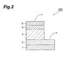
- a film obtained by the same film formation and surface treatment as in Examples 1, 3, 4, 5, 8, 9, 10, 11, 12 and 13, and Comparative Examples 1 to 6 was used to prepare a solar cell 100 illustrated in Figure 2 , and evaluation was performed.
- a translucent insulating base plate (1) a non-alkali glass base plate with a smooth surface was used.
- a transparent conductive film as a surface electrode layer (2) was formed on the main surface of the translucent insulating base plate (1) by the magnetron sputtering method. Then, the surface of the surface electrode layer (2) was subjected to the surface treatment. Characteristics of the obtained transparent conductive film were the same as those shown in Tables 3 and 4.
- the p-i-n junction was obtained by forming a p layer, an i layer and an n layer in this order.
- Gases of silane, hydrogen and diborane were mixed and used at the time of forming the p layer, a silane gas was used at the time of forming the i layer, and gases of silane, hydrogen and phosphine were mixed and used at the time of forming the n layer.
- a zinc oxide film with 2% by weight of aluminum added was formed as a barrier layer (4) by the magnetron sputtering method under an argon atmosphere of an oxygen partial pressure of 0.1 % or less at a base plate heating temperature of 100°C, a sputtering pressure of 0.4 Pa and an input power of 150 W so that the thickness was 50 nm.
- an Ag film was formed as a rear surface electrode layer (5) using an Ag target by the magnetron sputtering method at room temperature under an argon atmosphere of an oxygen partial pressure of 0.1 % or less at a sputtering pressure of 0.4 Pa and an input power of 100 W so that the thickness was about 300 nm.
- a superstrate type thin film silicon solar cell 100 in which light is incident from the side of the translucent insulating base plate (1) was prepared.
- a current at the time of short circuit of both electrodes is referred to as a short circuit current
- an output voltage at the time of opening of both electrodes is referred to as an open voltage
- a value obtained by dividing the short circuit current by an effective light receiving area is referred to as a short circuit current density.
- the product of the short circuit current and the open voltage is a power value to be ideally extracted in this solar cell, and it is a fill factor (FF) that represents a ratio of an actually extractable power to the value.
- the conversion efficiency is represented by a ratio of an actually extracted power to the output of incident light (100 mW/cm 2 ) (short circuit current density ⁇ open voltage ⁇ fill factor). Therefore, the larger values of the short circuit current density, open voltage, fill factor and conversion efficiency allow the solar cell to have more excellent characteristics.
- 1 translucent insulating base plate
- 2 surface electrode layer
- 3 photoelectric conversion layer
- 4 barrier layer
- 5 rear surface electrode layer
- 10 transparent conductive film
- 100 solar cell
- a concave lens-like texture (first texture)
- b concave lens-like texture (second texture)
- Wa width of concave lens-like texture a
- Wb width of concave lens-like texture b
- Ha depth of concave lens-like texture a
- Hb depth of concave lens-like texture b.
Landscapes
- Chemical & Material Sciences (AREA)
- Engineering & Computer Science (AREA)
- Metallurgy (AREA)
- Chemical Kinetics & Catalysis (AREA)
- Materials Engineering (AREA)
- Mechanical Engineering (AREA)
- Organic Chemistry (AREA)
- Manufacturing & Machinery (AREA)
- Non-Insulated Conductors (AREA)
- Physical Vapour Deposition (AREA)
- Manufacturing Of Electric Cables (AREA)
- Photovoltaic Devices (AREA)
- Light Receiving Elements (AREA)
Abstract


Description
- The present invention relates to a transparent conductive zinc oxide based film, a method for production thereof and use thereof, and specifically a transparent conductive film having a surface shape useful as an optical device or an electron device and a method for production thereof.
- In optical devices and electron devices such as a solar cell, a photodiode, a flat panel display (FPD) and a light-emitting diode (LED), in order to maximally extract their characteristics, a technique for diffusing light is an essential technique, and in particular, a technique for improving light scattering ability at all wavelength regions is essential. As such an approach for scattering light, there are mainly two approaches, which are, for example, as described in Patent Literature 1:
- (1) an approach for forming fine asperities (hereinafter, textures) on a surface to increase surface roughness, thereby causing optical scattering; and
- (2) an approach for causing scattering by a flat surface and a built-in optical scattering element.
- It has been hitherto examined to allow the surface of a transparent conductive film to have various shapes using this approach in order to improve light scattering ability. For example, in
Patent Literature 2, a surface roughness has been increased by adjusting film formation conditions to accomplish a high light scattering ability. In order to exceed this, inPatent Literature 3, light scattering ability has been improved by providing fine mountain-like relieves on the surface of a transparent conductive film and forming a plurality of finer asperities on each mountain. - Recently, surface textures suitable for improving the light scattering ability of a transparent conductive film have been found, and for example, it has been reported in
Non Patent Literature 1 that concave lens-like textures of a single size are formed on the surface of a thin film to thereby obtain more favorable light scattering ability than the mountain-like textures. In this method, the concave lens-like textures are formed by subjecting a transparent conductive film once formed to etching by an acid. - On the other hand, with respect to such concave lens-like textures, it has been reported in
Patent Literature 1 that a plurality of lenses of several µm are prepared on the inner curved surface of a lens of several tens of µm to make it possible to further improve light scattering ability. However, in this Literature, since the textures are formed by molding on a polymer surface using a mold, it is difficult to perform microfabrication below several µm, and a base material on which the textures can be formed has been limited to polymers. Therefore, a method for more finely and complicatedly forming the concave lens-like textures on the surface of a substrate is required in order to impart a higher light scattering ability to a transparent conductive film. - Furthermore, even in the case of forming the concave lens-like textures of a single size on a transparent conductive film, it is necessary to regulate the temperature of a base plate to 300°C or higher in order to ensure the transparency of the transparent conductive film, and thus the base plate on which the transparent conductive film is formed is limited to materials (glass, metal plate, ceramics and the like) that can withstand high temperatures. If it is possible to reduce such a film formation temperature, it enables film formation on a base plate using an organic substance such as a polymer, thereby enabling the selectivity of material of a base plate to be considerably extended.
-
- Patent Literature 1: Japanese Patent Application Laid-Open No.
2003-270413 - Patent Literature 2: Japanese Patent Application Laid-Open No.
2005-002387 - Patent Literature 3: International Publication No.
WO 2003/036657 - Non Patent Literature 1: M. Berginski et al., J Appl Phys., 101. 074903. (2007)
- Although a moderately high light scattering ability has been obtained at the visible light region even in the conventional concave lens-like texture, it is necessary to improve light scattering ability at the near-infrared region in addition to further improving light scattering ability at the visible light region, in order to further improve the performances of the above devices. In addition, in order to remarkably extend the material selectivity, it is demanded to lower the temperature in a production process. It is further demanded for a transparent conductive film that solves these problems to hold a high durability.
- In order to solve the foregoing problems, the present invention aims to provide a transparent conductive zinc oxide based film that can lower the temperature in a production process while precisely controlling fine structures of surface textures and accomplishing a high light scattering ability and a high durability, and a method for production thereof and use thereof.
- The present inventors have intensively studied about the above problems, and as a result, have reached the present invention. That is, the present invention is as follows.
- (1) A transparent conductive zinc oxide based film containing Ti, Al and Zn in such a proportion that satisfies the following formulae (1), (2) and (3) in terms of atomic ratio, and having a plurality of surface textures different in size on a surface, wherein a center-line average surface roughness Ra of the surface is 30 nm to 200 nm, and an average value of widths of the surface textures is 100 nm to 10 µm.


- (2) The transparent conductive film according to (1), wherein a surface area of the transparent conductive film is 101 µm2 to 200 µm2 per region of 10 µm × 10 µm.
- (3) The transparent conductive film according to (1) or (2), wherein a shape of the surface textures is a concave lens-like shape.
- (4) The transparent conductive film according to any one of (1) to (3), wherein a shape of the surface textures is a concave lens-like shape, an average value of ratios of widths of the surface textures to depths of the surface textures is 1 to 5, and at least part of the plurality of surface textures share a boundary with each other and are randomly arranged.
- (5) The transparent conductive film according to (3) or (4), wherein the surface textures comprise first textures having a concave lens-like shape and second textures having a concave lens-like shape, the second textures are present inside the first textures, an average value of widths of the second textures is smaller than an average value of widths of the first textures, and an average value of the ratios of the widths of the surface textures to the depths of the surface textures is 1 to 5.
- (6) A method for producing of the transparent conductive film according to any one of (1) to (5) described above, comprising a step of forming a film on a heated base material by a sputtering method using a zinc oxide based target containing Ti, Al and Zn in such a proportion that satisfies the following formulae (1), (2) and (3) in terms of atomic ratio, and a step of subjecting a surface of the formed film to a surface treatment.


- (7) The method for production according to (6), wherein a temperature of the heated base material is 250°C or lower.
- (8) The method for production according to (6) or (7), wherein the surface treatment is wet etching using an acid whose hydrogen ion concentration is 0.001 to 0.20 mol/l.
- (9) A substrate having a base material, and the transparent conductive film according to any one of (1) to (5) described above arranged on the base material.
- (10) An electron device or optical device comprising the substrate according to (9) described above.
- (11) A photoelectric conversion device comprising the substrate according to (9) described above.
- (12) A solar cell having the transparent conductive film according to any one of (1) to (5) described above.
- According to the present invention, it is possible to obtain a transparent conductive film having a specified surface shape, thereby making it possible to impart a high light scattering ability at a wide wavelength region (for example, the visible light region and the near-infrared region). Accordingly, the present invention can be variously applied to optical devices or electron devices such as a solar cell, a photodiode and an FPD backlight diffuser. In addition, since the present invention can obtain a transparent conductive film even by forming a film at the base material temperature of 200°C or lower, the present invention can also be applied to a flexible base plate on which a film is required to be formed at a low temperature, to thereby make it possible to remarkably extend the material selectivity. Furthermore, the present invention can obtain the above effects while keeping the durability of the transparent conductive film high.
-
- [
Figure 1] Figure 1 is a schematic view of a cross section of a transparent conductive film according to the present embodiment. - [
Figure 2] Figure 2 is a schematic view of a solar cell prepared in Example. - Hereinafter, a detail of an embodiment of the present invention will be described. A transparent conductive film according to the present embodiment (transparent conductive zinc oxide based film) has a specified composition and surface shape, and contains Ti and Al in a predetermined proportion in terms of atomic ratio, wherein a center-line average surface roughness Ra is 30 nm or more and 200 nm or less, the transparent conductive film has textures different in size on the surface, and the average value of the widths of the textures is 100 nm to 10 µm. In the present embodiment, it is possible to adjust the sheet resistance of the transparent conductive film to 100 Ω/□ or less. Herein, the "Ω/□" means "ohm/square". In the present embodiment, it is possible to adjust the average transmittance of the transparent conductive film at a film thickness of 1 µm to 50% or more at wavelengths of 400 nm to 800 nm.
- The transparent conductive film according to the present embodiment contains Ti, Al and Zn in such a proportion that satisfies the following formulae (1), (2) and (3) in terms of atomic ratio.


- If Al/(Zn + Al + Ti) in the above formula (1) is less than 0.001, the resistance of the film remarkably rises and also, any textures exhibiting a high light scattering ability cannot be obtained. If Al/(Zn + Al + Ti) in the above formula (1) exceeds 0.079, the resistance of the film increases, and any textures exhibiting a high light scattering ability cannot be obtained. If Ti/(Zn + Al + Ti) in the above formula (2) is less than 0.001, weatherability remarkably deteriorates and also, any textures exhibiting a high light scattering ability cannot be obtained when producing the film at a low temperature. If Ti/(Zn + Al + Ti) in the above formula (2) exceeds 0.079, the resistance of the film remarkably increases, and any textures exhibiting a high light scattering ability cannot be obtained. If (Ti + Al)/(Zn + Al + Ti) in the above formula (3) is less than 0.010, the resistance of the film rises, and any textures exhibiting a high light scattering ability cannot be obtained. If (Ti + Al)/(Zn + Al + Ti) in the above formula (3) exceeds 0.080, the resistance of the film rises and also, any textures exhibiting a high light scattering ability cannot be formed.
- It is preferable that the transparent conductive film according to the present embodiment contain Ti, Al and Zn in such a proportion that satisfies the following formulae (4) and (5) in terms of atomic ratio.


It is more preferable that the transparent conductive film according to the present embodiment contain Ti, Al and Zn in such a proportion that satisfies the following formulae (6) and (7) in terms of atomic ratio.

- The transparent conductive film according to the present embodiment has a plurality of textures (surface textures) different in size on the surface of the transparent conductive film. Herein, the "textures" mean the fine asperities of the surface as described above, and the shape of the textures is not particularly limited and examples of the shape includes a concave lens-like shape, a V-shaped recessed part, a mountain-shaped convex part and a spike-like shape. The "size" of the texture means the depth and width of a concave part, and the height and width of a convex part.
- In the present embodiment, the average value of the widths of the textures is 100 nm to 10 µm, preferably 200 nm to 5 µm, and more preferably 300 nm to 3 µm. If the average value of the widths of the textures is less than 100 nm, sufficient light scattering ability cannot be achieved. If the average value of the widths of the textures exceeds 10 µm, the flatness of the film is too high, and light scattering ability deteriorates. Herein, the "widths of the textures" means a value at which a distance between two parallel straight lines in contact with a texture when the two straight lines sandwich one texture is maximum. The "average value of the widths of the textures" is that obtained by selecting an arbitrary 25-/µm2 section on the main surface of the transparent conductive film and determining the average of the widths of the whole textures present in the section. Herein, the "25-/µm2 section" is a region surrounded by a square of 5 µm × 5 µm.
- As in the present embodiment, the thin film on which textures different in size have been formed on the surface thereof exhibits a higher scattering ability than that of the thin film on which textures of a specified single size have been formed.
- The center-line average surface roughness Ra of the surface (main surface) of the transparent conductive film according to the present embodiment is 30 nm to 200 nm, preferably 40 nm to 150 nm, and more preferably 50 nm to 150 nm. If the center-line average surface roughness Ra is less than 30 nm, the shape of the textures is not suitable for light scattering, and light scattering ability deteriorates. If the center-line average surface roughness Ra exceeds 200 nm, the shape of the textures is precipitous to thereby make it difficult for formation of a laminate film, thereby adversely affecting device characteristics.
- The root mean square roughness Rms of the surface (main surface) of the transparent conductive film according to the present embodiment is not particularly limited, and is preferably 50 nm to 450 nm and more preferably 60 nm to 300 nm. If the root mean square roughness Rms is less than 50 nm, the shape of the textures is not suitable for light scattering, and light scattering ability tends to deteriorate. If the root mean square roughness Rms exceeds 450 nm, the shape of the textures is precipitous to thereby make it difficult for formation of a laminate film, thereby tending to adversely affect device characteristics.
- The surface area of the transparent conductive film according to the present embodiment is preferably 101 µm2 to 200 µm2 and more preferably 105 µm2 to 150 µm2, per 100-µm2 section. Herein, the "100-µm2 section" is a region surrounded by a square of 10 µm × 10 µm. If the surface area of the transparent conductive film exceeds 200 µm2, a film with a large number of fine voids on the surface thereof is formed, and when forming a laminate film, namely, forming an upper layer film on the transparent conductive film as a lower layer film, such a phenomenon that the transparent conductive film penetrates through the upper layer film may occur and film growth may be adversely affected at the time of formation of the upper layer film formed on the transparent conductive film as the lower layer film. As a result, it may adversely affect the performances of an optical device, an electron device and the like. If the surface area of the transparent conductive film is less than 101 µm2, any defined textures are not formed and light scattering ability is extremely low in some cases.
- In the present embodiment, it is preferable that the shape of the textures be a concave lens-like shape. Hereinafter, concave lens-like textures (hereinafter, optionally referred to as "concave lenses") will be described in detail. The concave lens-like textures act as small lenses that deflect light passing through the transparent conductive film. The shape of the concave lens-like textures is not particularly limited, and the curved shape thereof in the depth direction is an arc-like shape, but does not necessarily need to be a completely arc-like shape. The shape of the concave lenses viewed from directly above does not need to be a completely circular shape.
- In the present embodiment, the average value of the width/depth of the concave lenses is preferably 1 to 5, and more preferably 1 to 3. If the average value of the width/depth of the concave lenses is less than 1, an angle made by the curved surface of the concave lens and the base material is large to induce the total reflection at the curved surface of the concave lens and thus light scattering ability tends to deteriorate, and if the average value of the width/depth of the concave lenses exceeds 5, curvature for effectively scattering light is small and thus light scattering ability tends to deteriorate. Herein, the width/depth of the concave lenses means the ratio of the width of the concave lens to the depth of the concave lens (width of concave lens/depth of concave lens). The "depth of the concave lens" denotes the difference in height between the point located at the lowest position and the point located at the highest position in the thickness direction of the transparent conductive film, of one concave lens. The "width of the concave lens" means a value at which a distance between two straight lines when the two straight lines sandwich one concave lens (crater) is maximum. The value of the width/depth of the concave lens is one of the main factors for determining the light scattering ability that each lens has. The smaller value of the width/depth of the concave lens expresses that the lens is deeply and narrowly formed, and the larger value of the width/depth of the concave lens means that a shallow and flat lens is formed.
- The surface shape and configuration of the transparent conductive film according to the present embodiment is schematically described with reference to
Figure 1 . In a transparentconductive film 10 according to the present embodiment, as illustrated inFigure 1 , a plurality of concave lens-like textures share a boundary with each other and are randomly arranged on the surface of the film. In this case, further improvement in light scattering ability can be expected. Herein, the "sharing a boundary" means that the profile of one lens is in contact with the profile of the adjacent lens at one or more points. The "randomly arranged" means that the concave lenses are arranged without a particular regularity. Herein, with respect to the plurality of concave lens-like textures, it is preferable that at least part of the textures share a boundary with each other and are randomly arranged, and the textures may include textures without a boundary shared with their adjacent textures and textures arranged according to a particular regularity. It is preferable that the proportion of the total surface area of these concave lens-like textures to the surface area of the main surface of the transparent conductive film be 90% or more. Herein, it is more preferable that all the plurality of the concave lens-like textures share a boundary with each other and are randomly arranged. - In order to further improve light scattering ability, it is preferable that the concave lens-like textures comprises first textures having a concave lens-like shape (hereinafter, referred to as "concave lens-like textures (a)") and second textures having a concave lens-like shape (hereinafter, referred to as "concave lens-like textures (b)") present inside (interior curved surface) the concave lens-like textures (a). It is preferable that one or more concave lens-like textures (b) be present on the film surface, and a plurality of the textures (b) may be present inside one concave lens-like texture (a). Furthermore, it is preferable that the transparent conductive film according to the present embodiment have a configuration in which the end of one concave lens-like texture (a) or concave lens-like texture (b) shares a boundary with other concave lens-like texture (a) or concave lens-like texture (b).
- The average value of the widths (lens widths, Wb in
Figure 1 ) of the concave lens-like textures (b) present inside the concave lens-like textures (a) is preferably smaller than the average value of the widths (lens widths, Wa inFigure 1 ) of the concave lens-like textures (a), and more preferably 80% or less to the average value of the widths of the concave lens-like textures (a). If the average value of the widths of the concave lens-like textures (b) exceeds 80% to the average value of the widths of the concave lens-like textures (a), the complexity of the textures deteriorates and thus light scattering ability tends to deteriorate. - It is preferable that the average value of the width/depth of the concave lenses (concave lens-like textures (a), (b)) formed on the film surface be 1 to 5. If the average value of the width/depth of the concave lenses exceeds 5, curvature for effectively scattering light is small and thus light scattering ability tends to deteriorate. If the average value of the width/depth of the concave lenses is less than 1, an angle made by the curved surface of the concave lens and the base material is large to induce the total reflection at the curved surface of the concave lens and thus light scattering ability tends to deteriorate. Herein, the depths of the concave lens-like textures (a), (b) are Ha, Hb as represented in
Figure 1 . - When various concave lenses in size share a boundary with each other and are randomly arranged to configure surface textures, further improvement in light scattering ability can be expected.
- The total number of the concave lens-like textures (a), (b) formed on the film surface is preferably 1.0 × 10⁶ to 5.0 × 10⁶ textures/mm2, and more preferably 2.0 × 10⁶ to 4.0 × 10⁶ textures/mm2, in total. With respect to the proportion of the concave lens-like textures (a), (b) in number, it is preferable that the proportion of the concave lens-like textures (a) be 10 to 80% and that of the concave lens-like textures (b) be 90 to 20%, and it is more preferable that that of the concave lens-like textures (a) be 30 to 70% and that of the concave lens-like textures (b) be 70 to 30%. It is to be noted that the total "the proportion of the concave lens-like textures (a) + the proportion of the concave lens-like textures (b)" is 100%.
- If the total number of the concave lens-like textures (a), (b) is less than 1.0 × 10⁶ textures/mm2, the complexity of the shape of the surface textures deteriorates and thus light scattering ability tends to deteriorate. If the total number of the concave lens-like textures (a), (b) exceeds 5.0 × 10⁶ textures/mm2, the size of each texture is small and light scattering ability tends to deteriorate. Furthermore, if the proportion of the concave lens-like textures (a), (b) is lopsided (the case where the proportion of the concave lens-like textures (a) does not satisfy 10 to 80%, or the case where the proportion of the concave lens-like textures (b) does not satisfy 90 to 20%), the complexity of the shape of the surface texture deteriorates and thus light scattering ability tends to deteriorate.
- In the present embodiment, the surface shape can be measured by the method described below. That is, the film surface is observed by a scanning electron microscope (SEM), an atomic force microscope (AFM) or a transmission electron microscope (TEM), and the obtained observation photograph can be used to analyze the widths and depths of the concave lenses, and the shape of the textures of the film surface, and to determine the number of the concave lenses formed on the surface, the concave lens size distribution, the surface roughness and the surface area.
- In the present embodiment, a haze rate (H) is used as a parameter for evaluating light scattering ability. The haze rate expresses an amount of light scattered by a sample to be evaluated, of transmitted light through the sample, and the higher haze rate means that the light scattering ability of the relevant substance is high. The haze rate is generally used as a parameter for evaluating light scattering. Herein, the haze rate is defined as follows by using the transmittance (Ta) and scattering transmittance (Td) of the sample.

- The haze rate of the thin film obtained in the present embodiment (average value at wavelengths of 400 nm to 600 nm) is preferably 40% or more, and more preferably 60% or more. The haze rate of the thin film obtained in the present embodiment may reach 90% or more (average value at wavelengths of 400 nm to 600 nm). In the thin film obtained in the present embodiment, it is preferable that the average value of the haze rates at 400 nm to 600 nm be 90% or more and the average value of the haze rates at 600 nm to 1000 nm be 50% or more.
- In the case of using the transparent conductive film for an optical device, an electron device and the like, the durability of the transparent conductive film is one of the important factors in determining the lifetime of the device. Therefore, from the viewpoint of extension in lifetime, it is preferable that the transparent conductive film has a high durability. The durability can be evaluated by the method described below. That is, a specimen is continuously exposed to an environment of a temperature of 85°C and a relative humidity of 85% for 1000 hours to observe a change in resistivity. At this time, when the resistivity before testing is defined as A and the resistivity after testing is defined as B, the value of (B-A)/A can be determined in terms of percentage unit to be defined as an index of the durability. Usually, the value tends to increase over testing time, and the smaller value indicates that the durability is more excellent.
- Then, a method for producing the transparent conductive film according to the present embodiment will be described. The method for producing the transparent conductive film according to the present embodiment comprises a film formation step of forming a transparent conductive zinc oxide based film on a heated base material (for example, base plate) by a sputtering method using a zinc oxide based target, and a surface treatment step of subjecting the surface of the formed film to a surface treatment. In the present embodiment, a transparent conductive film formed on a base material can be obtained and at the same time, a substrate having a base material, and the transparent conductive film arranged on the base material can be obtained.
- First, a method for forming a transparent conductive film in the film formation step will be described. In the present embodiment, a zinc oxide based target containing Ti, Al and Zn in such a proportion that satisfies the above formulae (1), (2) and (3) is used, and this target preferably contains Ti, Al and Zn in such a proportion that satisfies the following formulae (4) and (5) in terms of atomic ratio.


This target more preferably contains Ti, Al and Zn in such a proportion that satisfies the following formulae (6) and (7) in terms of atomic ratio.

- Such a target can be configured by using a sintered body obtained by mixing, molding and sintering a raw material powder having such a composition.
- As a method for forming a conductive thin film (transparent conductive film), it is preferable to use a sputtering method and in particular, it is more preferable to use a DC magnetron sputtering method. In order to form the surface textures by the surface treatment in the surface treatment step described later, it is preferable that the crystal structure of a thin film be oriented to (002) plane in the hexagonal system. Accordingly, it is preferable to form a film by a sputtering method in which the thin film oriented to (002) plane is relatively easily obtained.
- With respect to forming the conductive thin film on a heated base material by a sputtering method, and the temperature of the base material is not particularly limited. The temperature of the base material is preferably 250°C or lower, and more preferably 50°C to 200°C. With respect to a conventional transparent conductive zinc oxide based film which does not contain Ti and to which only Al is added in a small amount, a film sufficiently oriented to (002) plane cannot be obtained unless the base material is heated to 300°C or higher at the time of film formation, and the above concave lens-like textures were not able to be obtained even if the surface treatment was performed. In contrast, in the present embodiment that relates to a transparent conductive zinc oxide based film containing Ti and Al, by the surface treatment, it is possible to form a transparent conductive film having a light scattering ability equal to or higher than a conventional conductive thin film formed at such a high temperature that the base material temperature is 300°C or higher even when forming the film at a base material temperature of 250°C or lower.
- The film formation is usually performed under an Ar atmosphere condition of an O2 partial pressure of 1% or less, preferably 0.1% or less. If the O2 partial pressure exceeds 1%, it tends to be difficult to obtain a desired texture.
- The sputtering pressure is preferably 0.2 to 1.0 Pa, and more preferably 0.2 to 0.6 Pa. By performing the film formation within such pressure range using a zinc oxide target with Ti and Al added, the film oriented to (002) plane is easily obtained. If the sputtering pressure exceeds 1.0 Pa, orientation tends to be inferior and thus it tends to be difficult to obtain a desired surface texture. If the sputtering pressure is less than 0.2 Pa, the number of the concave lenses formed by the surface treatment tends to remarkably decrease, thereby causing light scattering ability to deteriorate in some cases.
- The base material for use in the present embodiment is not particularly limited. For example, it is possible to form a conductive thin film on an inorganic base material made of metals such as aluminum, copper and stainless steel; ceramics such as alumina, titania and silicon carbide; glass, or the like, to thereby obtain a substrate. Also, since the film formation temperature can be set to 250°C or lower in the present embodiment, it is possible to form a conductive thin film on an organic base material made of PET (polyethylene terephthalate), PEN (polyethylene naphthalate), PES (polyether sulfone), COP (cycloolefin polymer), polyimide, a TAC (triacetylcellulose) film, an acrylic film, or the like, to thereby obtain a substrate. Herein, the "substrate" means a base material on which a thin film has been formed.
- For the surface treatment to which the surface of the formed film is subjected in the surface treatment step, it is possible to suitably use dry etching, wet etching and the like, and wet etching is preferable. In the wet etching, it is possible to use as an etching liquid, acids such as inorganic acids (sulfuric acid, hydrochloric acid, nitric acid, phosphoric acid and the like) and organic acids (acetic acid, oxalic acid, butyric acid, citric acid and the like), alkalis (hydroxides of alkali metals, hydroxides of alkali earth metals, and the like), or mixtures of various acids or mixtures of various alkalis. The etching liquid may be brought into contact with the film surface. Among the above etching liquids, it is preferable to use an acid whose hydrogen ion concentration is 0.001 to 0.20 mol/l, and it is more preferable to use hydrochloric acid as an acid. Hydrochloric acid is preferable because the size of the chloride ion of the hydrochloric acid is smaller than anions of other acids (for example, nitric acid, sulfuric acid and acetic acid).
- In the case of using hydrochloric acid as the etching liquid, the liquid temperature of the etching liquid can be set from room temperature to a temperature lower than the boiling point of hydrochloric acid. It is preferable that the liquid temperature of the etching liquid be 40°C to 50°C. This is because the slightly higher liquid temperature makes the difference between the etching rate in the (002) plane direction and the etching rate on other crystal planes larger to thereby easily form a texture shape suitable for light scattering.
- It is preferable that the etching be performed in multiple times, and it is preferable that a short time etching be repeated from the viewpoint of easily achieving a high haze rate.
- If the hydrogen ion concentration of the acid exceeds 0.20 mol/l, it may be difficult to control the etching rate and may be difficult to form the concave lens-like textures (b) to be formed inside the fine concave lens-like textures (a) on the surface. If the hydrogen ion concentration of the acid is less than 0.001 mol/l, the rate of the surface treatment may remarkably lower and the productivity in a production process may be remarkably inferior.
- The substrate thus obtained by the surface treatment is suitably applied to devices such as electron devices or optical devices for use in a solar cell, a photodiode, a photosensor, a flat panel display, a light-emitting diode, a liquid crystal display, a phototransduction apparatus and the like. In addition, this substrate is suitably used in a photoelectric conversion device. In the photoelectric conversion device using this substrate, since light that has reached the device is scattered by the texture structure in the present embodiment, a vertical reflection can be reduced to further increase light incident inside the device. In addition, since the incident light at this time is obliquely incident to the device, the light path length thereof is longer than the case of being vertically incident to the device. This results in making it possible to convert more light to current and to accomplish a high conversion efficiency.
- Hereinafter, the present invention will be described in more detail with reference to Examples, but the present invention is not limited to these Examples.
- The number of textures, transmittance and haze rate were recorded as average values by performing each Example five times. The value of the width/depth of the concave lenses shows an average value of values with respect to respective concave lenses observed by AFM, wherein the average value was that determined by selecting an arbitrary 25-µm2 section and determining the average of the values of the whole concave lenses present therein. Herein, it was confirmed by an X-ray diffraction measurement that the crystal structure of the formed transparent conductive film is oriented to (002) plane in the hexagonal system. The measurement conditions are as follows: X-ray source: CuKa, output of X-ray source: 40 kV, 40 mA, and scanning rate: 1°/min.
- As a sputtering target, one prepared by mixing and molding respective powders of ZnO, TiO2 and Al2O3 so that the atomic ratio satisfied those shown in Table 1, then sintering them at 1200°C, and joining the obtained sintered body to a backing plate was used. DC magnetron sputtering was performed under the sputtering conditions of a glass base plate temperature of 200°C, an oxygen partial pressure of 0.1% or less, an argon atmosphere, a sputtering pressure of 0.4 Pa and an input power of 300 W, to thereby produce a film (transparent conductive zinc oxide based film) with a film thickness of 1 µm.
- This film was immersed in hydrochloric acid (liquid temperature: 40°C) with a hydrogen ion concentration of 0.17 mol/l for 20 seconds and then dried once. Furthermore, the etching was performed two times for 5 seconds, that is, etching was performed for 30 seconds in total, to thereby carry out the surface treatment (Table 2). After such etching, the surface shape was observed by SEM, TEM and AFM. The transmittance and haze rate were measured by using a spectrometer (manufactured by Hitachi High-Technologies Corporation, U-4100), and shown as average values at respective wavelength regions. The sheet resistance value was measured by using a Hall effect measurement apparatus, HL55WIN (BioRad Laboratories, Inc.). The results are shown in Tables 3 and 4.
- The durability of each film was examined as follows. That is, a specimen was continuously exposed to an environment of a temperature of 85°C and a relative humidity of 85% for 1000 hours to observe a change in resistivity. At this time, when the resistivity before testing was defined as A and the resistivity after testing was defined as B, the value of (B-A)/A was determined in terms of percentage unit to be defined as an index of the durability. Usually, the value tends to increase over testing time, and the smaller value indicates that the durability is more excellent. The results are shown in Table 3.
- A target was prepared by blending respective powders of ZnO, TiO2 and Al2O3 so that the atomic ratio satisfied those shown in Table 1, and subjected to the same film formation, surface treatment and evaluation as in Example 1. Herein, the solution for use in etching was a mixed solution of phosphoric acid/acetic acid (1:1= mol/mol) in which the hydrogen ion concentration was 0.05 mol/l. The results are shown in Tables 3 and 4.
- A target was prepared by blending respective powders of ZnO, TiO2 and Al2O3 so that the atomic ratio satisfied those shown in Table 1, and subjected to the same film formation, surface treatment and evaluation as in Example 1. Herein, the solution for use in etching was a hydrochloric acid solution in which the hydrogen ion concentration was 0.05 mol/l. The results are shown in Tables 3 and 4.
- A target was prepared by blending respective powders of ZnO, TiO2 and Al2O3 so that the atomic ratio satisfied those shown in Table 1, and subjected to the same film formation, surface treatment and evaluation as in Example 1. Herein, the base plate temperature at the time of film formation was 100°C. The results are shown in Tables 3 and 4.
- A target was prepared by blending respective powders of ZnO, TiO2 and Al2O3 so that the atomic ratio satisfied those shown in Table 1, and subjected to the same film formation, surface treatment and evaluation as in Example 1. Herein, in the etching method, it was immersed in the solution for 20 seconds and then dried, and the etching was repeatedly performed seven times for 5 seconds, that is, etching was performed for 55 seconds in total (20 seconds + 5 seconds × 7 times), to thereby carry out the surface treatment. The results are shown in Tables 3 and 4.
- A target was prepared by blending respective powders of ZnO, TiO2 and Al2O3so that the atomic ratio satisfied those shown in Table 1, and subjected to the same film formation, surface treatment and evaluation as in Example 1. Herein, the sputtering pressure was 4 Pa. The results are shown in Tables 3 and 4. In the obtained film, spike-like textures different in size were observed, and 90% of the textures fell within a range from 30 nm to 500 nm in height and from 100 nm to 1000 nm in width. With respect to the spike-like textures, the differences in height were up to 500 nm and the average of the distances between the tops of the spikes was 500 nm, and the curved surface was reduced as compared with the textures of Example 3.
- A target was prepared by blending respective powders of ZnO and Al2O3 so that the atomic ratio satisfied those shown in Table 1, and subjected to the same film formation, surface treatment and evaluation as in Example 1. The results are shown in Tables 3 and 4.
- A target was prepared by blending respective powders of ZnO and Ga2O3 so that the atomic ratio satisfied those shown in Table 1, and subjected to the same film formation, surface treatment and evaluation as in Example 1. The results are shown in Tables 3 and 4.
- A target was prepared by blending respective powders of ZnO and Al2O3 so that the atomic ratio satisfied those shown in Table 1, and subjected to the same film formation, surface treatment and evaluation as in Example 1. The results are shown in Tables 3 and 4. In the obtained film, spike-like textures different in size were observed, and 90% of the textures fell within a range from 30 nm to 350 nm in height and from 80 nm to 1000 nm in width. With respect to the spike-like textures, the differences in height were up to 350 nm and the average of the distances between the tops of the spikes was 400 nm, and the curved surface was reduced as compared with the textures of Example 3.
- A target was prepared by blending respective powders of ZnO, TiO2 and Al2O3 so that the atomic ratio satisfied those shown in Table 1, and subjected to the same film formation, surface treatment and evaluation as in Example 1. Herein, the base plate temperature at the time of film formation was 300°C. The results are shown in Tables 3 and 4.
- Each target was prepared by blending respective powders of ZnO, TiO2 and Al2O3 so that the atomic ratio satisfied those shown in Table 1, and subjected to the same film formation, surface treatment and evaluation as in Example 1. The results are shown in Tables 3 and 4.
- Each target was prepared by blending respective powders of ZnO, TiO2 and Ga2O3 so that the atomic ratio satisfied those shown in Table 1, and subjected to the same film formation, surface treatment and evaluation as in Example 1. The results are shown in Tables 3 and 4.
- A film obtained by the same film formation and surface treatment as in Examples 1, 3, 4, 5, 8, 9, 10, 11, 12 and 13, and Comparative Examples 1 to 6 was used to prepare a
solar cell 100 illustrated inFigure 2 , and evaluation was performed. - That is, as a translucent insulating base plate (1), a non-alkali glass base plate with a smooth surface was used. A transparent conductive film as a surface electrode layer (2) was formed on the main surface of the translucent insulating base plate (1) by the magnetron sputtering method. Then, the surface of the surface electrode layer (2) was subjected to the surface treatment. Characteristics of the obtained transparent conductive film were the same as those shown in Tables 3 and 4.
- Next, a photoelectric conversion layer (3) with a thickness of about 500 nm, having a p-i-n junction, was laminated by forming an a-Si:H film on the surface electrode layer (2) by using silane (SiH4), hydrogen, diborane (B2H6) or phosphine (PH3) as a raw material at a base plate heating temperature of 180°C by a plasma CVD method. Herein, the p-i-n junction was obtained by forming a p layer, an i layer and an n layer in this order. Gases of silane, hydrogen and diborane were mixed and used at the time of forming the p layer, a silane gas was used at the time of forming the i layer, and gases of silane, hydrogen and phosphine were mixed and used at the time of forming the n layer.
- Next, a zinc oxide film with 2% by weight of aluminum added was formed as a barrier layer (4) by the magnetron sputtering method under an argon atmosphere of an oxygen partial pressure of 0.1 % or less at a base plate heating temperature of 100°C, a sputtering pressure of 0.4 Pa and an input power of 150 W so that the thickness was 50 nm. Finally, an Ag film was formed as a rear surface electrode layer (5) using an Ag target by the magnetron sputtering method at room temperature under an argon atmosphere of an oxygen partial pressure of 0.1 % or less at a sputtering pressure of 0.4 Pa and an input power of 100 W so that the thickness was about 300 nm. According to the foregoing procedure, a superstrate type thin film silicon
solar cell 100 in which light is incident from the side of the translucent insulating base plate (1) was prepared. - Current-voltage characteristics when irradiating the obtained solar cell with light of AM 1.5 (100 mW/cm2) by a solar simulator were measured, and a short circuit current, open voltage, fill factor and photoelectric conversion efficiency were evaluated. Each result was converted to a relative value, assuming that the value obtained by using the zinc oxide film with only aluminum added (Comparative Example 1) as the surface electrode layer (2) was defined as 1.00, as conventionally used, and shown in Table 5.
- Herein, upon the light irradiation, a current at the time of short circuit of both electrodes is referred to as a short circuit current, an output voltage at the time of opening of both electrodes is referred to as an open voltage, and a value obtained by dividing the short circuit current by an effective light receiving area is referred to as a short circuit current density. The product of the short circuit current and the open voltage is a power value to be ideally extracted in this solar cell, and it is a fill factor (FF) that represents a ratio of an actually extractable power to the value. The conversion efficiency is represented by a ratio of an actually extracted power to the output of incident light (100 mW/cm2) (short circuit current density × open voltage × fill factor). Therefore, the larger values of the short circuit current density, open voltage, fill factor and conversion efficiency allow the solar cell to have more excellent characteristics.
-
[Table 1] Raw material powder Composition (atomic ratio) Zn/ (Zn+M+Ti) Element M M/ (Zn+M+Ti) Ti/ (Zn+M+Ti) Example 1 0.986 Al 0.009 0.005 Example 2 0.988 Al 0.004 0.008 Example 3 0.982 Al 0.008 0.010 Example 4 0.966 Al 0.010 0.024 Example 5 0.971 Al 0.017 0.012 Example 6 0.981 Al 0.003 0.016 Example 7 0.974 Al 0.007 0.019 Example 8 0.945 Al 0.008 0.047 Example 9 0.982 Al 0.008 0.010 Example 10 0.982 Al 0.008 0.010 Example 11 0.982 Al 0.008 0.010 Example 12 0.982 Al 0.008 0.010 Example 13 0.982 Al 0.008 0.010 Comparative Example 1 0.965 Al 0.035 0.000 Comparative Example 2 0.965 Ga 0.035 0.000 Comparative Example 3 0.990 Al 0.010 0.000 Comparative Example 4 0.982 Al 0.008 0.010 Comparative Example 5 0.914 Al 0.058 0.028 Comparative Example 6 0.913 Al 0.029 0.058 Comparative Example 7 0.982 Ga 0.008 0.010 Comparative Example 8 0.971 Ga 0.017 0.012 -
[Table 2] Film characteristics Composition ratio (atomic ratio) Film formation pressure (Pa) Film formation temperature (°C) Surface treatment Zn/ (Zn+M+Ti) Element M M/ (Zn+M+Ti) Ti/ (Zn+M+Ti) Type Hydrogen ion concentration (mol/L) Solution temperature (°C) Example 1 0.984 Al 0.010 0.006 0.4 200.0 Hydrochloric acid 0.17 40 Example 2 0.983 Al 0.005 0.012 0.4 200.0 Hydrochloric acid 0.17 40 Example 3 0.978 Al 0.010 0.012 0.4 200.0 Hydrochloric acid 0.17 40 Example 4 0.963 Al 0.011 0.026 0.4 200.0 Hydrochloric acid 0.17 40 Example 5 0.968 Al 0.019 0.013 0.4 200.0 Hydrochloric acid 0.17 40 Example 6 0.979 Al 0.003 0.018 0.4 200.0 Hydrochloric acid 0.17 40 Example 7 0.972 Al 0.008 0.020 0.4 200.0 Hydrochloric acid 0.17 40 Example 8 0.940 Al 0.010 0.050 0.4 200.0 Hydrochloric acid 0.17 40 Example 9 0.978 Al 0.010 0.012 0.4 200.0 Phosphoric cid/Acetic acid (1:l=mol/mol) 0.05 40 Example 10 0.978 Al 0.010 0.012 0.4 200.0 Hydrochloric acid 0.05 40 Example 11 0.978 Al 0.010 0.012 0.4 100.0 Hydrochloric acid 0.17 40 Example 12 0.978 Al 0.010 0.012 0.4 200.0 Hydrochloric acid 0.17 40 Example 13 0.978 Al 0.010 0.012 4 200.0 Hydrochloric acid 0.17 40 Comparative Example 1 0.965 Al 0.035 0.000 0.4 200.0 Hydrochloric acid 0.17 40 Comparative Example 2 0.965 Ga 0.035 0.000 0.4 200.0 Hydrochloric acid 0.17 40 Comparative Example 3 0.980 Al 0.020 0.000 0.4 200.0 Hydrochloric acid 0.17 40 Comparative Example 4 0.978 Al 0.010 0.012 0.4 300.0 Hydrochloric acid 0.17 40 Comparative Example 5 0.910 Al 0.060 0.030 0.4 200.0 Hydrochloric acid 0.17 40 Comparative Example 6 0.910 Al 0.030 0.060 0.4 200.0 Hydrochloric acid 0.17 40 Comparative Example 7 0.978 Ga 0.010 0.012 0.4 200.0 Hydrochloric acid 0.17 40 Comparative Example 8 0.963 Ga 0.011 0.026 0.4 200.0 Hydrochloric acid 0.17 40 -
[Table 3] Haze rate (%) Transmittance (%) 400-600 nm 600-800 nm 800-1000 nm 400-600 nm 600-800 nm 800-1000 nm Example I 65 42 20 79 81 83 Example 2 64 44 32 81 82 79 Example 3 70 50 38 80 82 79 Example 4 62 41 17 81 80 69 Example 5 60 39 15 79 81 82 Example 6 63 45 26 80 82 47 Example 7 66 48 24 82 81 82 Example 8 59 40 21 80 82 52 Example 9 69 51 39 80 82 81 Example 10 65 49 30 81 83 80 Example 11 67 42 29 80 82 78 Example 12 83 55 42 84 85 85 Example 13 46 33 24 80 80 83 Comparative Example 1 21 18 18 83 82 73 Comparative Example 2 20 16 14 84 81 71 Comparative Example 3 49 31 23 79 81 81 Comparative Example 4 21 18 18 83 82 73 Comparative Example 5 22 15 12 84 78 51 Comparative Example 6 19 15 9 81 77 72 Comparative Example 7 69 52 32 80 83 80 Comparative Example 8 65 43 23 81 79 83 -
[Table 4] Film Characteristics Center-fine surface roughness Ra(nm) Root mean square roughness Rms(nm) Surface area (µ m2/100µ m2 resistance section) Sheet (Ω/□) Durability (%) Arrangement of concave lenses Contact state of concave state lenses of concaves lenses Width of concave lens-like texture Width/depth of concave lens Number and proportion of concave lens-like textures Average value Width of concave lens (a) Width concave lens (b) Total number (textures/mm2) Proportion of concave lenses (a)(%) Proportion of concave lenses (b)(%) Example 1 8 70 114 25 12.3 Random Contacting with adjacent lens at one or more points 300 nm 580 nm 150nm 2.4 4.2×10⁶ 35 65 Example 2 59 72 117 7.8 2.8 Random Contacting with adjacent lens at one or more points 930 nm 1200 nm 680 nm 3 3.7×10⁶ 48 52 Example 3 62 78 114 11 4.3 Random Contacting with adjacent lens at one or more points 890 nm 1240 nm 480 nm 3.3 2,2×10⁶ 54 46 Example 4 56 68 115 14 3.9 Random Contacting with adjacent lens at one or more points 1200 nm 1500 nm 690 nm 2.1 1.8×10⁶ 63 37 Example 5 52 65 115 9.4 7.4 Random Contacting with adjacent lens at one or more points 1350nm 1620 nm 870 nm 2.2 1.6×10⁶ 64 36 Example 6 56 66 113 20 3.0 Random Contacting with adjacent lens al one or more points 1020 nm 1480 nm 600 nm 2.9 2.5×10⁶ 48 52 Example 7 62 75 116 13 4.0 Random Contacting with adjacent lens at one or more points 1280 nm 1680 nm 810 nm 3.5 2.3×10⁶ 54 46 Example 8 57 70 116 19 3.0 Random Contacting with adjacent lens at one or more points 1530 nm 1930 nm 970 nm 5.8 1.2x10⁶ 58 42 Example 9 63 77 114 13 4.2 Random Contacting with adjacent lens at one or more points 1110 nm 1470 nm 650 nm 3.7 2.2×10⁶ 56 44 Example 10 59 80 116 11 4.1 Random Contacting with adjacent lens at one or more points 900 nm 1290 nm 400 nm 3.9 2.3×10⁶ 56 44 Example 11 60 84 115 7.1 3.1 Random Contacting with adjacent lens at one or more points 420 nm 700 nm 190 nm 3.4 2.7×10⁶ 45 55 Example 12 88 125 107 23 4.5 Random Contacting with adjacent lens at one or more points 780 nm 1080 nm 430 nm 1.5 2.2×10⁶ 54 46 Example 13 56 74 114 13 7.4 - - 500 nm - - - - - - Comparative Example 1 15 31 105 2.3 14.9 Random Contacting with adjacent lens at one or more points 250 nm 260 nm 80 nm 4.8 2.3×10⁵ 95 5 Comparative Example 2 13 26 107 4 40.5 Random Contacting with adjacent lens at one or more points 330 nm 350 nm 100 nm 4.7 1.9×10⁵ 91 9 Comparative Example 3 44 60 115 23 48.2 - - 400 nm - - - - - - Comparative Example 4 11 24 108 3.5 4.0 Random Contacting with adjacent lens at one or more points 1440 nm 1600 nm 250 nm 4.9 2.0×10⁵ 88 12 Comparative Example 5 13 25 104 12 32.2 Random Contacting with adjacent lens at one or more points 1670 nm 1810 nm 420 nm 4.7 1.5×10⁵ 90 10 Comparative Example 6 16 30 104 20 18.3 Random Contacting with adjacent lens at one or more points 1630 nm 1740 nm 490 nm 4.8 1.2×10⁵ 91 9 Comparative Example 7 65 73 111 9 47.2 Random Contacting with adjacent lens at one or more points 960 nm 1420 nm 480 nm 3.6 2.4×10⁶ 51 49 Comparative Example 8 60 70 111 15 38.3 Random Contacting with adjacent lens at one or more points 860 nm 1100 nm 450 nm 1.8 1.8×10⁶ 63 37 -
[Table 5] Solar cell characteristics Short circuit current density Open voltage Fill factor Conversion efficiency Isc Voc FF η Example 1 1.12 0.99 1.10 1.12 Example 3 1.15 1.00 1.11 1.16 Example 4 1.10 1.00 1.09 1.10 Example 5 1.10 1.00 1.07 1.09 Example 8 1.08 1.00 1.06 1.07 Example 9 1.14 1.00 1.11 1.14 Example 10 1.11 0.99 1.10 1.11 Example 11 1.13 1.00 1.11 1.13 Example 12 1.18 0.99 1.08 1.16 Example 13 1.05 1.00 1.03 1.04 Comparative Example 1 1.00 1.00 1.00 1.00 Comparative Example 2 0.98 0.99 1.00 0.97 Comparative Example 3 1.01 0.99 0.99 0.99 Comparative Example 4 0.95 0.99 0.98 0.92 Comparative Example 5 0.96 1.00 1.00 0.96 Comparative Example 6 0.92 0.98 0.98 0.90 - 1: translucent insulating base plate, 2: surface electrode layer, 3: photoelectric conversion layer, 4: barrier layer, 5: rear surface electrode layer, 10: transparent conductive film, 100: solar cell, a: concave lens-like texture (first texture), b: concave lens-like texture (second texture), Wa: width of concave lens-like texture a, Wb: width of concave lens-like texture b, Ha: depth of concave lens-like texture a, Hb: depth of concave lens-like texture b.
Claims (12)
- A transparent conductive zinc oxide based film, containing Ti, Al and Zn in such a proportion that satisfies the following formulae (1), (2) and (3) in terms of atomic ratio, and having a plurality of surface textures different in size on a surface,
a center-line average surface roughness Ra of the surface being 30 nm to 200 nm, and
an average value of widths of the surface textures being 100 nm to 10 µm.


- The transparent conductive film according to claim 1, wherein a surface area of the transparent conductive film is 101 µm2 to 200 µm2 per region of 10 µm × 10 µm.
- The transparent conductive film according to claim 1 or 2, wherein a shape of the surface textures is a concave lens-like shape.
- The transparent conductive film according to any one of claims 1 to 3, wherein
a shape of the surface textures is a concave lens-like shape,
an average value of ratios of widths of the surface textures to depths of the surface textures is 1 to 5, and
at least part of the plurality of surface textures share a boundary with each other and are randomly arranged. - The transparent conductive film according to claim 3 or 4, wherein
the surface textures comprise first textures having a concave lens-like shape and second textures having a concave lens-like shape,
the second textures are present inside the first textures,
an average value of widths of the second textures is smaller than an average value of widths of the first textures, and
an average value of ratios of widths of the surface textures to depths of the surface textures is 1 to 5. - A method for production of the transparent conductive film according to any one of claims 1 to 5, comprising:a step of forming a film on a heated base material by a sputtering method using a zinc oxide based target containing Ti, Al and Zn in such a proportion that satisfies the following formulae (1), (2) and (3) in terms of atomic ratio; anda step of subjecting a surface of the formed film to a surface treatment.


- The method for production according to claim 6, wherein a temperature of the heated base material is 250°C or lower.
- The method for production according to claim 6 or 7, wherein the surface treatment is wet etching using an acid whose hydrogen ion concentration is 0.001 to 0.20 mol/l.
- A substrate having a base material, and the transparent conductive film according to any one of claims 1 to 5 arranged on the base material.
- An electron device or optical device comprising the substrate according to claim 9.
- A photoelectric conversion device comprising the substrate according to claim 9.
- A solar cell having the transparent conductive film according to any one of claims 1 to 5.
Applications Claiming Priority (3)
| Application Number | Priority Date | Filing Date | Title |
|---|---|---|---|
| JP2010089285 | 2010-04-08 | ||
| JP2011049942A JP5830882B2 (en) | 2010-04-08 | 2011-03-08 | Zinc oxide-based transparent conductive film, method for producing the same, and use thereof |
| PCT/JP2011/058814 WO2011126074A1 (en) | 2010-04-08 | 2011-04-07 | Transparent conductive zinc oxide film, process for production thereof, and use thereof |
Publications (3)
| Publication Number | Publication Date |
|---|---|
| EP2557573A1 true EP2557573A1 (en) | 2013-02-13 |
| EP2557573A4 EP2557573A4 (en) | 2014-08-27 |
| EP2557573B1 EP2557573B1 (en) | 2016-05-04 |
Family
ID=44763009
Family Applications (1)
| Application Number | Title | Priority Date | Filing Date |
|---|---|---|---|
| EP11765974.8A Not-in-force EP2557573B1 (en) | 2010-04-08 | 2011-04-07 | Transparent conductive zinc oxide film, process for production thereof, and use thereof |
Country Status (7)
| Country | Link |
|---|---|
| US (1) | US9024176B2 (en) |
| EP (1) | EP2557573B1 (en) |
| JP (1) | JP5830882B2 (en) |
| KR (1) | KR101778824B1 (en) |
| CN (1) | CN102934175B (en) |
| TW (1) | TWI521551B (en) |
| WO (1) | WO2011126074A1 (en) |
Families Citing this family (8)
| Publication number | Priority date | Publication date | Assignee | Title |
|---|---|---|---|---|
| JP2012092003A (en) * | 2010-09-29 | 2012-05-17 | Tosoh Corp | Sintered composite oxide, manufacturing method therefor and transparent conductive oxide film obtained using the same |
| JP6265362B2 (en) * | 2012-02-27 | 2018-01-24 | 日東電工株式会社 | CIGS compound solar cell |
| JP5966483B2 (en) * | 2012-03-22 | 2016-08-10 | 東ソー株式会社 | Oxide transparent conductive film and method for producing the same, element obtained thereby, and solar cell |
| US10276749B2 (en) * | 2013-01-09 | 2019-04-30 | Sensor Electronic Technology, Inc. | Ultraviolet reflective rough adhesive contact |
| US9768357B2 (en) * | 2013-01-09 | 2017-09-19 | Sensor Electronic Technology, Inc. | Ultraviolet reflective rough adhesive contact |
| KR102149937B1 (en) * | 2013-02-22 | 2020-09-01 | 삼성전자주식회사 | Photoelectronic device and image sensor |
| CN108697804B (en) * | 2015-10-05 | 2022-11-15 | 德克萨斯州立大学董事会 | Micro-and nano-devices for the detection and treatment of cartilage damage |
| WO2017164209A1 (en) * | 2016-03-23 | 2017-09-28 | 三菱マテリアル株式会社 | Laminated transparent conductive film, laminated wiring film, and method for producing laminated wiring film |
Family Cites Families (10)
| Publication number | Priority date | Publication date | Assignee | Title |
|---|---|---|---|---|
| JPH0945140A (en) * | 1995-07-28 | 1997-02-14 | Sumitomo Metal Mining Co Ltd | Zinc oxide transparent conductive film |
| WO2003036657A1 (en) * | 2001-10-19 | 2003-05-01 | Asahi Glass Company, Limited | Substrate with transparent conductive oxide film and production method therefor, and photoelectric conversion element |
| JP4248793B2 (en) * | 2002-02-15 | 2009-04-02 | 独立行政法人産業技術総合研究所 | Method for manufacturing thin film solar cell |
| US6583936B1 (en) | 2002-03-11 | 2003-06-24 | Eastman Kodak Company | Patterned roller for the micro-replication of complex lenses |
| JP4178513B2 (en) | 2003-06-10 | 2008-11-12 | 富士電機ホールディングス株式会社 | Method for forming conductive thin film having texture structure |
| EP2025654B1 (en) * | 2006-06-08 | 2018-09-19 | Sumitomo Metal Mining Co., Ltd. | Target obtained from an oxide sintered body |
| CN102121092A (en) * | 2006-07-28 | 2011-07-13 | 株式会社爱发科 | Sputtering target |
| JP2009016179A (en) * | 2007-07-04 | 2009-01-22 | Kaneka Corp | Transparent conductive film, and manufacturing method thereof |
| JP5003600B2 (en) * | 2008-06-13 | 2012-08-15 | 住友金属鉱山株式会社 | Oxide sintered body, target, transparent conductive film obtained using the same, and conductive laminate |
| CN101629284B (en) | 2009-08-03 | 2011-01-26 | 北京航空航天大学 | Preparation method of aluminum-doped zinc oxide transparent conductive film by solvothermal method |
-
2011
- 2011-03-08 JP JP2011049942A patent/JP5830882B2/en active Active
- 2011-04-07 EP EP11765974.8A patent/EP2557573B1/en not_active Not-in-force
- 2011-04-07 US US13/639,347 patent/US9024176B2/en not_active Expired - Fee Related
- 2011-04-07 KR KR1020127029032A patent/KR101778824B1/en not_active Expired - Fee Related
- 2011-04-07 CN CN201180028345.2A patent/CN102934175B/en not_active Expired - Fee Related
- 2011-04-07 WO PCT/JP2011/058814 patent/WO2011126074A1/en not_active Ceased
- 2011-04-08 TW TW100112267A patent/TWI521551B/en not_active IP Right Cessation
Non-Patent Citations (2)
| Title |
|---|
| KLUTH O ET AL: "Texture etched ZnO:Al coated glass substrates for silicon based thin film solar cells", THIN SOLID FILMS, ELSEVIER-SEQUOIA S.A. LAUSANNE, CH, vol. 351, no. 1-2, 30 August 1999 (1999-08-30), pages 247-253, XP004183103, ISSN: 0040-6090, DOI: 10.1016/S0040-6090(99)00085-1 * |
| See also references of WO2011126074A1 * |
Also Published As
| Publication number | Publication date |
|---|---|
| WO2011126074A1 (en) | 2011-10-13 |
| TWI521551B (en) | 2016-02-11 |
| US20130048060A1 (en) | 2013-02-28 |
| CN102934175B (en) | 2016-03-02 |
| KR101778824B1 (en) | 2017-09-15 |
| EP2557573B1 (en) | 2016-05-04 |
| EP2557573A4 (en) | 2014-08-27 |
| JP5830882B2 (en) | 2015-12-09 |
| KR20130042485A (en) | 2013-04-26 |
| CN102934175A (en) | 2013-02-13 |
| JP2011231401A (en) | 2011-11-17 |
| US9024176B2 (en) | 2015-05-05 |
| TW201205602A (en) | 2012-02-01 |
Similar Documents
| Publication | Publication Date | Title |
|---|---|---|
| EP2557573B1 (en) | Transparent conductive zinc oxide film, process for production thereof, and use thereof | |
| Sharma et al. | High-performance radiation stable ZnO/Ag/ZnO multilayer transparent conductive electrode | |
| Saha et al. | Bandgap widening in highly conducting CdO thin film by Ti incorporation through radio frequency magnetron sputtering technique | |
| Sakthivel et al. | Studies on optoelectronic properties of magnetron Sputtered cadmium stannate (Cd2SnO4) thin films as alternative TCO materials for solar cell applications | |
| Wang et al. | Fabrication and characterization of sputtered Mg and F co-doped ZnO thin films with different substrate temperature for silicon thin-film solar cell applications | |
| Wang et al. | ITO films with different preferred orientations prepared by DC magnetron sputtering | |
| Kumar et al. | Investigations on opto-electronical properties of DC reactive magnetron sputtered zinc aluminum oxide thin films annealed at different temperatures | |
| Silva et al. | Morphological and electrical evolution of ZnO: Al thin filmsdeposited by RF magnetron sputtering onto glass substrates | |
| Mahmood et al. | Conductivity enhancement by fluorine doping in boron-doped ZnO thin films deposited by the electrospraying method | |
| TWI558830B (en) | Method of making a transparent conductive oxide layer | |
| Portillo-Cortez et al. | A novel soft deposition methodology for textured ZnO: Al thin films as efficient transparent conductive oxide layers | |
| US20130109124A1 (en) | Methods of making a transparent layer and a photovoltaic device | |
| Chu et al. | Effect of annealing temperature and atmosphere on aluminum-doped ZnO/Au/aluminum-doped ZnO thin film properties | |
| KR20120074276A (en) | Transparent conductive film and device comprising same | |
| Cho et al. | Nanoscale silver-based Al-doped ZnO multilayer transparent-conductive oxide films | |
| Kondratiev et al. | Low temperature sol-gel technique for processing Al-doped Zinc Oxide films | |
| KR101236039B1 (en) | Conductive laminate and manufacturing method thereof | |
| Hymavathi et al. | Structural, surface morphological and optical properties of Cr doped CdO thin films for optoelectronic devices | |
| Kavei et al. | Evaluation of surface roughness and nanostructure of indium tin oxide (ITO) films by atomic force microscopy | |
| KR20120021849A (en) | Method for preparing of azo thin film using electron-beam | |
| Liu et al. | Effect of Annealing Temperature on Optoelectronic Performance of F-and Al-codoped ZnO Thin Films for Photosensor Applications. | |
| Reddy et al. | Preparation and characterization of Nickel Oxide thin films by direct current reactive magnetron sputtering at different substrate temperatures | |
| Chu et al. | Study of Cu-based Al-doped ZnO multilayer thin films with different annealing conditions | |
| Li et al. | A microstructural study on the surface and interface of CdTe/CdS solar cells | |
| Bou et al. | Optical and electrical properties of structured multilayer with tunable transparency rate |
Legal Events
| Date | Code | Title | Description |
|---|---|---|---|
| PUAI | Public reference made under article 153(3) epc to a published international application that has entered the european phase |
Free format text: ORIGINAL CODE: 0009012 |
|
| 17P | Request for examination filed |
Effective date: 20121015 |
|
| AK | Designated contracting states |
Kind code of ref document: A1 Designated state(s): AL AT BE BG CH CY CZ DE DK EE ES FI FR GB GR HR HU IE IS IT LI LT LU LV MC MK MT NL NO PL PT RO RS SE SI SK SM TR |
|
| DAX | Request for extension of the european patent (deleted) | ||
| A4 | Supplementary search report drawn up and despatched |
Effective date: 20140725 |
|
| RIC1 | Information provided on ipc code assigned before grant |
Ipc: C23C 14/58 20060101ALI20140721BHEP Ipc: H01B 5/14 20060101AFI20140721BHEP Ipc: H01B 13/00 20060101ALI20140721BHEP Ipc: C23C 14/34 20060101ALI20140721BHEP Ipc: C23C 14/08 20060101ALI20140721BHEP |
|
| GRAP | Despatch of communication of intention to grant a patent |
Free format text: ORIGINAL CODE: EPIDOSNIGR1 |
|
| INTG | Intention to grant announced |
Effective date: 20160125 |
|
| RIN1 | Information on inventor provided before grant (corrected) |
Inventor name: IIGUSA, HITOSHI Inventor name: KURAMOCHI, HIDETO Inventor name: AKIIKE, RYO |
|
| GRAS | Grant fee paid |
Free format text: ORIGINAL CODE: EPIDOSNIGR3 |
|
| GRAA | (expected) grant |
Free format text: ORIGINAL CODE: 0009210 |
|
| AK | Designated contracting states |
Kind code of ref document: B1 Designated state(s): AL AT BE BG CH CY CZ DE DK EE ES FI FR GB GR HR HU IE IS IT LI LT LU LV MC MK MT NL NO PL PT RO RS SE SI SK SM TR |
|
| REG | Reference to a national code |
Ref country code: GB Ref legal event code: FG4D |
|
| REG | Reference to a national code |
Ref country code: CH Ref legal event code: EP |
|
| REG | Reference to a national code |
Ref country code: AT Ref legal event code: REF Ref document number: 797526 Country of ref document: AT Kind code of ref document: T Effective date: 20160515 |
|
| REG | Reference to a national code |
Ref country code: IE Ref legal event code: FG4D |
|
| REG | Reference to a national code |
Ref country code: DE Ref legal event code: R096 Ref document number: 602011026215 Country of ref document: DE |
|
| REG | Reference to a national code |
Ref country code: NL Ref legal event code: MP Effective date: 20160504 |
|
| REG | Reference to a national code |
Ref country code: LT Ref legal event code: MG4D |
|
| PG25 | Lapsed in a contracting state [announced via postgrant information from national office to epo] |
Ref country code: NL Free format text: LAPSE BECAUSE OF FAILURE TO SUBMIT A TRANSLATION OF THE DESCRIPTION OR TO PAY THE FEE WITHIN THE PRESCRIBED TIME-LIMIT Effective date: 20160504 Ref country code: NO Free format text: LAPSE BECAUSE OF FAILURE TO SUBMIT A TRANSLATION OF THE DESCRIPTION OR TO PAY THE FEE WITHIN THE PRESCRIBED TIME-LIMIT Effective date: 20160804 Ref country code: LT Free format text: LAPSE BECAUSE OF FAILURE TO SUBMIT A TRANSLATION OF THE DESCRIPTION OR TO PAY THE FEE WITHIN THE PRESCRIBED TIME-LIMIT Effective date: 20160504 Ref country code: FI Free format text: LAPSE BECAUSE OF FAILURE TO SUBMIT A TRANSLATION OF THE DESCRIPTION OR TO PAY THE FEE WITHIN THE PRESCRIBED TIME-LIMIT Effective date: 20160504 |
|
| REG | Reference to a national code |
Ref country code: AT Ref legal event code: MK05 Ref document number: 797526 Country of ref document: AT Kind code of ref document: T Effective date: 20160504 |
|
| PG25 | Lapsed in a contracting state [announced via postgrant information from national office to epo] |
Ref country code: SE Free format text: LAPSE BECAUSE OF FAILURE TO SUBMIT A TRANSLATION OF THE DESCRIPTION OR TO PAY THE FEE WITHIN THE PRESCRIBED TIME-LIMIT Effective date: 20160504 Ref country code: HR Free format text: LAPSE BECAUSE OF FAILURE TO SUBMIT A TRANSLATION OF THE DESCRIPTION OR TO PAY THE FEE WITHIN THE PRESCRIBED TIME-LIMIT Effective date: 20160504 Ref country code: ES Free format text: LAPSE BECAUSE OF FAILURE TO SUBMIT A TRANSLATION OF THE DESCRIPTION OR TO PAY THE FEE WITHIN THE PRESCRIBED TIME-LIMIT Effective date: 20160504 Ref country code: LV Free format text: LAPSE BECAUSE OF FAILURE TO SUBMIT A TRANSLATION OF THE DESCRIPTION OR TO PAY THE FEE WITHIN THE PRESCRIBED TIME-LIMIT Effective date: 20160504 Ref country code: RS Free format text: LAPSE BECAUSE OF FAILURE TO SUBMIT A TRANSLATION OF THE DESCRIPTION OR TO PAY THE FEE WITHIN THE PRESCRIBED TIME-LIMIT Effective date: 20160504 Ref country code: GR Free format text: LAPSE BECAUSE OF FAILURE TO SUBMIT A TRANSLATION OF THE DESCRIPTION OR TO PAY THE FEE WITHIN THE PRESCRIBED TIME-LIMIT Effective date: 20160805 Ref country code: PT Free format text: LAPSE BECAUSE OF FAILURE TO SUBMIT A TRANSLATION OF THE DESCRIPTION OR TO PAY THE FEE WITHIN THE PRESCRIBED TIME-LIMIT Effective date: 20160905 |
|
| PG25 | Lapsed in a contracting state [announced via postgrant information from national office to epo] |
Ref country code: IT Free format text: LAPSE BECAUSE OF FAILURE TO SUBMIT A TRANSLATION OF THE DESCRIPTION OR TO PAY THE FEE WITHIN THE PRESCRIBED TIME-LIMIT Effective date: 20160504 |
|
| PG25 | Lapsed in a contracting state [announced via postgrant information from national office to epo] |
Ref country code: RO Free format text: LAPSE BECAUSE OF FAILURE TO SUBMIT A TRANSLATION OF THE DESCRIPTION OR TO PAY THE FEE WITHIN THE PRESCRIBED TIME-LIMIT Effective date: 20160504 Ref country code: CZ Free format text: LAPSE BECAUSE OF FAILURE TO SUBMIT A TRANSLATION OF THE DESCRIPTION OR TO PAY THE FEE WITHIN THE PRESCRIBED TIME-LIMIT Effective date: 20160504 Ref country code: DK Free format text: LAPSE BECAUSE OF FAILURE TO SUBMIT A TRANSLATION OF THE DESCRIPTION OR TO PAY THE FEE WITHIN THE PRESCRIBED TIME-LIMIT Effective date: 20160504 Ref country code: EE Free format text: LAPSE BECAUSE OF FAILURE TO SUBMIT A TRANSLATION OF THE DESCRIPTION OR TO PAY THE FEE WITHIN THE PRESCRIBED TIME-LIMIT Effective date: 20160504 Ref country code: SK Free format text: LAPSE BECAUSE OF FAILURE TO SUBMIT A TRANSLATION OF THE DESCRIPTION OR TO PAY THE FEE WITHIN THE PRESCRIBED TIME-LIMIT Effective date: 20160504 |
|
| REG | Reference to a national code |
Ref country code: DE Ref legal event code: R097 Ref document number: 602011026215 Country of ref document: DE |
|
| PG25 | Lapsed in a contracting state [announced via postgrant information from national office to epo] |
Ref country code: PL Free format text: LAPSE BECAUSE OF FAILURE TO SUBMIT A TRANSLATION OF THE DESCRIPTION OR TO PAY THE FEE WITHIN THE PRESCRIBED TIME-LIMIT Effective date: 20160504 Ref country code: AT Free format text: LAPSE BECAUSE OF FAILURE TO SUBMIT A TRANSLATION OF THE DESCRIPTION OR TO PAY THE FEE WITHIN THE PRESCRIBED TIME-LIMIT Effective date: 20160504 Ref country code: SM Free format text: LAPSE BECAUSE OF FAILURE TO SUBMIT A TRANSLATION OF THE DESCRIPTION OR TO PAY THE FEE WITHIN THE PRESCRIBED TIME-LIMIT Effective date: 20160504 Ref country code: BE Free format text: LAPSE BECAUSE OF FAILURE TO SUBMIT A TRANSLATION OF THE DESCRIPTION OR TO PAY THE FEE WITHIN THE PRESCRIBED TIME-LIMIT Effective date: 20160504 |
|
| PLBE | No opposition filed within time limit |
Free format text: ORIGINAL CODE: 0009261 |
|
| STAA | Information on the status of an ep patent application or granted ep patent |
Free format text: STATUS: NO OPPOSITION FILED WITHIN TIME LIMIT |
|
| 26N | No opposition filed |
Effective date: 20170207 |
|
| PG25 | Lapsed in a contracting state [announced via postgrant information from national office to epo] |
Ref country code: SI Free format text: LAPSE BECAUSE OF FAILURE TO SUBMIT A TRANSLATION OF THE DESCRIPTION OR TO PAY THE FEE WITHIN THE PRESCRIBED TIME-LIMIT Effective date: 20160504 |
|
| PG25 | Lapsed in a contracting state [announced via postgrant information from national office to epo] |
Ref country code: MC Free format text: LAPSE BECAUSE OF FAILURE TO SUBMIT A TRANSLATION OF THE DESCRIPTION OR TO PAY THE FEE WITHIN THE PRESCRIBED TIME-LIMIT Effective date: 20160504 |
|
| REG | Reference to a national code |
Ref country code: CH Ref legal event code: PL |
|
| GBPC | Gb: european patent ceased through non-payment of renewal fee |
Effective date: 20170407 |
|
| REG | Reference to a national code |
Ref country code: IE Ref legal event code: MM4A |
|
| REG | Reference to a national code |
Ref country code: FR Ref legal event code: ST Effective date: 20171229 |
|
| PG25 | Lapsed in a contracting state [announced via postgrant information from national office to epo] |
Ref country code: FR Free format text: LAPSE BECAUSE OF NON-PAYMENT OF DUE FEES Effective date: 20170502 |
|
| PG25 | Lapsed in a contracting state [announced via postgrant information from national office to epo] |
Ref country code: LI Free format text: LAPSE BECAUSE OF NON-PAYMENT OF DUE FEES Effective date: 20170430 Ref country code: LU Free format text: LAPSE BECAUSE OF NON-PAYMENT OF DUE FEES Effective date: 20170407 Ref country code: GB Free format text: LAPSE BECAUSE OF NON-PAYMENT OF DUE FEES Effective date: 20170407 Ref country code: CH Free format text: LAPSE BECAUSE OF NON-PAYMENT OF DUE FEES Effective date: 20170430 |
|
| PG25 | Lapsed in a contracting state [announced via postgrant information from national office to epo] |
Ref country code: IE Free format text: LAPSE BECAUSE OF NON-PAYMENT OF DUE FEES Effective date: 20170407 |
|
| PG25 | Lapsed in a contracting state [announced via postgrant information from national office to epo] |
Ref country code: MT Free format text: LAPSE BECAUSE OF NON-PAYMENT OF DUE FEES Effective date: 20170407 |
|
| PG25 | Lapsed in a contracting state [announced via postgrant information from national office to epo] |
Ref country code: AL Free format text: LAPSE BECAUSE OF FAILURE TO SUBMIT A TRANSLATION OF THE DESCRIPTION OR TO PAY THE FEE WITHIN THE PRESCRIBED TIME-LIMIT Effective date: 20160504 |
|
| PG25 | Lapsed in a contracting state [announced via postgrant information from national office to epo] |
Ref country code: HU Free format text: LAPSE BECAUSE OF FAILURE TO SUBMIT A TRANSLATION OF THE DESCRIPTION OR TO PAY THE FEE WITHIN THE PRESCRIBED TIME-LIMIT; INVALID AB INITIO Effective date: 20110407 |
|
| PG25 | Lapsed in a contracting state [announced via postgrant information from national office to epo] |
Ref country code: BG Free format text: LAPSE BECAUSE OF FAILURE TO SUBMIT A TRANSLATION OF THE DESCRIPTION OR TO PAY THE FEE WITHIN THE PRESCRIBED TIME-LIMIT Effective date: 20160504 |
|
| PG25 | Lapsed in a contracting state [announced via postgrant information from national office to epo] |
Ref country code: CY Free format text: LAPSE BECAUSE OF NON-PAYMENT OF DUE FEES Effective date: 20160504 |
|
| PG25 | Lapsed in a contracting state [announced via postgrant information from national office to epo] |
Ref country code: MK Free format text: LAPSE BECAUSE OF FAILURE TO SUBMIT A TRANSLATION OF THE DESCRIPTION OR TO PAY THE FEE WITHIN THE PRESCRIBED TIME-LIMIT Effective date: 20160504 |
|
| PG25 | Lapsed in a contracting state [announced via postgrant information from national office to epo] |
Ref country code: TR Free format text: LAPSE BECAUSE OF FAILURE TO SUBMIT A TRANSLATION OF THE DESCRIPTION OR TO PAY THE FEE WITHIN THE PRESCRIBED TIME-LIMIT Effective date: 20160504 |
|
| PG25 | Lapsed in a contracting state [announced via postgrant information from national office to epo] |
Ref country code: IS Free format text: LAPSE BECAUSE OF FAILURE TO SUBMIT A TRANSLATION OF THE DESCRIPTION OR TO PAY THE FEE WITHIN THE PRESCRIBED TIME-LIMIT Effective date: 20160904 |
|
| PGFP | Annual fee paid to national office [announced via postgrant information from national office to epo] |
Ref country code: DE Payment date: 20200325 Year of fee payment: 10 |
|
| REG | Reference to a national code |
Ref country code: DE Ref legal event code: R119 Ref document number: 602011026215 Country of ref document: DE |
|
| PG25 | Lapsed in a contracting state [announced via postgrant information from national office to epo] |
Ref country code: DE Free format text: LAPSE BECAUSE OF NON-PAYMENT OF DUE FEES Effective date: 20211103 |
|
| P01 | Opt-out of the competence of the unified patent court (upc) registered |
Effective date: 20230523 |