EP2555410A1 - Inverter device - Google Patents
Inverter device Download PDFInfo
- Publication number
- EP2555410A1 EP2555410A1 EP11765763A EP11765763A EP2555410A1 EP 2555410 A1 EP2555410 A1 EP 2555410A1 EP 11765763 A EP11765763 A EP 11765763A EP 11765763 A EP11765763 A EP 11765763A EP 2555410 A1 EP2555410 A1 EP 2555410A1
- Authority
- EP
- European Patent Office
- Prior art keywords
- signal
- circuit
- command
- simultaneous
- signals
- Prior art date
- Legal status (The legal status is an assumption and is not a legal conclusion. Google has not performed a legal analysis and makes no representation as to the accuracy of the status listed.)
- Granted
Links
Images





Classifications
-
- H—ELECTRICITY
- H02—GENERATION; CONVERSION OR DISTRIBUTION OF ELECTRIC POWER
- H02M—APPARATUS FOR CONVERSION BETWEEN AC AND AC, BETWEEN AC AND DC, OR BETWEEN DC AND DC, AND FOR USE WITH MAINS OR SIMILAR POWER SUPPLY SYSTEMS; CONVERSION OF DC OR AC INPUT POWER INTO SURGE OUTPUT POWER; CONTROL OR REGULATION THEREOF
- H02M7/00—Conversion of AC power input into DC power output; Conversion of DC power input into AC power output
- H02M7/42—Conversion of DC power input into AC power output without possibility of reversal
- H02M7/44—Conversion of DC power input into AC power output without possibility of reversal by static converters
- H02M7/48—Conversion of DC power input into AC power output without possibility of reversal by static converters using discharge tubes with control electrode or semiconductor devices with control electrode
- H02M7/53—Conversion of DC power input into AC power output without possibility of reversal by static converters using discharge tubes with control electrode or semiconductor devices with control electrode using devices of a triode or transistor type requiring continuous application of a control signal
- H02M7/537—Conversion of DC power input into AC power output without possibility of reversal by static converters using discharge tubes with control electrode or semiconductor devices with control electrode using devices of a triode or transistor type requiring continuous application of a control signal using semiconductor devices only, e.g. single switched pulse inverters
- H02M7/5387—Conversion of DC power input into AC power output without possibility of reversal by static converters using discharge tubes with control electrode or semiconductor devices with control electrode using devices of a triode or transistor type requiring continuous application of a control signal using semiconductor devices only, e.g. single switched pulse inverters in a bridge configuration
Definitions
- the present invention relates to an inverter device having a circuit for preventing short-circuiting of upper and lower arms of an inverter circuit.
- a PWM signal which is a pulse string signal alternately repeating an ON signal and an OFF signal is outputted to respective gate drive circuits for upper and lower arms from a PWM circuit, and both switching elements for upper and lower arms are turned on or off by the gate drive circuit for upper and lower arms.
- the simultaneous ON protection circuit is provided between the PWM circuit and the gate drive circuit and hence, a PWM signal outputted from the PWM circuit is inputted to respective gate drive circuits for upper and lower arms via the simultaneous ON protection circuit. Accordingly, ON/OFF timing of a signal outputted from the gate drive circuit is always affected by the simultaneous ON protection circuit regardless of the presence or non-presence of the generation of a simultaneous ON signal.
- an inverter device which includes: an inverter circuit which includes an upper-arm-use first switching element and a lower-arm-use second switching element; a control circuit which outputs a first signal which is an ON/OFF command for the first switching element and a second signal which is an ON/OFF command for the second switching element respectively; a first drive circuit which performs ON/OFF driving of the first semiconductor switching element based on the ON/OFF command which is the first signal; a second drive circuit which performs ON/OFF driving of the second semiconductor switching element based on the ON/OFF command which is the second signal; and a signal switching part which directly inputs the first and second signals outputted from the control circuit to the corresponding first and second drive circuits respectively when at least one of the first and second signals is an OFF command, and interrupts inputting of the first signal to the first drive circuit and inputting of the second signal to the second drive circuit and inputs a third signal which is an OFF command to the first and second drive circuits when both the first and second signals
- the signal switching part may preferably include: a third switching element which switches the interruption and the non-interruption of a first signal path connecting the control circuit and the first drive circuit to each other, and brings the first drive circuit into an OFF command input state when the first signal path is interrupted; a fourth switching element which switches the interruption and the non-interruption of a second signal path connecting the control circuit and the second drive circuit to each other, and brings the second drive circuit into an OFF command input state when the second signal path is interrupted; and a logic circuit which is connected to the first and second signal paths in parallel, outputs an interruption command to the third and fourth switching elements when both the first and second signals are ON commands, and outputs a non-interruption command to the third and fourth switching elements when at least one of the first and second signals is an OFF command.
- the first and second drive circuits may preferably include a driver IC for generating a gate voltage respectively, and a short pulse filter time of the driver IC is set longer than a response time from a point of time that the first and second signals in an ON command state are inputted to the logic circuit to a point of time that the third and fourth switching elements are brought into an interruption state.
- a resistor which prevents the reflection of a signal may preferably be connected in series to a signal output side of the logic circuit.
- short-circuiting between the upper and lower arm switching elements can be prevented and, also, a dead time is not affected by a signal which is an ON/OFF command outputted from the control circuit.
- An inverter device according to the embodiment of the invention is applicable to a hybrid automobile or a pure electric vehicle.
- the explanation is made with respect to a case where the inverter device according to the embodiment of the invention is applied to a hybrid automobile as a typical example.
- the inverter device according to the embodiment of the invention is explained by taking, as an example, a vehicle-mounted power conversion device of a vehicle-mounted electric machinery system mounted on an automobile, particularly, a vehicle drive inverter device which is used in the vehicle driving electric machinery system and is subject to an extremely severe mounting environment, an extremely severe operation environment or the like.
- the vehicle drive inverter device is provided to a vehicle driving electric machinery system as a control device for controlling driving of a vehicle drive motor, and controls driving of a vehicle drive motor in such a manner that the vehicle drive inverter device converts DC power supplied from a vehicle-mounted battery which constitutes a vehicle-mounted power source or a vehicle-mounted power generator into predetermined AC power, and supplies the obtained AC power to the vehicle drive motor.
- the vehicle drive motor also has a function of a power generator and hence, the vehicle drive inverter device also has a function of converting AC power generated by the vehicle drive motor into DC power corresponding to an operation mode thereof.
- the converted DC power is supplied to a vehicle-mounted battery.
- the constitution of this embodiment is optimally used as the power conversion device for driving a vehicle such as an automobile or a truck.
- Fig. 1 is a view showing a control block of a power conversion device 200 in a case where the inverter device according to this embodiment of the invention is applied to a hybrid automobile.
- the hybrid electric vehicle (hereinafter described as "HEV") 110 includes two vehicle driving systems.
- the first vehicle driving system is an engine system where an engine 120 which constitutes an internal combustion engine is used as a power source, and is mainly used as a drive source of the HEV.
- the second vehicle driving system is a vehicle-mounted electric machinery system where motor generators 192, 194 are used as a power source, and is mainly used as a drive source of the HEV and as a power generation source for the HEV.
- the motor generators 192, 194 are, for example, synchronous machines or induction machines, and are operated as motors or as generators depending on an operation method and hence, they are referred to as motor generators in this specification.
- a front-wheel axle 114 is rotatably and pivotally supported on a front portion of a vehicle body.
- a pair of front wheels 112 is mounted on both ends of the front wheel axle 114 respectively.
- a rear-wheel axle (not shown in the drawing) is rotatably and pivotally supported on a rear portion of the vehicle body.
- a pair of rear wheels is mounted on both ends of the rear wheel axle respectively.
- the HEV of this embodiment adopts a so-called front wheel drive system where a main wheel which is driven by power is constituted of the front wheel 112, and a follower wheel which is rotated due to the rotation of the front wheel 112 is constituted of the rear wheel.
- a rear wheel drive system it may be possible to adopt a system opposite to the above-mentioned system, that is, a rear wheel drive system.
- a front-wheel-side differential gear (hereinafter described as "front-wheel-side DEF”) 116 is mounted on a center portion of the front wheel axle 114.
- the front wheel axle 114 is mechanically connected to an output side of the front-wheel-side DEF 116.
- An output shaft of a transmission 118 is mechanically connected to an input side of the front-wheel-side DEF 116.
- the front-wheel-side DEF 116 is a differential power distribution mechanism which distributes a rotational drive force transmitted with a speed changed by the transmission 118 to left and right front wheel axles 114.
- An output side of the motor generator 192 is mechanically connected to an input side of the transmission 118.
- An output side of the engine 120 and an output side of the motor generator 194 are mechanically connected to an input side of the motor generator 192 by way of a power distribution mechanism 122.
- the motor generators 192, 194 and the power distribution mechanism 122 are housed in the inside of a housing of the transmission 118.
- the motor generators 192, 194 are synchronous machines where a rotor is provided with a permanent magnet. Driving of the motor generators 192, 194 is controlled in such a manner that AC power supplied to windings of an armature of a stator is controlled by inverter devices 140, 142 of the power conversion device 200.
- a battery 136 is electrically connected to the inverter devices 140, 142, and power is supplied to and received from the battery 136 and the inverter devices 140, 142.
- This embodiment includes two electrically-operated power generating units, that is, a first electrically-operated power generating unit which is constituted of the motor generator 192 and the inverter device 140, and a second electrically-operated power generating unit which is constituted of the motor generator 194 and the inverter device 142, and these power generating units are used selectively corresponding to an operation state.
- the vehicle by operating the first electrically-operated power generating unit as the electrically-operated unit using power of the battery 136, the vehicle can be driven using only power of the motor generator 192. Further, in this embodiment, power is generated by operating the first electrically-operated power generating unit or the second electrically-operated power generating unit as the power generating unit using power of the engine 120 or power from the wheel, and the battery 136 is charged with the generated power.
- the battery 136 is also used as a power source for driving the motor 195 used as an accessory.
- a motor for driving a compressor of an air conditioner or a motor for driving a hydraulic pump for control is named.
- DC power is supplied to the inverter device 43 from the battery 136 and is converted into AC power by the inverter device 43, and the AC power is supplied to the motor 195.
- the inverter device 43 has substantially the same function as the inverter device 140 or 142, and controls a phase, frequency and power of an alternating current supplied to the motor 195. For example, by supplying AC power having a leading phase with respect to the rotation of a rotor of the motor 195, the motor 195 generates a torque. On the other hand, by generating AC power having a lag phase, the motor 195 is operated as a generator so that the motor 195 performs an operation in a regenerative braking state.
- the control function of such an inverter device 43 is substantially equal to the control function of the inverter device 140, 142.
- the capacitance of the motor 195 is smaller than the capacitance of the motor generator 192, 194 and hence, the maximum conversion power of the inverter device 43 is smaller than the maximum conversion power of the inverter device 140 or 142.
- the circuit constitution of the inverter device 43 is basically equal to the circuit constitution of the inverter device 140, 142.
- the inverter devices 140, 142, the inverter device 43 and a capacitor module 500 have the close electrical relationship. Further, these devices have commonality with respect to a point that these devices require a countermeasure to cope with the generation of heat. Still further, there is a demand for the reduction of volumes of these devices as much as possible.
- the power conversion device described hereinafter houses the inverter devices 140, 142, the inverter device 43 and the capacitor module 500 in the housing thereof.
- the electrical circuit constitution of the inverter devices 140, 142 and the inverter device 43 is explained in conjunction with Fig. 2 .
- the explanation is made by taking a case where the inverter devices 140, 142 and the inverter device 43 are respectively individually constituted as an example.
- the respective inverter devices 140, 142 and the inverter device 43 have substantially the same constitution, perform substantially the same operation, and have substantially the same functions and hence, the inverter device 140 is explained hereinafter as a typical example.
- the power conversion device 200 includes the inverter device 140 and the capacitor module 500, and the inverter device 140 includes an inverter circuit 144 and a control part 170.
- the control part 170 includes a driver circuit 174 for controlling driving of the inverter circuit 144, and a control circuit 172 which supplies a control signal to the driver circuit 174 via a signal line 176.
- the inverter circuit 144 is constituted of a three-phase bridge circuit, and includes upper and lower arm series circuits 150 amounting to three phases.
- the respective upper and lower arm series circuits 150 are electrically connected in parallel between a DC positive pole terminal 314 and a DC negative pole terminal 316.
- the DC positive pole terminal 314 is electrically connected to a positive pole side of the battery 136
- a DC negative pole terminal 316 is electrically connected to a negative pole side of the battery 136.
- the upper and lower arm series circuit 150 includes an IGBT 328 (insulation gate type bipolar transistor) and a diode 156 which are operated as an upper arm, and an IGBT 330 and a diode 166 which are operated as a lower arm.
- An intermediate point portion (intermediate electrode 169) of each upper and lower arm series circuit 150 is connected to an AC power line (AC bus bar) 186 which leads to the motor generator 192 via an AC terminal 159.
- the IGBTs 328, 330 of the upper arm and the lower arm are power semiconductor elements for switching, are operated in response to a drive signal outputted from the control part 170, and convert DC power supplied from the battery 136 into three-phase AC power. The converted power is supplied to windings of an armature of the motor generator 192.
- the IGBT 328, 330 includes a collector electrode 153, 163, an emitter electrode (emitter electrode terminal 155, 165 for a signal), and a gate electrode (gate electrode terminal 154, 164). As shown in the drawing, the diode 156, 166 is electrically connected between the collector electrode 153, 163 and the emitter electrode of the IGBT 328, 330. Each diode 156, 166 includes two electrodes consisting of a cathode electrode and an anode electrode.
- the cathode electrode is electrically connected to the collector electrode of the IGBT 328, 330
- the anode electrode is electrically connected to the emitter electrode of the IGBT 328, 330 respectively such that the direction from the emitter electrode to the collector electrode of the IGBT 328, 330 becomes the forward direction.
- An MOSFET metal oxide semiconductor field effect transistor
- the diode 156 and the diode 166 become unnecessary.
- upper and lower arm series circuits 150 amounting to three phases are provided corresponding to respective-phase windings of the armature winding of the motor generator 192.
- an intermediate electrode 169 which constitutes an intermediate point portion of each arm (that is, a connection portion between the emitter electrode of the IGBT 328 and the collector electrode 163 of the IGBT 330) is electrically connected to the corresponding phase winding of the armature winding of the motor generator 192 via the AC terminal 159 and the AC connector 188.
- the upper and lower arm series circuits 150 are electrically connected in parallel to each other.
- the collector electrode 153 of the IGBT 328 of the upper arm is electrically connected to a positive pole side capacitor electrode of the capacitor module 500 via the positive pole terminal (P terminal) 157 and via a DC bus bar.
- the emitter electrode of the IGBT 330 of the lower arm is electrically connected to a negative pole side capacitor electrode of the capacitor module 500 via a negative pole terminal (N terminal) 158 and via the DC bus bar.
- the capacitor module 500 constitutes a smoothing circuit which suppresses the fluctuation of a DC voltage generated by a switching operation of the IGBT 328, 330.
- a positive pole side of the battery 136 is electrically connected to the positive pole side capacitor electrode of the capacitor module 500 via a DC connector 138 and a negative pole side of the battery 136 is electrically connected to the negative pole side capacitor electrode of the capacitor module 500 via the DC connector 138.
- the capacitor module 500 is connected between the collector electrode 153 of the upper arm IGBT 328 and the positive pole side of the battery 136, and is also connected between the emitter electrode of the lower arm IGBT 330 and the negative pole side of the battery 136 whereby the capacitor module 500 is electrically connected in parallel to the battery 136 and the upper and lower arm series circuits 150.
- the control part 170 includes the control circuit 172 and the driver circuit 174.
- the control circuit 172 generates a timing signal for controlling switching timing of the IGBT 328, 330 based on input information from other control devices and sensors.
- the driver circuit 174 generates a drive signal for making the IGBT 328, 330 perform a switching operation based on a timing signal outputted from the control circuit 172.
- the control circuit 172 includes a microcomputer for arithmetically processing switching timing of the IGBT 328, 330 (hereinafter described as "micon") .
- a target torque value which a motor generator 192 is required to satisfy a value of an electric current supplied to windings of the armature of the motor generator 192 from upper and lower arm series circuit 150, and magnetic pole positions of the rotor of the motor generator 192 are inputted.
- the target torque value is based on a command signal outputted from an upper control device not shown in the drawing.
- the current value is detected based on a detection signal 182 outputted from the current sensor 180.
- the magnetic pole positions are detected based on a detection signal outputted from a rotation magnetic pole sensor (not shown in the drawing) mounted on the motor generator 192.
- a rotation magnetic pole sensor not shown in the drawing mounted on the motor generator 192.
- the explanation is made by taking the case where a value of an electric current amounting to three phases is detected as an example. However, there is no problem in detecting a value of an electric current amounting to two phases.
- the micon in the control circuit 172 calculates current command values on d and q axes of the motor generator 192 based on a target torque value. Then, voltage command values on d and q axes are calculated based on the differential between the calculated current command values on d and q axes and the detected current values on d and q axes. Further, the calculated voltage command values on d and q axes are converted into voltage command values of a U phase, a V phase and a W phase based on the detected magnetic pole positions.
- the micon in the inside of the control circuit 172 generates a pulse-shaped modulated wave based on a comparison between a basic wave (sinusoidal wave) based on voltage command values of a U phase, a V phase and a W phase and a carrier wave (triangular wave), and outputs the generated modulated wave to the driver circuit 174 as a PWM (pulse width modulation) signal.
- the driver circuit 174 to drive the lower arm, amplifies a PWM signal and outputs the amplified PWM signal to the gate electrode of the IGBT 330 of the lower arm as a drive signal.
- the driver circuit 174 to drive the upper arm, shifts a level of a reference potential of the PWM signal to a level of a reference potential of the upper arm, amplifies the PWM signal, and outputs the amplified PWM signal to the gate electrode of the IGBT 328 of the upper arm as the drive signal. Due to such a constitution, the respective IGBTs 328, 330 perform a switching operation based on inputted drive signals.
- the control part 170 protects the upper and lower arm series circuit 150 by performing the detection of abnormality (over-current, over-voltage, over-temperature or the like). For this end, sensing information is inputted to the control part 170. For example, from the signal-use emitter electrode terminals 155, 165 of the respective arms, information on electric currents supplied to the emitter electrodes of the respective IGBTs 328, 330 is inputted to drive parts (IC) corresponding to the emitter electrode terminals 155, 165.
- IC drive parts
- each drive part (IC) performs the detection of an over-current, and when the over-current is detected, a switching operation of the corresponding IGBT 328, 330 is stopped thus protecting the corresponding IGBT 328, 330 from the over-current.
- Information on a temperature of the upper and lower arm series circuit 150 is inputted to the micon from the temperature sensor (not shown in the drawing) mounted in the upper and lower arm series circuit 150. Further, information on voltage on a DC positive pole side of the upper and lower arm series circuit 150 is inputted to the micon.
- the micon performs the detection of an over-temperature and the detection of an over-voltage based on these information. When the over-temperature or the over-voltage is detected, the micon completely stops a switching operation of all IGBTs 328, 330. Due to such an operation, it is possible to protect the upper and lower arm series circuit 150 (eventually, a semiconductor module including the circuit 150) from the over-temperature or the over-voltage.
- An operation of making the IGBTs 328, 330 of the upper and lower arms which are provided to the inverter circuit 144 conductive and an operation of blocking the upper and lower arms are switched in accordance with a fixed sequence.
- An electric current in the windings of the armature of the motor generator 192 at the time of switching flows through a circuit constituted of the diodes 156, 166.
- the upper and lower arm series circuits 150 include, as shown in the drawing, a positive terminal (P terminal, positive pole terminal) 157, a negative terminal (N terminal, negative pole terminal) 158, an AC terminal 159 led from an intermediate electrode 169 of the upper and lower arms, a signal-use terminal (signal-use emitter electrode terminal) 155 of the upper arm, the gate electrode terminal 154 of the upper arm, a signal-use terminal (signal-use emitter electrode terminal) 165 of the lower arm, and the gate electrode terminal 164 of the lower arm.
- the power conversion device 200 includes the DC connector 138 on an input side and an AC connector 188 on an output side, and is connected to the battery 136 and the motor generator 192 via the respective connectors 138, 188.
- the power conversion device 200 may have the circuit constitution where two upper and lower arm series circuits are connected in parallel to each other in each phase.
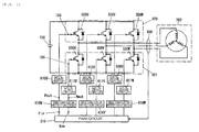
- Fig. 3 is a view for explaining the inverter system according to this embodiment, and shows the constitution of the control part 170 of the inverter device shown in Fig. 2 in more detail.
- the control part 170 includes a PWM circuit 319 in which a CPU, a counter circuit, an input/output circuit and the like are incorporated, gate drive circuits 610U, 610V, 610W, 611U, 611V, 611W for driving IGBTs 328U, 328V, 328W, 330U, 330V, 330W which constitute the above-mentioned switching elements, and simultaneous ON protection circuits 616U, 616V, 616W which calculate signals outputted from the PWM circuit 319 and protect the inverter from short-circuiting.
- the simultaneous ON protection circuits correspond to PWM signal pairs of the upper and lower arms 620, 621 such that the simultaneous ON protection circuit 616U corresponds to the gate drive circuits 610U, 611U, the simultaneous ON protection circuit 616V corresponds to the gate drive circuits 610V, 611V, and the simultaneous ON protection circuit 616W corresponds to the gate drive circuits 610W, 611W.
- the simultaneous ON protection circuit 616U is provided between the PWM circuit 319 and the gate drive circuits 610U, 611U.
- Other simultaneous ON protection circuits 616V, 616W are also arranged in the same manner.
- a current sensor 180 detects electric currents which the IGBTs 328U to 330W constituting switching elements output, and makes the PWM circuit 319 perform a PWM (pulse width modulation) arithmetic operation so as to set the deviation between a predetermined value and a detected current value to zero. Then, a PWM signal (pulse signal) which alternately repeats an ON signal and an OFF signal is outputted to the gate drive circuits 610U to 611W from the PWM circuit 319. Since the gate drive circuits 610U to 611W are constituted by a negative logic, an ON signal assumes a logic "L" level and an OFF signal assumes a logic "H" level.
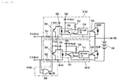
- Fig. 4 is a view showing the circuit constitution of the gate drive circuits 610U, 611U and the simultaneous ON protection circuit 616U.
- the circuit constitution of the V phase and the circuit constitution of the W phase are substantially equal to the circuit constitution of the U phase.
- the gate drive circuit 610U on an upper arm side is constituted of a primary power source 725 (L-Vcc), a secondary power source 726 (H-Vcc1), an input resistor 701, a photocoupler 706, a photocoupler output-use pull-up resistor 727, and a driver IC 710.
- An upper arm switching signal terminal 713 is connected to an input of a primary cathode of the photocoupler 706 via an input resistor 701. Assume a signal inputted to the terminal 713 as Pin.
- An input of the primary anode of the photocoupler 706 is connected to the primary power source 725 (L-Vcc).
- An output of a secondary collector of the photocoupler 706 is connected to the secondary power source 726 via the pull-up resistor 727, and is connected to an input terminal of the driver IC 710. Further, an output of a secondary emitter of the photocoupler 706 is connected to a ground terminal of the driver IC 710.
- An output of the driver IC 710 is connected to a gate electrode terminal 154 of the IGBT 328U.
- the gate drive circuit 611U on a lower arm side is constituted of: a primary power source 725 (L-Vcc), a secondary power source 728 (H-Vcc2), an input resistor 702, a photocoupler 707, a photocoupler-output-use pull-up resistor 729, and a driver IC 711.
- the gate drive circuit 611U substantially has the same constitution as the gate drive circuit 610U.
- a lower arm switching signal terminal 714 is connected to an input of a primary cathode of the photocoupler 707 via an input resistor 702. Assume a signal inputted to the terminal 714 as Nin.
- An input of a primary anode of the photocoupler 707 is connected to a primary power source 725 (L-Vcc), and an output of a secondary collector is connected to a secondary power source 728 (H-Vcc2) via the pull-up resistor 729 and is connected to an input terminal of the driver IC 711.
- An output of a secondary emitter of the photocoupler 707 is connected to a ground terminal of the driver IC 711.
- An output of the driver IC 711 is connected to a gate electrode terminal 164 of the IGBT 330U.
- the simultaneous ON protection circuit 616U is constituted of an OR gate circuit 703 and PNP bipolar transistors 704, 705.
- the upper arm switching signal terminal Pin and the lower arm switching signal terminal Nin are connected to an input of the OR gate circuit 703.
- An output of the OR gate circuit 703 is connected to bases of the PNP bipolar transistors 704, 705.
- a collector and an emitter of the PNP bipolar transistor 704 are connected to an input of a primary cathode and anode of the photocoupler 706 respectively.
- a collector and an emitter of the PNP bipolar transistor 705 are connected to an input of a primary cathode and anode of the photocoupler 707, respectively.
- An upper arm switching signal Pin supplied from the PWM circuit 319 is inputted to an upper arm switching signal terminal 713 of the gate drive circuit 610U.
- a lower arm switching signal Nin supplied from the PWM circuit 319 is inputted to a lower arm switching signal terminal 714 of a gate drive circuit 611U.
- a primary cathode input voltage of the photocoupler 706 becomes equal to a voltage of the primary power source 725 (L-Vcc) via the input resistor 701.
- L-Vcc the primary power source 725
- an output transistor of the photocoupler 706 is also in an OFF state so that an output of the photocoupler 706, that is, an input Pout of the driver IC 710 assumes "H” level by being pulled up by the secondary power source 726 (H-Vcc1).
- the driver IC 710 outputs "L" level to the gate electrode terminal 154 of the IGBT 328U so that the IGBT 328U is turned off.
- the gate drive circuit 611U on a lower arm side also has the same constitution as the gate drive circuit 610U, and a lower arm switching signal is inputted to the lower arm switching signal terminal Nin from the PWM circuit 319.
- a primary cathode input voltage of the photocoupler 707 becomes equal to a voltage of the primary power source 725 (L-Vcc) via the input resistor 702.
- a bias voltage is not applied between a cathode and an anode so that the photo diode is in an OFF state.
- an output transistor of the photocoupler 707 is also in an OFF state so that an input Nout of the driver IC 711 which is an output of the photocoupler 707 assumes "H” level by being pulled up by the secondary power source 728 (H-Vcc2).
- the driver IC 711 outputs "L" level to the gate electrode terminal 164 of the IGBT 330U so that the IGBT 330U is turned off.
- both the IGBTs 328U, 330U of the upper and lower arms are simultaneously turned on so that a power source and a ground are short-circuited whereby a large electric current is generated in the IGBTs 328U, 330U, and the IGBTs 328U, 330U are broken.
- the OR gate circuit 703 outputs "H” level so that the PNP bipolar transistors 704, 705 are turned off. That is, an input PinC of the photocoupler 706 and an input NinC of the photocoupler 707 are not affected so that the gate drive circuits 610U, 611U are operated in accordance with upper arm and lower arm switching signals from the PWM circuit 319.
- a dead time Tdead at gate terminals of the IGBTs 328U, 330U is expressed by a following formula (1).
- Tdead Tdead 319 + TpLH 610 - TpHL 611
- the simultaneous ON protection circuits 616U, 616V, 616W are operated in accordance with a truth-value table shown in Fig. 5 . That is, when a simultaneous ON signal is inputted, the simultaneous ON protection circuits 616U, 616V, 616W forcedly bring input signals supplied to the gate drive circuits 610U to 611W into a logic "H" so that both upper and lower switching elements are turned off whereby short-circuiting of both the upper and lower switching elements is prevented thus protecting the switching elements.
- the simultaneous ON protection circuit 616U in parallel to the gate drive circuits 610U, 611U, as expressed in the formula (1), there is no possibility that the dead time Tdead of the gate electrode terminals 154, 164 of the IGBTs 328U, 330U is affected.
- Fig. 6 shows a comparison example. That is, Fig. 6 shows the circuit constitution of a simultaneous ON protection circuit having substantially the same constitution as the prior art.
- the simultaneous ON protection circuit is constituted of NAND circuits 401 to 404 which calculate signals supplied from the PWM circuit 319. Assume PWM signals which are inputted to the upper arm input terminal 405 and the lower arm input terminal 406 of the simultaneous ON protection circuit as Pin and Nin respectively. In the same manner, assume PWM signals which are outputted from the upper arm output terminal 407 and the lower arm output terminal 408 as Pout and Nout respectively. Also in the case of the simultaneous ON protection circuit 316U shown in Fig. 6 , a truth-value table is expressed by the above-mentioned Fig. 5 .
- the PWM circuit 319 is, for preventing the occurrence of simultaneous turning-on due to irregularities in delay time from the PWM circuit 319 to the gate drive circuits 610U, 611U, provided with a zone where switching is not performed in response to an output signal by delaying ON timing of both upper and lower arm switching elements or advancing OFF timing of both upper and lower arm switching elements. This zone is the above-mentioned dead time Tdead 319.
- the PWM signals inputted to the simultaneous ON protection circuit are, irrelevant of whether or not these signals are a simultaneous ON signal, outputted to the gate drive circuits 610U, 611U via the NAND circuits 401 to 404 in the simultaneous ON protection circuit. Accordingly, timing of signals outputted from the gate drive circuits 610U, 611U are, irrespective of the generation of the simultaneous ON signal, always affected by the simultaneous ON protection circuit so that the difference in delay irregularities (ON/OFF skew) between the upper and lower arms is added to the timing before the signals reach the gate drive circuits 610U, 611U.
- Tdead 2 at the gate electrode terminals 154, 164 of the IGBTs 328U, 330U is expressed by a following formula (2).
- Tdead 319 is a dead time generated by the PWM circuit 319
- TpLH401 is delay time at a point of time that an output of the NAND circuit 401 is changed from “L” ⁇ "H”
- TpHL402 is a delay time at a point of time that an output of the NAND circuit 402 is changed from “H” ⁇ "L”
- TpLH 310 is a delay time at a point of time that an output of the gate drive circuit 610U is changed from “L” ⁇ "H”
- TpHL403 is a delay time at a point of time that an output of the NAND circuit 403 is changed from “H” ⁇ "L”
- TpLH404 is a delay time at a point of time that an output of the NAND circuit 404 is changed from “L” ⁇ "H”
- Tdead Tdead 319 + TpLH ⁇ 401 + TphL ⁇ 402 + TpLH ⁇ 310 - TpLH ⁇ 403 + TphL ⁇ 404 + TpLH ⁇ 311
- the dead time differs between the case where the simultaneous ON protection circuit is provided and the case where the simultaneous ON protection circuit is not provided so that when a PWM signal is transmitted through the simultaneous ON protection circuit, the difference in delay time irregularities Tskew expressed by a following formula (3) is generated.
- Tskew TpLH ⁇ 401 + TphL ⁇ 402 - TpLH ⁇ 403 + TphL ⁇ 404
- Fig. 7 is a timing chart for explaining the manner of operation of the simultaneous ON protection circuit 616U shown in Fig. 4 .
- Pin and Nin indicate signals which are inputted to the upper arm switching signal terminal 713 and the lower arm switching signal terminal 714
- HALTB indicates an output signal of the OR gate circuit 703
- PinC and NinC indicate signals inputted to the photocouplers 706, 707
- Pout and Nout indicate signals inputted to the drivers IC 710, 711
- P-Vg and N-Vg indicate gate signals inputted to gate electrode terminals 154, 164.
- Fig. 7 shows an example where simultaneous ON signals are generated. That is, with respect to the signal Pin inputted to the upper arm switching signal terminal 713, a signal level becomes “H” ⁇ “L” at timing 901 and becomes “L” ⁇ “H” at timing 912. On the other hand, at timing 905 prior to timing 912, a signal Nin of the lower arm switching signal terminal 714 becomes “H” ⁇ "L”. Then, the signal Nin becomes "L” ⁇ "H” at timing 922. Accordingly, during a period between the timing 905 and the timing 912, both signals Pin, Nin assume “L” level so that IBGTs 328U, 330U of the upper and lower arms are simultaneously turned on when the simultaneous ON protection circuit 616U is not provided.
- the input signal PinC of the photocoupler 706 When the signal Pin becomes “H” ⁇ “L” at the timing 901, the input signal PinC of the photocoupler 706 also becomes “H” ⁇ “L” at timing 902. Then, after a lapse of delay time T1 in the photocoupler 706, the input signal Pout of the driver IC 710 becomes “H” ⁇ "L” at timing 903. Thereafter, at timing 904 after a lapse of delay time T2 of the driver IC 710, a signal level of a gate signal P-Vg of the IGBT 328U becomes “L” ⁇ "H” so that the IGBT 328U is turned on.
- time delay (T3+T4) is generated after an input signal NinC of the photocoupler 707 becomes “H” ⁇ “L” at timing 905 and before signals PinC, NinC become “L” ⁇ “H” at timing 909.
- this time delay is approximately 10 to 20ns, even when the simultaneous ON protection circuit 616U is operated, there arises a period where both signals PinC, NinC become “L” level (from the timing 905 to the timing 909) by an amount of this delay time. That is, the simultaneous ON signal remains.
- This simultaneous ON signal is also succeeded by an input signal Pout of the driver IC 710 and an input signal Nout of the driver IC 711, and the input signal Nout of the driver IC 711 which is at "H” level becomes “H” ⁇ “L” at timing 906 after a lapse of delay time T1 in the photocoupler 707 from timing 905 at which the simultaneous ON signal is generated. Then, when the signal NinC becomes “L” ⁇ "H” at timing 909, input signals Pout, Nout of the driver IC 710, 711 become “L” ⁇ "H” at timing 911 after a lapse of the delay time T1 in the photocouplers 706, 707. That is, a hazard (a short pulse between the timing 906 and the timing 911) occurs in the input signal Nout of the driver IC 711.
- a hazard a short pulse between the timing 906 and the timing 911
- a short pulse filter is provided in the inside of a driver IC.
- NPL 1 Infineon Technology, "1ED020112-F Single IGBT Driver IC Datasheet Ver. 2.1", p. 12 paragraph: Input Pulse Suppression IN+, IN-)
- filtering of inputting of a hazard having a pulse width of not more than 30ns is described
- NPL 2 STMicroelectronics, "TD351 Advanced IGBT/MOSFET Driver Data sheet”
- tonmin, p54.1 Input stage filtering of inputting of a hazard having a pulse width of not more than 100ns is described.
- a gate signal P-Vg of the IGBT 328U becomes "H” ⁇ "L” at timing 915 after a lapse of an amount of delay time T2 of the driver IC 710.
- the input signal NinC of the photocoupler 707 becomes “H” ⁇ "L” whereby the input signal Nout of the driver 711 becomes “H” ⁇ "L” at timing 914 after a lapse of an amount of delay time T1 of the photocoupler 707.
- the gate signal N-Vg of the IGBT 330U becomes "L” ⁇ "H” at timing 916 after a lapse of an amount of delay time T2 of the driver IC 711.
- the simultaneous ON protection circuit 616U when a simultaneous ON signal is inputted to the simultaneous ON protection circuit 616U, the simultaneous ON protection circuit 616U interrupts a control signal thus turning off the IBGTs 328U, 330U of the upper and lower arms.
- "H" level is inputted to either one of the upper arm switching signal terminal 713 and the lower arm switching signal terminal 714, that is, when the simultaneous ON signal is not generated, a PWM signal is made to pass through the simultaneous ON protection circuit 616U without being affected by the simultaneous ON protection circuit 616U. Therefore, the simultaneous ON protection circuit 616U does not affect the dead time of upper and lower arms switching signals. Accordingly, the distortion of waveform of the inverter output current can be reduced so that it is possible to provide an inverter which has small rotational irregularities of the motor and large output current amplitude.
- Fig. 8 and Fig. 9 are views for explaining the second embodiment of the invention.
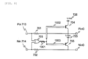
- Fig. 8 is a circuit diagram of a simultaneous ON protection circuit 616U
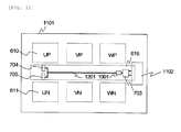
- Fig. 9 is a view showing the layout of wiring of the simultaneous ON protection circuit 616U on a drive circuit board 1101.
- This embodiment is configured such that, as shown in Fig. 8 and Fig. 9 , a series resistor 1001 is inserted into an output of an OR gate circuit 703.
- this embodiment is also applicable to simultaneous ON protection circuits 616V, 610W in substantially the same manner.
- a gate drive circuit is constituted of an upper-arm-use gate drive circuit which includes an upper arm driver IC and a lower-arm-use gate drive circuit which includes a lower arm driver IC, and the upper-arm-use gate drive circuit and the lower-arm-use gate drive circuit are arranged in an electrically insulated manner from each other.
- the upper-arm-use gate drive circuits 610U to 610W are arranged on an upper side of a substrate 1101 in the drawing, and the lower-arm-use gate drive circuits 611U to 611W are arranged on the substrate below the upper-arm-use gate drive circuits 610U to 610W with a space therebetween.
- PNP bipolar transistors 704, 705 of the simultaneous ON protection circuit 616U are arranged at places spaced apart from each other. Accordingly, an output of the OR gate circuit 703 connected to terminals 713, 714 (see Fig. 8 ) of a connector 1102 is wired to the PNP bipolar transistors 704, 705 using bifurcated lines consisting of long lines 1002, 1003.
- the resistor 1001 shown in Fig. 8 and Fig. 9 is inserted into the output of the OR gate circuit 703 as a damping resistor. Due to the provision of the resistor 1001, a voltage change is attenuated in an output of the OR gate circuit 703 so that it is possible to prevent the reflection of signal at the terminal portions of the lines, that is, at bases of the PNP bipolar transistors 704, 705.
- a resistor of 100 ⁇ is used as the resistor 1001.
- the line lengths of the lines 1002, 1003 When line lengths of the lines 1002, 1003 largely differ from each other, ringing is liable to be generated. Accordingly, it is desirable to set the line lengths of the lines 1002, 1003 equal as much as possible. For example, the line lengths of the lines 1002, 1003 can be set equal by routing the shorter line 1003 out of the lines 1002, 1003 in an elongated manner.
- Fig. 10 and Fig. 11 are views showing a modification of the second embodiment.
- Fig. 10 is a circuit diagram of a simultaneous ON protection circuit 616U
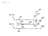
- Fig. 11 is a view showing the layout of wiring of the simultaneous ON protection circuit 616U on a drive circuit board 1101.
- the explanation is made hereinafter by taking the simultaneous ON protection circuit 616U as an example, this embodiment is also applicable to simultaneous ON protection circuits 616V, 610W in substantially the same manner.
- the line is bifurcated into the long lines 1002, 1003 immediately after the resistor 1001, and the long lines 1002, 1003 are connected to the PNP bipolar transistors 704, 705 arranged on an upper side of the respective gate drive circuits 610U, 611U in the drawing.
- the PNP bipolar transistors 704, 705 are arranged in an open space formed between upper-arm-use gate drive circuits 610U to 610W and lower-arm-use gate drive circuits 611U to 611W, and an output of the OR gate circuit 703 and the PNP bipolar transistors 704, 705 are connected to each other via a single long line 1201.
- a resistor 1001 is inserted into an output of the OR gate circuit 703.
- one long line 1201 is used in place of the bifurcated lines consisting of two long lines and hence, the occurrence of ringing can be easily prevented and a wiring space can be made smaller.
- the inverter device includes: the inverter circuit which includes the upper-arm-use IGBTs 328U to 328W and the lower-arm-use IGBTs 330U to 330W; the PWM circuit 319 which outputs a first signal which is an ON/OFF command for the IGBTs 328U to 328W and a second signal which is an ON/OFF command for the IGBTs 330U to 330W; the gate drive circuits 610U to 610W which perform ON/OFF driving of the IGBTs 328U to 328W based on the ON/OFF command which is the first signal; the gate drive circuits 611U to 611W which perform ON/OFF driving of the IGBTs 330U to 330W based on the ON/OFF command which is the second signal; and the simultaneous ON protection circuits 616U to 616W which directly inputs the first signal outputted from the PWM circuit 319 to the gate drive circuits 610U to 610W and directly inputs the
- the simultaneous ON protection circuits 616U to 616W affect the dead time of switching signals of the upper and lower arms.
- each of simultaneous ON protection circuits 616U to 616W may be constituted of PNP bipolar transistors 704, 705 and an OR gate circuit 703 described below.
- the PNP bipolar transistor 704 is provided on an input side of the gate drive circuits 610U to 610W.
- the PNP bipolar transistor 704 inputs a first signal Pin to the gate drive circuits 610U to 610W when the PNP bipolar transistor 704 is turned off, and interrupts inputting of the first signal to the gate drive circuits 610U to 610W and brings an input side of the gate drive circuits 610U to 610W into an OFF command input state when the PNP bipolar transistor 704 is turned on.
- the PNP bipolar transistor 705 is provided on an input side of the gate drive circuits 611U to 611W.
- the PNP bipolar transistor 705 inputs a second signal to the gate drive circuits 611U to 611W when the PNP bipolar transistor 705 is turned off, and interrupts inputting of the second signal into the gate drive circuits 611U to 611W and brings an input side of the gate drive circuits 611U to 611W into an OFF command input state when the PNP bipolar transistor 705 is turned on.
- the OR gate circuit 703 makes the PNP bipolar transistors 704, 705 perform an OFF operation when at least one of the first and second signals is an OFF command, and makes the PNP bipolar transistors 704, 705 perform an ON operation when both first and second signals are ON commands.
- the gate drive circuits 610U to 610W, 611U to 611W respectively include driver ICs 710, 711 for generating a gate voltage, and a short pulse filter time of the driver ICs 710, 711 is set longer than a response time from a point of time that first and second signals in an ON command state are inputted to the OR gate circuit 703 to a point of time that the PNP bipolar transistors 704, 705 are turned on so that the above-mentioned occurrence of hazards in the simultaneous ON protection circuit 616U can be prevented.
Landscapes
- Engineering & Computer Science (AREA)
- Power Engineering (AREA)
- Inverter Devices (AREA)
- General Induction Heating (AREA)
Abstract
Description
- The present invention relates to an inverter device having a circuit for preventing short-circuiting of upper and lower arms of an inverter circuit.
- In an inverter device using a semiconductor switching element, a PWM signal which is a pulse string signal alternately repeating an ON signal and an OFF signal is outputted to respective gate drive circuits for upper and lower arms from a PWM circuit, and both switching elements for upper and lower arms are turned on or off by the gate drive circuit for upper and lower arms.
- Usually, for preventing both switching elements for upper and lower arms from being turned on simultaneously due to irregularities in delay time in outputting a PWM signal from the PWM circuit to the gate drive circuit, a dead time is provided to the PWM circuit for shifting turn-on timing between both switching elements for upper and lower arms. However, there is a case where simultaneous ON signals are outputted by being adversely affected by noises or the like. When the simultaneous ON signals are outputted, a power source and a ground are short-circuited to each other thus giving rise to a drawback that the switching element is broken due to a large electric current which flows at the time of short-circuiting.
- In view of the above, to cope with a case where such a simultaneous ON signal is generated, there has been proposed the constitution where a simultaneous ON protection circuit is provided on a signal path between a PWM circuit and a gate drive circuit (see PTL 1, for example).
- PTL 1:
JP-A-2002-75622 - However, in the constitution described in PTL 1, the simultaneous ON protection circuit is provided between the PWM circuit and the gate drive circuit and hence, a PWM signal outputted from the PWM circuit is inputted to respective gate drive circuits for upper and lower arms via the simultaneous ON protection circuit. Accordingly, ON/OFF timing of a signal outputted from the gate drive circuit is always affected by the simultaneous ON protection circuit regardless of the presence or non-presence of the generation of a simultaneous ON signal. As a result, with respect to a dead time generated by the PWM circuit, at the time that a PWM signal passes through the simultaneous ON protection circuit, due to the influence exerted by the delay time between an input and an output of an element in the simultaneous ON protection circuit, the difference in irregularities in delay time is generated between the upper and lower arms thus giving rise to a drawback that a dead time changes between the upper and lower arms at the time of inputting a signal to the switching element.
- Accordingly, it is necessary to expand a dead time in advance with respect to an output signal of the PWM circuit. However, when the dead time is increased, there arises a drawback that a waveform of an output current from an inverter is distorted so that irregularities in rotation of a motor become large or a drawback that a maximum value of an ON period of the PWM circuit is limited so that amplitude of a maximum output current cannot be increased.
- According to first aspect of the invention, there is provided an inverter device which includes: an inverter circuit which includes an upper-arm-use first switching element and a lower-arm-use second switching element; a control circuit which outputs a first signal which is an ON/OFF command for the first switching element and a second signal which is an ON/OFF command for the second switching element respectively; a first drive circuit which performs ON/OFF driving of the first semiconductor switching element based on the ON/OFF command which is the first signal; a second drive circuit which performs ON/OFF driving of the second semiconductor switching element based on the ON/OFF command which is the second signal; and a signal switching part which directly inputs the first and second signals outputted from the control circuit to the corresponding first and second drive circuits respectively when at least one of the first and second signals is an OFF command, and interrupts inputting of the first signal to the first drive circuit and inputting of the second signal to the second drive circuit and inputs a third signal which is an OFF command to the first and second drive circuits when both the first and second signals are ON commands.
According to a second aspect of the invention, in the inverter device of the first aspect of the invention, the signal switching part may preferably include: a third switching element which switches the interruption and the non-interruption of a first signal path connecting the control circuit and the first drive circuit to each other, and brings the first drive circuit into an OFF command input state when the first signal path is interrupted; a fourth switching element which switches the interruption and the non-interruption of a second signal path connecting the control circuit and the second drive circuit to each other, and brings the second drive circuit into an OFF command input state when the second signal path is interrupted; and a logic circuit which is connected to the first and second signal paths in parallel, outputs an interruption command to the third and fourth switching elements when both the first and second signals are ON commands, and outputs a non-interruption command to the third and fourth switching elements when at least one of the first and second signals is an OFF command.
According to a third aspect of the invention, in the inverter device of the second aspect of the invention, the first and second drive circuits may preferably include a driver IC for generating a gate voltage respectively, and a short pulse filter time of the driver IC is set longer than a response time from a point of time that the first and second signals in an ON command state are inputted to the logic circuit to a point of time that the third and fourth switching elements are brought into an interruption state.
According to a fourth aspect of the invention, in the inverter device of the second or third aspect of the invention, a resistor which prevents the reflection of a signal may preferably be connected in series to a signal output side of the logic circuit. - According to the invention, short-circuiting between the upper and lower arm switching elements can be prevented and, also, a dead time is not affected by a signal which is an ON/OFF command outputted from the control circuit.
-
- [
Fig. 1 ]
A view showing a control block of a hybrid automobile. - [
Fig. 2 ]
A view showing the constitution of aninverter device 140. - [
Fig. 3 ]
A view showing a simultaneous ON protection circuit of theinverter device 140. - [
Fig. 4 ]
A view showing the circuit constitutions ofgate drive circuits ON protection circuit 616U. - [
Fig. 5 ]
A view showing a truth-value table of the simultaneous ON protection circuit. - [
Fig. 6 ]
A block diagram showing the constitution of a simultaneous ON protection circuit in a comparison example. - [
Fig. 7 ]
A timing chart for explaining the manner of operation of the simultaneousON protection circuit 616U. - [
Fig. 8 ]
A view showing the arrangement of aresistor 1001 in the simultaneousON protection circuit 616U. - [
Fig. 9 ]
A view showing the layout of wiring of the simultaneousON protection circuit 616U on adrive circuit board 1101. - [
Fig. 10 ]
A circuit diagram showing a modification of the simultaneousON protection circuit 616U. - [
Fig. 11 ]
A view showing a modification, and a view showing the layout of wiring of the simultaneousON protection circuit 616U on thedrive circuit board 1101. - Hereinafter, the mode for carrying out the invention is explained in conjunction with drawings. An inverter device according to the embodiment of the invention is applicable to a hybrid automobile or a pure electric vehicle. Hereinafter, the explanation is made with respect to a case where the inverter device according to the embodiment of the invention is applied to a hybrid automobile as a typical example. The inverter device according to the embodiment of the invention is explained by taking, as an example, a vehicle-mounted power conversion device of a vehicle-mounted electric machinery system mounted on an automobile, particularly, a vehicle drive inverter device which is used in the vehicle driving electric machinery system and is subject to an extremely severe mounting environment, an extremely severe operation environment or the like.
- The vehicle drive inverter device is provided to a vehicle driving electric machinery system as a control device for controlling driving of a vehicle drive motor, and controls driving of a vehicle drive motor in such a manner that the vehicle drive inverter device converts DC power supplied from a vehicle-mounted battery which constitutes a vehicle-mounted power source or a vehicle-mounted power generator into predetermined AC power, and supplies the obtained AC power to the vehicle drive motor. The vehicle drive motor also has a function of a power generator and hence, the vehicle drive inverter device also has a function of converting AC power generated by the vehicle drive motor into DC power corresponding to an operation mode thereof. The converted DC power is supplied to a vehicle-mounted battery. The constitution of this embodiment is optimally used as the power conversion device for driving a vehicle such as an automobile or a truck.
-
Fig. 1 is a view showing a control block of apower conversion device 200 in a case where the inverter device according to this embodiment of the invention is applied to a hybrid automobile. InFig. 1 , the hybrid electric vehicle (hereinafter described as "HEV") 110 includes two vehicle driving systems. The first vehicle driving system is an engine system where anengine 120 which constitutes an internal combustion engine is used as a power source, and is mainly used as a drive source of the HEV. The second vehicle driving system is a vehicle-mounted electric machinery system wheremotor generators - The
motor generators wheel axle 114 is rotatably and pivotally supported on a front portion of a vehicle body. A pair offront wheels 112 is mounted on both ends of thefront wheel axle 114 respectively. A rear-wheel axle (not shown in the drawing) is rotatably and pivotally supported on a rear portion of the vehicle body. A pair of rear wheels is mounted on both ends of the rear wheel axle respectively. The HEV of this embodiment adopts a so-called front wheel drive system where a main wheel which is driven by power is constituted of thefront wheel 112, and a follower wheel which is rotated due to the rotation of thefront wheel 112 is constituted of the rear wheel. However, it may be possible to adopt a system opposite to the above-mentioned system, that is, a rear wheel drive system. - A front-wheel-side differential gear (hereinafter described as "front-wheel-side DEF") 116 is mounted on a center portion of the
front wheel axle 114. Thefront wheel axle 114 is mechanically connected to an output side of the front-wheel-side DEF 116. An output shaft of atransmission 118 is mechanically connected to an input side of the front-wheel-side DEF 116. The front-wheel-side DEF 116 is a differential power distribution mechanism which distributes a rotational drive force transmitted with a speed changed by thetransmission 118 to left and rightfront wheel axles 114. - An output side of the
motor generator 192 is mechanically connected to an input side of thetransmission 118. An output side of theengine 120 and an output side of themotor generator 194 are mechanically connected to an input side of themotor generator 192 by way of apower distribution mechanism 122. Themotor generators power distribution mechanism 122 are housed in the inside of a housing of thetransmission 118. - The
motor generators motor generators inverter devices power conversion device 200. Abattery 136 is electrically connected to theinverter devices battery 136 and theinverter devices motor generator 192 and theinverter device 140, and a second electrically-operated power generating unit which is constituted of themotor generator 194 and theinverter device 142, and these power generating units are used selectively corresponding to an operation state. - That is, when a vehicle is driven by power from the
engine 120, to assist a drive torque of the vehicle, power is generated using the second electrically-operated power generating unit as the power generating unit by operating the second electrically-operated power generating unit by power from theengine 120, and the first electrically-operated power generating unit is operated as the electrically-operated unit using power obtained by such power generation. Further, in a similar case, to assist a vehicle speed of the vehicle, power is generated using the first electrically-operated power generating unit as the power generating unit by operating the second electrically-operated power generating unit by power of theengine 120, and the second electrically-operated power generating unit is operated as the electrically-operated unit by power obtained by such power generation. - Further, in this embodiment, by operating the first electrically-operated power generating unit as the electrically-operated unit using power of the
battery 136, the vehicle can be driven using only power of themotor generator 192. Further, in this embodiment, power is generated by operating the first electrically-operated power generating unit or the second electrically-operated power generating unit as the power generating unit using power of theengine 120 or power from the wheel, and thebattery 136 is charged with the generated power. - The
battery 136 is also used as a power source for driving themotor 195 used as an accessory. As such an accessory, for example, a motor for driving a compressor of an air conditioner or a motor for driving a hydraulic pump for control is named. DC power is supplied to theinverter device 43 from thebattery 136 and is converted into AC power by theinverter device 43, and the AC power is supplied to themotor 195. - The
inverter device 43 has substantially the same function as theinverter device motor 195. For example, by supplying AC power having a leading phase with respect to the rotation of a rotor of themotor 195, themotor 195 generates a torque. On the other hand, by generating AC power having a lag phase, themotor 195 is operated as a generator so that themotor 195 performs an operation in a regenerative braking state. - The control function of such an
inverter device 43 is substantially equal to the control function of theinverter device motor 195 is smaller than the capacitance of themotor generator inverter device 43 is smaller than the maximum conversion power of theinverter device inverter device 43 is basically equal to the circuit constitution of theinverter device - The
inverter devices inverter device 43 and acapacitor module 500 have the close electrical relationship. Further, these devices have commonality with respect to a point that these devices require a countermeasure to cope with the generation of heat. Still further, there is a demand for the reduction of volumes of these devices as much as possible. In view of the above, the power conversion device described hereinafter houses theinverter devices inverter device 43 and thecapacitor module 500 in the housing thereof. - Due to such a constitution, it is possible to realize the miniaturized device having high reliability. Further, by housing the
inverter devices inverter device 43 and thecapacitor module 500 in one housing, wiring can be effectively simplified and countermeasure against noises can be effectively taken. Further, inductance of a connection circuit between thecapacitor module 500, theinverter devices inverter device 43 can be reduced so that a spike voltage can be reduced, and it is also possible to enhance the reduction of heat generation and the heat radiation efficiency. - Next, the electrical circuit constitution of the
inverter devices inverter device 43 is explained in conjunction withFig. 2 . In the embodiment shown inFig. 1 andFig. 2 , the explanation is made by taking a case where theinverter devices inverter device 43 are respectively individually constituted as an example. Therespective inverter devices inverter device 43 have substantially the same constitution, perform substantially the same operation, and have substantially the same functions and hence, theinverter device 140 is explained hereinafter as a typical example. - The
power conversion device 200 according to this embodiment includes theinverter device 140 and thecapacitor module 500, and theinverter device 140 includes aninverter circuit 144 and acontrol part 170. Thecontrol part 170 includes adriver circuit 174 for controlling driving of theinverter circuit 144, and acontrol circuit 172 which supplies a control signal to thedriver circuit 174 via asignal line 176. - The
inverter circuit 144 is constituted of a three-phase bridge circuit, and includes upper and lower arm series circuits 150 amounting to three phases. The respective upper and lower arm series circuits 150 are electrically connected in parallel between a DCpositive pole terminal 314 and a DCnegative pole terminal 316. The DCpositive pole terminal 314 is electrically connected to a positive pole side of thebattery 136, and a DCnegative pole terminal 316 is electrically connected to a negative pole side of thebattery 136. - The upper and lower arm series circuit 150 includes an IGBT 328 (insulation gate type bipolar transistor) and a
diode 156 which are operated as an upper arm, and anIGBT 330 and adiode 166 which are operated as a lower arm. An intermediate point portion (intermediate electrode 169) of each upper and lower arm series circuit 150 is connected to an AC power line (AC bus bar) 186 which leads to themotor generator 192 via anAC terminal 159. - The
IGBTs control part 170, and convert DC power supplied from thebattery 136 into three-phase AC power. The converted power is supplied to windings of an armature of themotor generator 192. - The
IGBT collector electrode emitter electrode terminal gate electrode terminal 154, 164). As shown in the drawing, thediode collector electrode IGBT diode IGBT IGBT IGBT - An MOSFET (metal oxide semiconductor field effect transistor) may be used as the power semiconductor element for switching. In this case, the
diode 156 and thediode 166 become unnecessary. As described above, upper and lower arm series circuits 150 amounting to three phases are provided corresponding to respective-phase windings of the armature winding of themotor generator 192. In three upper and lower arm series circuits 150, anintermediate electrode 169 which constitutes an intermediate point portion of each arm (that is, a connection portion between the emitter electrode of theIGBT 328 and thecollector electrode 163 of the IGBT 330) is electrically connected to the corresponding phase winding of the armature winding of themotor generator 192 via theAC terminal 159 and theAC connector 188. - The upper and lower arm series circuits 150 are electrically connected in parallel to each other. The
collector electrode 153 of theIGBT 328 of the upper arm is electrically connected to a positive pole side capacitor electrode of thecapacitor module 500 via the positive pole terminal (P terminal) 157 and via a DC bus bar. On the other hand, the emitter electrode of theIGBT 330 of the lower arm is electrically connected to a negative pole side capacitor electrode of thecapacitor module 500 via a negative pole terminal (N terminal) 158 and via the DC bus bar. - The
capacitor module 500 constitutes a smoothing circuit which suppresses the fluctuation of a DC voltage generated by a switching operation of theIGBT battery 136 is electrically connected to the positive pole side capacitor electrode of thecapacitor module 500 via aDC connector 138 and a negative pole side of thebattery 136 is electrically connected to the negative pole side capacitor electrode of thecapacitor module 500 via theDC connector 138. Due to such a constitution, thecapacitor module 500 is connected between thecollector electrode 153 of theupper arm IGBT 328 and the positive pole side of thebattery 136, and is also connected between the emitter electrode of thelower arm IGBT 330 and the negative pole side of thebattery 136 whereby thecapacitor module 500 is electrically connected in parallel to thebattery 136 and the upper and lower arm series circuits 150. - The
control part 170 includes thecontrol circuit 172 and thedriver circuit 174. Thecontrol circuit 172 generates a timing signal for controlling switching timing of theIGBT driver circuit 174 generates a drive signal for making theIGBT control circuit 172. - The
control circuit 172 includes a microcomputer for arithmetically processing switching timing of theIGBT 328, 330 (hereinafter described as "micon") . To the micon, as input information, a target torque value which amotor generator 192 is required to satisfy, a value of an electric current supplied to windings of the armature of themotor generator 192 from upper and lower arm series circuit 150, and magnetic pole positions of the rotor of themotor generator 192 are inputted. The target torque value is based on a command signal outputted from an upper control device not shown in the drawing. The current value is detected based on adetection signal 182 outputted from thecurrent sensor 180. The magnetic pole positions are detected based on a detection signal outputted from a rotation magnetic pole sensor (not shown in the drawing) mounted on themotor generator 192. In this embodiment, the explanation is made by taking the case where a value of an electric current amounting to three phases is detected as an example. However, there is no problem in detecting a value of an electric current amounting to two phases. - The micon in the
control circuit 172 calculates current command values on d and q axes of themotor generator 192 based on a target torque value. Then, voltage command values on d and q axes are calculated based on the differential between the calculated current command values on d and q axes and the detected current values on d and q axes. Further, the calculated voltage command values on d and q axes are converted into voltage command values of a U phase, a V phase and a W phase based on the detected magnetic pole positions. Further, the micon in the inside of thecontrol circuit 172 generates a pulse-shaped modulated wave based on a comparison between a basic wave (sinusoidal wave) based on voltage command values of a U phase, a V phase and a W phase and a carrier wave (triangular wave), and outputs the generated modulated wave to thedriver circuit 174 as a PWM (pulse width modulation) signal. - Here, the
driver circuit 174, to drive the lower arm, amplifies a PWM signal and outputs the amplified PWM signal to the gate electrode of theIGBT 330 of the lower arm as a drive signal. On the other hand, thedriver circuit 174, to drive the upper arm, shifts a level of a reference potential of the PWM signal to a level of a reference potential of the upper arm, amplifies the PWM signal, and outputs the amplified PWM signal to the gate electrode of theIGBT 328 of the upper arm as the drive signal. Due to such a constitution, therespective IGBTs - The
control part 170 protects the upper and lower arm series circuit 150 by performing the detection of abnormality (over-current, over-voltage, over-temperature or the like). For this end, sensing information is inputted to thecontrol part 170. For example, from the signal-useemitter electrode terminals respective IGBTs emitter electrode terminals corresponding IGBT IGBT - Information on a temperature of the upper and lower arm series circuit 150 is inputted to the micon from the temperature sensor (not shown in the drawing) mounted in the upper and lower arm series circuit 150. Further, information on voltage on a DC positive pole side of the upper and lower arm series circuit 150 is inputted to the micon. The micon performs the detection of an over-temperature and the detection of an over-voltage based on these information. When the over-temperature or the over-voltage is detected, the micon completely stops a switching operation of all
IGBTs - An operation of making the
IGBTs inverter circuit 144 conductive and an operation of blocking the upper and lower arms are switched in accordance with a fixed sequence. An electric current in the windings of the armature of themotor generator 192 at the time of switching flows through a circuit constituted of thediodes - The upper and lower arm series circuits 150 include, as shown in the drawing, a positive terminal (P terminal, positive pole terminal) 157, a negative terminal (N terminal, negative pole terminal) 158, an
AC terminal 159 led from anintermediate electrode 169 of the upper and lower arms, a signal-use terminal (signal-use emitter electrode terminal) 155 of the upper arm, thegate electrode terminal 154 of the upper arm, a signal-use terminal (signal-use emitter electrode terminal) 165 of the lower arm, and thegate electrode terminal 164 of the lower arm. - The
power conversion device 200 includes theDC connector 138 on an input side and anAC connector 188 on an output side, and is connected to thebattery 136 and themotor generator 192 via therespective connectors power conversion device 200 may have the circuit constitution where two upper and lower arm series circuits are connected in parallel to each other in each phase. -
Fig. 3 is a view for explaining the inverter system according to this embodiment, and shows the constitution of thecontrol part 170 of the inverter device shown inFig. 2 in more detail. Thecontrol part 170 includes aPWM circuit 319 in which a CPU, a counter circuit, an input/output circuit and the like are incorporated,gate drive circuits IGBTs ON protection circuits PWM circuit 319 and protect the inverter from short-circuiting. - Here, the simultaneous ON protection circuits correspond to PWM signal pairs of the upper and
lower arms ON protection circuit 616U corresponds to thegate drive circuits ON protection circuit 616V corresponds to thegate drive circuits ON protection circuit 616W corresponds to thegate drive circuits 610W, 611W. The simultaneousON protection circuit 616U is provided between thePWM circuit 319 and thegate drive circuits ON protection circuits - In the circuit constitution shown in
Fig. 3 , acurrent sensor 180 detects electric currents which theIGBTs 328U to 330W constituting switching elements output, and makes thePWM circuit 319 perform a PWM (pulse width modulation) arithmetic operation so as to set the deviation between a predetermined value and a detected current value to zero. Then, a PWM signal (pulse signal) which alternately repeats an ON signal and an OFF signal is outputted to thegate drive circuits 610U to 611W from thePWM circuit 319. Since thegate drive circuits 610U to 611W are constituted by a negative logic, an ON signal assumes a logic "L" level and an OFF signal assumes a logic "H" level. -
Fig. 4 is a view showing the circuit constitution of thegate drive circuits ON protection circuit 616U. The circuit constitution of the V phase and the circuit constitution of the W phase are substantially equal to the circuit constitution of the U phase. Thegate drive circuit 610U on an upper arm side is constituted of a primary power source 725 (L-Vcc), a secondary power source 726 (H-Vcc1), aninput resistor 701, aphotocoupler 706, a photocoupler output-use pull-upresistor 727, and adriver IC 710. - An upper arm switching
signal terminal 713 is connected to an input of a primary cathode of thephotocoupler 706 via aninput resistor 701. Assume a signal inputted to the terminal 713 as Pin. An input of the primary anode of thephotocoupler 706 is connected to the primary power source 725 (L-Vcc). An output of a secondary collector of thephotocoupler 706 is connected to thesecondary power source 726 via the pull-upresistor 727, and is connected to an input terminal of thedriver IC 710. Further, an output of a secondary emitter of thephotocoupler 706 is connected to a ground terminal of thedriver IC 710. An output of thedriver IC 710 is connected to agate electrode terminal 154 of theIGBT 328U. - The
gate drive circuit 611U on a lower arm side is constituted of: a primary power source 725 (L-Vcc), a secondary power source 728 (H-Vcc2), aninput resistor 702, aphotocoupler 707, a photocoupler-output-use pull-upresistor 729, and adriver IC 711. Thegate drive circuit 611U substantially has the same constitution as thegate drive circuit 610U. A lower armswitching signal terminal 714 is connected to an input of a primary cathode of thephotocoupler 707 via aninput resistor 702. Assume a signal inputted to the terminal 714 as Nin. An input of a primary anode of thephotocoupler 707 is connected to a primary power source 725 (L-Vcc), and an output of a secondary collector is connected to a secondary power source 728 (H-Vcc2) via the pull-upresistor 729 and is connected to an input terminal of thedriver IC 711. An output of a secondary emitter of thephotocoupler 707 is connected to a ground terminal of thedriver IC 711. An output of thedriver IC 711 is connected to agate electrode terminal 164 of theIGBT 330U. - The simultaneous
ON protection circuit 616U is constituted of anOR gate circuit 703 and PNPbipolar transistors OR gate circuit 703. An output of theOR gate circuit 703 is connected to bases of the PNPbipolar transistors bipolar transistor 704 are connected to an input of a primary cathode and anode of thephotocoupler 706 respectively. A collector and an emitter of the PNPbipolar transistor 705 are connected to an input of a primary cathode and anode of thephotocoupler 707, respectively. - An upper arm switching signal Pin supplied from the
PWM circuit 319 is inputted to an upper arm switchingsignal terminal 713 of thegate drive circuit 610U. On the other hand, a lower arm switching signal Nin supplied from thePWM circuit 319 is inputted to a lower armswitching signal terminal 714 of agate drive circuit 611U. These signals outputted from thePWM circuit 319 are negative logic signals so that "L" level means active. That is, "L" level corresponds to turning-on of theIGBT - Firstly, considered is a case where the upper arm switching
signal terminal 713 is at "H" level. In this case, a primary cathode input voltage of thephotocoupler 706 becomes equal to a voltage of the primary power source 725 (L-Vcc) via theinput resistor 701. As a result, in the photo diode of thephotocoupler 706, a bias voltage is not applied between a cathode and an anode so that the photo diode is in an OFF state. Accordingly, an output transistor of thephotocoupler 706 is also in an OFF state so that an output of thephotocoupler 706, that is, an input Pout of thedriver IC 710 assumes "H" level by being pulled up by the secondary power source 726 (H-Vcc1). Accordingly, thedriver IC 710 outputs "L" level to thegate electrode terminal 154 of theIGBT 328U so that theIGBT 328U is turned off. - Next, considered is a case where "L" level is inputted to the upper arm switching
signal terminal 713. In this case, a primary cathode input voltage of thephotocoupler 706 is lowered via theinput resistor 701 so that a forward bias voltage is applied to a photo diode of thephotocoupler 706 via theinput resistor 701. As a result, an output transistor of thephotocoupler 706 is turned on so that an output of thephotocoupler 706, that is, an input Pout of the driver IC 70 assumes "L" level. Then, the driver IC 70 brings thegate electrode terminal 154 of theIGBT 328U into "H" level so that theIGBT 328U is turned on. - The
gate drive circuit 611U on a lower arm side also has the same constitution as thegate drive circuit 610U, and a lower arm switching signal is inputted to the lower arm switching signal terminal Nin from thePWM circuit 319. - In a case where the lower arm
switching signal terminal 714 is at "H" level, a primary cathode input voltage of thephotocoupler 707 becomes equal to a voltage of the primary power source 725 (L-Vcc) via theinput resistor 702. As a result, in the photo diode of thephotocoupler 707, a bias voltage is not applied between a cathode and an anode so that the photo diode is in an OFF state. Accordingly, an output transistor of thephotocoupler 707 is also in an OFF state so that an input Nout of thedriver IC 711 which is an output of thephotocoupler 707 assumes "H" level by being pulled up by the secondary power source 728 (H-Vcc2). Accordingly, thedriver IC 711 outputs "L" level to thegate electrode terminal 164 of theIGBT 330U so that theIGBT 330U is turned off. - On the other hand, in a case where "L" level is inputted to the lower arm
switching signal terminal 714, a primary cathode input voltage of thephotocoupler 707 is lowered via theinput resistor 702 so that a forward bias voltage is applied to a photo diode of thephotocoupler 707 via theinput resistor 702. As a result, an output transistor of thephotocoupler 707 is turned on so that an input Nout of thedriver IC 711 which is an output of thephotocoupler 707 assumes "L" level. Then, thedriver IC 711 brings thegate electrode terminal 164 of theIGBT 330U into "H" level so that theIGBT 330U is turned on. - Next, the manner of operation of the simultaneous
ON protection circuit 616U is explained. To an input side of theOR gate circuit 703 of the simultaneousON protection circuit 616U, signals Pin, Nin which are inputted to an upper arm switchingsignal terminal 713 and a lower armswitching signal terminal 714 are inputted. Accordingly, when "L" level is simultaneously inputted to both the upper arm switchingsignal terminal 713 and the lower arm switching signal terminal 714 (simultaneous ON signal), theOR gate circuit 703 outputs "L" level, and in other cases (cases where either one of theterminals OR gate circuit 703 outputs "H" level. - When "L" level is simultaneously inputted to both the upper arm switching
signal terminal 713 and the lower armswitching signal terminal 714 so that theOR gate circuit 703 outputs "L" level, the PNPbipolar transistors photocouplers photocouplers - When primary anode-cathode voltages of the
photocouplers photocouplers driver IC 710 and an input Nout to thedriver IC 711 are set at "H" level respectively. As a result, thedriver IC 710 outputs "L" to thegate electrode terminal 154 of theIGBT 328U so that theIGBT 328U is turned off. In the same manner, thedriver IC 711 also outputs "L" to thegate electrode terminal 164 of theIGBT 330U so that theIGBT 330U is turned off. - To consider a case where the simultaneous
ON protection circuit 616U is not provided, when a simultaneous ON signal is inputted to thegate drive circuits IGBTs IGBTs IGBTs ON protection circuit 616U, when such a simultaneous ON signal is generated, "L" level is outputted to theIGBTs IGBTs - On the other hand, when a simultaneous ON signal is not inputted, that is, when "H" level is inputted to either one of the upper arm switching
signal terminal 713 and the lower armswitching signal terminal 714, theOR gate circuit 703 outputs "H" level so that the PNPbipolar transistors photocoupler 706 and an input NinC of thephotocoupler 707 are not affected so that thegate drive circuits PWM circuit 319. - For example, assuming a delay time of output "L" → "H" of the
gate drive circuit 610U asTpLH 610U and a delay time of output "H" → "L" of thegate drive circuit 611U asTpLH 611U, a dead time Tdead at gate terminals of theIGBTs ON protection circuits 
- In this manner, the simultaneous
ON protection circuits Fig. 5 . That is, when a simultaneous ON signal is inputted, the simultaneousON protection circuits gate drive circuits 610U to 611W into a logic "H" so that both upper and lower switching elements are turned off whereby short-circuiting of both the upper and lower switching elements is prevented thus protecting the switching elements. Further, by arranging the simultaneousON protection circuit 616U in parallel to thegate drive circuits gate electrode terminals IGBTs -
Fig. 6 shows a comparison example. That is,Fig. 6 shows the circuit constitution of a simultaneous ON protection circuit having substantially the same constitution as the prior art. The simultaneous ON protection circuit is constituted ofNAND circuits 401 to 404 which calculate signals supplied from thePWM circuit 319. Assume PWM signals which are inputted to the upperarm input terminal 405 and the lowerarm input terminal 406 of the simultaneous ON protection circuit as Pin and Nin respectively. In the same manner, assume PWM signals which are outputted from the upperarm output terminal 407 and the lowerarm output terminal 408 as Pout and Nout respectively. Also in the case of the simultaneous ON protection circuit 316U shown inFig. 6 , a truth-value table is expressed by the above-mentionedFig. 5 . - As described previously, the
PWM circuit 319 is, for preventing the occurrence of simultaneous turning-on due to irregularities in delay time from thePWM circuit 319 to thegate drive circuits dead time Tdead 319. - In the constitution shown in
Fig. 6 , the PWM signals inputted to the simultaneous ON protection circuit are, irrelevant of whether or not these signals are a simultaneous ON signal, outputted to thegate drive circuits NAND circuits 401 to 404 in the simultaneous ON protection circuit. Accordingly, timing of signals outputted from thegate drive circuits gate drive circuits - That is, the dead time Tdead 2 at the
gate electrode terminals IGBTs Tdead 319 is a dead time generated by thePWM circuit 319, TpLH401 is delay time at a point of time that an output of theNAND circuit 401 is changed from "L" → "H", TpHL402 is a delay time at a point of time that an output of theNAND circuit 402 is changed from "H" → "L", TpLH 310 is a delay time at a point of time that an output of thegate drive circuit 610U is changed from "L" → "H", TpHL403 is a delay time at a point of time that an output of theNAND circuit 403 is changed from "H" → "L", TpLH404 is a delay time at a point of time that an output of theNAND circuit 404 is changed from "L" → "H", and TpHL 311 is a delay time at a point of time that an output of thegate drive circuit 611U is changed from "H" → "L".
- Accordingly, in the comparison example shown in
Fig. 6 , the dead time differs between the case where the simultaneous ON protection circuit is provided and the case where the simultaneous ON protection circuit is not provided so that when a PWM signal is transmitted through the simultaneous ON protection circuit, the difference in delay time irregularities Tskew expressed by a following formula (3) is generated.
- On the other hand, according to this embodiment, as described above, when "H" level is inputted to either one of the upper arm switching
signal terminal 713 and the lower armswitching signal terminal 714, that is, a simultaneous ON signal is not generated, a PWM signal passes through the simultaneousON protection circuit 616U without being affected by the simultaneousON protection circuit 616U and is inputted to thegate drive circuits -
Fig. 7 is a timing chart for explaining the manner of operation of the simultaneousON protection circuit 616U shown inFig. 4 . InFig. 7 , Pin and Nin indicate signals which are inputted to the upper arm switchingsignal terminal 713 and the lower armswitching signal terminal 714, HALTB indicates an output signal of theOR gate circuit 703, PinC and NinC indicate signals inputted to thephotocouplers drivers IC gate electrode terminals -
Fig. 7 shows an example where simultaneous ON signals are generated. That is, with respect to the signal Pin inputted to the upper arm switchingsignal terminal 713, a signal level becomes "H" → "L" attiming 901 and becomes "L" → "H" attiming 912. On the other hand, attiming 905 prior totiming 912, a signal Nin of the lower armswitching signal terminal 714 becomes "H" → "L". Then, the signal Nin becomes "L" → "H" attiming 922. Accordingly, during a period between thetiming 905 and thetiming 912, both signals Pin, Nin assume "L" level so thatIBGTs ON protection circuit 616U is not provided. - When the signal Pin becomes "H" → "L" at the
timing 901, the input signal PinC of thephotocoupler 706 also becomes "H" → "L" attiming 902. Then, after a lapse of delay time T1 in thephotocoupler 706, the input signal Pout of thedriver IC 710 becomes "H" → "L" attiming 903. Thereafter, attiming 904 after a lapse of delay time T2 of thedriver IC 710, a signal level of a gate signal P-Vg of theIGBT 328U becomes "L" → "H" so that theIGBT 328U is turned on. - Next, at
timing 905 before the signal Pin inputted to the upperarm switching terminal 713 returns "L" → "H", a signal level of the signal Nin inputted to the lower armswitching signal terminal 714 becomes "H" → "L". Here, an input signal NinC of thephotocoupler 707 readily becomes "H" → "L". Since both signal levels of the signals Pin and Nin assume "L", attiming 908 after a lapse of the delay time T3 of theOR gate circuit 703, an output signal HALTB of theOR gate circuit 703 becomes "H" → "L" so that the PNPbipolar transistors timing 909 after a lapse of a delay time T4 of the PNPbipolar transistors bipolar transistors photocouplers - However, the delay times T3 and T4 are provided in the
OR gate circuit 703 and the PNPbipolar transistors photocoupler 707 becomes "H" → "L" attiming 905 and before signals PinC, NinC become "L" → "H" attiming 909. Although this time delay is approximately 10 to 20ns, even when the simultaneousON protection circuit 616U is operated, there arises a period where both signals PinC, NinC become "L" level (from thetiming 905 to the timing 909) by an amount of this delay time. That is, the simultaneous ON signal remains. - This simultaneous ON signal is also succeeded by an input signal Pout of the
driver IC 710 and an input signal Nout of thedriver IC 711, and the input signal Nout of thedriver IC 711 which is at "H" level becomes "H" → "L" attiming 906 after a lapse of delay time T1 in thephotocoupler 707 from timing 905 at which the simultaneous ON signal is generated. Then, when the signal NinC becomes "L" → "H" attiming 909, input signals Pout, Nout of thedriver IC photocouplers timing 906 and the timing 911) occurs in the input signal Nout of thedriver IC 711. - In this manner, the above-mentioned hazard occurs in the simultaneous
ON protection circuit 616U. However, in general, a short pulse filter is provided in the inside of a driver IC. For example, on a data sheet of a driver IC described in NPL 1 (Infineon Technology, "1ED020112-F Single IGBT Driver IC Datasheet Ver. 2.1", p. 12 paragraph: Input Pulse Suppression IN+, IN-), filtering of inputting of a hazard having a pulse width of not more than 30ns is described, and on a data sheet of a driver IC described in NPL 2 (STMicroelectronics, "TD351 Advanced IGBT/MOSFET Driver Data sheet", p. 4 paragraph: tonmin, p54.1 Input stage), filtering of inputting of a hazard having a pulse width of not more than 100ns is described. - Accordingly, the above-mentioned hazard of short time which appears in the signal Nout is filtered by the
driver IC 711 so that, as indicated by a dottedline 907 indicative of a signal N-Vg, the hazard is not outputted to thegate electrode terminal 164 of theIGBT 330U whereby the short-circuiting of the upper and lower arms is avoided. On the other hand, with respect to the upper arm, a gate signal P-Vg of theIGBT 328U becomes "H" → "L" attiming 915 after a lapse of an amount of delay time T2 of thedriver IC 710. - Next, when the signal Pin of the upper
arm switching terminal 713 becomes "L" → "H" attiming 912, the simultaneous ON signal state is finished. As a result, attiming 921 after a lapse of delay time T3 of theOR gate circuit 703, the output signal HALTB of theOR gate circuit 703 becomes "L" → "H", and attiming 913 after a lapse of delay time T4 of the PNPbipolar transistors bipolar transistors arm switching terminal 714 is "L", the input signal NinC of thephotocoupler 707 becomes "H" → "L" whereby the input signal Nout of thedriver 711 becomes "H" → "L" attiming 914 after a lapse of an amount of delay time T1 of thephotocoupler 707. Then, the gate signal N-Vg of theIGBT 330U becomes "L" → "H" attiming 916 after a lapse of an amount of delay time T2 of thedriver IC 711. - Thereafter, when the signal Nin of the lower
arm switching terminal 714 becomes "L" → "H" attiming 922, the input signal NinC of thephotocoupler 707 becomes "L" → "H" and, further, at timing 923 after a lapse of an amount of delay time T1 of thephotocoupler 707, the input signal Nout of thedriver 711 becomes "L" → "H". Then, attiming 924 after a lapse of an amount of delay time T2 of thedriver IC 711, the gate signal N-Vg of theIGBT 330U becomes "H" → "L". - In this manner, with respect to the simultaneous
ON protection circuit 616U of the invention, when a simultaneous ON signal is inputted to the simultaneousON protection circuit 616U, the simultaneousON protection circuit 616U interrupts a control signal thus turning off theIBGTs signal terminal 713 and the lower armswitching signal terminal 714, that is, when the simultaneous ON signal is not generated, a PWM signal is made to pass through the simultaneousON protection circuit 616U without being affected by the simultaneousON protection circuit 616U. Therefore, the simultaneousON protection circuit 616U does not affect the dead time of upper and lower arms switching signals. Accordingly, the distortion of waveform of the inverter output current can be reduced so that it is possible to provide an inverter which has small rotational irregularities of the motor and large output current amplitude. -
Fig. 8 andFig. 9 are views for explaining the second embodiment of the invention.Fig. 8 is a circuit diagram of a simultaneousON protection circuit 616U, andFig. 9 is a view showing the layout of wiring of the simultaneousON protection circuit 616U on adrive circuit board 1101. This embodiment is configured such that, as shown inFig. 8 andFig. 9 , aseries resistor 1001 is inserted into an output of anOR gate circuit 703. Although the explanation is made hereinafter by taking the simultaneousON protection circuit 616U as an example, this embodiment is also applicable to simultaneousON protection circuits 616V, 610W in substantially the same manner. - In general, a gate drive circuit is constituted of an upper-arm-use gate drive circuit which includes an upper arm driver IC and a lower-arm-use gate drive circuit which includes a lower arm driver IC, and the upper-arm-use gate drive circuit and the lower-arm-use gate drive circuit are arranged in an electrically insulated manner from each other. In the layout shown in
Fig. 9 , the upper-arm-usegate drive circuits 610U to 610W are arranged on an upper side of asubstrate 1101 in the drawing, and the lower-arm-usegate drive circuits 611U to 611W are arranged on the substrate below the upper-arm-usegate drive circuits 610U to 610W with a space therebetween. In such an arrangement, PNPbipolar transistors ON protection circuit 616U are arranged at places spaced apart from each other. Accordingly, an output of theOR gate circuit 703 connected toterminals 713, 714 (seeFig. 8 ) of aconnector 1102 is wired to the PNPbipolar transistors long lines - In the simultaneous
ON protection circuit 616U shown inFig. 4 , when an IC is used as theOR gate circuit 703, an output signal voltage of theOR gate circuit 703 steeply changes. When such a steeply changing voltage is inputted to thelong lines Fig. 9 , the lines exhibit the behavior of a distributed constant circuit. Accordingly, unless processing such as impedance matching is taken at terminal portions of the lines, the reflection occurs thus giving rise to overshooting of a signal voltage. Further, in a case where the lines are provided in a bifurcated manner, when lengths of the lines are imbalanced, ringing is liable to occur due to reciprocation of a reflection signal. Such overshooting of the signal voltage and ringing may cause an erroneous operation of the circuit, breaking of a semiconductor part and the like. On the other hand, when a resistor for impedance matching is provided to the terminal portions of the lines, there arises a drawback that a signal level is lowered or the power consumption is increased. - Accordingly, in this embodiment, the
resistor 1001 shown inFig. 8 andFig. 9 is inserted into the output of theOR gate circuit 703 as a damping resistor. Due to the provision of theresistor 1001, a voltage change is attenuated in an output of theOR gate circuit 703 so that it is possible to prevent the reflection of signal at the terminal portions of the lines, that is, at bases of the PNPbipolar transistors resistor 1001. - When line lengths of the
lines lines lines shorter line 1003 out of thelines -
Fig. 10 andFig. 11 are views showing a modification of the second embodiment.Fig. 10 is a circuit diagram of a simultaneousON protection circuit 616U, andFig. 11 is a view showing the layout of wiring of the simultaneousON protection circuit 616U on adrive circuit board 1101. Although the explanation is made hereinafter by taking the simultaneousON protection circuit 616U as an example, this embodiment is also applicable to simultaneousON protection circuits 616V, 610W in substantially the same manner. - In the embodiment shown in
Fig. 8 andFig. 9 , the line is bifurcated into thelong lines resistor 1001, and thelong lines bipolar transistors gate drive circuits Fig. 10 andFig. 11 , the PNPbipolar transistors gate drive circuits 610U to 610W and lower-arm-usegate drive circuits 611U to 611W, and an output of theOR gate circuit 703 and the PNPbipolar transistors long line 1201. In the same manner as the above-mentioned embodiment, aresistor 1001 is inserted into an output of theOR gate circuit 703. - In the modification shown in
Fig. 10 andFig. 11 , onelong line 1201 is used in place of the bifurcated lines consisting of two long lines and hence, the occurrence of ringing can be easily prevented and a wiring space can be made smaller. - In this manner, even when the PNP
bipolar transistors - As described above, the inverter device according to this embodiment includes: the inverter circuit which includes the upper-arm-use IGBTs 328U to 328W and the lower-arm-use IGBTs 330U to 330W; the PWM circuit 319 which outputs a first signal which is an ON/OFF command for the IGBTs 328U to 328W and a second signal which is an ON/OFF command for the IGBTs 330U to 330W; the gate drive circuits 610U to 610W which perform ON/OFF driving of the IGBTs 328U to 328W based on the ON/OFF command which is the first signal; the gate drive circuits 611U to 611W which perform ON/OFF driving of the IGBTs 330U to 330W based on the ON/OFF command which is the second signal; and the simultaneous ON protection circuits 616U to 616W which directly inputs the first signal outputted from the PWM circuit 319 to the gate drive circuits 610U to 610W and directly inputs the second signal outputted from the PWM circuit 319 to the gate drive circuits 611U to 611W when at least one of the first and second signals is an OFF command, and interrupts inputting of the first signal to the gate drive circuits 610U to 610W and inputting of the second signal to the gate drive circuits 611U to 611W and inputs a third signal which is an OFF command to the gate drive circuits 610U to 610W and the gate drive circuits 611U to 611W when both the first and second signals are ON commands.
- As a result, when the simultaneous ON signal is generated, the IGBTs of the upper and lower arms are turned off so that short-circuiting of the upper and lower arms can be prevented. Further, when at least one of the first and second signals is an OFF command, that is, when a simultaneous ON signal is not generated, there is no possibility that the simultaneous
ON protection circuits 616U to 616W affect the dead time of switching signals of the upper and lower arms. - For example, each of simultaneous
ON protection circuits 616U to 616W may be constituted of PNPbipolar transistors OR gate circuit 703 described below. The PNPbipolar transistor 704 is provided on an input side of thegate drive circuits 610U to 610W. The PNPbipolar transistor 704 inputs a first signal Pin to thegate drive circuits 610U to 610W when the PNPbipolar transistor 704 is turned off, and interrupts inputting of the first signal to thegate drive circuits 610U to 610W and brings an input side of thegate drive circuits 610U to 610W into an OFF command input state when the PNPbipolar transistor 704 is turned on. On the other hand, the PNPbipolar transistor 705 is provided on an input side of thegate drive circuits 611U to 611W. The PNPbipolar transistor 705 inputs a second signal to thegate drive circuits 611U to 611W when the PNPbipolar transistor 705 is turned off, and interrupts inputting of the second signal into thegate drive circuits 611U to 611W and brings an input side of thegate drive circuits 611U to 611W into an OFF command input state when the PNPbipolar transistor 705 is turned on.
Further, theOR gate circuit 703 makes the PNPbipolar transistors bipolar transistors - Further, the
gate drive circuits 610U to 610W, 611U to 611W respectively includedriver ICs driver ICs OR gate circuit 703 to a point of time that the PNPbipolar transistors ON protection circuit 616U can be prevented. - The above-mentioned embodiments may be used in a single form or in combination because advantageous effects of the respective embodiments can be acquired singly or synergistically. Further, unless the technical features of the invention are not damaged, the invention is not limited to the above-mentioned embodiments in any way.
- Although various embodiments and modifications have been explained heretofore, the invention is not limited to these contents. Other embodiments which are conceivable within the technical concept of the invention also fall within the scope of the invention.
- The content of the disclosure of the following basic application from which the present application claim priority is incorporated in this specification in the form of cited document.
Japanese Patent Application2010-085099 (filed on April 1, 2010
Claims (4)
- An inverter device comprising:an inverter circuit which includes an upper-arm-use first switching element and a lower-arm-use second switching element;a control circuit which outputs a first signal which is an ON/OFF command for the first switching element and a second signal which is an ON/OFF command for the second switching element respectively;a first drive circuit which performs ON/OFF driving of the first semiconductor switching element based on the ON/OFF command which is the first signal;a second drive circuit which performs ON/OFF driving of the second semiconductor switching element based on the ON/OFF command which is the second signal; anda signal switching part which directly inputs the first and second signals outputted from the control circuit to the corresponding first and second drive circuits respectively when at least one of the first and second signals is an OFF command, and interrupts inputting of the first signal to the first drive circuit and inputting of the second signal to the second drive circuit and inputs a third signal which is an OFF command to the first and second drive circuits when both the first and second signals are ON commands.
- The inverter device according to claim 1, wherein the signal switching part comprises:a third switching element which switches the interruption and the non-interruption of a first signal path connecting the control circuit and the first drive circuit to each other, and brings the first drive circuit into an OFF command input state when the first signal path is interrupted;a fourth switching element which switches the interruption and the non-interruption of a second signal path connecting the control circuit and the second drive circuit to each other, and brings the second drive circuit into an OFF command input state when the second signal path is interrupted; anda logic circuit which is connected to the first and second signal paths in parallel, outputs an interruption command to the third and fourth switching elements when both the first and second signals are ON commands, and outputs a non-interruption command to the third and fourth switching elements when at least one of the first and second signals is an OFF command.
- The inverter device according to claim 2, wherein the first and second drive circuits include a driver IC for generating a gate voltage respectively, and
a short pulse filter time of the driver IC is set longer than a response time from a point of time that the first and second signals in an ON command state are inputted to the logic circuit to a point of time that the third and fourth switching elements are brought into an interruption state. - The inverter device according to one of claim 2 to 3, wherein a resistor which prevents the reflection of a signal is connected in series to a signal output side of the logic circuit.
Applications Claiming Priority (2)
| Application Number | Priority Date | Filing Date | Title |
|---|---|---|---|
| JP2010085099A JP5439260B2 (en) | 2010-04-01 | 2010-04-01 | Inverter device |
| PCT/JP2011/058272 WO2011125863A1 (en) | 2010-04-01 | 2011-03-31 | Inverter device |
Publications (3)
| Publication Number | Publication Date |
|---|---|
| EP2555410A1 true EP2555410A1 (en) | 2013-02-06 |
| EP2555410A4 EP2555410A4 (en) | 2018-01-03 |
| EP2555410B1 EP2555410B1 (en) | 2019-05-22 |
Family
ID=44762801
Family Applications (1)
| Application Number | Title | Priority Date | Filing Date |
|---|---|---|---|
| EP11765763.5A Active EP2555410B1 (en) | 2010-04-01 | 2011-03-31 | Inverter device |
Country Status (5)
| Country | Link |
|---|---|
| US (1) | US8971079B2 (en) |
| EP (1) | EP2555410B1 (en) |
| JP (1) | JP5439260B2 (en) |
| CN (1) | CN102835015B (en) |
| WO (1) | WO2011125863A1 (en) |
Families Citing this family (9)
| Publication number | Priority date | Publication date | Assignee | Title |
|---|---|---|---|---|
| KR101983134B1 (en) * | 2012-12-20 | 2019-05-28 | 삼성전기주식회사 | Protection apparatus for inverter |
| JP6252905B2 (en) * | 2013-06-07 | 2017-12-27 | パナソニックIpマネジメント株式会社 | Induction heating device |
| CN104901575B (en) * | 2014-03-05 | 2018-05-25 | 株式会社东芝 | Control device for inverter, power-converting device and vehicle |
| WO2016021329A1 (en) * | 2014-08-04 | 2016-02-11 | 日立オートモティブシステムズ株式会社 | Power conversion device |
| KR102120118B1 (en) * | 2016-08-18 | 2020-06-08 | 주식회사 엘지화학 | Battery module |
| JP6389945B1 (en) * | 2017-11-01 | 2018-09-12 | 高周波熱錬株式会社 | Load abnormality detection circuit for inverter |
| JP6770559B2 (en) * | 2018-08-29 | 2020-10-14 | 株式会社Subaru | Power converters and vehicles |
| JP2024143661A (en) * | 2023-03-30 | 2024-10-11 | 高周波熱錬株式会社 | Dual frequency power supply device, high frequency heating device and high frequency hardening device |
| WO2026028342A1 (en) * | 2024-07-31 | 2026-02-05 | 三菱電機ビルソリューションズ株式会社 | Elevator control device |
Family Cites Families (8)
| Publication number | Priority date | Publication date | Assignee | Title |
|---|---|---|---|---|
| KR910000543B1 (en) * | 1987-03-24 | 1991-01-26 | 자이당호오징 한도오다이 겡큐 싱고오가이 | PWM power converter |
| DE4300981A1 (en) * | 1993-01-15 | 1994-07-21 | Siemens Ag | Control device |
| JP3625692B2 (en) * | 1999-05-28 | 2005-03-02 | 三菱電機株式会社 | Automotive power converter |
| JP3588301B2 (en) * | 2000-03-09 | 2004-11-10 | 三洋電機株式会社 | Half-bridge type inverter circuit |
| JP2002075622A (en) * | 2000-09-04 | 2002-03-15 | Fuji Electric Co Ltd | Electromagnetic cooker power supply |
| JP4880828B2 (en) * | 2001-06-19 | 2012-02-22 | 株式会社東芝 | Inverter device |
| JP4962715B2 (en) * | 2007-03-27 | 2012-06-27 | 日本電気株式会社 | Termination resistance adjustment method and termination resistance adjustment circuit |
| JP2010085099A (en) | 2008-09-29 | 2010-04-15 | Bridgestone Corp | Device and method for monitoring deterioration of antivibration rubber |
-
2010
- 2010-04-01 JP JP2010085099A patent/JP5439260B2/en active Active
-
2011
- 2011-03-31 US US13/638,287 patent/US8971079B2/en active Active
- 2011-03-31 WO PCT/JP2011/058272 patent/WO2011125863A1/en not_active Ceased
- 2011-03-31 EP EP11765763.5A patent/EP2555410B1/en active Active
- 2011-03-31 CN CN201180017432.8A patent/CN102835015B/en active Active
Non-Patent Citations (1)
| Title |
|---|
| See references of WO2011125863A1 * |
Also Published As
| Publication number | Publication date |
|---|---|
| US8971079B2 (en) | 2015-03-03 |
| CN102835015B (en) | 2015-07-29 |
| JP2011217558A (en) | 2011-10-27 |
| EP2555410A4 (en) | 2018-01-03 |
| CN102835015A (en) | 2012-12-19 |
| US20130051099A1 (en) | 2013-02-28 |
| JP5439260B2 (en) | 2014-03-12 |
| WO2011125863A1 (en) | 2011-10-13 |
| EP2555410B1 (en) | 2019-05-22 |
Similar Documents
| Publication | Publication Date | Title |
|---|---|---|
| EP2555410B1 (en) | Inverter device | |
| JP5315155B2 (en) | Semiconductor element control device, automotive electrical system | |
| US9667169B2 (en) | Power conversion apparatus | |
| JP5244653B2 (en) | Power converter | |
| US9166499B2 (en) | Electronic circuit operating based on isolated switching power source | |
| US11114949B2 (en) | Inverter control board that is configured so that a detection circuit is appropriately arranged | |
| EP3651341B1 (en) | Driving power supply device | |
| EP2876809B1 (en) | Electric power converter | |
| CN104682816A (en) | Rotating electric machine driver and electric power steering device | |
| JP6218169B2 (en) | Protection circuit, inverter device | |
| JP4670833B2 (en) | Motor drive device for vehicle | |
| US10790730B2 (en) | Power conversion device | |
| WO2018037720A1 (en) | Power conversion device | |
| JP2016086491A (en) | Semiconductor device | |
| KR20120134434A (en) | Over voltage protection circuit and mdps ecu having the circuit |
Legal Events
| Date | Code | Title | Description |
|---|---|---|---|
| PUAI | Public reference made under article 153(3) epc to a published international application that has entered the european phase |
Free format text: ORIGINAL CODE: 0009012 |
|
| 17P | Request for examination filed |
Effective date: 20121102 |
|
| AK | Designated contracting states |
Kind code of ref document: A1 Designated state(s): AL AT BE BG CH CY CZ DE DK EE ES FI FR GB GR HR HU IE IS IT LI LT LU LV MC MK MT NL NO PL PT RO RS SE SI SK SM TR |
|
| RIN1 | Information on inventor provided before grant (corrected) |
Inventor name: YAHATA, KOICHI Inventor name: SHIMANO, HIROKI Inventor name: TATEYAMA, TETSURO Inventor name: FUNABA, SEIJI Inventor name: NOTO, YASUO |
|
| DAX | Request for extension of the european patent (deleted) | ||
| RA4 | Supplementary search report drawn up and despatched (corrected) |
Effective date: 20171130 |
|
| RIC1 | Information provided on ipc code assigned before grant |
Ipc: H05B 6/06 20060101ALI20171124BHEP Ipc: H02M 7/48 20070101AFI20171124BHEP Ipc: H02M 7/5387 20070101ALI20171124BHEP Ipc: H05B 6/04 20060101ALI20171124BHEP |
|
| REG | Reference to a national code |
Ref country code: DE Ref legal event code: R079 Ref document number: 602011059207 Country of ref document: DE Free format text: PREVIOUS MAIN CLASS: H02M0007480000 Ipc: H02M0007797000 |
|
| GRAP | Despatch of communication of intention to grant a patent |
Free format text: ORIGINAL CODE: EPIDOSNIGR1 |
|
| STAA | Information on the status of an ep patent application or granted ep patent |
Free format text: STATUS: GRANT OF PATENT IS INTENDED |
|
| RIC1 | Information provided on ipc code assigned before grant |
Ipc: H02M 7/797 20060101AFI20190116BHEP |
|
| INTG | Intention to grant announced |
Effective date: 20190204 |
|
| GRAS | Grant fee paid |
Free format text: ORIGINAL CODE: EPIDOSNIGR3 |
|
| GRAA | (expected) grant |
Free format text: ORIGINAL CODE: 0009210 |
|
| STAA | Information on the status of an ep patent application or granted ep patent |
Free format text: STATUS: THE PATENT HAS BEEN GRANTED |
|
| RIN1 | Information on inventor provided before grant (corrected) |
Inventor name: TATEYAMA, TETSURO Inventor name: YAHATA, KOICHI Inventor name: NOTO, YASUO Inventor name: SHIMANO, HIROKI Inventor name: FUNABA, SEIJI |
|
| AK | Designated contracting states |
Kind code of ref document: B1 Designated state(s): AL AT BE BG CH CY CZ DE DK EE ES FI FR GB GR HR HU IE IS IT LI LT LU LV MC MK MT NL NO PL PT RO RS SE SI SK SM TR |
|
| REG | Reference to a national code |
Ref country code: GB Ref legal event code: FG4D |
|
| REG | Reference to a national code |
Ref country code: CH Ref legal event code: EP |
|
| REG | Reference to a national code |
Ref country code: IE Ref legal event code: FG4D |
|
| REG | Reference to a national code |
Ref country code: DE Ref legal event code: R096 Ref document number: 602011059207 Country of ref document: DE |
|
| REG | Reference to a national code |
Ref country code: AT Ref legal event code: REF Ref document number: 1137294 Country of ref document: AT Kind code of ref document: T Effective date: 20190615 |
|
| REG | Reference to a national code |
Ref country code: NL Ref legal event code: MP Effective date: 20190522 |
|
| REG | Reference to a national code |
Ref country code: LT Ref legal event code: MG4D |
|
| PG25 | Lapsed in a contracting state [announced via postgrant information from national office to epo] |
Ref country code: AL Free format text: LAPSE BECAUSE OF FAILURE TO SUBMIT A TRANSLATION OF THE DESCRIPTION OR TO PAY THE FEE WITHIN THE PRESCRIBED TIME-LIMIT Effective date: 20190522 Ref country code: ES Free format text: LAPSE BECAUSE OF FAILURE TO SUBMIT A TRANSLATION OF THE DESCRIPTION OR TO PAY THE FEE WITHIN THE PRESCRIBED TIME-LIMIT Effective date: 20190522 Ref country code: HR Free format text: LAPSE BECAUSE OF FAILURE TO SUBMIT A TRANSLATION OF THE DESCRIPTION OR TO PAY THE FEE WITHIN THE PRESCRIBED TIME-LIMIT Effective date: 20190522 Ref country code: NO Free format text: LAPSE BECAUSE OF FAILURE TO SUBMIT A TRANSLATION OF THE DESCRIPTION OR TO PAY THE FEE WITHIN THE PRESCRIBED TIME-LIMIT Effective date: 20190822 Ref country code: PT Free format text: LAPSE BECAUSE OF FAILURE TO SUBMIT A TRANSLATION OF THE DESCRIPTION OR TO PAY THE FEE WITHIN THE PRESCRIBED TIME-LIMIT Effective date: 20190922 Ref country code: SE Free format text: LAPSE BECAUSE OF FAILURE TO SUBMIT A TRANSLATION OF THE DESCRIPTION OR TO PAY THE FEE WITHIN THE PRESCRIBED TIME-LIMIT Effective date: 20190522 Ref country code: FI Free format text: LAPSE BECAUSE OF FAILURE TO SUBMIT A TRANSLATION OF THE DESCRIPTION OR TO PAY THE FEE WITHIN THE PRESCRIBED TIME-LIMIT Effective date: 20190522 Ref country code: LT Free format text: LAPSE BECAUSE OF FAILURE TO SUBMIT A TRANSLATION OF THE DESCRIPTION OR TO PAY THE FEE WITHIN THE PRESCRIBED TIME-LIMIT Effective date: 20190522 Ref country code: NL Free format text: LAPSE BECAUSE OF FAILURE TO SUBMIT A TRANSLATION OF THE DESCRIPTION OR TO PAY THE FEE WITHIN THE PRESCRIBED TIME-LIMIT Effective date: 20190522 |
|
| PG25 | Lapsed in a contracting state [announced via postgrant information from national office to epo] |
Ref country code: RS Free format text: LAPSE BECAUSE OF FAILURE TO SUBMIT A TRANSLATION OF THE DESCRIPTION OR TO PAY THE FEE WITHIN THE PRESCRIBED TIME-LIMIT Effective date: 20190522 Ref country code: LV Free format text: LAPSE BECAUSE OF FAILURE TO SUBMIT A TRANSLATION OF THE DESCRIPTION OR TO PAY THE FEE WITHIN THE PRESCRIBED TIME-LIMIT Effective date: 20190522 Ref country code: BG Free format text: LAPSE BECAUSE OF FAILURE TO SUBMIT A TRANSLATION OF THE DESCRIPTION OR TO PAY THE FEE WITHIN THE PRESCRIBED TIME-LIMIT Effective date: 20190822 Ref country code: GR Free format text: LAPSE BECAUSE OF FAILURE TO SUBMIT A TRANSLATION OF THE DESCRIPTION OR TO PAY THE FEE WITHIN THE PRESCRIBED TIME-LIMIT Effective date: 20190823 |
|
| REG | Reference to a national code |
Ref country code: AT Ref legal event code: MK05 Ref document number: 1137294 Country of ref document: AT Kind code of ref document: T Effective date: 20190522 |
|
| PG25 | Lapsed in a contracting state [announced via postgrant information from national office to epo] |
Ref country code: AT Free format text: LAPSE BECAUSE OF FAILURE TO SUBMIT A TRANSLATION OF THE DESCRIPTION OR TO PAY THE FEE WITHIN THE PRESCRIBED TIME-LIMIT Effective date: 20190522 Ref country code: DK Free format text: LAPSE BECAUSE OF FAILURE TO SUBMIT A TRANSLATION OF THE DESCRIPTION OR TO PAY THE FEE WITHIN THE PRESCRIBED TIME-LIMIT Effective date: 20190522 Ref country code: SK Free format text: LAPSE BECAUSE OF FAILURE TO SUBMIT A TRANSLATION OF THE DESCRIPTION OR TO PAY THE FEE WITHIN THE PRESCRIBED TIME-LIMIT Effective date: 20190522 Ref country code: EE Free format text: LAPSE BECAUSE OF FAILURE TO SUBMIT A TRANSLATION OF THE DESCRIPTION OR TO PAY THE FEE WITHIN THE PRESCRIBED TIME-LIMIT Effective date: 20190522 Ref country code: CZ Free format text: LAPSE BECAUSE OF FAILURE TO SUBMIT A TRANSLATION OF THE DESCRIPTION OR TO PAY THE FEE WITHIN THE PRESCRIBED TIME-LIMIT Effective date: 20190522 Ref country code: RO Free format text: LAPSE BECAUSE OF FAILURE TO SUBMIT A TRANSLATION OF THE DESCRIPTION OR TO PAY THE FEE WITHIN THE PRESCRIBED TIME-LIMIT Effective date: 20190522 |
|
| REG | Reference to a national code |
Ref country code: DE Ref legal event code: R097 Ref document number: 602011059207 Country of ref document: DE |
|
| PG25 | Lapsed in a contracting state [announced via postgrant information from national office to epo] |
Ref country code: SM Free format text: LAPSE BECAUSE OF FAILURE TO SUBMIT A TRANSLATION OF THE DESCRIPTION OR TO PAY THE FEE WITHIN THE PRESCRIBED TIME-LIMIT Effective date: 20190522 Ref country code: IT Free format text: LAPSE BECAUSE OF FAILURE TO SUBMIT A TRANSLATION OF THE DESCRIPTION OR TO PAY THE FEE WITHIN THE PRESCRIBED TIME-LIMIT Effective date: 20190522 |
|
| PLBE | No opposition filed within time limit |
Free format text: ORIGINAL CODE: 0009261 |
|
| STAA | Information on the status of an ep patent application or granted ep patent |
Free format text: STATUS: NO OPPOSITION FILED WITHIN TIME LIMIT |
|
| PG25 | Lapsed in a contracting state [announced via postgrant information from national office to epo] |
Ref country code: TR Free format text: LAPSE BECAUSE OF FAILURE TO SUBMIT A TRANSLATION OF THE DESCRIPTION OR TO PAY THE FEE WITHIN THE PRESCRIBED TIME-LIMIT Effective date: 20190522 |
|
| 26N | No opposition filed |
Effective date: 20200225 |
|
| PG25 | Lapsed in a contracting state [announced via postgrant information from national office to epo] |
Ref country code: PL Free format text: LAPSE BECAUSE OF FAILURE TO SUBMIT A TRANSLATION OF THE DESCRIPTION OR TO PAY THE FEE WITHIN THE PRESCRIBED TIME-LIMIT Effective date: 20190522 |
|
| PG25 | Lapsed in a contracting state [announced via postgrant information from national office to epo] |
Ref country code: SI Free format text: LAPSE BECAUSE OF FAILURE TO SUBMIT A TRANSLATION OF THE DESCRIPTION OR TO PAY THE FEE WITHIN THE PRESCRIBED TIME-LIMIT Effective date: 20190522 |
|
| PG25 | Lapsed in a contracting state [announced via postgrant information from national office to epo] |
Ref country code: MC Free format text: LAPSE BECAUSE OF FAILURE TO SUBMIT A TRANSLATION OF THE DESCRIPTION OR TO PAY THE FEE WITHIN THE PRESCRIBED TIME-LIMIT Effective date: 20190522 |
|
| REG | Reference to a national code |
Ref country code: CH Ref legal event code: PL |
|
| REG | Reference to a national code |
Ref country code: BE Ref legal event code: MM Effective date: 20200331 |
|
| PG25 | Lapsed in a contracting state [announced via postgrant information from national office to epo] |
Ref country code: LU Free format text: LAPSE BECAUSE OF NON-PAYMENT OF DUE FEES Effective date: 20200331 |
|
| PG25 | Lapsed in a contracting state [announced via postgrant information from national office to epo] |
Ref country code: IE Free format text: LAPSE BECAUSE OF NON-PAYMENT OF DUE FEES Effective date: 20200331 Ref country code: CH Free format text: LAPSE BECAUSE OF NON-PAYMENT OF DUE FEES Effective date: 20200331 Ref country code: LI Free format text: LAPSE BECAUSE OF NON-PAYMENT OF DUE FEES Effective date: 20200331 Ref country code: FR Free format text: LAPSE BECAUSE OF NON-PAYMENT OF DUE FEES Effective date: 20200331 |
|
| PG25 | Lapsed in a contracting state [announced via postgrant information from national office to epo] |
Ref country code: BE Free format text: LAPSE BECAUSE OF NON-PAYMENT OF DUE FEES Effective date: 20200331 |
|
| REG | Reference to a national code |
Ref country code: DE Ref legal event code: R082 Ref document number: 602011059207 Country of ref document: DE Representative=s name: MERH-IP MATIAS ERNY REICHL HOFFMANN PATENTANWA, DE Ref country code: DE Ref legal event code: R081 Ref document number: 602011059207 Country of ref document: DE Owner name: HITACHI ASTEMO, LTD., HITACHINAKA-SHI, JP Free format text: FORMER OWNER: HITACHI AUTOMOTIVE SYSTEMS, LTD., HITACHINAKA-SHI, IBARAKI, JP |
|
| GBPC | Gb: european patent ceased through non-payment of renewal fee |
Effective date: 20200331 |
|
| PG25 | Lapsed in a contracting state [announced via postgrant information from national office to epo] |
Ref country code: GB Free format text: LAPSE BECAUSE OF NON-PAYMENT OF DUE FEES Effective date: 20200331 |
|
| PG25 | Lapsed in a contracting state [announced via postgrant information from national office to epo] |
Ref country code: MT Free format text: LAPSE BECAUSE OF FAILURE TO SUBMIT A TRANSLATION OF THE DESCRIPTION OR TO PAY THE FEE WITHIN THE PRESCRIBED TIME-LIMIT Effective date: 20190522 Ref country code: CY Free format text: LAPSE BECAUSE OF FAILURE TO SUBMIT A TRANSLATION OF THE DESCRIPTION OR TO PAY THE FEE WITHIN THE PRESCRIBED TIME-LIMIT Effective date: 20190522 |
|
| PG25 | Lapsed in a contracting state [announced via postgrant information from national office to epo] |
Ref country code: MK Free format text: LAPSE BECAUSE OF FAILURE TO SUBMIT A TRANSLATION OF THE DESCRIPTION OR TO PAY THE FEE WITHIN THE PRESCRIBED TIME-LIMIT Effective date: 20190522 Ref country code: IS Free format text: LAPSE BECAUSE OF FAILURE TO SUBMIT A TRANSLATION OF THE DESCRIPTION OR TO PAY THE FEE WITHIN THE PRESCRIBED TIME-LIMIT Effective date: 20190922 |
|
| PGFP | Annual fee paid to national office [announced via postgrant information from national office to epo] |
Ref country code: DE Payment date: 20260204 Year of fee payment: 16 |