EP2555406A1 - Motor drive circuit module - Google Patents
Motor drive circuit module Download PDFInfo
- Publication number
- EP2555406A1 EP2555406A1 EP11762519A EP11762519A EP2555406A1 EP 2555406 A1 EP2555406 A1 EP 2555406A1 EP 11762519 A EP11762519 A EP 11762519A EP 11762519 A EP11762519 A EP 11762519A EP 2555406 A1 EP2555406 A1 EP 2555406A1
- Authority
- EP
- European Patent Office
- Prior art keywords
- electrode
- electrode surface
- drive circuit
- motor drive
- circuit module
- Prior art date
- Legal status (The legal status is an assumption and is not a legal conclusion. Google has not performed a legal analysis and makes no representation as to the accuracy of the status listed.)
- Withdrawn
Links
Images



Classifications
-
- H—ELECTRICITY
- H10—SEMICONDUCTOR DEVICES; ELECTRIC SOLID-STATE DEVICES NOT OTHERWISE PROVIDED FOR
- H10W—GENERIC PACKAGES, INTERCONNECTIONS, CONNECTORS OR OTHER CONSTRUCTIONAL DETAILS OF DEVICES COVERED BY CLASS H10
- H10W90/00—Package configurations
-
- H—ELECTRICITY
- H05—ELECTRIC TECHNIQUES NOT OTHERWISE PROVIDED FOR
- H05K—PRINTED CIRCUITS; CASINGS OR CONSTRUCTIONAL DETAILS OF ELECTRIC APPARATUS; MANUFACTURE OF ASSEMBLAGES OF ELECTRICAL COMPONENTS
- H05K7/00—Constructional details common to different types of electric apparatus
- H05K7/14—Mounting supporting structure in casing or on frame or rack
- H05K7/1422—Printed circuit boards receptacles, e.g. stacked structures, electronic circuit modules or box like frames
- H05K7/1427—Housings
- H05K7/1432—Housings specially adapted for power drive units or power converters
- H05K7/14329—Housings specially adapted for power drive units or power converters specially adapted for the configuration of power bus bars
-
- H—ELECTRICITY
- H10—SEMICONDUCTOR DEVICES; ELECTRIC SOLID-STATE DEVICES NOT OTHERWISE PROVIDED FOR
- H10W—GENERIC PACKAGES, INTERCONNECTIONS, CONNECTORS OR OTHER CONSTRUCTIONAL DETAILS OF DEVICES COVERED BY CLASS H10
- H10W44/00—Electrical arrangements for controlling or matching impedance
- H10W44/501—Inductive arrangements
-
- H—ELECTRICITY
- H02—GENERATION; CONVERSION OR DISTRIBUTION OF ELECTRIC POWER
- H02M—APPARATUS FOR CONVERSION BETWEEN AC AND AC, BETWEEN AC AND DC, OR BETWEEN DC AND DC, AND FOR USE WITH MAINS OR SIMILAR POWER SUPPLY SYSTEMS; CONVERSION OF DC OR AC INPUT POWER INTO SURGE OUTPUT POWER; CONTROL OR REGULATION THEREOF
- H02M7/00—Conversion of AC power input into DC power output; Conversion of DC power input into AC power output
- H02M7/003—Constructional details, e.g. physical layout, assembly, wiring or busbar connections
-
- H—ELECTRICITY
- H10—SEMICONDUCTOR DEVICES; ELECTRIC SOLID-STATE DEVICES NOT OTHERWISE PROVIDED FOR
- H10W—GENERIC PACKAGES, INTERCONNECTIONS, CONNECTORS OR OTHER CONSTRUCTIONAL DETAILS OF DEVICES COVERED BY CLASS H10
- H10W70/00—Package substrates; Interposers; Redistribution layers [RDL]
- H10W70/20—Conductive package substrates serving as an interconnection, e.g. metal plates
-
- H—ELECTRICITY
- H10—SEMICONDUCTOR DEVICES; ELECTRIC SOLID-STATE DEVICES NOT OTHERWISE PROVIDED FOR
- H10W—GENERIC PACKAGES, INTERCONNECTIONS, CONNECTORS OR OTHER CONSTRUCTIONAL DETAILS OF DEVICES COVERED BY CLASS H10
- H10W72/00—Interconnections or connectors in packages
- H10W72/071—Connecting or disconnecting
- H10W72/073—Connecting or disconnecting of die-attach connectors
- H10W72/07351—Connecting or disconnecting of die-attach connectors characterised by changes in properties of the die-attach connectors during connecting
- H10W72/07354—Connecting or disconnecting of die-attach connectors characterised by changes in properties of the die-attach connectors during connecting changes in dispositions
-
- H—ELECTRICITY
- H10—SEMICONDUCTOR DEVICES; ELECTRIC SOLID-STATE DEVICES NOT OTHERWISE PROVIDED FOR
- H10W—GENERIC PACKAGES, INTERCONNECTIONS, CONNECTORS OR OTHER CONSTRUCTIONAL DETAILS OF DEVICES COVERED BY CLASS H10
- H10W72/00—Interconnections or connectors in packages
- H10W72/30—Die-attach connectors
- H10W72/341—Dispositions of die-attach connectors, e.g. layouts
- H10W72/347—Dispositions of multiple die-attach connectors
-
- H—ELECTRICITY
- H10—SEMICONDUCTOR DEVICES; ELECTRIC SOLID-STATE DEVICES NOT OTHERWISE PROVIDED FOR
- H10W—GENERIC PACKAGES, INTERCONNECTIONS, CONNECTORS OR OTHER CONSTRUCTIONAL DETAILS OF DEVICES COVERED BY CLASS H10
- H10W72/00—Interconnections or connectors in packages
- H10W72/30—Die-attach connectors
- H10W72/351—Materials of die-attach connectors
- H10W72/352—Materials of die-attach connectors comprising metals or metalloids, e.g. solders
-
- H—ELECTRICITY
- H10—SEMICONDUCTOR DEVICES; ELECTRIC SOLID-STATE DEVICES NOT OTHERWISE PROVIDED FOR
- H10W—GENERIC PACKAGES, INTERCONNECTIONS, CONNECTORS OR OTHER CONSTRUCTIONAL DETAILS OF DEVICES COVERED BY CLASS H10
- H10W74/00—Encapsulations, e.g. protective coatings
-
- H—ELECTRICITY
- H10—SEMICONDUCTOR DEVICES; ELECTRIC SOLID-STATE DEVICES NOT OTHERWISE PROVIDED FOR
- H10W—GENERIC PACKAGES, INTERCONNECTIONS, CONNECTORS OR OTHER CONSTRUCTIONAL DETAILS OF DEVICES COVERED BY CLASS H10
- H10W74/00—Encapsulations, e.g. protective coatings
- H10W74/10—Encapsulations, e.g. protective coatings characterised by their shape or disposition
- H10W74/111—Encapsulations, e.g. protective coatings characterised by their shape or disposition the semiconductor body being completely enclosed
-
- H—ELECTRICITY
- H10—SEMICONDUCTOR DEVICES; ELECTRIC SOLID-STATE DEVICES NOT OTHERWISE PROVIDED FOR
- H10W—GENERIC PACKAGES, INTERCONNECTIONS, CONNECTORS OR OTHER CONSTRUCTIONAL DETAILS OF DEVICES COVERED BY CLASS H10
- H10W76/00—Containers; Fillings or auxiliary members therefor; Seals
- H10W76/10—Containers or parts thereof
- H10W76/12—Containers or parts thereof characterised by their shape
- H10W76/13—Containers comprising a conductive base serving as an interconnection
- H10W76/138—Containers comprising a conductive base serving as an interconnection having another interconnection being formed by a cover plate parallel to the conductive base, e.g. sandwich type
-
- H—ELECTRICITY
- H10—SEMICONDUCTOR DEVICES; ELECTRIC SOLID-STATE DEVICES NOT OTHERWISE PROVIDED FOR
- H10W—GENERIC PACKAGES, INTERCONNECTIONS, CONNECTORS OR OTHER CONSTRUCTIONAL DETAILS OF DEVICES COVERED BY CLASS H10
- H10W90/00—Package configurations
- H10W90/701—Package configurations characterised by the relative positions of pads or connectors relative to package parts
- H10W90/731—Package configurations characterised by the relative positions of pads or connectors relative to package parts of die-attach connectors
- H10W90/736—Package configurations characterised by the relative positions of pads or connectors relative to package parts of die-attach connectors between a chip and a stacked lead frame, conducting package substrate or heat sink
Definitions
- the present invention relates to a motor drive circuit module.
- Priority is claimed on Japanese Patent Application No. 2010-075743, filed March 29, 2010 , the contents of which are incorporated herein by reference.
- the inductance of the wiring of a drive circuit causes a rise in surge voltage in a case where a switching device is switched to supply a motor driving current to a motor from a power source. If the surge voltage is high, power loss is incurred, and if the surge voltage exceeding the withstand voltage of the switching device is applied, degradation of the switching device is caused. In order to suppress this, applying currents in mutually opposite directions at the same time to further reduce inductance by a mutual inductance effect is performed.
- an object of the invention is to provide a motor drive circuit module that can reduce the inductance effectively using the mutual inductance effect.
- the invention has adopted the following:
- inductance offset portions are provided where the distance between the first electrode surface and the third electrode surface and the distance between the second output electrode surface and the third electrode surface are partially smaller than other portions, in a portion where the first electrode surface of the first electrode and the third electrode surface of the third electrode face each other and a portion where the second electrode surface of the second electrode and the third electrode surface of the third electrode face each other.
- the motor drive circuit module described in the above (2) may further include insulating materials interposed between the first electrode surface of the first electrode and the third electrode surface of the third electrode and between the second electrode surface of the second electrode and the third electrode surface of the third electrode, which correspond to the inductance offset portions.
- the inductance can be effectively reduced by mutual inductance.
- the inductance can be further reduced by providing the inductance offset portions where the distance between the first electrode surface of the first electrode and the third electrode surface of the third electrode surface and the distance between the second electrode surface of the second electrode and the third electrode surface of the third electrode becomes smaller.
- the insulating materials are provided, so that the distance between the first electrode surface of the first electrode and the third electrode surface of the third electrode and the distance between the second electrode surface of the second electrode and the third electrode surface of the third electrode can be minimized and the inductance can be minimized.
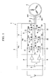
- FIG. 1 shows the configuration of a circuit 1 including a power control unit (PCU) of a hybrid vehicle related to one embodiment of the invention.
- the circuit 1 includes a battery 2 of a high-voltage type, a power control unit 3, and a motor 4.
- a battery 2 of a high-voltage type for example, an engine and the motor 4 directly connected to this engine are arranged in the engine room.
- the power control unit 3 and the battery 2 are arranged in a rear part of the cabin of the hybrid vehicle.
- the motor 4 and the power control unit 3 are mutually connected by a three-phase cable 5.
- a positive electrode line P of the power control unit 3 is connected to a positive electrode of the battery 2, and a negative electrode line N of the power control unit 3 is connected to a negative electrode of the battery 2.
- electric power is supplied to the power control unit 3 from the battery 2, and the motor 4 is driven in a state where the electric power voltage of the power control unit 3 is raised.
- the electric power voltage of the power control unit 3 is lowered, and the battery 2 is charged by the positive electrode line P and the negative electrode line N.
- the power control unit 3 is constituted by a power drive unit (PDU) 9.
- the power drive unit (PDU) 9 includes a smoothing capacitor 6, a gate drive substrate 7, and a bridge circuit 8.
- the bridge circuit 8 of the power drive unit 9 is configured so as to bridge-connect a high-side (high-potential-side) U-phase switching device (UH) 11, a low-side (low-potential-side) U-phase switching device (UL) 12, and a high-side V-phase switching device (VH) 21, and a low-side V-phase switching device (VL) 22, a high-side W-phase switching device (WH) 31, and a low-side W-phase switching device (WL) 32.
- the high-side U-phase switching device (UH) 11 and the low-side U-phase switching device (UL) 12 are connected using wiring, and the wiring is connected to the U-phase of a three-phase cable 5.
- the high-side V-phase switching device (VH) 21 and the low-side V-phase switching device (VL) 22 are connected using wiring, and the wiring is connected to the V phase of the three-phase cable 5.
- the high-side W-phase switching device (WH) 31 and the low-side W-phase switching device (WL) 32 are connected using wiring, and the wiring is connected to the W phase of the three-phase cable 5.
- the switching devices transistors, FETs (Field-effect Transistors), IGBTs (Insulated Gate Bipolar Transistors), or the like are used.
- the high-side U-phase switching device 11, the high-side V-phase switching device 21, and the high-side W-phase switching device 31 that are high-side switching devices are connected to the positive electrode line P, and these devices constitute a high-side arm.
- the low-side U-phase switching device 12, the low-side V-phase switching device 22, and the low-side W-phase switching device 32 that are low-side switching devices are connected to the negative electrode line N, and these devices constitute a low-side arm.
- a diode (DUH) 13, a diode (DUL) 14, a diode (DVH) 23, a diode (DVL) 24, a diode (DWH) 33, and a diode (DWL) 34 are connected, so as to arrange a forward direction from an emitter toward a collector between the collector and the emitter of each of the switching devices 11, 12, 21, 22, 31, and 32.
- the bridge circuit 8 and U-phase, V-phase, and W-phase coils of the motor 4 are connected by the three-phase cable 5.
- the three-phase cable 5 is constituted by three electrode lines of a third U electrodes line UOUT, a third V electrode line VOUT, and a third W electrode line WOUT.
- a current flows into the third U electrode line UOUT, the third V electrode line VOUT, and the third W electrode line WOUT.
- descriptions of not only symbol "OUT” but also symbol "IN” should also be made.
- only the description of "OUT" is used as the designation of respective parts to avoid complications.
- the high-side U-phase switching device 11, the low-side U-phase switching device 12, the diode 13, and the diode 14 are integrally molded as a U-phase motor drive circuit module 15 from resin.
- the high-side V-phase switching device 21, the low-side V-phase switching device 22, the diode 23, and the diode 24 are integrally molded as a V-phase motor drive circuit module 25 from resin.
- the high-side W-phase switching device 31, the low-side W-phase switching device 32, the diode 33, and the diode 34 are integrally molded as a W-phase motor drive circuit module 35 from resin. Accordingly, the U-phase motor drive circuit module 15, the V-phase motor drive circuit module 25, and the W-phase motor drive circuit module 35 are arranged between the positive electrode line P, the negative electrode line N, and the motor 4.
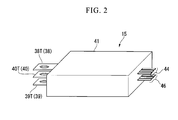
- FIG. 2 is a perspective view of a motor drive circuit module in the embodiment of the present invention.
- FIG. 3 shows an exploded perspective view of the U-phase motor drive circuit module 15.
- the V-phase motor drive circuit module 25 and the W-phase motor drive circuit module 35 also have the same configurations as the U-phase motor drive circuit module 15, descriptions thereof will be omitted.
- FIG. 4 is a circuit diagram of the motor drive circuit module.
- FIG. 5 is a cross-sectional view of the motor drive circuit module.
- an upper positive electrode 38 connected to the positive electrode line P a lower negative electrode 39 connected to the negative electrode line N
- reference numerals 38T, 39T, and 40T represent the terminal areas of the positive electrode 38, the negative electrode 39, and the OUT electrode 40, respectively, and protrude to the outside of the resin mold portion 41.
- the high-side U-phase switching device 11, the diode 13, and a signal terminal 43 are mounted together between the positive electrode 38 and the OUT electrode 40 via a solder layer 42 inside the resin mold portion 41.
- a signal line 44 of the signal terminal 43 protrudes to the outside of the resin mold portion.
- the low-side U-phase switching device 12, the diode 14, and a signal terminal 45 are mounted between the OUT electrode 40 and the negative electrode 39 via a solder layer 42 inside the resin mold portion 41.
- a signal line 46 of the signal terminal 45 also protrudes to the outside of the resin mold portion 41.
- Only the resin mold portion 41 is interposed between the positive electrode 38 and the OUT electrode 40 and between the OUT electrode 40 and the negative electrode 39 in the portion where the high-side U-phase switching device 11 and the diode 13, and the low-side U-phase switching device 12 and the diode 14 are not arranged, inside the resin mold portion 41.
- a positive electrode surface 38D of the positive electrode 38 and an OUT electrode surface 40D of the OUT electrode 40 face each other
- the OUT electrode surface 40D of the OUT electrode 40 and a negative electrode surface 39D of the negative electrode 39 face each other.
- the positive electrode 38, the OUT electrode 40, and the negative electrode 39 are arranged so that the direction of a current that flows through the positive electrode 38 and the direction of a current that flows through the OUT electrode 40 reverses direction (solid line arrow) when the current flows through the positive electrode 38. Moreover, an arrangement is made so that the direction of a current that flows through the negative electrode 39 and the direction of the current that flows through the OUT electrode 40 reverses direction (broken line arrow) when the current flows through the negative electrode 39.
- the positive electrode surface 38D of the positive electrode 38 and the OUT electrode surface 40D of the OUT electrode 40 face each other and the OUT electrode surface 40D of the OUT electrode 40 and the negative electrode surface 39D of the negative electrode 39 face each other. Also, an arrangement is made so that currents flow in opposite directions in the positive electrode 38 and the OUT electrode 40 when a current flows through the positive electrode 38 (solid line of FIG. 4 ), and an arrangement is made so that currents flow in opposite directions in the negative electrode 39 and the OUT electrode 40 when a current flows through the negative electrode 39 (broken line of FIG. 4 ). Therefore, the inductance can be effectively reduced by the mutual inductance effect.
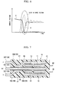
- FIG. 6 shows an example of the switching waveform of a related-art driving module and the switching waveform of the drive module in the embodiment of the present invention.
- the vertical axis shows a relative voltage value and a relative current value.
- the horizontal axis shows time.
- the inductance of wiring is generated in proportion to the distance between the positive electrode terminal 38T and the OUT electrode terminal 40T, and if a current I (solid line) decreases abruptly during a switching operation, a rise (chain line in FIG.
- the rise in this surge voltage can be suppressed as a voltage V shown by a solid line, loss and withstand voltage over (application of a voltage exceeding the withstand voltage of the switching devices) of the switching devices, or the like can be prevented.
- the middle portions of the positive electrode surface 38D and the OUT electrode surface 40D in the right-and-left direction of FIG. 7 approaches the OUT electrode surface 40D and the inductance offset portion 47 close to the OUT electrode surface 40D is formed.
- insulating materials 48 are interposed between the positive electrode surface 38D of the positive electrode 38 and the OUT electrode surface 40D of the OUT electrode 40 and between the OUT electrode surface 40D of the OUT electrode 40 and the negative electrode surface 39D of the negative electrode 39, which correspond to the inductance offset portions 47. Specifically, the insulating materials 48 are provided so as to cover the top and bottom surfaces of the OUT electrode surface 40D of the OUT electrode 40.
- the distance between the positive electrode surface 38D of the positive electrode 38 and the OUT electrode surface 40D of the OUT electrode 40 and the distance between the OUT electrode surface 40D of the OUT electrode 40 and the negative electrode surface 39D of the negative electrode 39 can be minimized by providing the insulating materials 48.
- the mutual inductance can be increased to make the overall inductance low.
- the inter-electrode distance and the mutual inductance effect have an inverse proportion relationship.
- the inter-electrode distance whose limit was, for example, about 3 mm in order to prevent short circuiting, can be less than or equal to 1 mm by adding the insulating materials 48. This enables a range with a large mutual effect to be used.
- the present invention is not limited only to the above embodiments and can be applied to vehicles that use a motor, such as an electric vehicle and a fuel cell vehicle, for a traveling driving force in addition to hybrid vehicles.
- a motor drive circuit module that can reduce the inductance effectively by mutual inductance can be provided.
Landscapes
- Engineering & Computer Science (AREA)
- Microelectronics & Electronic Packaging (AREA)
- Inverter Devices (AREA)
Abstract
In the disclosed motor-driving circuit module, a first electrode surface of a first electrode and a third electrode surface of a third electrode are arranged so as to face each other and such that current flows in opposite directions in the first electrode and the third electrode when a current runs through the first electrode. Also, a second electrode surface of a second electrode and the third electrode surface of the third electrode are arranged so as to face each other and such that current flows in opposite directions in the second electrode and the third electrode when a current runs through the second electrode.
Description
- The present invention relates to a motor drive circuit module.
Priority is claimed on Japanese Patent Application No.2010-075743, filed March 29, 2010 - In motor drive circuit modules used to drive a motor, the inductance of the wiring of a drive circuit causes a rise in surge voltage in a case where a switching device is switched to supply a motor driving current to a motor from a power source. If the surge voltage is high, power loss is incurred, and if the surge voltage exceeding the withstand voltage of the switching device is applied, degradation of the switching device is caused. In order to suppress this, applying currents in mutually opposite directions at the same time to further reduce inductance by a mutual inductance effect is performed.
-
- Patent Document 1: Japanese Unexamined Patent Application, First Publication No.
2005-261035 - However, since the switching device is horizontally set in the above related-art motor drive circuit modules, there is a problem in that the inductance cannot be sufficiently reduced.
- Thus, an object of the invention is to provide a motor drive circuit module that can reduce the inductance effectively using the mutual inductance effect.
- In order to achieve the above object, the invention has adopted the following:
- (1) One aspect of the present invention provides a motor drive circuit module provided in a power control unit that has a first electrode line connected to one electrode of a power source and a second electrode line connected to the other electrode of the power source and drives a motor with the electric power from the power source, and arranged between the first electrode line, the second electrode line, and the motor. The module includes, inside a resin mold portion in which switching devices are molded, a first electrode connected to the first electrode line; a second electrode connected to the second electrode line; and a third electrode connected to the motor. A first electrode surface of the first electrode and a third electrode surface of the third electrode are arranged so as to face each other and such that currents flow in opposite directions in the first electrode and the third electrode when a current flows through the first electrode, and a second electrode surface of the second electrode and the third electrode surface of the third electrode are arranged so as to face each other and such that currents flow in opposite directions in the second electrode and the third electrode when a current flows through the second electrode.
- (2) In the motor drive circuit module described in the above (1), a configuration may be adopted in which inductance offset portions are provided where the distance between the first electrode surface and the third electrode surface and the distance between the second output electrode surface and the third electrode surface are partially smaller than other portions, in a portion where the first electrode surface of the first electrode and the third electrode surface of the third electrode face each other and a portion where the second electrode surface of the second electrode and the third electrode surface of the third electrode face each other.
- (3) The motor drive circuit module described in the above (2) may further include insulating materials interposed between the first electrode surface of the first electrode and the third electrode surface of the third electrode and between the second electrode surface of the second electrode and the third electrode surface of the third electrode, which correspond to the inductance offset portions.
- According to the aspect described in the above (1), the first electrode surface of the first electrode and the third electrode surface of the third electrode face each other, the second electrode surface of the second electrode and the third electrode surface of the third electrode face each other, and currents flow in opposite directions. Therefore, the inductance can be effectively reduced by mutual inductance.
In the case described in the above (2), the inductance can be further reduced by providing the inductance offset portions where the distance between the first electrode surface of the first electrode and the third electrode surface of the third electrode surface and the distance between the second electrode surface of the second electrode and the third electrode surface of the third electrode becomes smaller.
In the case described in the above (3), the insulating materials are provided, so that the distance between the first electrode surface of the first electrode and the third electrode surface of the third electrode and the distance between the second electrode surface of the second electrode and the third electrode surface of the third electrode can be minimized and the inductance can be minimized. -
-
FIG. 1 is a circuit diagram of a motor drive circuit device in one embodiment of the invention; -
FIG. 2 is a perspective view of a motor drive circuit module in the embodiment; -
FIG. 3 is an exploded perspective view of the motor drive circuit module; -
FIG. 4 is a circuit diagram of the motor drive circuit module; -
FIG. 5 is a cross-sectional view of the motor drive circuit module; -
FIG. 6 is a graph showing changes in a surge voltage during switching in the embodiment and showing a situation where the surge voltage is suppressed; -
FIG. 7 is a view showing a motor drive circuit module in another embodiment of the invention, and is a cross-sectional view corresponding toFIG. 5 ; and -
FIG. 8 is a graph showing the relationship between inter-electrode distance and the mutual inductance effect in the embodiment. - Embodiments of the invention will be described below with reference to the accompanying drawings.
FIG. 1 shows the configuration of a circuit 1 including a power control unit (PCU) of a hybrid vehicle related to one embodiment of the invention. The circuit 1 includes abattery 2 of a high-voltage type, a power control unit 3, and a motor 4. In the hybrid vehicle, for example, an engine and the motor 4 directly connected to this engine are arranged in the engine room. The power control unit 3 and thebattery 2 are arranged in a rear part of the cabin of the hybrid vehicle. The motor 4 and the power control unit 3 are mutually connected by a three-phase cable 5. - A positive electrode line P of the power control unit 3 is connected to a positive electrode of the
battery 2, and a negative electrode line N of the power control unit 3 is connected to a negative electrode of thebattery 2. Thereby, electric power is supplied to the power control unit 3 from thebattery 2, and the motor 4 is driven in a state where the electric power voltage of the power control unit 3 is raised. In a case where the motor 4 performs a regenerative operation, the electric power voltage of the power control unit 3 is lowered, and thebattery 2 is charged by the positive electrode line P and the negative electrode line N. The power control unit 3 is constituted by a power drive unit (PDU) 9. The power drive unit (PDU) 9 includes a smoothing capacitor 6, a gate drive substrate 7, and abridge circuit 8. - The
bridge circuit 8 of thepower drive unit 9 is configured so as to bridge-connect a high-side (high-potential-side) U-phase switching device (UH) 11, a low-side (low-potential-side) U-phase switching device (UL) 12, and a high-side V-phase switching device (VH) 21, and a low-side V-phase switching device (VL) 22, a high-side W-phase switching device (WH) 31, and a low-side W-phase switching device (WL) 32. Here, the high-side U-phase switching device (UH) 11 and the low-side U-phase switching device (UL) 12 are connected using wiring, and the wiring is connected to the U-phase of a three-phase cable 5. The high-side V-phase switching device (VH) 21 and the low-side V-phase switching device (VL) 22 are connected using wiring, and the wiring is connected to the V phase of the three-phase cable 5. The high-side W-phase switching device (WH) 31 and the low-side W-phase switching device (WL) 32 are connected using wiring, and the wiring is connected to the W phase of the three-phase cable 5. Here, as the switching devices, transistors, FETs (Field-effect Transistors), IGBTs (Insulated Gate Bipolar Transistors), or the like are used. - The high-side
U-phase switching device 11, the high-side V-phase switching device 21, and the high-side W-phase switching device 31 that are high-side switching devices are connected to the positive electrode line P, and these devices constitute a high-side arm. The low-sideU-phase switching device 12, the low-side V-phase switching device 22, and the low-side W-phase switching device 32 that are low-side switching devices are connected to the negative electrode line N, and these devices constitute a low-side arm. - An example in which bipolar transistors are used as the switching devices is shown. A diode (DUH) 13, a diode (DUL) 14, a diode (DVH) 23, a diode (DVL) 24, a diode (DWH) 33, and a diode (DWL) 34 are connected, so as to arrange a forward direction from an emitter toward a collector between the collector and the emitter of each of the
switching devices
Thebridge circuit 8 and U-phase, V-phase, and W-phase coils of the motor 4 are connected by the three-phase cable 5. The three-phase cable 5 is constituted by three electrode lines of a third U electrodes line UOUT, a third V electrode line VOUT, and a third W electrode line WOUT.
Here, in a case where the motor 4 is made to perform a regenerative operation, if a current flows into the third U electrode line UOUT, the third V electrode line VOUT, and the third W electrode line WOUT, descriptions of not only symbol "OUT" but also symbol "IN" should also be made. However, only the description of "OUT" is used as the designation of respective parts to avoid complications. - Here, the high-side
U-phase switching device 11, the low-sideU-phase switching device 12, thediode 13, and thediode 14 are integrally molded as a U-phase motordrive circuit module 15 from resin. The high-side V-phase switching device 21, the low-side V-phase switching device 22, thediode 23, and thediode 24 are integrally molded as a V-phase motordrive circuit module 25 from resin. The high-side W-phase switching device 31, the low-side W-phase switching device 32, thediode 33, and thediode 34 are integrally molded as a W-phase motordrive circuit module 35 from resin.
Accordingly, the U-phase motordrive circuit module 15, the V-phase motordrive circuit module 25, and the W-phase motordrive circuit module 35 are arranged between the positive electrode line P, the negative electrode line N, and the motor 4. -
FIG. 2 is a perspective view of a motor drive circuit module in the embodiment of the present invention.
FIG. 3 shows an exploded perspective view of the U-phase motordrive circuit module 15. In addition, since the V-phase motordrive circuit module 25 and the W-phase motordrive circuit module 35 also have the same configurations as the U-phase motordrive circuit module 15, descriptions thereof will be omitted. -
FIG. 4 is a circuit diagram of the motor drive circuit module.FIG. 5 is a cross-sectional view of the motor drive circuit module. As shown inFIGS. 2 to 5 , in the U-phase motordrive circuit module 15, an upperpositive electrode 38 connected to the positive electrode line P, a lowernegative electrode 39 connected to the negative electrode line N, and anOUT electrode 40 that is arranged between thepositive electrode 38 and thenegative electrode 39 and connected to the third U electrode line UOUT are stacked so as to overlap each other as seen from the top face. These are molded by aresin mold portion 41. In addition,reference numerals positive electrode 38, thenegative electrode 39, and theOUT electrode 40, respectively, and protrude to the outside of theresin mold portion 41. - As shown in
FIG. 3 , the high-side U-phase switchingdevice 11, thediode 13, and asignal terminal 43 are mounted together between thepositive electrode 38 and theOUT electrode 40 via asolder layer 42 inside theresin mold portion 41. Asignal line 44 of thesignal terminal 43 protrudes to the outside of the resin mold portion.
The low-side U-phase switchingdevice 12, thediode 14, and asignal terminal 45 are mounted between theOUT electrode 40 and thenegative electrode 39 via asolder layer 42 inside theresin mold portion 41. Asignal line 46 of thesignal terminal 45 also protrudes to the outside of theresin mold portion 41. - Only the
resin mold portion 41 is interposed between thepositive electrode 38 and theOUT electrode 40 and between theOUT electrode 40 and thenegative electrode 39 in the portion where the high-side U-phase switchingdevice 11 and thediode 13, and the low-side U-phase switchingdevice 12 and thediode 14 are not arranged, inside theresin mold portion 41. In that portion, apositive electrode surface 38D of thepositive electrode 38 and anOUT electrode surface 40D of theOUT electrode 40 face each other, and theOUT electrode surface 40D of theOUT electrode 40 and anegative electrode surface 39D of thenegative electrode 39 face each other.
Additionally, as shown inFIG. 4 , thepositive electrode 38, theOUT electrode 40, and thenegative electrode 39 are arranged so that the direction of a current that flows through thepositive electrode 38 and the direction of a current that flows through theOUT electrode 40 reverses direction (solid line arrow) when the current flows through thepositive electrode 38. Moreover, an arrangement is made so that the direction of a current that flows through thenegative electrode 39 and the direction of the current that flows through theOUT electrode 40 reverses direction (broken line arrow) when the current flows through thenegative electrode 39. - According to the above embodiment, as shown in
FIG. 5 , within theresin mold portion 41, thepositive electrode surface 38D of thepositive electrode 38 and theOUT electrode surface 40D of theOUT electrode 40 face each other and theOUT electrode surface 40D of theOUT electrode 40 and thenegative electrode surface 39D of thenegative electrode 39 face each other. Also, an arrangement is made so that currents flow in opposite directions in thepositive electrode 38 and theOUT electrode 40 when a current flows through the positive electrode 38 (solid line ofFIG. 4 ), and an arrangement is made so that currents flow in opposite directions in thenegative electrode 39 and theOUT electrode 40 when a current flows through the negative electrode 39 (broken line ofFIG. 4 ). Therefore, the inductance can be effectively reduced by the mutual inductance effect. -
FIG. 6 shows an example of the switching waveform of a related-art driving module and the switching waveform of the drive module in the embodiment of the present invention. The vertical axis shows a relative voltage value and a relative current value. The horizontal axis shows time.
In a case where an arrangement where thepositive electrode 38 and theOUT electrode 40 do not face each other but extend in separate directions like the related art is adopted (in a case where theOUT electrode 40 extends to the right side referring toFIG. 5 ), the inductance of wiring is generated in proportion to the distance between thepositive electrode terminal 38T and theOUT electrode terminal 40T, and if a current I (solid line) decreases abruptly during a switching operation, a rise (chain line inFIG. 6 ) in a surge voltage whose voltage rises up abruptly occurs. In contrast, according to the embodiment of the present invention, the rise in this surge voltage can be suppressed as a voltage V shown by a solid line, loss and withstand voltage over (application of a voltage exceeding the withstand voltage of the switching devices) of the switching devices, or the like can be prevented. - That is, if the
positive electrode surface 38D of thepositive electrode 38 and theOUT electrode surface 40D of theOUT electrode 40 inFIG. 5 are taken as an example, mutual induction occurs as thepositive electrode surface 38D and theOUT electrode surface 40D are arranged to face each other. Thereby, since an induced electromotive force determined by mutual inductance is generated if a current flows through thepositive electrode surface 38D of thepositive electrode 38, and is mutually offset by an induced electromotive force determined by the mutual inductance produced by a current that flows to theOUT electrode surface 40D of theOUT electrode 40 in a direction opposite to the current of thepositive electrode surface 38D (mutual inductance effect), the overall inductance can be reduced as a result. - Next, another embodiment of the present invention will be described with reference to
FIGS. 7 and8 .
As shown inFIG. 7 , in this embodiment, an inductance offsetportion 47 where the distance between thepositive electrode surface 38D of thepositive electrode 38 and theOUT electrode surface 40D of theOUT electrode 40 is partially smaller than the other portions, and an inductance offsetportion 47 where the distance between theOUT electrode surface 40D of theOUT electrode 40 and thenegative electrode surface 39D of thenegative electrode 39 is partially smaller than the other portions are provided, in thepositive electrode surface 38D of thepositive electrode 38 and theOUT electrode surface 40D of theOUT electrode 40, and theOUT electrode surface 40D of theOUT electrode 40 and thenegative electrode surface 39D of thenegative electrode 39, which face each other in the first embodiment. Specifically, the middle portions of thepositive electrode surface 38D and theOUT electrode surface 40D in the right-and-left direction ofFIG. 7 approaches theOUT electrode surface 40D and the inductance offsetportion 47 close to theOUT electrode surface 40D is formed. - Also, insulating
materials 48 are interposed between thepositive electrode surface 38D of thepositive electrode 38 and theOUT electrode surface 40D of theOUT electrode 40 and between theOUT electrode surface 40D of theOUT electrode 40 and thenegative electrode surface 39D of thenegative electrode 39, which correspond to the inductance offsetportions 47. Specifically, the insulatingmaterials 48 are provided so as to cover the top and bottom surfaces of theOUT electrode surface 40D of theOUT electrode 40. - Accordingly, in this embodiment, the distance between the
positive electrode surface 38D of thepositive electrode 38 and theOUT electrode surface 40D of theOUT electrode 40 and the distance between theOUT electrode surface 40D of theOUT electrode 40 and thenegative electrode surface 39D of thenegative electrode 39 can be minimized by providing the insulatingmaterials 48. Thus, the mutual inductance can be increased to make the overall inductance low. - That is, as shown in
FIG. 8 , the inter-electrode distance and the mutual inductance effect have an inverse proportion relationship. However, in a case where the insulatingmaterials 48 are not provided (only the resin mold portion is provided), the inter-electrode distance, whose limit was, for example, about 3 mm in order to prevent short circuiting, can be less than or equal to 1 mm by adding the insulatingmaterials 48. This enables a range with a large mutual effect to be used.
In addition, the present invention is not limited only to the above embodiments and can be applied to vehicles that use a motor, such as an electric vehicle and a fuel cell vehicle, for a traveling driving force in addition to hybrid vehicles. - A motor drive circuit module that can reduce the inductance effectively by mutual inductance can be provided.
-
- 2
- BATTERY (POWER SOURCE)
- P
- POSITIVE ELECTRODE LINE (FIRST ELECTRODE LINE)
- N
- NEGATIVE ELECTRODE LINE (SECOND ELECTRODE LINE)
- 4
- MOTOR
- 3
- POWER CONTROL UNIT
- 15
- U-PHASE MOTOR DRIVE CIRCUIT MODULE
- 25
- V-PHASE MOTOR DRIVE CIRCUIT MODULE
- 35
- W-PHASE MOTOR DRIVE CIRCUIT MODULE
- 11
- HIGH-SIDE U-PHASE SWITCHING DEVICE
- 12
- LOW-SIDE U-PHASE SWITCHING DEVICE
- 21
- HIGH-SIDE V-PHASE SWITCHING DEVICE
- 22
- LOW-SIDE V-PHASE SWITCHING DEVICE
- 31
- HIGH-SIDE W-PHASE SWITCHING DEVICE
- 32
- LOW-SIDE W-PHASE SWITCHING DEVICE
- 41
- RESIN MOLD PORTION
- 38
- POSITIVE ELECTRODE (FIRST ELECTRODE)
- 39
- NEGATIVE ELECTRODE (SECOND ELECTRODE)
- 40
- OUT ELECTRODE (THIRD ELECTRODE)
- 38D
- POSITIVE ELECTRODE SURFACE (FIRST ELECTRODE SURFACE)
- 39D
- NEGATIVE ELECTRODE SURFACE (SECOND ELECTRODE SURFACE)
- 40D
- OUT ELECTRODE SURFACE (THIRD ELECTRODE SURFACE)
- 47
- INDUCTANCE OFFSET PORTION
- 48
- INSULATING MATERIAL
Claims (3)
- A motor drive circuit module provided in a power control unit that has a first electrode line connected to one electrode of a power source and a second electrode line connected to the other electrode of the power source and drives a motor with the electric power from the power source, and arranged between the first electrode line, the second electrode line, and the motor, the module comprising:inside a resin mold portion in which switching devices are molded,
a first electrode connected to the first electrode line;
a second electrode connected to the second electrode line; and
a third electrode connected to the motor,
wherein a first electrode surface of the first electrode and a third electrode surface of the third electrode are arranged so as to face each other and such that currents flow in opposite directions in the first electrode and the third electrode when a current flows through the first electrode, and
wherein a second electrode surface of the second electrode and the third electrode surface of the third electrode are arranged so as to face each other and such that currents flow in opposite directions in the second electrode and the third electrode when a current flows through the second electrode. - The motor drive circuit module according to claim 1,
wherein inductance offset portions where the distance between the first electrode surface and the third electrode surface and the distance between the second output electrode surface and the third electrode surface are partially smaller than other portions are provided, in a portion where the first electrode surface of the first electrode and the third electrode surface of the third electrode face each other and a portion where the second electrode surface of the second electrode and the third electrode surface of the third electrode face each other. - The motor drive circuit module according to claim 2, further comprising:insulating materials interposed between the first electrode surface of the first electrode and the third electrode surface of the third electrode and between the second electrode surface of the second electrode and the third electrode surface of the third electrode, which correspond to the inductance offset portions.
Applications Claiming Priority (2)
| Application Number | Priority Date | Filing Date | Title |
|---|---|---|---|
| JP2010075743 | 2010-03-29 | ||
| PCT/JP2011/055503 WO2011122279A1 (en) | 2010-03-29 | 2011-03-09 | Motor drive circuit module |
Publications (1)
| Publication Number | Publication Date |
|---|---|
| EP2555406A1 true EP2555406A1 (en) | 2013-02-06 |
Family
ID=44712004
Family Applications (1)
| Application Number | Title | Priority Date | Filing Date |
|---|---|---|---|
| EP11762519A Withdrawn EP2555406A1 (en) | 2010-03-29 | 2011-03-09 | Motor drive circuit module |
Country Status (5)
| Country | Link |
|---|---|
| US (1) | US20130069573A1 (en) |
| EP (1) | EP2555406A1 (en) |
| JP (1) | JPWO2011122279A1 (en) |
| CN (1) | CN102812629A (en) |
| WO (1) | WO2011122279A1 (en) |
Cited By (2)
| Publication number | Priority date | Publication date | Assignee | Title |
|---|---|---|---|---|
| WO2018052683A1 (en) * | 2016-09-19 | 2018-03-22 | General Electric Company | Electronic module assembly having low loop inductance |
| CN108319995A (en) * | 2018-01-15 | 2018-07-24 | 苏州互盟信息存储技术有限公司 | A kind of USB memory card data read-write equipment |
Families Citing this family (9)
| Publication number | Priority date | Publication date | Assignee | Title |
|---|---|---|---|---|
| JP5798951B2 (en) * | 2012-03-02 | 2015-10-21 | 日立オートモティブシステムズ株式会社 | Inverter device |
| JP5811072B2 (en) * | 2012-11-02 | 2015-11-11 | トヨタ自動車株式会社 | Power module |
| KR102034717B1 (en) * | 2013-02-07 | 2019-10-21 | 삼성전자주식회사 | Substrate and terminals for power module and power module comprising the same |
| JP2014183078A (en) * | 2013-03-18 | 2014-09-29 | Mitsubishi Electric Corp | Semiconductor device |
| CN103354414B (en) * | 2013-06-17 | 2016-02-24 | 许继电气股份有限公司 | A kind of parallel IGBT power unit |
| JP2015173147A (en) | 2014-03-11 | 2015-10-01 | 株式会社東芝 | semiconductor device |
| JP6326038B2 (en) * | 2015-12-24 | 2018-05-16 | 太陽誘電株式会社 | Electrical circuit device |
| JP7666781B2 (en) * | 2021-11-11 | 2025-04-22 | 新光電気工業株式会社 | Semiconductor Device |
| JP2024063837A (en) * | 2022-10-27 | 2024-05-14 | 新光電気工業株式会社 | Semiconductor Device |
Family Cites Families (11)
| Publication number | Priority date | Publication date | Assignee | Title |
|---|---|---|---|---|
| JPS62144578A (en) * | 1985-12-17 | 1987-06-27 | Mitsubishi Electric Corp | Inverter circuit |
| JP3460973B2 (en) * | 1999-12-27 | 2003-10-27 | 三菱電機株式会社 | Power converter |
| JP3692906B2 (en) * | 2000-05-25 | 2005-09-07 | 日産自動車株式会社 | Power wiring structure and semiconductor device |
| JP3637846B2 (en) * | 2000-06-30 | 2005-04-13 | 日産自動車株式会社 | Wiring structure |
| JP2004056984A (en) * | 2002-07-24 | 2004-02-19 | Mitsubishi Electric Corp | Power converter |
| JP4039202B2 (en) * | 2002-10-16 | 2008-01-30 | 日産自動車株式会社 | Stacked semiconductor device and assembly method thereof |
| JP2005261035A (en) | 2004-03-10 | 2005-09-22 | Toyota Motor Corp | Semiconductor device |
| JP4820233B2 (en) * | 2006-08-09 | 2011-11-24 | 本田技研工業株式会社 | Semiconductor device |
| JP4919062B2 (en) * | 2007-07-06 | 2012-04-18 | 富士電機株式会社 | Parallel wiring conductor structure |
| JP5407198B2 (en) * | 2008-07-02 | 2014-02-05 | 富士電機株式会社 | Power module for power converter |
| JP4851601B2 (en) | 2010-01-08 | 2012-01-11 | タイヨーエレック株式会社 | Game machine |
-
2011
- 2011-03-09 JP JP2012508183A patent/JPWO2011122279A1/en active Pending
- 2011-03-09 WO PCT/JP2011/055503 patent/WO2011122279A1/en not_active Ceased
- 2011-03-09 CN CN201180015237.1A patent/CN102812629A/en active Pending
- 2011-03-09 US US13/637,935 patent/US20130069573A1/en not_active Abandoned
- 2011-03-09 EP EP11762519A patent/EP2555406A1/en not_active Withdrawn
Non-Patent Citations (1)
| Title |
|---|
| See references of WO2011122279A1 * |
Cited By (4)
| Publication number | Priority date | Publication date | Assignee | Title |
|---|---|---|---|---|
| WO2018052683A1 (en) * | 2016-09-19 | 2018-03-22 | General Electric Company | Electronic module assembly having low loop inductance |
| US10021802B2 (en) | 2016-09-19 | 2018-07-10 | General Electric Company | Electronic module assembly having low loop inductance |
| CN108319995A (en) * | 2018-01-15 | 2018-07-24 | 苏州互盟信息存储技术有限公司 | A kind of USB memory card data read-write equipment |
| CN108319995B (en) * | 2018-01-15 | 2020-11-27 | 苏州互盟信息存储技术有限公司 | USB memory card data read-write device |
Also Published As
| Publication number | Publication date |
|---|---|
| US20130069573A1 (en) | 2013-03-21 |
| WO2011122279A1 (en) | 2011-10-06 |
| JPWO2011122279A1 (en) | 2013-07-08 |
| CN102812629A (en) | 2012-12-05 |
Similar Documents
| Publication | Publication Date | Title |
|---|---|---|
| EP2555406A1 (en) | Motor drive circuit module | |
| JP6785276B2 (en) | Power converter | |
| US8519561B2 (en) | Power module and vehicle-mounted inverter using the same | |
| US9425707B2 (en) | Inverter device capable of appropriately fixing a power module having a switching element and a smoothing capacitor in a limited region | |
| US11348855B2 (en) | Semiconductor component and power module | |
| US11424689B2 (en) | Power conversion device | |
| US9906158B2 (en) | Power conversion device | |
| JP6426465B2 (en) | Power converter | |
| JP5975789B2 (en) | Power semiconductor module | |
| CN115149772A (en) | Power module for inverter and inverter including the same | |
| CN118077131A (en) | Power conversion device | |
| US7768149B2 (en) | Power module | |
| CN102369655A (en) | Noise reduction device associated with a three-phase brushless motor | |
| US11437305B2 (en) | Semiconductor module | |
| JP2010035369A (en) | Conductor arrangement structure of power converter and power conversion unit | |
| US10749400B2 (en) | Bus bar unit | |
| US20120140412A1 (en) | Power module for inverter | |
| WO2023063086A1 (en) | Power conversion device | |
| JP2013223384A (en) | Power conversion apparatus and vehicle | |
| US20250226762A1 (en) | Output potential switching circuit | |
| CN121620866A (en) | Semiconductor module and power conversion device | |
| CN115473421A (en) | Discharge device | |
| JP2004229393A (en) | Semiconductor device | |
| CN121485442A (en) | Dual Inverter System | |
| JP2014183638A (en) | Power conversion device |
Legal Events
| Date | Code | Title | Description |
|---|---|---|---|
| PUAI | Public reference made under article 153(3) epc to a published international application that has entered the european phase |
Free format text: ORIGINAL CODE: 0009012 |
|
| 17P | Request for examination filed |
Effective date: 20121009 |
|
| AK | Designated contracting states |
Kind code of ref document: A1 Designated state(s): AL AT BE BG CH CY CZ DE DK EE ES FI FR GB GR HR HU IE IS IT LI LT LU LV MC MK MT NL NO PL PT RO RS SE SI SK SM TR |
|
| DAX | Request for extension of the european patent (deleted) | ||
| STAA | Information on the status of an ep patent application or granted ep patent |
Free format text: STATUS: THE APPLICATION HAS BEEN WITHDRAWN |
|
| 18W | Application withdrawn |
Effective date: 20140718 |