EP2555246A1 - Semiconductor device and method for producing same - Google Patents
Semiconductor device and method for producing same Download PDFInfo
- Publication number
- EP2555246A1 EP2555246A1 EP10848493A EP10848493A EP2555246A1 EP 2555246 A1 EP2555246 A1 EP 2555246A1 EP 10848493 A EP10848493 A EP 10848493A EP 10848493 A EP10848493 A EP 10848493A EP 2555246 A1 EP2555246 A1 EP 2555246A1
- Authority
- EP
- European Patent Office
- Prior art keywords
- substrate
- semiconductor device
- layer
- insulating film
- manufacturing
- Prior art date
- Legal status (The legal status is an assumption and is not a legal conclusion. Google has not performed a legal analysis and makes no representation as to the accuracy of the status listed.)
- Withdrawn
Links
Images







Classifications
-
- H—ELECTRICITY
- H10—SEMICONDUCTOR DEVICES; ELECTRIC SOLID-STATE DEVICES NOT OTHERWISE PROVIDED FOR
- H10D—INORGANIC ELECTRIC SEMICONDUCTOR DEVICES
- H10D30/00—Field-effect transistors [FET]
- H10D30/60—Insulated-gate field-effect transistors [IGFET]
- H10D30/64—Double-diffused metal-oxide semiconductor [DMOS] FETs
- H10D30/66—Vertical DMOS [VDMOS] FETs
-
- H—ELECTRICITY
- H10—SEMICONDUCTOR DEVICES; ELECTRIC SOLID-STATE DEVICES NOT OTHERWISE PROVIDED FOR
- H10D—INORGANIC ELECTRIC SEMICONDUCTOR DEVICES
- H10D1/00—Resistors, capacitors or inductors
- H10D1/60—Capacitors
- H10D1/62—Capacitors having potential barriers
- H10D1/66—Conductor-insulator-semiconductor capacitors, e.g. MOS capacitors
-
- H—ELECTRICITY
- H10—SEMICONDUCTOR DEVICES; ELECTRIC SOLID-STATE DEVICES NOT OTHERWISE PROVIDED FOR
- H10D—INORGANIC ELECTRIC SEMICONDUCTOR DEVICES
- H10D12/00—Bipolar devices controlled by the field effect, e.g. insulated-gate bipolar transistors [IGBT]
- H10D12/01—Manufacture or treatment
- H10D12/031—Manufacture or treatment of IGBTs
-
- H—ELECTRICITY
- H10—SEMICONDUCTOR DEVICES; ELECTRIC SOLID-STATE DEVICES NOT OTHERWISE PROVIDED FOR
- H10D—INORGANIC ELECTRIC SEMICONDUCTOR DEVICES
- H10D30/00—Field-effect transistors [FET]
- H10D30/01—Manufacture or treatment
- H10D30/021—Manufacture or treatment of FETs having insulated gates [IGFET]
- H10D30/028—Manufacture or treatment of FETs having insulated gates [IGFET] of double-diffused metal oxide semiconductor [DMOS] FETs
- H10D30/0291—Manufacture or treatment of FETs having insulated gates [IGFET] of double-diffused metal oxide semiconductor [DMOS] FETs of vertical DMOS [VDMOS] FETs
-
- H—ELECTRICITY
- H10—SEMICONDUCTOR DEVICES; ELECTRIC SOLID-STATE DEVICES NOT OTHERWISE PROVIDED FOR
- H10D—INORGANIC ELECTRIC SEMICONDUCTOR DEVICES
- H10D62/00—Semiconductor bodies, or regions thereof, of devices having potential barriers
- H10D62/40—Crystalline structures
- H10D62/405—Orientations of crystalline planes
-
- H—ELECTRICITY
- H10—SEMICONDUCTOR DEVICES; ELECTRIC SOLID-STATE DEVICES NOT OTHERWISE PROVIDED FOR
- H10D—INORGANIC ELECTRIC SEMICONDUCTOR DEVICES
- H10D62/00—Semiconductor bodies, or regions thereof, of devices having potential barriers
- H10D62/80—Semiconductor bodies, or regions thereof, of devices having potential barriers characterised by the materials
- H10D62/83—Semiconductor bodies, or regions thereof, of devices having potential barriers characterised by the materials being Group IV materials, e.g. B-doped Si or undoped Ge
- H10D62/832—Semiconductor bodies, or regions thereof, of devices having potential barriers characterised by the materials being Group IV materials, e.g. B-doped Si or undoped Ge being Group IV materials comprising two or more elements, e.g. SiGe
- H10D62/8325—Silicon carbide
-
- H—ELECTRICITY
- H10—SEMICONDUCTOR DEVICES; ELECTRIC SOLID-STATE DEVICES NOT OTHERWISE PROVIDED FOR
- H10D—INORGANIC ELECTRIC SEMICONDUCTOR DEVICES
- H10D64/00—Electrodes of devices having potential barriers
- H10D64/01—Manufacture or treatment
- H10D64/013—Manufacture or treatment of electrodes having a conductor capacitively coupled to a semiconductor by an insulator
- H10D64/01366—Manufacture or treatment of electrodes having a conductor capacitively coupled to a semiconductor by an insulator the semiconductor being silicon carbide
-
- H—ELECTRICITY
- H10—SEMICONDUCTOR DEVICES; ELECTRIC SOLID-STATE DEVICES NOT OTHERWISE PROVIDED FOR
- H10D—INORGANIC ELECTRIC SEMICONDUCTOR DEVICES
- H10D64/00—Electrodes of devices having potential barriers
- H10D64/60—Electrodes characterised by their materials
- H10D64/66—Electrodes having a conductor capacitively coupled to a semiconductor by an insulator, e.g. MIS electrodes
- H10D64/68—Electrodes having a conductor capacitively coupled to a semiconductor by an insulator, e.g. MIS electrodes characterised by the insulator, e.g. by the gate insulator
- H10D64/693—Electrodes having a conductor capacitively coupled to a semiconductor by an insulator, e.g. MIS electrodes characterised by the insulator, e.g. by the gate insulator the insulator comprising nitrogen, e.g. nitrides, oxynitrides or nitrogen-doped materials
-
- H—ELECTRICITY
- H10—SEMICONDUCTOR DEVICES; ELECTRIC SOLID-STATE DEVICES NOT OTHERWISE PROVIDED FOR
- H10P—GENERIC PROCESSES OR APPARATUS FOR THE MANUFACTURE OR TREATMENT OF DEVICES COVERED BY CLASS H10
- H10P14/00—Formation of materials, e.g. in the shape of layers or pillars
- H10P14/20—Formation of materials, e.g. in the shape of layers or pillars of semiconductor materials
- H10P14/29—Formation of materials, e.g. in the shape of layers or pillars of semiconductor materials characterised by the substrates
- H10P14/2901—Materials
- H10P14/2902—Materials being Group IVA materials
- H10P14/2904—Silicon carbide
-
- H—ELECTRICITY
- H10—SEMICONDUCTOR DEVICES; ELECTRIC SOLID-STATE DEVICES NOT OTHERWISE PROVIDED FOR
- H10P—GENERIC PROCESSES OR APPARATUS FOR THE MANUFACTURE OR TREATMENT OF DEVICES COVERED BY CLASS H10
- H10P14/00—Formation of materials, e.g. in the shape of layers or pillars
- H10P14/20—Formation of materials, e.g. in the shape of layers or pillars of semiconductor materials
- H10P14/29—Formation of materials, e.g. in the shape of layers or pillars of semiconductor materials characterised by the substrates
- H10P14/2926—Crystal orientations
-
- H—ELECTRICITY
- H10—SEMICONDUCTOR DEVICES; ELECTRIC SOLID-STATE DEVICES NOT OTHERWISE PROVIDED FOR
- H10P—GENERIC PROCESSES OR APPARATUS FOR THE MANUFACTURE OR TREATMENT OF DEVICES COVERED BY CLASS H10
- H10P14/00—Formation of materials, e.g. in the shape of layers or pillars
- H10P14/20—Formation of materials, e.g. in the shape of layers or pillars of semiconductor materials
- H10P14/32—Formation of materials, e.g. in the shape of layers or pillars of semiconductor materials characterised by intermediate layers between substrates and deposited layers
- H10P14/3202—Materials thereof
- H10P14/3204—Materials thereof being Group IVA semiconducting materials
- H10P14/3208—Silicon carbide
-
- H—ELECTRICITY
- H10—SEMICONDUCTOR DEVICES; ELECTRIC SOLID-STATE DEVICES NOT OTHERWISE PROVIDED FOR
- H10P—GENERIC PROCESSES OR APPARATUS FOR THE MANUFACTURE OR TREATMENT OF DEVICES COVERED BY CLASS H10
- H10P14/00—Formation of materials, e.g. in the shape of layers or pillars
- H10P14/20—Formation of materials, e.g. in the shape of layers or pillars of semiconductor materials
- H10P14/34—Deposited materials, e.g. layers
- H10P14/3402—Deposited materials, e.g. layers characterised by the chemical composition
- H10P14/3404—Deposited materials, e.g. layers characterised by the chemical composition being Group IVA materials
- H10P14/3408—Silicon carbide
-
- H—ELECTRICITY
- H10—SEMICONDUCTOR DEVICES; ELECTRIC SOLID-STATE DEVICES NOT OTHERWISE PROVIDED FOR
- H10P—GENERIC PROCESSES OR APPARATUS FOR THE MANUFACTURE OR TREATMENT OF DEVICES COVERED BY CLASS H10
- H10P14/00—Formation of materials, e.g. in the shape of layers or pillars
- H10P14/20—Formation of materials, e.g. in the shape of layers or pillars of semiconductor materials
- H10P14/34—Deposited materials, e.g. layers
- H10P14/3466—Crystal orientation
-
- H—ELECTRICITY
- H10—SEMICONDUCTOR DEVICES; ELECTRIC SOLID-STATE DEVICES NOT OTHERWISE PROVIDED FOR
- H10P—GENERIC PROCESSES OR APPARATUS FOR THE MANUFACTURE OR TREATMENT OF DEVICES COVERED BY CLASS H10
- H10P90/00—Preparation of wafers not covered by a single main group of this subclass, e.g. wafer reinforcement
- H10P90/19—Preparing inhomogeneous wafers
- H10P90/1904—Preparing vertically inhomogeneous wafers
- H10P90/1906—Preparing SOI wafers
- H10P90/1914—Preparing SOI wafers using bonding
-
- H—ELECTRICITY
- H10—SEMICONDUCTOR DEVICES; ELECTRIC SOLID-STATE DEVICES NOT OTHERWISE PROVIDED FOR
- H10D—INORGANIC ELECTRIC SEMICONDUCTOR DEVICES
- H10D12/00—Bipolar devices controlled by the field effect, e.g. insulated-gate bipolar transistors [IGBT]
- H10D12/01—Manufacture or treatment
- H10D12/031—Manufacture or treatment of IGBTs
- H10D12/032—Manufacture or treatment of IGBTs of vertical IGBTs
Definitions
- electrode forming step (S60) is performed as shown in Fig. 17 , thereby obtaining semiconductor device 1 shown in Fig. 15 .
- the following describes another method for manufacturing the substrate constituting the semiconductor device of the present invention, with reference to Fig. 21 to Fig. 24 .
- the method for manufacturing the substrate in the sixth embodiment is performed in basically the same manner as that of the fifth embodiment.
- the method for manufacturing the substrate in the sixth embodiment is different from that of the fifth embodiment in terms of the process of forming base layer 110.
- step (S170) the heating step is performed.
- the stacked substrate fabricated in step (S130) is heated to approximately 1000°C in an inert gas atmosphere such as argon, for example.
- an inert gas atmosphere such as argon, for example.
- at least a portion of the metal film is silicided to form ohmic contact layer 150 making ohmic contact with base layer 110 and SiC layer 120.
- substrate 2 of the ninth embodiment can be readily manufactured in which base layer 110 and SiC layer 120 different in impurity concentration are connected to each other by ohmic contact layer 150, for example.
- step (S 130) SiC substrate 120 is placed on and in contact with precursor layer 161 formed on and in contact with the main surface of base substrate 110, thereby fabricating a stacked substrate.
- the step (hydrogen annealing step (S70)) of providing the hydrogen atoms includes the step of heating the substrate having the insulating film (oxide film 8, 26) formed thereon, using gas containing hydrogen atoms as atmospheric gas.
- the hydrogen atom concentration can be readily adjusted in the vicinity of the interface between the semiconductor layer (p type layer 4, p region 23 including the channel region) and oxide film 8, 26.
- the step (nitrogen annealing step (S50)) of providing the nitrogen atoms may include the step of heating the substrate having the insulating film (oxide film 8, 26) formed thereon, using gas containing nitrogen atoms as atmospheric gas.
- the nitrogen atom concentration can be readily adjusted in the vicinity of the interface between the semiconductor layer (p type layer 4, p region 23 including the channel region) and oxide film 8, 26.
- channel mobility of each of the above-described samples was measured.
- the same method as that used in the experiment of example 1 was employed.
- the interface state density was calculated in each of the samples using the same method as the method used in the experiment of example 5 (i.e., using the High-Low method based on data of the high frequency CV characteristic and the low frequency CV characteristic.
Landscapes
- Insulated Gate Type Field-Effect Transistor (AREA)
- Recrystallisation Techniques (AREA)
- Formation Of Insulating Films (AREA)
Abstract
Description
- The present invention relates to a semiconductor device and a method for manufacturing the semiconductor device, more particularly, a semiconductor device exhibiting an excellent electric characteristic and a method for manufacturing such a semiconductor device.
- Conventionally, a semiconductor device employing silicon carbide (SiC) has been known (for example, see international publication
WO01/018872 Patent Literature 1")). InPatent Literature 1, a SiC substrate of 4H polytype having a plane orientation of substantially {03-38} is used to form a MOS field effect transistor (MOSFET; Metal Oxide Semiconductor Field Effect Transistor) serving as the semiconductor device. In this MOSFET, a gate oxide film is formed by means of dry oxidation.Patent Literature 1 describes that such a MOSFET can achieve a large channel mobility (approximately 100 cm2Vs). - PTL 1: International Publication
WO01/018872 - However, as a result of inspection by the inventors, it has been found that channel mobility may not become sufficiently large in the above-described MOSFET. To stably exhibit the excellent characteristic of the semiconductor device employing SiC, it is required to realize a large channel mobility reproducibly.
- The present invention has been made to solve the foregoing problem, and has its object to provide a semiconductor device having excellent electric characteristic such as channel mobility, as well as a method for manufacturing the semiconductor device.
- As a result of diligent study on a cause of reduced channel mobility, the inventors have completed the present invention in order to reproducibly achieve a large channel mobility in a semiconductor device which employs SiC as described above. Specifically, in the semiconductor device, a gate oxide film is formed by means of dry oxidation, which presumably introduces a multiplicity of traps (interface states) into an interface between the gate oxide film and a SiC semiconductor film disposed below the gate oxide film. Existence of such interface states can be a factor that leads to the above-described reduced channel mobility. This is also presumed from a fact that the threshold voltage of the MOSFET is drastically higher than its theoretical value. In view of the above, the inventors have sought for a method for reducing such an influence of the interface states. As a result, it has been found that the channel mobility can be increased by increasing the nitrogen atom concentration or the hydrogen atom concentration in the vicinity of the interface. This is presumably because the influence of the interface states can be suppressed by increasing nitrogen atom concentration or hydrogen atom concentration in the vicinity of the interface.
- Further, when a semiconductor layer is formed through epitaxial growth on a main surface, which is close to a {03-38} plane, of a substrate made of silicon carbide and an insulating film (for example, gate oxide film) is formed on a surface of the semiconductor layer to obtain a semiconductor device, carrier mobility is improved in the semiconductor layer in the vicinity of an interface between the semiconductor layer and the insulating film. Further, it has been found that the carrier mobility is drastically increased by employing a structure in which the semiconductor layer and the insulating film are formed particularly on a plane close to the (0-33-8) plane, which is a plane of the C (carbon) plane side of the {03-38} plane.
- Based on the above-described findings, a semiconductor device according to one aspect of the present invention includes: a substrate made of silicon carbide and having a main surface having an off angle of not less than -3° and not more than +5° relative to a (0-33-8) plane in a <01-10> direction; a semiconductor layer made of silicon carbide and formed on the main surface of the substrate by means of epitaxial growth; and an insulating film formed in contact with a surface of the semiconductor layer. A maximum value of nitrogen atom concentration is 1 × 1021 cm-3 or greater in a region within 10 nm from an interface between the semiconductor layer and the insulating film.
- Further, a semiconductor device according to another aspect of the present invention includes: a substrate made of silicon carbide and having a main surface having an off angle of not less than -3° and not more than +5° relative to a (0-33-8) plane in a <01-10> direction; a semiconductor layer made of silicon carbide and formed on the main surface of the substrate by means of epitaxial growth; and an insulating film formed in contact with a surface of the semiconductor layer. A maximum value of hydrogen atom concentration is 1 × 1021 cm-3 or greater in a region within 10 nm from an interface between the semiconductor layer and the insulating film.
- Further, a semiconductor device according to still another aspect of the present invention includes: a substrate made of silicon carbide and having a main surface having an off angle of not less than -3° and not more than +5° relative to a (0-33-8) plane in a <01-10> direction; a semiconductor layer made of silicon carbide and formed on the main surface of the substrate by means of epitaxial growth; and an insulating film formed in contact with a surface of the semiconductor layer. A maximum value of total concentration of nitrogen atoms and hydrogen atoms is 1 × 1021 cm-3 or greater in a region within 10 nm from an interface between the semiconductor layer and the insulating film.
- In this way, carrier mobility (for example, channel mobility in the case where the insulating film is used as a gate insulating film) can be made larger in the semiconductor layer in the vicinity of the interface between the insulating film and the semiconductor layer, than that in the case where the nitrogen atoms or the hydrogen atoms are not contained in the vicinity of the interface, thereby achieving lower on-resistance than that of a conventional semiconductor device employing silicon. Further, with the main surface of the substrate corresponding to a plane close to the (0-33-8) plane, the carrier mobility can be further increased to achieve further reduction of the on-resistance. Thus, according to the semiconductor device of the present invention, there can be obtained a semiconductor device excellent in electric characteristic and exhibiting a sufficiently large carrier mobility (channel mobility).
- Here, in the present application, the (0001) plane of single-crystal silicon carbide of hexagonal crystal is defined as the silicon plane whereas the (000-1) plane is defined as the carbon plane. Meanwhile, the "off angle relative to the (0-33-8) plane in the <01-10> direction" refers to an angle formed by the orthogonal projection of a normal line of the main surface to a flat plane defined by the <000-1> direction and the <01-10> direction serving as a reference for the off orientation, and a normal line of the (0-33-8) plane. The sign of a positive value corresponds to a case where the orthogonal projection approaches in parallel with the <01-10> direction, whereas the sign of a negative value corresponds to a case where the orthogonal projection approaches in parallel with the <000-1> direction. Further, the expression "the main surface having an off angle of not less than -3° and not more than +5° relative to the (0-33-8) plane in the <01-10> direction" indicates that the main surface corresponds to a plane, at the carbon plane side, which satisfies the above-described conditions in the silicon carbide crystal. It should be noted that in the present application, the (0-33-8) plane includes an equivalent plane, at the carbon plane side, which is expressed in a different manner due to determination of an axis for defining a crystal plane, and does not include a plane at the silicon plane side.
- In the semiconductor device according to the above-described one aspect, hydrogen atoms may be contained in the region within 10 nm from the interface between the semiconductor layer and the insulating film.
- Further, in the semiconductor device according to the above-described another aspect, nitrogen atoms may be contained in the region within 10 nm from the interface between the semiconductor layer and the insulating film.
- By providing both the nitrogen atoms and the hydrogen atoms in the vicinity of the interface between the semiconductor layer and the insulating film in this way, the carrier mobility can be increased more securely.
- In each of the semiconductor devices, an interface state density is preferably smaller than 1 × 1012 cm-2eV-1 in a level smaller than a conduction band by 0.1 eV. Accordingly, the carrier mobility can be increased more securely.
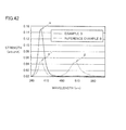
- In each of the semiconductor devices, the semiconductor layer may be made of silicon carbide of 4H type. In this case, when photoluminescence measurement is performed for the semiconductor layer at a room temperature (approximately 300K), a ratio of strength of a peak appearing in a wavelength of around 500 nm to strength of a peak appearing in a wavelength of around 390 nm is preferably 0.1 or smaller.
- According to review by the inventors, in the case where the semiconductor layer made of silicon carbide of 4H type (4H-SiC) is employed, it has been found that the on-resistance and the interface state density in the semiconductor device can be reduced by decreasing the peak appearing in the wavelength of around 500 nm in photoluminescence measurement under the room temperature. More specifically, it has been found that the peak in the wavelength of around 500 nm appears due to existence of certain stacking faults. Such stacking faults corresponding to this peak lead to increased on-resistance of the semiconductor device and increased interface state density in a MOS (Metal-Oxide-Semiconductor) structure. On the other hand, the peak appearing in the wavelength of around 390 nm corresponds to interband luminescence of the 4H-SiC. With the ratio of the peak strengths being not more than 0.1, the on-resistance and the interface state density in the semiconductor device can be reduced. Further, with the ratio of the peak strengths being not more than 0.01, the on-resistance and the interface state density in the semiconductor device can be further reduced. Here, the state in which the ratio of the peak strengths is not more than 0.1 or not more than 0.01 encompasses a case where the ratio of the peak strengths is 0. In other words, the peak in the wavelength of around 500 nm may not be appear. It is the most preferable that the peak in the wavelength of around 500 nm does not appear.
- A method for manufacturing a semiconductor device in one aspect of the present invention includes the steps of: preparing a substrate made of silicon carbide and having a main surface having an off angle of not less than -3° and not more than +5° relative to a (0-33-8) plane in a <01-10> direction; forming a semiconductor layer on the main surface of the substrate by means of epitaxial growth; forming an insulating film in contact with a surface of the semiconductor layer; and adjusting nitrogen atom concentration such that a maximum value of the nitrogen atom concentration becomes 1 × 1021 cm-3 or greater in a region within 10 nm from an interface between the semiconductor layer and the insulating film.
- Further, a method for manufacturing a semiconductor device in another aspect of the present invention includes the steps of: preparing a substrate made of silicon carbide and having a main surface having an off angle of not less than -3° and not more than +5° relative to a (0-33-8) plane in a <01-10> direction; forming a semiconductor layer on the main surface of the substrate by means of epitaxial growth; forming an insulating film in contact with a surface of the semiconductor layer; and adjusting hydrogen atom concentration such that a maximum value of the hydrogen atom concentration becomes 1 × 1021 cm-3 or greater in a region within 10 nm from an interface between the semiconductor layer and the insulating film.
- Further, a method for manufacturing a semiconductor device in still another aspect of the present invention includes the steps of: preparing a substrate made of silicon carbide and having a main surface having an off angle of not less than -3° and not more than +5° relative to a (0-33-8) plane in a <01-10> direction; forming a semiconductor layer on the main surface of the substrate by means of epitaxial growth; forming an insulating film in contact with a surface of the semiconductor layer; and adjusting total concentration of nitrogen atoms and hydrogen atoms such that a maximum value of the total concentration becomes 1 × 1021 cm-3 or greater in a region within 10 nm from an interface between the semiconductor layer and the insulating film.
- In this way, each of the semiconductor devices according to the present invention can be readily manufactured which has increased carrier mobility (channel mobility).
- The method for manufacturing the semiconductor device in the above-described one aspect may further include the step of providing hydrogen atoms in the region within 10 nm from the interface between the semiconductor layer and the insulating film. By providing both the nitrogen atoms and the hydrogen atoms in the vicinity of the interface between the semiconductor layer and the insulating film in this way, the carrier mobility can be increased more securely.
- In the method for manufacturing the semiconductor device in the above-described one aspect, the step of providing the hydrogen atoms may include the step of heating the substrate having the insulating film formed thereon, using gas containing hydrogen atoms as atmospheric gas.
- Further, in the method for manufacturing the semiconductor device in the above-described one aspect, the step of adjusting the nitrogen atom concentration may include the step of heating the substrate having the insulating film formed thereon, using gas containing nitrogen atoms as atmospheric gas.
- In this way, the hydrogen atoms and the nitrogen atoms can be readily introduced into the vicinity of the interface between the semiconductor layer and the insulating film.
- In the method for manufacturing the semiconductor device in the above-described one aspect, the step of adjusting the nitrogen atom concentration may include the step of heating the substrate using an inert gas as the atmospheric gas after the step of heating using the gas containing the nitrogen atoms as the atmospheric gas.
- Accordingly, the nitrogen atoms introduced in the vicinity of the interface between the semiconductor layer and the insulating film can more securely exhibit the effect of reducing the interface states.
- The method for manufacturing the semiconductor device in the above-described another aspect may further include the step of providing nitrogen atoms in the region within 10 nm from the interface between the semiconductor layer and the insulating film. By providing both the nitrogen atoms and the hydrogen atoms in the vicinity of the interface between the semiconductor layer and the insulating film in this way, the carrier mobility can be increased more securely.
- In the method for manufacturing the semiconductor device in the above-described another aspect, the step of providing the nitrogen atoms may include the step of heating the substrate having the insulating film formed thereon, using gas containing nitrogen atoms as atmospheric gas.
- Further, in the method for manufacturing the semiconductor device in the above-described another aspect, the step of adjusting the hydrogen atom concentration may include the step of heating the substrate having the insulating film formed thereon, using gas containing hydrogen atoms as the atmospheric gas.
- In this way, the hydrogen atoms and the nitrogen atoms can be readily introduced into the vicinity of the interface between the semiconductor layer and the insulating film.
- In the method for manufacturing the semiconductor device in the above-described another aspect, the step of adjusting the hydrogen atom concentration may include the step of heating the substrate using an inert gas as the atmospheric gas after the step of heating using the gas containing the hydrogen atoms as the atmospheric gas.
- Accordingly, the hydrogen atoms introduced in the vicinity of the interface between the semiconductor layer and the insulating film can more securely exhibit the effect of reducing the interface states.
- In the method for manufacturing the semiconductor device in each of the above-described one aspect and another aspect, the gas containing the hydrogen atoms may be water vapor or water vapor-containing oxygen. In this way, the hydrogen atoms can be readily introduced into the vicinity of the interface between the semiconductor layer and the insulating film.
- In the method for manufacturing the semiconductor device, the step of preparing the substrate may include the steps of: obtaining the substrate from a source material crystal made of silicon carbide of 4H type; and removing a processing damage layer formed in a region including the other main surface of the substrate thus obtained, the other main surface being opposite to the main surface of the substrate.
- As described above, the inventors have found that in the case where the semiconductor layer made of 4H-SiC is employed, the on-resistance and the interface state density in the semiconductor device can be reduced by reducing the peak strength in the wavelength of around 500 nm in the photoluminescence measurement under the room temperature. Further, as a result of more detailed review by the inventors, it has been found that in the case where the substrate is obtained from the source material crystal made of 4H-SiC and the semiconductor layer made of 4H-SiC is formed through epitaxial growth, the above-described peak strength is increased with the following mechanism to result in increased on-resistance in the semiconductor device.
- Specifically, when obtaining the substrate from the source material crystal, processing damage layers are formed in the vicinity of the main surfaces of the substrate. Of the two main surfaces of the substrate, the main surface (the main surface at the semiconductor layer side) on which the semiconductor layer is to be formed by means of epitaxial growth is thereafter smoothed with high precision by means of polishing or the like. As a result, the processing damage layer in the main surface at the semiconductor layer side is removed. In contrast, the processing damage layer remains in the vicinity of the main surface (main surface at the backside surface side) opposite to the side at which the semiconductor layer is formed. On the main surface at the semiconductor side, the semiconductor layer, the insulating film (oxide film), and the like are formed to fabricate the semiconductor device. In the process of manufacturing the semiconductor device, there are performed the step of heating to a temperature range of approximately 1000°C to approximately 1200°C such as thermal oxidation treatment, and the step of heating to a temperature range higher than the foregoing temperature range. Here, when the impurity concentration (for example, nitrogen concentration) is high in the substrate in order to reduce the resistivity of the substrate, stacking faults are generated from the processing damage layer remaining in the vicinity of the main surface at the backside surface side and grow in the substrate.
- On this occasion, the stacking faults grow in a <11-20> direction. Hence, when a general main surface close to a {0001} plane is employed as the main surface of the substrate for example, the stacking faults grow from the processing damage layer along the main surface at the backside surface. Hence, the stacking faults do not reach the main surface at the semiconductor layer side. Thus, the stacking faults are not propagated to the semiconductor layer formed on the main surface at the semiconductor layer side. However, when the main surface of the substrate at the semiconductor layer side corresponds to a plane close to the (0-33-8) plane as that of the semiconductor device of the present invention, the stacking faults grow from the processing damage layer to move away relative to the main surface at the backside surface side. Accordingly, the stacking faults reach the main surface at the semiconductor layer side. As a result, the stacking faults are propagated to the semiconductor layer formed on the main surface at the semiconductor layer side to result in strong peak strength in the wavelength of around 500 nm in the above-described photoluminescence measurement and result in increased on-resistance and interface state density in the semiconductor device.
- To address this, as described above, the step of preparing the substrate includes the step of removing the processing damage layer, whereby the propagation of the stacking faults to the semiconductor layer is suppressed. Accordingly, the on-resistance and the interface state density in the semiconductor device can be reduced.
- Preferably in the method for manufacturing the semiconductor device, in the step of obtaining the substrate, the substrate is obtained by slicing the source material crystal, and in the step of removing the processing damage layer, the processing damage layer formed in the substrate by slicing the source material crystal is removed.
- By slicing the source material crystal, the substrate can be readily obtained. Then, the processing damage layer formed in the substrate due to the slicing is removed, thereby suppressing the propagation of the stacking faults to the semiconductor layer. Accordingly, the on-resistance and the interface state density in the semiconductor device can be reduced.
- In the method for manufacturing the semiconductor device, in the step of removing the processing damage layer, the processing damage layer may be removed by means of fused KOH etching. Further, in the method for manufacturing the semiconductor device, in the step of removing the processing damage layer, the processing damage layer may be removed by means of dry etching. Further, in the method for manufacturing the semiconductor device, in the step of removing the processing damage layer, the processing damage layer may be removed by means of thermal etching. Further, in the method for manufacturing the semiconductor device, in the step of removing the processing damage layer, the processing damage layer may be removed by means of polishing. By means of the fused KOH etching, dry etching, thermal etching, polishing, or the like, the processing damage layer can be readily removed.
- As apparent from the description above, according to the semiconductor device and the method for manufacturing the semiconductor device in the present invention, there can be provided a semiconductor device excellent in electric characteristic such as channel mobility as well as a method for manufacturing such a semiconductor device.
-
-
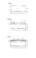
Fig. 1 is a schematic cross sectional view showing a structure of a semiconductor device. -
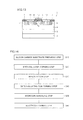
Fig. 2 is a flowchart for illustrating a method for manufacturing the semiconductor device shown inFig. 1 . -
Fig. 3 is a schematic cross sectional view for illustrating a step of the manufacturing method shown inFig. 2 . -
Fig. 4 is a schematic cross sectional view for illustrating a step of the manufacturing method shown inFig. 2 . -
Fig. 5 is a schematic cross sectional view for illustrating a step of the manufacturing method shown inFig. 2 . -
Fig. 6 is a schematic cross sectional view for illustrating a step of the manufacturing method shown inFig. 2 . -
Fig. 7 is a schematic cross sectional view for illustrating a step of the manufacturing method shown inFig. 2 . -
Fig. 8 is a schematic cross sectional view showing a structure of a semiconductor device in a second embodiment. -
Fig. 9 is a schematic cross sectional view for illustrating a method for manufacturing the semiconductor device shown inFig. 8 . -
Fig. 10 is a schematic cross sectional view for illustrating the method for manufacturing the semiconductor device shown inFig. 8 . -
Fig. 11 is a schematic cross sectional view for illustrating the method for manufacturing the semiconductor device shown inFig. 8 . -
Fig. 12 is a schematic cross sectional view for illustrating the method for manufacturing the semiconductor device shown inFig. 8 . -
Fig. 13 is a schematic cross sectional view showing a structure of a semiconductor device in a third embodiment. -
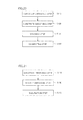
Fig. 14 is a flowchart for illustrating a method for manufacturing the semiconductor device shown inFig. 13 . -
Fig. 15 is a schematic cross sectional view showing a structure of a semiconductor device in a fourth embodiment. -
Fig. 16 is a flowchart for illustrating a method for manufacturing the semiconductor device shown inFig. 15 . -
Fig. 17 is a flowchart showing a variation of the method for manufacturing the semiconductor device inFig. 16 . -
Fig. 18 is a flowchart showing a second variation of the method for manufacturing the semiconductor device inFig. 16 . -
Fig. 19 is a schematic cross sectional view showing a structure of a silicon carbide substrate in a fifth embodiment. -
Fig. 20 is a flowchart schematically showing a method for manufacturing the silicon carbide substrate. -
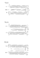
Fig. 21 is a flowchart schematically showing a method for manufacturing a silicon carbide substrate in a sixth embodiment. -
Fig. 22 is a schematic cross sectional view for illustrating the method for manufacturing the silicon carbide substrate in the sixth embodiment. -
Fig. 23 is a schematic cross sectional view for illustrating the method for manufacturing the silicon carbide substrate in the sixth embodiment. -
Fig. 24 is a schematic cross sectional view for illustrating the method for manufacturing the silicon carbide substrate in the sixth embodiment. -
Fig. 25 is a schematic cross sectional view showing a structure of a silicon carbide substrate in a seventh embodiment. -
Fig. 26 is a schematic cross sectional view showing a structure of a silicon carbide substrate in an eighth embodiment. -
Fig. 27 is a flowchart schematically showing a method for manufacturing the silicon carbide substrate in the eighth embodiment. -
Fig. 28 is a schematic cross sectional view showing a structure of a silicon carbide substrate in a ninth embodiment. -
Fig. 29 is a flowchart schematically showing a method for manufacturing the silicon carbide substrate in the ninth embodiment. -
Fig. 30 is a schematic cross sectional view showing a structure of a silicon carbide substrate in a tenth embodiment. -
Fig. 31 is a flowchart schematically showing a method for manufacturing the silicon carbide substrate in the tenth embodiment. -
Fig. 32 is a schematic cross sectional view for illustrating the method for manufacturing the silicon carbide substrate in the tenth embodiment. -
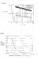
Fig. 33 is a graph showing a relation between channel mobility and a value of a peak of nitrogen atom concentration. -
Fig. 34 is a graph showing a relation between channel mobility and a value of a peak of total concentration of nitrogen atoms and hydrogen atoms. -
Fig. 35 is a schematic cross sectional view showing a semiconductor device prepared for measurement in an example 5. -
Fig. 36 is a graph showing a CV characteristic for a sample of an example A. -
Fig. 37 is a graph showing a CV characteristic for a sample of a comparative example A. -
Fig. 38 is a graph showing a CV characteristic of a sample of a reference example A. -
Fig. 39 is a graph showing a relation between an interface state density and energy with the conduction band regarded as a reference. -
Fig. 40 is a graph showing a relation between an interface state density and energy with the conduction band regarded as a reference. -
Fig. 41 is a graph showing a relation between an interface state density and a MOS channel mobility. -
Fig. 42 shows a result of photoluminescence measurement under a room temperature. - The following describes embodiments of the present invention with reference to figures. It should be noted that in the below-mentioned figures, the same or corresponding portions are given the same reference characters and are not described repeatedly.
- First, a first embodiment, which is one embodiment of the present invention, will be described. A
semiconductor device 1 shown inFig. 1 is a MOSFET of lateral type (Metal-Oxide-Semiconductor Field Effect Transistor) serving as the semiconductor device, and includes: asubstrate 2 made of silicon carbide (SiC) of 4H type; anepitaxial layer 3 formed on thissubstrate 2 and made of silicon carbide;a p type layer 4 formed on thisepitaxial layer 3 and made of silicon carbide; n+ regions 5,6 formed, with a space therebetween, in regions including the surface ofp type layer 4; anoxide film 8 located above a channel region between n+ regions 5, 6 and serving as a gate insulating film; agate electrode 10 formed on thisoxide film 8; and asource electrode 11 and adrain electrode 12 respectively formed on n+ regions 5, 6.Substrate 2 is a substrate having amain surface 2A located at the side ofepitaxial layer 3 serving as the semiconductor layer and corresponding to a (0-33-8) plane, which has an off angle of approximately 53° relative to a plane orientation of {0001}.Substrate 2 includes an n type impurity (impurity allowing substrate 2 to have n type conductivity such as nitrogen). -
Epitaxial layer 3 formed onsubstrate 2 and made of silicon carbide is an undoped layer.P type layer 4 provided on thisepitaxial layer 3 contains a p type impurity (impurity allowingp type layer 4 to have p type conductivity such as aluminum). Further, an n type impurity is implanted in each of n+ regions 5, 6. To coverp type layer 4 and n+ regions 5, 6,oxide films Oxide films source electrode 11 anddrain electrode 12 are formed which are respectively electrically connected to n+ regions 5, 6.Gate electrode 10 is disposed onoxide film 8 serving as a gate insulating film. A distance between n+ regions 5, 6, i.e., a channel length Lg can be set at, for example, approximately 100 µm. Further, a channel width can be, for example, twice as large as channel length Lg (approximately 200 µm). - In the semiconductor device shown in
Fig. 1 , the maximum value of the nitrogen atom concentration is equal to or greater than 1 × 1021 cm-3 in a region within 10 nm from an interface betweenoxide film 8 andp type layer 4 serving as the semiconductor layer. As a result, the channel region having channel length Lg (the region between n+ regions 5, 6 in p type layer 4) can be provided with mobility (channel mobility) of a sufficiently large value. - This is presumably due to the following reason. That is, in the case where
oxide film 8 is formed by means of thermal oxidation or the like, a multiplicity of interface states are formed at the interface betweenoxide film 8 andp type layer 4 serving as the semiconductor layer. Accordingly, without any modification, channel mobility in the channel region will be drastically decreased as compared with its theoretical value. To address this problem, nitrogen atoms are introduced between the interface region betweenoxide film 8 andp type layer 4 as described above, thereby achieving improved channel mobility while reducing the influence of the above-described interface states. - Further, in
semiconductor device 1 in the present embodiment,main surface 2A ofsubstrate 2 at theepitaxial layer 3 side corresponds to the (0-33-8) plane. Accordingly,p type layer 4, which is formed by means of epitaxial growth onmain surface 2A and impurity implantation, is provided with a main surface opposite tosubstrate 2 and corresponding to the (0-33-8) plane. As a result, the channel region (the region including the interface withoxide film 8 in n+ regions 5, 6 formed in p type layer 4) can be provided with a larger carrier mobility (channel mobility). - Referring to
Fig. 2-Fig. 7 , the following describes a method for manufacturing the semiconductor device in the first embodiment. First, as shown inFig. 2 , a silicon carbide substrate preparing step (S10) is performed. Prepared in this step assubstrate 2 is a silicon carbide substrate having n type conductivity and havingmain surface 2A corresponding to the plane with a plane orientation of (0-33-8). Such a substrate can be obtained by means of, for example, a technique of cutting an ingot (source material crystal) having a main surface corresponding to the (0001) plane, to obtain the substrate havingmain surface 2A exposed and corresponding to the (0-33-8). - Next, an epitaxial layer forming step (S20) is performed. Specifically, as shown in
Fig. 3 , undoped siliconcarbide epitaxial layer 3 is formed onsubstrate 2 by means of epitaxial growth. - Next, an implantation step (S30) is performed. Specifically, first, a p type impurity (for example, aluminum (Al)) is implanted into
epitaxial layer 3 to formp type layer 4 as shown inFig. 4 . Next, an n type impurity is implanted thereinto to form n+ regions 5, 6 as shown inFig. 5 . An exemplary, usable n type impurity is phosphorus (P). Any well-known method can be used to form n+ regions 5, 6. An example of the method is as follows. That is, an oxide film is formed to cover the upper surface ofp type layer 4 and is then provided, by means of photolithography and etching, with openings having the same planar shape pattern as that of the regions in which n+ regions 5, 6 are to be formed. Then, the n type impurity is implanted using, as a mask, the oxide film thus provided with this pattern. In this way, n+ regions 5, 6 described above can be formed. - Thereafter, activation annealing treatment is performed to activate the impurity thus implanted. This activation annealing treatment may be performed under conditions that, for example, heating temperature is set at 1700°C and heating time is set at 30 minutes.
- Next, a gate insulating film forming step (S40) is performed as shown in
Fig. 2 . Specifically,oxide film 7 serving as the gate insulating film is formed as shown inFig. 6 by oxidizing the upper surfaces ofp type layer 4 and n+ regions 5, 6.Oxide film 7 can have a thickness of, for example, 40 nm. - Next, a nitrogen annealing step (S50) is performed as shown in
Fig. 2 . Specifically, heat treatment is performed using nitrogen monoxide (NO) gas as atmospheric gas. This heat treatment can be performed under conditions that, for example, heating temperature is set at 1100°C and heating time is set at 1 hour. As a result, nitrogen atoms can be introduced into the interface region betweenoxide film 7 and each ofp type layer 4 and n+ regions 5, 6. Further, in this nitrogen annealing step, an annealing step using an inert gas may be performed after the annealing step using the atmospheric gas containing above-described nitrogen atoms. An example of the annealing step using an inert gas is an annealing step using argon (Ar) gas as the atmospheric gas. - Next, as shown in
Fig. 2 , an electrode forming step (S60) is performed. Specifically, a resist film having a pattern is formed onoxide film 7 by means of the photolithography method. By removing portions ofoxide film 7 using this resist film as a mask,openings 15 are formed in the regions located above n+ regions 5, 6. In each ofopenings 15, as shown inFig. 7 , a conductor film to be formed into each ofsource electrode 11 anddrain electrode 12 are formed. The conductor film is formed with the above-described resist film remaining thereon. Thereafter, a portion of the conductor film aboveoxide film 7 is removed (lifted off) together with the resist film by removing the resist film, thereby formingsource electrode 11 anddrain electrode 12 as shown inFig. 7 . On this occasion,oxide film 8 betweensource electrode 11 and drain electrode 12 (the portion ofoxide film 7 shown inFig. 6 ) is formed into the gate insulating film of the semiconductor device. - Thereafter, gate electrode 10 (see
Fig. 1 ) is formed onoxide film 8 serving as the gate insulating film. As a method of forminggate electrode 10, the following method can be used. For example, a resist film having an opening pattern at a region aboveoxide film 8 is formed in advance, and a conductor film to constitute the gate electrode is formed to cover the entire surface of the resist film. Then, by removing the resist film, portions of the conductor film other than the portion to be formed into the gate electrode are removed (lifted off). As a result, as shown inFig. 1 ,gate electrode 10 is formed. In this way,semiconductor device 1 shown inFig. 1 can be obtained. - Referring to
Fig. 8 , the following describes a semiconductor device in a second embodiment.Semiconductor device 1 in the present embodiment is a vertical type DiMOSFET (Double Implanted MOSFET), and includes: asubstrate 2, abuffer layer 21, a breakdownvoltage holding layer 22,p regions 23, n+ regions 24, p+ regions 25, anoxide film 26,source electrodes 11,upper source electrodes 27, agate electrode 10, and adrain electrode 12 formed on the backside surface ofsubstrate 2. Specifically,buffer layer 21, which is made of silicon carbide, is formed onmain surface 2A ofsubstrate 2 made of silicon carbide of n type conductivity.Buffer layer 21 has n type conductivity, and has a thickness of, for example, 0.5 µm. Further,buffer layer 21 can be adapted to contain an n type impurity at a concentration of, for example, 5 × 1017 cm-3. Formed onbuffer layer 21 is breakdownvoltage holding layer 22. Breakdownvoltage holding layer 22 is made of silicon carbide of n type conductivity, and has a thickness of 10 µm, for example. Further, breakdownvoltage holding layer 22 contains an n type impurity at a concentration of, for example, 5 × 1015 cm-3. - At a region including the main surface of breakdown
voltage holding layer 22 opposite tosubstrate 2,p regions 23 of p type conductivity are formed with a space interposed therebetween. In each ofp regions 23, n+ region 24 is formed at a region including the main surface ofp region 23. Further, at a location adjacent to n+ region 24, a p+ region 25 is formed.Oxide film 26 is formed to extend on n+ region 24 in onep region 23,p region 23, an exposed portion of breakdownvoltage holding layer 22 between the twop regions 23, theother p region 23, and n+ region 24 in theother p region 23. Onoxide film 26,gate electrode 10 is formed. Further,source electrodes 11 are formed on and in contact with n+ regions 24 and p+ regions 25. Onsource electrodes 11,upper source electrodes 27 are formed. Moreover,drain electrode 12 is formed on the main surface (backside surface) ofsubstrate 2 opposite to its main surface on whichbuffer layer 21 is formed. - Here, the maximum value of the nitrogen atom concentration is 1 × 1021 cm-3 or greater in a region within 10 nm from the interface between
oxide film 26 and the semiconductor layer, i.e., each of n+ regions 24, p+ regions 25,p regions 23, and breakdownvoltage holding layer 22. Accordingly, as withsemiconductor device 1 shown inFig. 1 , mobility can be improved particularly in the channel region below oxide film 26 (the portion of eachp region 23 making contact withoxide film 26 and located between n+ region 24 and breakdown voltage holding layer 22). - Further, in
semiconductor device 1 in the present embodiment,main surface 2A ofsubstrate 2 at thebuffer layer 21 side corresponds to the (0-33-8) plane. Hence, each ofp regions 23, which are formed by means of epitaxial growth onmain surface 2A and impurity implantation, has a main surface opposite tosubstrate 2 and corresponding to the (0-33-8) plane. As a result, carrier mobility (channel mobility) in the channel region can be further larger. - The following describes a method for manufacturing
semiconductor device 1 shown inFig. 8 , with reference toFig. 9-Fig. 12 . First, as with the method for manufacturing the semiconductor device as shown inFig. 2 , silicon carbide substrate preparing step (S10) is performed. In this step, as with the method for manufacturing the semiconductor device in the first embodiment, there is prepared substrate 2 (seeFig. 9 ) made of silicon carbide and having its main surface corresponding to the (0-33-8) plane. As substrate 2 (seeFig. 9 ), a substrate may be employed which has n type conductivity and has a substrate resistance of 0.02 Ωcm. - Next, epitaxial layer forming step (S20) is performed. Specifically,
buffer layer 21 is formed onmain surface 2A ofsubstrate 2. As the buffer layer, an epitaxial layer is formed which is made of silicon carbide of n type conductivity and has a thickness of 0.5 µm, for example.Buffer layer 21 has a conductive impurity at a concentration of, for example, 5 × 1017 cm-3. Then, onbuffer layer 21, breakdownvoltage holding layer 22 is formed as shown inFig. 9 . As breakdownvoltage holding layer 22, a layer made of silicon carbide of n type conductivity is formed using an epitaxial growth method. Breakdownvoltage holding layer 22 can have a thickness of, for example, 10 µm. Further, breakdownvoltage holding layer 22 includes an impurity of n type conductivity at a concentration of, for example, 5 × 1015 cm-3. - Next, as with the step shown in
Fig. 2 , implantation step (S30) is performed. Specifically, an impurity of p type conductivity is implanted into breakdownvoltage holding layer 22 using, as a mask, an oxide film formed through photolithography and etching, thereby formingp regions 23 as shown inFig. 10 . Further, after removing the oxide film thus used, an oxide film having a new pattern is formed through photolithography and etching. Using this oxide film as a mask, an n type impurity is implanted into predetermined regions to form n+ regions 24. In a similar way, an impurity of p type conductivity is implanted to form p+ regions 25. As a result, the structure shown inFig. 10 is obtained. - After such an implantation step, an activation annealing treatment is performed. This activation annealing treatment can be performed under conditions that, for example, argon gas is employed as atmospheric gas, heating temperature is set at 1700°C, and heating time is set at 30 minutes.
- Next, as with the step shown in
Fig. 2 , gate insulating film forming step (S40) is performed. Specifically, as shown inFig. 11 ,oxide film 26 is formed to cover breakdownvoltage holding layer 22,p regions 23, n+ regions 24, and p+ regions 25.Oxide film 26 may be formed by means of, for example, dry oxidation (thermal oxidation). The dry oxidation can be performed under conditions that heating temperature is set at 1200°C and heating time is set at 30 minutes. - Thereafter, as with the step shown in
Fig. 2 , nitrogen annealing step (S50) is performed. Specifically, an annealing treatment is performed in atmospheric gas of nitrogen monoxide (NO). Temperature conditions for this annealing treatment are, for example, as follows: heating temperature is 1100°C and heating time is 120 minutes. As a result, nitrogen atoms are introduced into a vicinity of the interface betweenoxide film 26 and each of breakdownvoltage holding layer 22,p regions 23, n+ regions 24, and p+ regions 25, which are disposed belowoxide film 26. Further, after the annealing step using the atmospheric gas of nitrogen monoxide, additional annealing may be performed using argon (Ar) gas, which is an inert gas. Specifically, using the atmospheric gas of argon gas, the additional annealing may be performed under conditions that heating temperature is set at 1100°C and heating time is set at 60 minutes. - Next, as with the step shown in
Fig. 2 , electrode forming step (S60) is performed. Specifically, a resist film having a pattern is formed onoxide film 26 by means of the photolithography method. Using the resist film as a mask, portions of the oxide film above n+ regions 24 and p+ regions 25 are removed by etching. Thereafter, a conductor film made of metal or the like is formed on the resist film, on the region making contact with n+ region 24 and p+ region 25 in each of the openings formed inoxide film 26, and on the main surface ofsubstrate 2 opposite to bufferlayer 21. Thereafter, the resist film is removed, thus removing (lifting off) the conductive film's portions located on the resist film. Here, as the conductor, nickel (Ni) can be used, for example. As a result, as shown inFig. 12 ,source electrodes 11 anddrain electrode 12 can be obtained. It should be noted that on this occasion, heat treatment for alloying is preferably performed. Specifically, using atmospheric gas of argon (Ar) gas, which is an inert gas, heat treatment (alloying treatment) is performed with heating temperature being set at 950°C and heating time being set at 2 minutes. Thereafter, onsource electrodes 11, upper source electrodes 27 (seeFig. 8 ) are formed. In this way, the semiconductor device shown inFig. 8 can be obtained. - Next, referring to
Fig. 13 , the following describes a semiconductor device in a third embodiment. Referring toFig. 13 ,semiconductor device 1 according to the present invention is configured basically the same assemiconductor device 1 shown inFig. 1 , but is different fromsemiconductor device 1 shown inFig. 1 in that the maximum value of hydrogen atom concentration is equal to or greater than 1 × 1021 cm- 3at aboundary region 41 including a region within 10 nm from the interface betweenoxide film 8 andp type layer 4 serving as the semiconductor layer. Also in this way, as with the semiconductor device shown inFig. 1 , mobility (channel mobility) in the channel region includingboundary region 41 can be sufficiently large in value. This is presumably due to the following reason. That is, insemiconductor device 1 shown inFig. 13 , the hydrogen atoms contained inboundary region 41 serve to reduce interface states in a manner similar to the nitrogen atoms contained in the region within 10 nm from the interface betweenp type layer 4 andoxide film 8 insemiconductor device 1 shown inFig. 1 . - Referring to
Fig. 14 , the following describes a method for manufacturing the semiconductor device in the third embodiment. The method for manufacturing the semiconductor device inFig. 14 is basically the same as the method for manufacturing the semiconductor device in theFig. 2 , but is different therefrom in that instead of nitrogen annealing step (S50) inFig. 2 , a hydrogen annealing step (S70) is performed. Specifically, as with the manufacturing method shown inFig. 2 , silicon carbide substrate preparing step (S10), epitaxial layer forming step (S20), implantation step (S30), and gate insulating film forming step (S40) are performed. Thereafter, hydrogen annealing step (S70) is performed. Specifically, heat treatment is performed using hydrogen gas (H2) as atmospheric gas. This heat treatment can be performed under conditions that, for example, heating temperature is set at 1100°C and heating time is set at 1 hour. As a result, the hydrogen atoms can be introduced into the interface region betweenoxide film 7 and each ofp type layer 4 and n+ regions 5, 6. Further, in this hydrogen annealing step, an annealing step using an inert gas may be performed after the annealing step using the atmospheric gas containing above-described hydrogen atoms. An example of the annealing step using an inert gas is an annealing step using argon (Ar) gas as the atmospheric gas. Further, in hydrogen annealing step (S70), water vapor or water vapor-containing oxygen gas may be used as the atmospheric gas instead of the hydrogen gas. - Thereafter, as with the manufacturing method shown in
Fig. 2 , electrode forming step (S60) is performed as shown inFig. 14 , thereby obtainingsemiconductor device 1 shown inFig. 13 . - Referring to
Fig. 15 , the following describes a semiconductor device in a fourth embodiment. Referring toFig. 15 ,semiconductor device 1 in the present embodiment is configured basically the same assemiconductor device 1 shown inFig. 1 , but is different fromsemiconductor device 1 shown inFig. 1 in that the maximum value of the total concentration of nitrogen atoms and hydrogen atoms is equal to or greater than 1 × 1021 cm-3 in aboundary region 51 including a region within 10 nm from the interface betweenoxide film 8 andp type layer 4 serving as the semiconductor layer. Also in this way, as with the semiconductor device shown inFig. 1 , mobility (channel mobility) in the channel region includingboundary region 41 can be sufficiently large in value. - Referring to
Fig. 16 , the following describes a method for manufacturingsemiconductor device 1 in the fourth embodiment. The method for manufacturing the semiconductor device inFig. 16 is basically the same as the method for manufacturing the semiconductor device in theFig. 2 , but is different therefrom in that hydrogen annealing step (S70) is performed after nitrogen annealing step (S50) inFig. 16 and before electrode forming step (S60). Specifically, as with the manufacturing method shown inFig. 2 , silicon carbide substrate preparing step (S10), epitaxial layer forming step (S20), implantation step (S30), gate insulating film forming step (S40), and nitrogen annealing step (S50) are performed. Thereafter, hydrogen annealing step (S70) is performed. This step (S70) can be performed under the same conditions (conditions of annealing using hydrogen gas) as that in hydrogen annealing step (S70) of the manufacturing method of the third embodiment. As a result, the nitrogen atoms and the hydrogen atoms can be introduced into the interface region betweenoxide film 7 and each ofp type layer 4 and n+ regions 5, 6. It should be noted that in hydrogen annealing step (S70), water vapor or water vapor-containing oxygen gas may be used as the atmospheric gas instead of the hydrogen gas. Further, hydrogen annealing step (S70) may be performed before nitrogen annealing step (S50). Furthermore, hydrogen annealing step (S70) and nitrogen annealing step (S50) may be performed simultaneously by performing heat treatment using atmospheric gas containing hydrogen atoms and nitrogen atoms. - Thereafter, as with the manufacturing method shown in
Fig. 2 , electrode forming step (S60) is performed as shown inFig. 16 , thereby obtainingsemiconductor device 1 shown inFig. 15 . - Referring to
Fig. 17 , the following describes a variation of the method for manufacturing the semiconductor device in the fourth embodiment. A method for manufacturing the semiconductor device inFig. 17 is basically the same as the method for manufacturing the semiconductor device inFig. 16 , but is different therefrom in that a post heat treatment step (S80) is performed after hydrogen annealing step (S70) inFig. 16 and before electrode forming step (S60). Specifically, as with the manufacturing method shown inFig. 16 , silicon carbide substrate preparing step (S10), epitaxial layer forming step (S20), implantation step (S30), gate insulating film forming step (S40), nitrogen annealing step (S50), and hydrogen annealing step (S70) are performed. Thereafter, post heat treatment step (S80) is performed. Specifically, an annealing step using an inert gas is performed. This annealing step can be performed under conditions that an inert gas (for example, argon (Ar)) is used as the atmospheric gas, heating temperature is set at 1100°C, and heating time is set at 60 minutes. The annealing step thus performed using the inert gas provides more securely the effect of reducing the interface states by means of the nitrogen atoms and hydrogen atoms introduced into the channel region in nitrogen annealing step (S50) and hydrogen annealing step (S70). - Thereafter, as with the manufacturing method shown in
Fig. 2 , electrode forming step (S60) is performed as shown inFig. 17 , thereby obtainingsemiconductor device 1 shown inFig. 15 . - It should be noted that a heat treatment step similar to the above-described post heat treatment step (S80) may be additionally performed between nitrogen annealing step (S50) and hydrogen annealing step (S70). Further, also in the manufacturing method shown in
Fig. 17 , hydrogen annealing step (S70) may be performed before nitrogen annealing step (S50), Furthermore, hydrogen annealing step (S70) and nitrogen annealing step (S50) may be performed simultaneously by performing heat treatment using atmospheric gas containing hydrogen atoms and nitrogen atoms. - Referring to
Fig. 18 , the following describes a second variation of the method for manufacturing the semiconductor device in the fourth embodiment. The method for manufacturing the semiconductor device inFig. 18 is basically the same as the method for manufacturing the semiconductor device inFig. 17 , but is different from the manufacturing method shown inFig. 17 in terms of the silicon carbide substrate preparing step. - Specifically, referring to
Fig. 18 , the silicon carbide substrate preparing step in the present variation includes: a source material crystal preparing step (S11); a slicing step (S12); and a processing damage layer removing step (S13). In step (S11), for example, a source material crystal made of silicon carbide of 4H type is fabricated by means of a sublimation method. In step (S12), the source material crystal thus fabricated in step (S11) is sliced to obtainsubstrate 2. In doing so, the source material crystal is sliced such thatsubstrate 2 will have one main surface corresponding to the (0-33-8) plane (plane at the carbon plane side) and will have the other main surface corresponding to the (03-38) plane (plane at the silicon plane side). - As a result of the slicing in step (S12), processing damage layers are formed in regions including both the main surfaces of
substrate 2. In step (S 13), at least the processing damage layer at the (03-38) plane side is removed. This processing damage layer can be removed by means of an etching process such as fused KOH etching, dry etching, or thermal etching, or by means of polishing, for example. On the other hand, the main surface at the (0-33-8) plane side, i.e., the main surface on which the epitaxial layer is to be formed in the subsequent step is smoothed to have a surface roughness suitable for epitaxial growth by means of a combination of mechanical polishing (MP), chemical mechanical polishing (CMP), and the like. As a result, the processing damage layer is also removed from the region including the main surface at the (0-33-8) plane side. It should be noted that as with the (03-38) plane side, the region including the main surface at the (0-33-8) plane side may be smoothed after removing the processing damage layer. - Thereafter, as shown in
Fig. 18 , as with the manufacturing method shown inFig. 17 , epitaxial layer forming step (S20), implantation step (S30), gate insulating film forming step (S40), nitrogen annealing step (S50), hydrogen annealing step (S70), post heat treatment step (S80), and electrode forming step (S60) are performed, thereby obtaining the semiconductor device of the second variation. - According to the manufacturing method in the second variation, the processing damage layer introduced in step (S12) into the region including the (03-38) plane in
substrate 2 is removed in step (S13). Further, the processing damage layer introduced into the region including the (0-33-8) plane insubstrate 2 is removed by the polishing process such as MP, CMP, or the like. Accordingly, stacking faults are suppressed from growing due to the processing damage layer in the process, such as gate insulating film forming step (S40), in which heating is performed at approximately 1000°C-1200°C. Accordingly, the stacking faults, which would otherwise cause deterioration of characteristics of the semiconductor device, (stacking faults corresponding to a peak in a wavelength of around 500 nm when photoluminescence measurement is performed under a room temperature) can be suppressed from being generated insubstrate 2 as well as inepitaxial layer 3 andp type layer 4 each serving as the semiconductor layer and formed onsubstrate 2 by means of epitaxial growth. As a result, according to the manufacturing method in the second variation, there can be manufactured asemiconductor device 1 in which a ratio of strength of a peak in a wavelength of around 500 nm to strength of a peak in a wavelength of around 390 nm is not more than 0.1 or not more than 0.01 when photoluminescence measurement is performed forepitaxial layer 3 andp type layer 4. In such asemiconductor device 1, the detrimental stacking faults corresponding to the peak in the wavelength of around 500 nm are suppressed from being generated in the semiconductor layer (epitaxial layer 3 and p type layer 4). This leads to improved characteristics ofsemiconductor device 1. - It should be noted that in each of the third and fourth embodiments, the lateral type MOSFET has been illustrated as
semiconductor device 1, but the feature of each of the third and fourth embodiments may be applied to the vertical type DiMOSFET shown inFig. 8 . Specifically, insemiconductor device 1 shown inFig. 8 , the maximum value of the hydrogen atom concentration or the maximum value of the total concentration of the nitrogen atoms and the hydrogen atoms may be 1 × 1021 cm-3 or greater in the region within 10 nm from the interface betweenoxide film 26 and each of the semiconductor layers, i.e., each of n+ regions 24, p+ regions 25,p regions 23, and breakdownvoltage holding layer 22. Further,main surface 2A ofsubstrate 2 at the semiconductor side can be adapted to correspond to the (0-33-8) plane. - Referring to
Fig. 19 , the following describes a semiconductor device in a fifth embodiment of the present invention. The semiconductor device in the present embodiment has basically the same structure and provides basically the same effect as those of the semiconductor device in each of the first to fourth embodiments. However, the semiconductor device in the present embodiment is different from that in each of the first to fourth embodiments in terms of a structure ofsubstrate 2. - Referring to
Fig. 19 ,substrate 2, which constitutessemiconductor device 1 in the present embodiment, includes: abase layer 110 made of silicon carbide; and aSiC layer 120 made of single-crystal silicon carbide and disposed on onemain surface 110A ofbase layer 110.Base layer 110 andSiC layer 120 are formed of different crystals.SiC layer 120 has a defect density smaller than that ofbase layer 110. - It is difficult for a high-quality silicon carbide single-crystal to have a large diameter. Meanwhile, for efficient manufacturing in a process of manufacturing a semiconductor device using a silicon carbide substrate, a substrate provided with predetermined uniform shape and size is required. Hence, even when a high-quality silicon carbide single-crystal (for example, silicon carbide single-crystal having a small defect density) is obtained, a region that cannot be processed into such a predetermined shape and the like by cutting, etc., may not be effectively used.
- To address this,
substrate 2 constituting the semiconductor device of the present embodiment includesbase layer 110 made of silicon carbide, andSiC layer 120 made of single-crystal silicon carbide and formed onbase layer 110, whereinSiC layer 120 has a defect density smaller than that ofbase layer 110. Thus,base substrate 110 formed of low-quality silicon carbide crystal having a large defect density is processed to have the above-described predetermined shape and size, thereby obtainingbase layer 110. On such abase layer 110, a high-quality silicon carbide single-crystal not shaped into the desired shape and the like is disposed asSiC layer 120.Substrate 2 thus obtained has the predetermined uniform shape and size, thus attaining effective manufacturing ofsemiconductor devices 1. Further, the silicon carbide substrate thus obtained utilizes such a high-quality SiC layer 120 to manufacture asemiconductor device 1, thereby effectively utilizing silicon carbide single-crystal. As a result, according to the semiconductor device of the present invention, there can be provided asemiconductor device 1 allowing for reduced manufacturing cost. - Further, the half width of X-ray rocking curve of
SiC layer 120 may be smaller than that ofbase layer 110. - Further,
base layer 110 may have an impurity concentration greater than 2 × 1019cm-3 whereasSiC layer 120 may have an impurity concentration greater than 5 × 1018cm-3 and smaller than 2 × 1019cm-3. - According to the study conducted by the inventors, when the impurity concentration is smaller than 2 × 1019 cm-3 in the substrate made of silicon carbide, generation of stacking faults resulting from heat treatment (for example, thermal oxidation treatment) in the process of manufacturing the semiconductor device can be suppressed, but when the impurity concentration exceeds 2 × 1019cm-3, it is difficult to suppress the stacking faults. Hence, when the impurity concentration exceeds 2 × 1019 cm-3, it is preferable to perform the step of removing a processing damage layer as in the second variation of the fourth embodiment.
- Meanwhile, generation of such stacking faults can be suppressed at least in
SiC layer 120 without removing the processing damage layer even when heat treatment is subsequently performed in the process of fabricating the device, by providingsubstrate 2 made of silicon carbide with a layer (base layer 110) having an impurity concentration greater than 2 × 1019cm-3 and having small resistivity; and disposing, onbase layer 110, a layer (SiC layer 120) having an impurity concentration smaller than 2 × 1019cm-3. Then, an epitaxial growth layer (active layer) made of SiC is formed on such aSiC layer 120 to fabricatesemiconductor device 1, thereby achieving reduced resistivity ofsilicon carbide substrate 2 due to the existence ofbase layer 110 and suppressing influence of stacking faults, which can be generated inbase layer 110, over the characteristics of the semiconductor device. Meanwhile, whenSiC layer 120 has an impurity concentration of 5 × 1018 cm-3 or smaller, the resistivity ofSiC layer 120 becomes too large. Accordingly,substrate 2 suitable for the vertical type semiconductor device shown inFig. 8 (semiconductor device in which current flows in the thickness direction of substrate 2) cannot be obtained, disadvantageously. - Thus, by setting the impurity concentration of
base layer 110 to be larger than 2 × 1019 cm-3 and setting the impurity concentration ofSiC layer 120 to be larger than 5 × 1018 cm-3 and smaller than 2 × 1019 cm-3, there can be obtainedsemiconductor device 1 capable of achieving reduced on-resistance while suppressing occurrence of stacking faults resulting from heat treatment in the process of fabricating the semiconductor device. - Here,
SiC layer 120 preferably has a micro pipe density smaller than that ofbase layer 110. Further,SiC layer 120 preferably has a threading screw dislocation density smaller than that ofbase layer 110. Further,SiC layer 120 preferably has a threading edge dislocation density smaller than that ofbase layer 110. Further,SiC layer 120 preferably has a basal plane dislocation density smaller than that ofbase layer 110. Further,SiC layer 120 preferably has a composite dislocation density smaller than that ofbase layer 110. Further,SiC layer 120 preferably has a stacking fault density smaller than that ofbase layer 110. Further,SiC layer 120 preferably has a point defect density smaller than that ofbase layer 110. - Thus, as compared with
base layer 110,SiC layer 120 has the reduced defect densities such as the micro pipe density, the threading screw dislocation density, the threading edge dislocation density, the basal plane dislocation density, the composite dislocation density, the stacking fault density, and the point defect density. Such aSiC layer 120 allows a high-quality active layer (epitaxial growth layer) to be formed onSiC layer 120. - Further,
base layer 110 andSiC layer 120 described above are connected to each other, for example. Accordingly,silicon carbide substrate 2 can be readily obtained in whichSiC layer 120 is provided while suppressing propagation of the defects ofbase layer 110. On this occasion,base layer 110 andSiC layer 120 may be directly connected to each other or may be connected to each other via an intermediate layer. - The following describes a method for manufacturing
substrate 2 in the present embodiment. Referring toFig. 20 , in the method for manufacturing the silicon carbide substrate in the present embodiment, the substrate preparing step is performed as step (S 110). In this step (S110), referring toFig. 19 ,base substrate 110 formed of single-crystal silicon carbide andSiC substrate 120 formed of single-crystal silicon carbide are prepared. -
SiC substrate 120 has amain surface 120A, which will be the main surface ofsubstrate 2 that will be obtained by this manufacturing method. Hence, on this occasion, the plane orientation ofmain surface 120A ofSiC substrate 120 is selected in accordance with desired plane orientation. Here, for example, aSiC substrate 120 having a main surface corresponding to the (0-33-8) plane is prepared. Meanwhile, a substrate having an impurity concentration greater than, for example, 2 × 1019 cm-3 is adopted asbase substrate 110. Further, forSiC substrate 120, a substrate is employed which has, for example, an impurity concentration greater than 5 × 1018cm-3 and smaller than 2 × 1019cm-3. - Next, a substrate smoothing step is performed as a step (S120). This step (S120) is not an essential step, but can be performed when the smoothness of
base substrate 110 and/orSiC substrate 120 prepared in step (S110) is insufficient. Specifically, for example, the main surface(s) ofbase substrate 110 and/orSiC substrate 120 are polished. On the other hand, by omitting this step, manufacturing cost can be reduced. Further, an etching process may be performed to remove a processing damage layer, which is formed in a region including a main surface ofSiC substrate 120 when obtainingSiC substrate 120 from a source material crystal (ingot). The etching process can be performed by means of, for example, fused KOH etching. - Next, as a step (S130), a stacking step is performed. In this step (S130), referring to
Fig. 19 ,base substrate 110 andSiC substrate 120 are stacked on each other such that theirmain surfaces - Next, as a step (S140), a connecting step is performed. In this step (S140),
base substrate 110 andSiC substrate 120 are connected to each other by, for example, heating the stacked substrate to fall within a range of temperatures equal to or greater than the sublimation temperature of silicon carbide. In this way, referring toFig. 19 ,substrate 2 includingbase layer 110 andSiC layer 120 is completed. Thissubstrate 2 is used in the method for manufacturing the semiconductor device in the present embodiment, andsemiconductor device 1 is manufactured in the same manner as those in the first to fourth embodiments. - Here, the heating temperature for the stacked substrate in step (S140) is preferably not less than 1800°C and not more than 2500°C. If the heating temperature is lower than 1800°C, it takes a long time to connect
base substrate 110 andSiC substrate 120, which results in decreased efficiency inmanufacturing substrate 2. On the other hand, if the heating temperature exceeds 2500°C, surfaces ofbase substrate 110 andSiC substrate 120 become rough, which may result in generation of a multiplicity of defects insubstrate 2 to be fabricated. In order to improve efficiency in manufacturing while restraining generation of defects insubstrate 2, the heating temperature for the stacked substrate in step (S140) is preferably set at not less than 1900°C and not more than 2100°C. Further, the pressure of atmosphere upon the heating in step (S140) is set at not less than 10-5 Pa and not more than 106 Pa, more preferably, not less than 10-2 Pa and not more than 104 Pa. In this way, the above-described connection can be achieved using a simple device. Further, the atmosphere upon the heating in step (S 140) is preferably inert gas atmosphere. More preferably, the atmosphere is inert gas atmosphere containing at least one selected from a group consisting of argon, helium, and nitrogen. - As a sixth embodiment, the following describes another method for manufacturing the substrate constituting the semiconductor device of the present invention, with reference to
Fig. 21 to Fig. 24 . The method for manufacturing the substrate in the sixth embodiment is performed in basically the same manner as that of the fifth embodiment. However, the method for manufacturing the substrate in the sixth embodiment is different from that of the fifth embodiment in terms of the process of formingbase layer 110. - Referring to
Fig. 21 , in the method for manufacturing the substrate in the sixth embodiment, the substrate preparing step is performed as step (S110). In this step (S110), referring toFig. 22 ,SiC substrate 120 is prepared as with that in the fifth embodiment and amaterial substrate 111 made of silicon carbide is prepared.Material substrate 111 may be made of single-crystal silicon carbide or polycrystal silicon carbide, or may be a sintered compact of silicon carbide. Further, instead ofmaterial substrate 111, material powder made of silicon carbide can be employed. - Next, as a step (S150), a closely arranging step is performed. In this step (S150), referring to
Fig. 22 ,SiC substrate 120 andmaterial substrate 111 are respectively held by afirst heater 181 and asecond heater 182 disposed face to face each other. In doing so,SiC substrate 120 andmaterial substrate 111 are disposed close to each other such that their main surfaces, i.e., amain surface 120B and a main surface 111A face each other with a space of not less than 1 µm and not more than 1 cm, for example, a space of approximately 1 mm interposed therebetween. - Next, as a step (S160), a sublimation step is performed. In this step (S160),
SiC substrate 120 is heated byfirst heater 181 to a predetermined substrate temperature. Further,material substrate 111 is heated to a predetermined material temperature bysecond heater 182. On this occasion,material substrate 111 is heated to reach the material temperature, thereby sublimating SiC from the surface of the material substrate. On the other hand, the substrate temperature is set lower than the material temperature. Specifically, for example, the substrate temperature is set lower than the source material temperature by not less than 1 °C and not more than 100°C. The substrate temperature is preferably 1800°C or greater and 2500°C or smaller, for example. Accordingly, as shown inFig. 23 , SiC sublimated frommaterial substrate 111 in the form of gas reaches the surface ofSiC substrate 120 and is accordingly solidified thereon, thereby formingbase layer 110. With this state being maintained, as shown inFig. 24 , all the SiC constitutingmaterial substrate 111 is sublimated and is transferred onto the surface ofSiC substrate 120. Accordingly, step (S160) is completed, thereby completingsubstrate 2 shown inFig. 19 . - The following describes yet another embodiment of the present invention, i.e., a seventh embodiment. A semiconductor device in the seventh embodiment has basically the same structure as that of the fifth embodiment. However, the semiconductor device of the seventh embodiment is different from that of the fifth embodiment in terms of its manufacturing method.
- Specifically, a substrate different in structure from that of the fifth embodiment is prepared in the silicon carbide substrate preparing step performed as step (S10) in the method for manufacturing the semiconductor device in the seventh embodiment. Referring to
Fig. 25 , insubstrate 2 prepared in the seventh embodiment, a plurality of SiC layers 120 are arranged side by side when viewed in a planar view. In other words, the plurality of SiC layers 120 are arranged alongmain surface 110A ofbase layer 110. More specifically, the plurality of SiC layers 120 are arranged in the form of a matrix onbase layer 110 such that adjacent SiC layers 120 are in contact with each other. Accordingly,substrate 2 of the present embodiment can be handled as asubstrate 2 having high-quality SiC layers 120 and a large diameter. Utilization of such asubstrate 2 allows for efficient manufacturing process of semiconductor devices. It should be noted thatsubstrate 2 in the seventh embodiment can be manufactured in a manner similar to that in the fifth embodiment or the sixth embodiment as follows. That is, in step (S130) of the fifth embodiment, a plurality ofSiC substrates 120 are arranged side by side when viewed in a planar view (seeFig. 19 ). Alternatively, in step (S 150) of the sixth embodiment, a plurality ofSiC substrates 120 are arranged side by side on and held by first heater 181 (seeFig. 22 ). - Further, in the method for manufacturing
semiconductor device 1 in the present embodiment,semiconductor device 1 is manufactured usingsubstrate 2 thus obtained. Here, by forming a semiconductor layer and the like onSiC layers 120 ofsubstrate 2 shown inFig. 25 , a plurality ofsemiconductor devices 1 arranged side by side when viewed in a planar view are fabricated. On this occasion, eachsemiconductor device 1 is fabricated so as not to extend across a boundary region between adjacent SiC layers 120. - The following describes still another embodiment of the present invention, i.e., an eighth embodiment.
Semiconductor device 1 in the eighth embodiment has basically the same structure and provides basically the same effects as those ofsemiconductor device 1 in the fifth embodiment. However,semiconductor device 1 in the eighth embodiment is different from that of the fifth embodiment in terms of structure ofsubstrate 2. - Namely, referring to
Fig. 26 , insubstrate 2 in the eighth embodiment, anamorphous SiC layer 140 is disposed betweenbase layer 110 andSiC layer 120 as an intermediate layer made of amorphous SiC. Then,base layer 110 andSiC layer 120 are connected to each other by thisamorphous SiC layer 140.Amorphous SiC layer 140 thus existing facilitates fabrication ofsubstrate 2 in whichbase layer 110 andSiC layer 120 different from each other in impurity concentration are stacked on each other. - The following describes a method for manufacturing
substrate 2 in the eighth embodiment. Referring toFig. 27 , in the method for manufacturingsubstrate 2 in the eighth embodiment, the substrate preparing step is performed as step (S110) in the same way as in the fifth embodiment, so as to preparebase substrate 110 andSiC substrate 120. - Next, as a step (S111), a Si layer forming step is performed. In this step (S111), a Si layer having a thickness of approximately 100 nm is formed on one main surface of
base substrate 110 prepared in step (S110), for example. This Si layer can be formed using a sputtering method, for example. - Next, the stacking step is performed as step (S130). In this step (S130),
SiC substrate 120 prepared in step (S110) is placed on the Si layer formed in step (S111). In this way, a stacked substrate is obtained in whichSiC substrate 120 is provided overbase substrate 110 with the Si layer interposed therebetween. - Next, as a step (S170), a heating step is performed. In this step (S170), the stacked substrate fabricated in step (S130) is heated, for example, in a mixed gas atmosphere of hydrogen gas and propane gas under a pressure of 1 × 10³ Pa at approximately 1500°C for 3 hours. Accordingly, the Si layer is supplied with carbon as a result of diffusion mainly from
base substrate 110 andSiC substrate 120, thereby formingamorphous SiC layer 140 as shown inFig. 26 . Accordingly,substrate 2 of the eighth embodiment can be readily manufactured in whichbase layer 110 andSiC layer 120 different from each other in impurity density are connected to each other byamorphous SiC layer 140, for example. - The following describes yet another embodiment of the present invention, i.e., a ninth embodiment. A
semiconductor device 1 in the ninth embodiment has basically the same structure and provides basically the same effects as those ofsemiconductor device 1 in the fifth embodiment. However,semiconductor device 1 in the ninth embodiment is different from that of the fifth embodiment in terms of structure ofsubstrate 2. - Specifically, referring to
Fig. 28 ,substrate 2 in the ninth embodiment is different from that of the fifth embodiment in that anohmic contact layer 150 serving as an intermediate layer is formed betweenbase layer 110 andSiC layer 120 by siliciding at least a portion of a metal layer. Further,base layer 110 andSiC layer 120 are connected to each other by thisohmic contact layer 150.Ohmic contact layer 150 thus existing facilitates fabrication ofsubstrate 2 in whichbase layer 110 andSiC layer 120 different in impurity concentration are stacked on each other, for example. - The following describes a method for manufacturing
substrate 2 in the ninth embodiment. Referring toFig. 29 , in the method for manufacturingsubstrate 2 in the ninth embodiment, the substrate preparing step is performed as step (S 110) as with that in the fifth embodiment to preparebase substrate 110 andSiC substrate 120. - Next, a metal film forming step is performed as a step (S112). In this step (S112), a metal film is formed by, for example, depositing a metal on one main surface of
base substrate 110 prepared in step (S110). This metal film includes, for example, at least one of metals forming silicide when being heated, such as nickel, molybdenum, titanium, aluminum, and tungsten. - Next, the stacking step is performed as step (S130). In this step (S130),
SiC substrate 120 prepared in step (S110) is placed on the metal film formed in step (S112). In this way, a stacked substrate is obtained in whichSiC substrate 120 is provided overbase substrate 110 with the metal film interposed therebetween. - Next, as step (S170), the heating step is performed. In this step (S170), the stacked substrate fabricated in step (S130) is heated to approximately 1000°C in an inert gas atmosphere such as argon, for example. In this way, at least a portion of the metal film (a region thereof making contact with
base substrate 110 and a region thereof making contact with the SiC substrate) is silicided to formohmic contact layer 150 making ohmic contact withbase layer 110 andSiC layer 120. As a result,substrate 2 of the ninth embodiment can be readily manufactured in whichbase layer 110 andSiC layer 120 different in impurity concentration are connected to each other byohmic contact layer 150, for example. - The following describes yet another embodiment of the present invention, i.e., a tenth embodiment. A
semiconductor device 1 in the tenth embodiment has basically the same structure and provides basically the same effects as those ofsemiconductor device 1 in the fifth embodiment. However,semiconductor device 1 in the tenth embodiment is different from that of the fifth embodiment in terms of structure ofsubstrate 2. - Specifically, referring to
Fig. 30 ,substrate 2 of the tenth embodiment is different from that of the fifth embodiment in that acarbon layer 160 is formed betweenbase layer 110 andSiC layer 120 as an intermediate layer. Then,base layer 110 andSiC layer 120 are connected to each other by thiscarbon layer 160.Carbon layer 160 thus existing facilitates fabrication ofsubstrate 2 in whichbase layer 110 andSiC layer 120 different in impurity concentration are stacked on each other, for example. - The following describes a method for manufacturing
substrate 2 in the tenth embodiment. Referring toFig. 31 , first, step (S110) is performed in the same way as in the fifth embodiment, and then step (S 120) is performed as required in the same way as in the fifth embodiment. - Next, as a step (S125), an adhesive agent applying step is performed. In this step (S 125), referring to
Fig. 32 , for example, a carbon adhesive agent is applied to the main surface ofbase substrate 110, thereby forming aprecursor layer 161. The carbon adhesive agent can be formed of, for example, a resin, graphite particles, and a solvent. Here, an exemplary resin usable is a resin formed into non-graphitizable carbon by heating, such as a phenol resin. An exemplary solvent usable is phenol, formaldehyde, ethanol, or the like. Further, the carbon adhesive agent is preferably applied at an amount of not less than 10 mg/cm2 and not more than 40 mg/cm2, more preferably, at an amount of not less than 20 mg/cm2 and not more than 30 mg/cm2. Further, the carbon adhesive agent applied preferably has a thickness of not more than 100 µm, more preferably, not more than 50 µm. - Next, the stacking step is performed as step (S 130). In this step (S130), referring to
Fig. 32 ,SiC substrate 120 is placed on and in contact withprecursor layer 161 formed on and in contact with the main surface ofbase substrate 110, thereby fabricating a stacked substrate. - Next, as a step (S180), a prebake step is performed. In this step (S180), the stacked substrate is heated, thereby removing the solvent component from the carbon adhesive agent constituting
precursor layer 161. Specifically, for example, while applying a load to the stacked substrate in the thickness direction thereof, the stacked substrate is gradually heated to fall within a range of temperature exceeding the boiling point of the solvent component. Preferably, this heating is performed withbase substrate 110 andSiC substrate 120 being pressed against each other using a clamp or the like. Further, by performing the prebaking (heating) as long as possible, the adhesive agent is degassed to improve strength in adhesion. - Next, as a step (S190), a firing step is performed. In this step (S190), the stacked substrate with
precursor layer 161 heated and accordingly prebaked in step (S180) is heated to a high temperature, preferably, not less than 900°C and not more than 1100°C, for example, 1000°C for preferably not less than 10 minutes and not more than 10 hours, for example, for 1 hour, thereby firingprecursor layer 161. Atmosphere employed upon the firing can be an inert gas atmosphere such as argon. The pressure of the atmosphere can be, for example, atmospheric pressure. In this way,precursor layer 161 is formed intocarbon layer 160 made of carbon. As a result, referring toFig. 30 ,substrate 2 of the tenth embodiment is obtained in which base substrate (base layer) 10 and SiC substrate (SiC layer) 20 are connected to each other bycarbon layer 160. - Here, the following describes characteristic configurations of the present invention although some of them have been already described in the embodiments above.
-
Semiconductor device 1 according to the present invention includes:substrate 2 made of silicon carbide and having a main surface having an off angle of not less than - 3° and not more than +5° relative to the (0-33-8) plane in the <01-10> direction; the semiconductor layer (p type layer 4 ofFig. 1 ,p region 23 ofFig. 8 ); and the insulating film (oxide film 8 ofFig. 1 ,oxide film 26 ofFig. 8 ). The semiconductor layer (p type layer 4, p region 23) is formed onsubstrate 2 and is made of silicon carbide. The insulating film (oxide film 8, 26) is formed in contact with the surface of the semiconductor layer (p type layer 4,p region 23 including the channel region). The maximum value of nitrogen atom concentration is 1 × 1021 cm-3 or greater in the region within 10 nm from the interface between the semiconductor layer and the insulating film (the interface between the channel region andoxide film 8, 26). - In this way, carrier mobility (channel mobility) can be made larger in the channel region in the vicinity of the interface between
oxide film semiconductor device 1 can be obtained which is excellent in electric characteristic and exhibits a sufficiently large channel mobility. It should be noted that the maximum value of the nitrogen atom concentration is set at 1 × 1021cm-3 or greater as described above because the channel mobility can be 50 cm2/Vs or greater, which is a practically sufficient value, by setting the nitrogen atom concentration at the above-described value or greater. - In
semiconductor device 1, hydrogen atoms may be contained in the region within 10 nm from the interface between the semiconductor layer (p type layer 4 ofFig. 1 ,p region 23 ofFig. 8 ) and the insulating film (oxide film 8, 26). In this case, interface states in this region can be reduced more securely. -
Semiconductor device 1 according to the present invention includes:substrate 2 made of silicon carbide and having a main surface having an off angle of not less than - 3° and not more than +5° relative to the (0-3 3-8) plane in the <01-10> direction; the semiconductor layer (p type layer 4 ofFig. 13 ,p region 23 ofFig. 8 ); and the insulating film (oxide film 8 ofFig. 13 ,oxide film 26 ofFig. 8 ). The semiconductor layer (p type layer 4, p region 23) is formed onsubstrate 2 and is made of silicon carbide. The insulating film (oxide film 8, 26) is formed in contact with the surface of the semiconductor layer (p type layer 4,p region 23 including the channel region). The maximum value of hydrogen atom concentration is 1 × 1021 cm-3 or greater in the region within 10 nm from the interface between the semiconductor layer and the insulating film (for example, the interface, included inboundary region 41 ofFig. 13 , between the channel region andoxide film 8, 26). - In this way, carrier mobility can be made larger in the channel region in the vicinity of the interface between
oxide film - In
semiconductor device 1, nitrogen atoms may be contained in the region within 10 nm from the interface between the semiconductor layer (p type layer 4 ofFig. 13 ,p region 23 ofFig. 8 ) and the insulating film (oxide film 8 ofFig. 13 ,oxide film 26 ofFig. 8 ). In this case, interface states in this region can be reduced more securely. -
Semiconductor device 1 according to the present invention includes:substrate 2 made of silicon carbide and having a main surface having an off angle of not less than - 3° and not more than +5° relative to the (0-33-8) plane in the <01-10> direction; the semiconductor layer (p type layer 4 ofFig. 15 ,p region 23 ofFig. 8 ); and the insulating film (oxide film 8 ofFig. 15 ,oxide film 26 ofFig. 8 ). The semiconductor layer (p type layer 4, p region 23) is formed onsubstrate 2 and is made of silicon carbide. The insulating film (oxide film 8, 26) is formed in contact with the surface of the semiconductor layer (p type layer 4,p region 23 including the channel region). The maximum value of the total concentration of the nitrogen atoms and the hydrogen atoms is 1 × 1021 cm-3 or greater in the region within 10 nm from the interface between the semiconductor layer and the insulating film (for example, the interface, included inboundary region 51 ofFig. 15 , between the channel region andoxide film 8, 26). - In this way, carrier mobility can be made larger in the channel region in the vicinity of the interface between
oxide film - Further,
semiconductor device 1 described above includessubstrate 2 made of silicon carbide and having the main surface having an off angle of not less than -3° and not more than +5° relative to the (0-33-8) plane in the <01-10> direction. More preferably, the main surface ofsubstrate 2 has a plane orientation of substantially (0-33-8), further preferably, the main surface of the substrate has a plane orientation of (0-33-8). Here, the expression "the main surface of the substrate has a plane orientation of substantially (0-33-8)" is intended to encompass a case where the plane orientation of the main surface of the substrate is included in a range of off angle such that the plane orientation can be substantially regarded as (0-33-8) in consideration of processing accuracy of the substrate and the like. In this case, the range of off angle is, for example, a range of off angle of ±2° relative to (0-33-8). In this case, the above-described carrier mobility (channel mobility) can be the maximum. - It should be noted that the off angle is set at not less than -3° and not more than +5° relative to the (0-33-8) plane in the <01-10> direction because an experiment conducted by the inventors has revealed that the range of off angle allowing for particularly good carrier mobility (channel mobility) is at least the above-described range.
- In
semiconductor device 1, it is preferable that the interface state density in a level lower than the conduction band by 0.1 eV is smaller than 1 × 1012cm-2eV-1. In this case, with the above-described interface state density, the carrier mobility of the channel region can become sufficiently large. It should be noted that in the case where the interface state density is greater than 1 × 1012cm-2eV-1, the channel mobility insemiconductor device 1 falls below 50 cm2/Vs, which is considered as a practically sufficient value. Hence, the value of the interface state density is preferably smaller than 1 × 1012cm-2eV-1. - Performed in the method for manufacturing the semiconductor device in the present invention is the step (substrate preparing step (S10)) of preparing
substrate 2 made of silicon carbide and having its main surface having an off angle of not less than -3° and not more than +5° relative to the (0-33-8) plane in the <01-10> direction. Performed next is the step (epitaxial layer forming step (S20)) of forming the semiconductor layer onsubstrate 2. Performed thereafter is the step (gate insulating film forming step (S40)) of forming the insulating film in contact with the surface of the semiconductor layer. Performed thereafter is the step (nitrogen annealing step (S50)) of adjusting the nitrogen atom concentration such that the maximum value of the nitrogen atom concentration becomes 1 × 1021 cm-3 or greater in the region within 10 nm from the interface between the semiconductor layer and the insulating film. In this way,semiconductor device 1 according to the present invention can be readily manufactured which has increased carrier mobility (channel mobility). - The method for manufacturing the semiconductor device may further include the step (for example, hydrogen annealing step (S70) of
Fig. 16 orFig. 17 ) of providing hydrogen atoms in the region within 10 nm from the interface between the semiconductor layer (p type layer 4, p region 23) and the insulating film (oxide film 8, 26). In this case, the semiconductor device can be readily manufactured which contains the hydrogen atoms in addition to the nitrogen atoms in the above-described region. - In the method for manufacturing the semiconductor device, the step (hydrogen annealing step (S70)) of providing the hydrogen atoms includes the step of heating the substrate having the insulating film (
oxide film 8, 26) formed thereon, using gas containing hydrogen atoms as atmospheric gas. In this case, the hydrogen atom concentration can be readily adjusted in the vicinity of the interface between the semiconductor layer (p type layer 4,p region 23 including the channel region) andoxide film - In the method for manufacturing the semiconductor device, the step (hydrogen annealing step (S70)) of providing the hydrogen atoms may include the step of heating the substrate using an inert gas as atmospheric gas after the step of heating using the gas containing the hydrogen atoms as the atmospheric gas. In this case, the carrier mobility of
semiconductor device 1 can be further increased. - In the method for manufacturing the semiconductor device, nitrogen annealing step (S50) may include the step of
heating substrate 2 having the insulating film (oxide film 8, 26) formed thereon, using gas containing nitrogen atoms as atmospheric gas. In this case, the nitrogen atom concentration can be readily adjusted in the vicinity of the interface between the semiconductor layer (p type layer 4,p region 23 including the channel region) andoxide film - In the method for manufacturing the semiconductor device, nitrogen annealing step (S50) may include the step of
heating substrate 2 using an inert gas (Ar gas) as the atmospheric gas, after the step of heating using the gas containing the nitrogen atoms as the atmospheric gas. In this case, the carrier mobility ofsemiconductor device 1 can be further increased. - Performed first in the method for manufacturing the semiconductor device in the present invention is the step (silicon carbide substrate preparing step (S10)) of preparing
substrate 2 made of silicon carbide and having its main surface having an off angle of not less than -3° and not more than +5° relative to the (0-33-8) plane in the <01-10> direction. Next, the step (epitaxial layer forming step (S20)) of forming the semiconductor layer onsubstrate 2 is performed. Then, the step (gate insulating film forming step (S40)) of forming the insulating film in contact with the surface of the semiconductor layer is performed. Performed thereafter is the step (hydrogen annealing step (S70)) of adjusting the hydrogen atom concentration such that the maximum value of the hydrogen atom concentration becomes 1 × 1021 cm-3 or greater in the region within 10 nm from the interface between the semiconductor layer and the insulating film. In this way,semiconductor device 1 according to the present invention can be readily manufactured which has increased carrier mobility (channel mobility). - The method for manufacturing the semiconductor device may further include the step (nitrogen annealing step (S50)) of providing the nitrogen atoms in the region within 10 nm from the interface between the semiconductor layer (
p type layer 4, p region 23) and the insulating film (oxide film 8, 26). In this case, the semiconductor device can be readily manufactured which contains the nitrogen atoms in addition to the hydrogen atoms in the above-described region. - In the method for manufacturing the semiconductor device, the step (nitrogen annealing step (S50)) of providing the nitrogen atoms may include the step of heating the substrate having the insulating film (
oxide film 8, 26) formed thereon, using gas containing nitrogen atoms as atmospheric gas. In this case, the nitrogen atom concentration can be readily adjusted in the vicinity of the interface between the semiconductor layer (p type layer 4,p region 23 including the channel region) andoxide film - In the method for manufacturing the semiconductor device, the step (nitrogen annealing step (S50)) of providing the nitrogen atoms may include the step of heating the substrate using an inert gas as the atmospheric gas, after the step of heating using the gas containing the nitrogen atoms as the atmospheric gas. In this case, the carrier mobility of
semiconductor device 1 can be further increased. - In the method for manufacturing the semiconductor device, the step (hydrogen annealing step (S70)) of adjusting the hydrogen atom concentration may include the step of heating the substrate having the insulating film (
oxide film 8, 26) formed thereon, using the gas containing the hydrogen atoms as the atmospheric gas. In this case, the hydrogen atom concentration can be readily adjusted in the vicinity of the interface between the semiconductor layer (p type layer 4,p region 23 including the channel region) andoxide film - In the method for manufacturing the semiconductor device, the step (hydrogen annealing step (S70)) of adjusting the hydrogen atom concentration may include the step of heating the substrate using an inert gas as the atmospheric gas, after the step of heating using the gas containing the hydrogen atoms as the atmospheric gas. In this case, the carrier mobility of
semiconductor device 1 can be further increased. - In the method for manufacturing the semiconductor device, the gas containing the hydrogen atoms may be water vapor or water vapor-containing oxygen gas. In this case, the water vapor, which is readily available and readily handled, is used as the atmospheric gas. Accordingly, hydrogen annealing step (S70) described above can be performed relatively readily.
- Performed first in the method for manufacturing the semiconductor device in the present invention is the step (silicon carbide substrate preparing step (S10)) of preparing
substrate 2 made of silicon carbide and having its main surface having an off angle of not less than -3° and not more than +5° relative to the (0-33-8) plane in the <01-10> direction. Next, the step (epitaxial layer forming step (S20)) of forming the semiconductor layer onsubstrate 2 is performed. Performed next is the step (gate insulating film forming step (S40)) of forming the insulating film in contact with the surface of the semiconductor layer. Performed thereafter is the step (nitrogen annealing step (S50) and hydrogen annealing step (S70)) of adjusting the total concentration of the nitrogen atoms and the hydrogen atoms such that the maximum value of the total concentration thereof becomes 1 × 1021 cm-3 or greater in the region within 10 nm from the interface between the semiconductor layer and the insulating film. In this way,semiconductor device 1 according to the present invention can be readily manufactured which has increased carrier mobility (channel mobility). - The following describes an experiment conducted to confirm the effect of the present invention.
- Semiconductor devices each having the structure shown in
Fig. 1 were fabricated as samples in the following manner. That is, anepitaxial layer 3 having a thickness of 10 µm was formed on an n typesilicon carbide substrate 2 having a thickness of 400 µm. Onepitaxial layer 3,a p type layer 4 having a thickness of 1 µm was formed. Then, phosphorus (P) was implanted thereinto as an n type impurity for n+ regions 5, 6. As the impurity concentration, a value of 1 × 1020cm-3 was employed. Further, a gate length (channel length Lg), which was a distance between n+ regions 5, 6, was set at 100 µm. Further, a gate width (channel width) was set at 200 µm. - Then, an oxide film was formed by means of dry oxidation treatment, and then nitrogen annealing was performed. In this way, a sample was fabricated. Another sample was also fabricated by forming the oxide film, then performing the nitrogen annealing, and then performing annealing treatment (argon annealing treatment) using argon gas, which was an inert gas, as atmosphere. Here, the dry oxidation treatment for forming
oxide film 8 was performed under conditions that heating temperature was set at 1200°C and heating time was set at 30 minutes. The oxide film thus formed had a thickness of 33-46 nm. Further, in the nitrogen annealing step, nitrogen monoxide gas was used as the atmospheric gas, heating temperature was set at 1100°C, and heating time was set at 60 minutes. Further, the sample to be subjected to the argon annealing treatment underwent the nitrogen annealing step under conditions that nitrogen monoxide gas was used as the atmospheric gas, heating temperature was set at 1100°C, and heating time was set at 120 minutes. The argon annealing treatment was performed under conditions that argon gas was used as the atmospheric gas, heating temperature was set at 1100°C, and heating time was set at 60 minutes. Still another sample was also fabricated which had not been through the nitrogen annealing step after the formation of the gate insulating film. - Then, as with the manufacturing method in the first embodiment, as shown in
Fig. 1 , asource electrode 11 and adrain electrode 12 were formed. Then, agate electrode 10 was formed onoxide film 8 serving as the gate insulating film. Each ofsource electrode 11 anddrain electrode 12 was made of nickel (Ni) and had a thickness of 0.1 µm.Gate electrode 10 was made of aluminum (Al) and had a thickness of 1 µm. - Next, channel mobility of each of the above-described samples was measured. As a measurement method, the following method was employed. That is, with source-drain voltage VDS = 0.1 V, gate voltage VG was applied and source-drain current IDS was measured (gate voltage dependency was measured). Then, with gm = (δIDS)/(δVG), the maximum value of the channel mobility with respect to the gate voltage was calculated in accordance with the following formula:

where L represents the gate length, d represents the thickness of the oxide film, W represents the gate width, and ε represents the dielectric constant of the oxide film. - A result of the measurement for the mobility in the channel is shown in
Fig. 33 . InFig. 33 , the horizontal axis represents the peak value (peak concentration of the nitrogen atoms) of the nitrogen atom concentration measured in each of the samples, whereas the vertical axis represents the measured channel mobility (MOS channel mobility) of the semiconductor device. - As shown in
Fig. 33 , the MOS channel mobility was increased as the peak concentration of nitrogen was higher. Here, the minimally required channel mobility to achieve a lower on-resistance than that of a conventional MOSFET which adopts silicon as its source material is considered to be approximately 50 cm2/Vs. Hence, referring toFig. 33 , with the peak concentration of the nitrogen atoms being set at 1 × 10²¹CM-3 or greater, it is considered that channel mobility of a sufficient value can be achieved. - The following describes an experiment conducted to confirm the effect attained when hydrogen atoms are provided in a region within 10 nm from an interface between a semiconductor layer and an insulating film.
- Semiconductor devices each having the structure shown in
Fig. 1 were fabricated as samples in the following manner. That is, anepitaxial layer 3 having a thickness of 10 µm was formed on an n typesilicon carbide substrate 2 having a thickness of 400 µm. Onepitaxial layer 3,a p type layer 4 having a thickness of 1 µm was formed. Next, phosphorus (P) was implanted thereinto as an n type impurity for n+ regions 5, 6. The concentration of this impurity was set at 1 × 1020 cm-3. Further, a gate length (channel length Lg), which was a distance between n+ regions 5, 6, was set at 100 µm. Further, a gate width (channel width) was set at 200 µm. - Then, an oxide film was formed by means of dry oxidation treatment, and then hydrogen annealing was performed. In this way, a sample was fabricated. Another sample was also fabricated by forming the oxide film, then performing the hydrogen annealing, and then performing annealing treatment (argon annealing treatment) using argon gas, which was an inert gas, as atmosphere. Here, the dry oxidation treatment for forming
oxide film 8 was performed under conditions that heating temperature was set at 1200°C and heating time was set at 30 minutes. The oxide film thus formed had a thickness of 33-45 nm. Further, in the hydrogen annealing step, hydrogen gas was used as the atmospheric gas, heating temperature was set at 1100°C, and heating time was set at 60 minutes. Further, the sample to be subjected to the argon annealing treatment underwent the hydrogen annealing under conditions that hydrogen gas was used as the atmospheric gas, heating temperature was set at 1100°C, and heating time was set at 120 minutes. In the argon annealing treatment, argon gas was used as the atmospheric gas, heating temperature was set at 1100°C, and heating time was set at 60 minutes. Still another sample was also fabricated which had not been through the hydrogen annealing step after the formation of the gate insulating film. - After the formation of the insulating film described above, as with the manufacturing method in the first embodiment of the present invention, as shown in
Fig. 1 , asource electrode 11 and adrain electrode 12 were formed. Then, agate electrode 10 was formed onoxide film 8 serving as the gate insulating film. Each ofsource electrode 11 anddrain electrode 12 was made of nickel (Ni) and had a thickness of 0.1 µm.Gate electrode 10 was made of aluminum (Al) and had a thickness of 1 µm. - Next, channel mobility of each of the above-described samples was measured. For the measurement method, the same method as that used in the experiment of example 1 was employed.
- A result of the measurement of the mobility in the channel showed a relation similar to the relation illustrated above and shown in
Fig. 33 , i.e., the relation between the peak value of the nitrogen atom concentration and the channel mobility. In other words, as with the case ofFig. 33 , the MOS channel mobility was increased as the peak concentration of nitrogen was higher. Now, an approximation line is drawn in the graph to approximate the data indicating the relation between the peak concentration of the hydrogen atoms and the channel mobility. This approximation line is substantially the same curve as the approximation line (curve) in the graph ofFig. 33 . Here, the minimally required channel mobility to achieve a lower on-resistance than that of a conventional MOSFET which adopts silicon as its source material is considered to be approximately 50 cm2/Vs. Hence, with the peak concentration of the hydrogen atoms being set at 1 × 1021 cm-3 or greater, it is considered that channel mobility of a sufficient value can be achieved. - The following describes an experiment in which water vapor was used as atmospheric gas in heat treatment to provide hydrogen atoms in a region within 10 nm from an interface between a semiconductor layer and an insulating film.
- Semiconductor devices each having the structure shown in
Fig. 1 were fabricated as samples. The method of fabricating the samples was basically the same as the method of fabricating the samples in example 2. That is, anepitaxial layer 3 having a thickness of 10 µm was formed on n typesilicon carbide substrate 2 having a thickness of 400 µm. Onepitaxial layer 3,a p type layer 4 having a thickness of 1 µm was formed. Next, phosphorus (P) was implanted thereinto as an n type impurity for n+ regions 5, 6. The impurity concentration was set at 1 × 1020 cm-3 Further, a gate length (channel length Lg), which was a distance between n+ regions 5, 6, was set at 100 µm. Further, a gate width (channel width) was set at 200 µm. - Then, an oxide film was formed by means of dry oxidation treatment, and then water vapor-containing oxygen gas annealing was performed. In this way, a sample was fabricated. Another sample was also fabricated by forming the oxide film, then performing the water vapor-containing oxygen gas annealing, and then performing annealing treatment (argon annealing treatment) using argon gas, which was an inert gas, as atmosphere. Here, the dry oxidation treatment for forming
oxide film 8 was performed under conditions that heating temperature was set at 1200°C and heating time was set at 30 minutes. The oxide film thus formed had a thickness of 33-44 nm. Further, in the water vapor-containing oxygen gas annealing step, water vapor-containing oxygen gas was used as the atmospheric gas, heating temperature was set at 1100°C, and heating time was set at 60 minutes. Further, the sample to be subjected to the argon annealing treatment underwent the water vapor-containing oxygen gas annealing under conditions that water vapor-containing oxygen gas was used as the atmospheric gas, heating temperature was set at 1100°C, and heating time was set at 120 minutes. The argon annealing treatment was performed under conditions that argon gas was used as the atmospheric gas, heating temperature was set at 1100°C, and heating time was set at 60 minutes. Still another sample was also fabricated which had not been through the water vapor-containing oxygen gas annealing step after the formation of the gate insulating film. - After the formation of the insulating film described above, as with the manufacturing method in the first embodiment of the present invention, as shown in
Fig. 1 , asource electrode 11 and adrain electrode 12 were formed. Then, agate electrode 10 was formed onoxide film 8 serving as the gate insulating film. Each ofsource electrode 11 anddrain electrode 12 was made of nickel (Ni) and had a thickness of 0.1 µm.Gate electrode 10 was made of aluminum (Al) and had a thickness of 1 µm. - Next, channel mobility of each of the above-described samples was measured. For the measurement method, the same method as that used in the experiment of example 1 was employed.
- A result of the measurement of the mobility in the channel showed a relation similar to the relation illustrated above and shown in
Fig. 33 , i.e., the relation between the peak value of the nitrogen atom concentration and the channel mobility. In other words, as with the case ofFig. 33 , the MOS channel mobility was increased as the peak concentration of hydrogen was higher. Now, an approximation line is drawn in the graph to approximate the data indicating the relation between the peak concentration of the hydrogen atoms and the channel mobility. This approximation line is substantially the same curve as the approximation line (curve) in the graph ofFig. 33 . Here, the minimally required channel mobility to achieve a lower on-resistance than that of a conventional MOSFET which adopts silicon as its source material is considered to be approximately 50 cm2/Vs. Hence, with the peak concentration of the hydrogen atoms being set at 1 × 1021 cm-3 or greater, it is considered that channel mobility of a sufficient value can be achieved. - Next, the following describes an experiment in which gas containing nitrogen atoms and hydrogen atoms was employed as atmospheric gas in heat treatment to provide nitrogen atoms and hydrogen atoms in a region within 10 nm from an interface between a semiconductor layer and an insulating film.
- Semiconductor devices each having the structure shown in
Fig. 1 were fabricated as samples. The method of fabricating the samples was basically the same as the method of fabricating the samples in example 2. That is, anepitaxial layer 3 having a thickness of 10 µm was formed on n typesilicon carbide substrate 2 having a thickness of 400 µm. Onepitaxial layer 3,a p type layer 4 having a thickness of 1 µm was formed. Next, phosphorus (P) was implanted thereinto as an impurity having n type conductivity for n+ regions 5, 6. The impurity concentration was set at 1 × 1020 cm-3. Further, a gate length (channel length Lg), which was a distance between n+ regions 5, 6, was set at 100 µm. Further, a gate width (channel width) was set at 200 µm. - Then, an oxide film was formed by means of dry oxidation treatment, and then nitrogen annealing was performed. In this way, a sample was fabricated. Another sample was also fabricated by forming the gate insulating film, then performing the nitrogen annealing, and then performing hydrogen annealing. Here, the dry oxidation treatment for forming
oxide film 8 was performed under conditions that heating temperature was set at 1200°C and heating time was set at 30 minutes. The oxide film thus formed had a thickness of 33-45 nm. Further, in the nitrogen annealing step, nitrogen monoxide (NO) gas was used as the atmospheric gas, heating temperature was set at 1100°C, and heating time was set at 20 minutes or 60 minutes. Further, in the hydrogen annealing treatment, hydrogen gas was used as the atmospheric gas, heating temperature was set at 1100°C, and heating time was set at 30 minutes. Still another sample was also fabricated which had not been through the nitrogen annealing step and the hydrogen step after the formation of the gate insulating film. - After the formation of the insulating film described above, as with the manufacturing method in the first embodiment of the present invention, as shown in
Fig. 1 , asource electrode 11 and adrain electrode 12 were formed in each of the samples. Then, agate electrode 10 was formed onoxide film 8 serving as the gate insulating film. Each ofsource electrode 11 anddrain electrode 12 was made of nickel (Ni) and had a thickness of 0.1 µm.Gate electrode 10 was made of aluminum (Al) and had a thickness of 1 µm. - Next, channel mobility of each of the above-described samples was measured. For the measurement method, the same method as that used in the experiment of example 1 was employed.
- A result of the measurement of the mobility in the channel showed a relation similar to the relation illustrated above and shown in
Fig. 33 , i.e., the relation between the peak value of the nitrogen atom concentration and the channel mobility. The result of the measurement for the mobility in the channel is shown inFig. 34 . InFig. 34 , the horizontal axis represents the peak value (peak concentration of the total of nitrogen and hydrogen) of the total concentration of the nitrogen atoms and hydrogen atoms measured in each of the samples, whereas the vertical axis represents the measured channel mobility (MOS channel mobility) of the semiconductor device. - As shown in
Fig. 34 , the MOS channel mobility was increased as the peak concentration of the total of nitrogen and hydrogen was higher. Here, the minimally required channel mobility to achieve a lower on-resistance than that of a conventional MOSFET which adopts silicon as its source material is considered to be approximately 50 cm2/Vs. Hence, referring toFig. 34 , with the peak value of the total concentration of the nitrogen atoms and the hydrogen atoms being set at 1 × 1021 cm-3 or greater, it is considered that channel mobility of a sufficient value can be achieved. - To confirm the effect of the present invention, semiconductor devices were fabricated and interface states at an interface between a semiconductor layer and an insulating film in each of the semiconductor devices was evaluated.
-
Fig. 35 is a schematic cross sectional view showing a semiconductor device prepared for measurement in example 5. The semiconductor device shown inFig. 35 was a MOS capacitor and included: asubstrate 2 that was an n type silicon carbide substrate; abuffer layer 21 formed onsubstrate 2; a breakdownvoltage holding layer 22 formed onbuffer layer 21; anoxide film 26 formed on breakdownvoltage holding layer 22; agate electrode 10 formed on the oxide film; and abackside electrode 31 formed on the backside surface of substrate 2 (the main surface thereof opposite to its surface on whichbuffer layer 21 was formed). - The semiconductor device was manufactured through the following steps.
First, an ingot (source material crystal) of 4H-SiC was sliced to obtainsubstrate 2 having a thickness of 400 µm. In doing so,substrate 2 was obtained such that one main surface ofsubstrate 2 would correspond to the (0-33-8) plane (plane of the carbon plane side) and the other main surface thereof would correspond to the (03-38) plane (plane of the silicon plane side). Next, fused KOH etching was performed to remove a processing damage layer formed, during the slicing, in a region including a main surface. The fused KOH etching was performed under conditions that temperature was set at 520°C and time was set at 10 minutes. Next, the main surface at the (0-33-8) plane side was polished. This polishing is performed by sequentially performing LAP (lapping), MP (mechanical polishing), and CMP (chemical mechanical polishing). - Next, on the polished main surface at the (0-33-8) plane side,
buffer layer 21 and breakdownvoltage holding layer 22 were formed by means of epitaxial growth. Further,oxide film 26 was formed on breakdownvoltage holding layer 22 by means of thermal oxidation, and thengate electrode 10 andbackside electrode 31 were formed, thereby obtaining the MOS capacitor shown inFig. 35 (example A). - Meanwhile, for comparison, a MOS capacitor (comparative example A) was also fabricated in a process similar to that for example A but in the process, the main surface (the other main surface) at the (03-38) plane side was polished instead of the main surface at the (0-33-8) plane side,
buffer layer 21, breakdownvoltage holding layer 22,oxide film 26, andgate electrode 10 were formed on the other main surface, andbackside electrode 31 was formed on the above-described one main surface. - In addition, a MOS capacitor (reference example A) was also fabricated in a process similar to that for example A but in the process, the processing damage layer was not removed by means of the fused KOH etching.
- The capacitance-voltage characteristic (CV characteristic) of each of the samples of example A, comparative example A, and reference example A, each of which had the configuration of the semiconductor device (MOS capacitor) shown in
Fig. 35 , was measured. It should be noted that high frequency CV measurement was performed at a measurement frequency of 1 MHz. Meanwhile, low frequency CV measurement was performed using a Quasistatic CV measurement method. It should be noted that capacitance Cs, which resulted from a depletion layer formed at the semiconductor side of the MOS interface, was calculated by solving Poisson equation. In doing so, inversion state was not taken into consideration and deep depletion state was assumed. - Further, interface state density of each of the samples of example A and comparative example A was calculated using a High-Low method. The following describes gist of the method of calculating the interface state density using the High-Low method.
- In the high frequency CV measurement, capacitance Cit relatively large in emission time constant and resulting from interface states does not appear as a capacitance component. On the other hand, in the CV measurement (low frequency CV measurement) obtained at a low frequency at which electrons can be captured to and emitted from the interface states, the capacitance is observed as a value obtained by adding capacitance resulting from the interface states to the capacitance in the high frequency CV measurement. Here, the capacitance obtained by the low frequency CV measurement includes information of oxide film capacitance, depletion layer capacitance, and interface state capacitance. Hence, capacitance CLF obtained by the low frequency CV measurement is expressed by the following formula (1):

- However, in the high frequency CV measurement, the interface state capacitance is not responded (is not detected). Hence, capacitance CHF obtained by the high frequency CV measurement is expressed by the following Formula (2):

- Accordingly, from the above-described formulae (1), (2), the following Formula (3) is obtained:

- From Formula (3), interface state density Dit can be calculated.
- Referring to
Fig. 36-Fig. 39 , results of the above-described measurements will be described. It should be noted thatFig. 39 is a graph showing a relation between the interface state density calculated from the CV characteristic shown in each ofFig. 36 and Fig. 37 and energy with the conduction band regarded as a reference. - In the graph of each of
Fig. 36-Fig. 38 , the horizontal axis represents voltage and the vertical axis represents the capacitance. It should be noted that the capacitance represented by the vertical axis is shown with the entire capacitance C being normalized by oxide film capacitance Cox. As apparent fromFig. 36-Fig. 38 , in the sample of example A of the present invention inFig. 36 , there was no large difference between the high frequency CV characteristic and the low frequency CV characteristic. In contrast, in each of the samples of comparative example A shown inFig. 37 and reference example A shown inFig. 38 , there was a relatively large difference between the high frequency CV characteristic and the low frequency CV characteristic. This is presumably because influence of the capacitance (interface state capacitance) resulting from the interface states became larger in the samples of comparative example A and reference example A than that in the sample of the example. - Furthermore,
Fig. 39 shows results of calculating the respective interface state densities of the samples of example A and comparative example A by means of the above-described High-Low method. InFig. 39 , the vertical axis represents the interface state density, whereas the horizontal axis represents a value of energy with the conduction band regarded as a reference. - As apparent from
Fig. 39 , the sample of example A (sample in whichbuffer layer 21, breakdownvoltage holding layer 22,oxide film 26, andgate electrode 10 are formed on the (0-33-8) plane) has a lower interface state density in any energy level than that of the sample of comparative example A (sample in whichbuffer layer 21, breakdownvoltage holding layer 22,oxide film 26, andgate electrode 10 are formed on the (03-38) plane). Further, also in an energy level lower than the conduction band by 0.1eV, it can be determined that the interface state density of the sample of example A is smaller than 1 × 1012 cm-2eV-1. - From this, it was confirmed that by employing the structure in which the semiconductor layer and the insulating film are formed particularly on the (0-33-8) plane that is a plane of the carbon plane side of the {03-38} plane, the interface state density in the semiconductor device can be reduced as compared with a case of employing a structure in which the semiconductor layer and the insulating film are formed on the (03-38) plane of the silicon plane side.
- Likewise, the interface state density of the sample of reference example A was also calculated using the High-Low method (see
Fig. 38 ), and was plotted in a graph ofFig. 40 together with the result of calculation for example A (seeFig. 36 ). Referring toFig. 40 , the sample of example A (sample from which the processing damage layer had been removed) had a lower interface state density in any energy level than that of the sample of reference example A (sample from which the processing damage layer had not been removed). - From this, it was confirmed that the interface state density in the semiconductor device can be reduced by removing the processing damage layer formed in the backside surface of the substrate.
- To confirm the effect of the present invention, a relation between interface state density and MOS channel mobility was evaluated in fabricated samples.
- Semiconductor devices each having the structure shown in
Fig. 1 were fabricated as samples in the following manner. That is, anepitaxial layer 3 having a thickness of 10 µm was formed on n typesilicon carbide substrate 2 having a thickness of 400 µm. Onepitaxial layer 3,a p type layer 4 having a thickness of 1 µm was formed. Next, phosphorus (P) was implanted thereinto as an impurity of n type conductivity for n+ regions 5, 6. The impurity concentration was set at 1 × 1020 cm-3. Further, a gate length (channel length Lg), which was a distance between n+ regions 5, 6, was set at 100 µm. Further, a gate width (channel width) was set at 200 µm. - Then, an oxide film was formed by means of dry oxidation treatment, and then nitrogen annealing was performed. In this way, a sample was fabricated. In the nitrogen annealing step, NO gas was used as the atmospheric gas, heating temperature was set at 1100°C, and heating time was set at 60 minutes. Another sample was also fabricated by forming the oxide film, then performing the nitrogen annealing, and then performing annealing treatment (argon annealing treatment) using argon gas, which was an inert gas, as atmosphere. The nitrogen annealing step was performed under conditions that NO gas was used as the atmospheric gas, heating temperature was set at 1100°C, and heating time was set at 120 minutes. In the argon annealing treatment, argon gas was used as the atmospheric gas, heating temperature was set at 1100°C, and heating time was set at 60 minutes. Here, the dry oxidation treatment for forming
oxide film 8 was performed under common conditions that heating temperature was set at 1200°C and heating time was set at 30 minutes. Still another sample was also fabricated which had not been through the nitrogen annealing step after the formation of the gate insulating film. It should be noted that in each of the samples, the oxide film thus formed had a thickness of 33-46 nm. - After the formation of the insulating film described above, as with the manufacturing method in the first embodiment of the present invention, as shown in
Fig. 1 , asource electrode 11 and adrain electrode 12 were formed. Then, agate electrode 10 was formed onoxide film 8 serving as the gate insulating film. Each ofsource electrode 11 anddrain electrode 12 was made of nickel (Ni) and had a thickness of 0.1 µm.Gate electrode 10 was made of aluminum (Al) and had a thickness of 1 µm. - Next, channel mobility of each of the above-described samples of the semiconductor devices thus fabricated was measured. For the measurement method, the same method as that used in the experiment of example 1 was employed.
- Further, the interface state density was calculated in each of the samples using the same method as the method used in the experiment of example 5 (i.e., using the High-Low method based on data of the high frequency CV characteristic and the low frequency CV characteristic.
- A result of the measurement was shown in
Fig. 41 . InFig. 41 , the horizontal axis represents a value of the interface state density in an energy level lower than the conduction band by 0.1 eV. On the other hand, inFig. 41 , the vertical axis represents the measured channel mobility (MOS channel mobility) of the semiconductor device. - As apparent from
Fig. 41 , as the interface state density is lower, the channel mobility is larger. Here, the minimally required value for the channel mobility to achieve a lower on-resistance than that of a conventional MOSFET which adopts silicon as its source material is considered to be approximately 50 em2/Vs as described above. InFig. 41 , it can be seen that a range of the interface state density allowing the channel mobility to be 50 cm2/Vs is a range of 7 × 1011 cm-2eV-1 or smaller. However, in view of a fact that a large error may be generally introduced into the measured value of the interface state density, it is considered that based on the experience of the inventors, sufficient channel mobility can be attained by setting the interface state density (in the level lower than the conduction band by 0.1eV) to be smaller than 1 × 1012cm-2eV-1. - An experiment was conducted to inspect why the on-resistance of the semiconductor device was reduced by removing the processing damage layer from the backside surface of the substrate. The experiment was conducted in the following procedure.
- First, an ingot (source material crystal) of 4H-SiC was sliced to obtain a substrate. This substrate was subjected to fused KOH etching to remove a processing damage layer formed, during the slicing, in a region including its main surface. The fused KOH etching was performed under conditions that temperature was set at 520°C and time was set at 10 minutes. Next, the one main surface is polished. This polishing is performed by sequentially performing LAP (lapping), MP (mechanical polishing), and CMP (chemical mechanical polishing). Next, on the one main surface thus polished, an epitaxial growth layer was formed. Further, an oxide film was formed on the epitaxial growth layer by means of thermal oxidation. The thermal oxidation was performed under conditions of 1200°C and 120 minutes (example B). On the other hand, for comparison, a sample (reference example B) was also fabricated which had the processing damage layer remaining in the backside surface because the fused KOH etching was not performed in the above-described procedure. Then, the substrate of each of the samples of example B and comparative example B was removed by polishing from the backside surface of the substrate (the main surface thereof opposite to the side at which the epitaxial growth layer was formed), and the epitaxial growth layer exposed accordingly was subjected to photoluminescence measurement under a room temperature. The measurement was performed in the following manner using He-Cd laser (wavelength of 325 nm) as excitation laser. That is, the laser was converged by a lens to irradiate the sample therewith. Then, photoluminescence generated from each of the samples was converged by the lens and then passed through a filter or the like to come into a spectrometer for wavelength dispersion. Then, photoluminescence spectrum was obtained using a CCD (Charge Coupled Device) or the like, The wavelength resolution thereof was 1 nm.
-
Fig. 42 shows results of the photoluminescence measurement. InFig. 42 , the horizontal axis represents wavelength, whereas the vertical axis represents strength. As shown inFig. 42 , in the sample of example B, it can be seen that a peak appears in a wavelength of around 390 nm (peak α, which is a peak corresponding to interband luminescence). No peak is confirmed in a wavelength of around 500 nm. On the other hand, in the sample of reference example B, a peak (peak α') in the wavelength of around 390 nm has a strength reduced as compared with that in example B. Further, a distinctive peak (peak β) appears in the wavelength of around 500 nm. It can be concluded that stacking faults corresponding to the peak in around 500 nm cause increase of the on-resistance and the interface state density in the semiconductor device, based on the above-described result and the inventors' experiment result that on-resistance and interface state density in a semiconductor device can be reduced by decreasing a ratio of peak strength in the wavelength of around 500 nm to peak strength in the wavelength of around 390 nm (by decreasing the ratio to not more than 0.1, preferably, not more than 0.01). It was confirmed that by decreasing the ratio (to not more than 0.1, preferably, not more than 0.01), the on-resistance and the interface state density can be reduced in the semiconductor device. - It should be noted that the MOSFET has been illustrated in the above-described embodiments as one example of the semiconductor device of the present invention, but the semiconductor device of the present invention is not limited to this and may be a semiconductor device in another form, such as an IGBT (Insulated Gate Bipolar Transistor).
- The embodiments and examples disclosed herein are illustrative and non-restrictive in any respect. The scope of the present invention is defined by the terms of the claims, rather than the embodiments described above, and is intended to include any modifications within the scope and meaning equivalent to the terms of the claims,
- The semiconductor device and the method for manufacturing the semiconductor device in the present invention are particularly advantageously applicable to a semiconductor device, which is required to achieve improved channel mobility, as well as a method for manufacturing such a semiconductor device.
- 1: semiconductor device; 2: substrate; 2A: main surface; 3: epitaxial layer; 4: p type layer; 5, 6: n+ region; 7, 8: oxide film; 10: gate electrode; 11: source electrode; 12: drain electrode; 15: opening; 21: buffer layer; 22: breakdown voltage holding layer; 23: p region; 24: n+ region; 25: p+ region 26: oxide film; 27: upper source electrode; 31: backside electrode; 41, 51; boundary region; 110: base layer (base substrate); 110A: main surface; 111: material substrate; 111A: main surface; 120: SiC layer (SiC substrate); 120A, 120B: main surface; 140: amorphous SiC layer; 150: ohmic contact layer; 160: carbon layer; 161: precursor layer; 181: first heater; 182: second heater.
Claims (22)
- A semiconductor device (1) comprising:a substrate (2) made of silicon carbide and having a main surface (2A) having an off angle of not less than -3° and not more than +5° relative to a (0-33-8) plane in a <01-10> direction;a semiconductor layer (4) made of silicon carbide and formed on said main surface (2A) of said substrate (2) by means of epitaxial growth; andan insulating film (8) formed in contact with a surface of said semiconductor layer (4),a maximum value of nitrogen atom concentration being 1 × 1021 cm-3 or greater in a region within 10 nm from an interface between said semiconductor layer (4) and said insulating film (8).
- The semiconductor device (1) according to claim 1, wherein hydrogen atoms are contained in said region within 10 nm from the interface between said semiconductor layer (4) and said insulating film (8).
- The semiconductor device (1) according to claim 1, wherein an interface state density is smaller than 1 × 1012 cm-2eV-1 in a level smaller than a conduction band by 0.1 eV.
- The semiconductor device (1) according to claim 1, wherein:said semiconductor layer (4) is made of silicon carbide of 4H type, andwhen photoluminescence measurement is performed for said semiconductor layer (4), a ratio of strength of a peak appearing in a wavelength of around 500 nm to strength of a peak appearing in a wavelength of around 390 nm is 0.1 or smaller.
- A semiconductor device (1) comprising:a substrate (2) made of silicon carbide and having a main surface (2A) having an off angle of not less than -3° and not more than +5° relative to a (0-33-8) plane in a <01-10> direction;a semiconductor layer (4) made of silicon carbide and formed on said main surface (2A) of said substrate (2) by means of epitaxial growth; andan insulating film (8) formed in contact with a surface of said semiconductor layer (4),a maximum value of hydrogen atom concentration being 1 × 1021 cm-3 or greater in a region within 10 nm from an interface between said semiconductor layer (4) and said insulating film (8).
- The semiconductor device (1) according to claim 5, wherein nitrogen atoms are contained in said region within 10 nm from the interface between said semiconductor layer (4) and said insulating film (8).
- A semiconductor device (1) comprising:a substrate (2) made of silicon carbide and having a main surface (2A) having an off angle of not less than -3° and not more than +5° relative to a (0-33-8) plane in a <01-10> direction;a semiconductor layer (4) made of silicon carbide and formed on said main surface (2A) of said substrate (2) by means of epitaxial growth; andan insulating film (8) formed in contact with a surface of said semiconductor layer (4),a maximum value of total concentration of nitrogen atoms and hydrogen atoms being 1 × 1021 cm-3 or greater in a region within 10 nm from an interface between said semiconductor layer (4) and said insulating film (8).
- A method for manufacturing a semiconductor device (1) comprising the steps of:preparing a substrate (2) made of silicon carbide and having a main surface (2A) having an off angle of not less than -3° and not more than +5° relative to a (0-33-8) plane in a <01-10> direction;forming a semiconductor layer (4) on said main surface (2A) of said substrate (2) by means of epitaxial growth;forming an insulating film (8) in contact with a surface of said semiconductor layer (4); andadjusting nitrogen atom concentration such that a maximum value of the nitrogen atom concentration becomes 1 × 1021 cm-3 or greater in a region within 10 nm from an interface between said semiconductor layer (4) and said insulating film (8).
- The method for manufacturing the semiconductor device (1) according to claim 8, further comprising the step of providing hydrogen atoms in said region within 10 nm from the interface between said semiconductor layer (4) and said insulating film (8).
- The method for manufacturing the semiconductor device (1) according to claim 9, wherein the step of providing said hydrogen atoms includes the step of heating said substrate (2) having said insulating film (8) formed thereon, using gas containing hydrogen atoms as atmospheric gas.
- The method for manufacturing the semiconductor device (1) according to claim 10, wherein said gas containing hydrogen atoms is water vapor or water vapor-containing oxygen.
- The method for manufacturing the semiconductor device (1) according to claim 8, wherein the step of adjusting said nitrogen atom concentration includes the step of heating said substrate (2) having said insulating film (8) formed thereon, using gas containing nitrogen atoms as atmospheric gas.
- The method for manufacturing the semiconductor device (1) according to claim 12, wherein the step of adjusting said nitrogen atom concentration includes the step of heating said substrate (2) using an inert gas as the atmospheric gas after the step of heating using said gas containing nitrogen atoms as the atmospheric gas.
- The method for manufacturing the semiconductor device (1) according to claim 8, wherein:the step of preparing said substrate (2) includes the steps of
obtaining said substrate (2) from a source material crystal made of silicon carbide of 4H type, and
removing a processing damage layer formed in a region including the other main surface of said substrate (2) thus obtained, the other main surface being opposite to said main surface (2A) of said substrate (2). - The method for manufacturing the semiconductor device (1) according to claim 14, wherein;in the step of obtaining said substrate (2), said substrate (2) is obtained by slicing said source material crystal, andin the step of removing said processing damage layer, said processing damage layer formed in said substrate (2) by slicing said source material crystal is removed.
- The method for manufacturing the semiconductor device (1) according to claim 14, wherein in the step of removing said processing damage layer, said processing damage layer is removed by means of fused KOH etching.
- The method for manufacturing the semiconductor device (1) according to claim 14, wherein in the step of removing said processing damage layer, said processing damage layer is removed by means of dry etching.
- The method for manufacturing the semiconductor device (1) according to claim 14, wherein in the step of removing said processing damage layer, said processing damage layer is removed by means of thermal etching.
- The method for manufacturing the semiconductor device (1) according to claim 14, wherein in the step of removing said processing damage layer, said processing damage layer is removed by means of polishing.
- A method for manufacturing a semiconductor device (1) comprising the steps of:preparing a substrate (2) made of silicon carbide and having a main surface (2A) having an off angle of not less than -3° and not more than +5° relative to a (0-33-8) plane in a <01-10> direction;forming a semiconductor layer (4) on said main surface (2A) of said substrate (2) by means of epitaxial growth;forming an insulating film (8) in contact with a surface of said semiconductor layer (4); andadjusting hydrogen atom concentration such that a maximum value of the hydrogen atom concentration becomes 1 × 1021 cm-3 or greater in a region within 10 nm from an interface between said semiconductor layer (4) and said insulating film (8).
- The method for manufacturing the semiconductor device (1) according to claim 20, further comprising the step of providing nitrogen atoms in said region within 10 nm from the interface between said semiconductor layer (4) and said insulating film (8).
- A method for manufacturing a semiconductor device (1) comprising the steps of:preparing a substrate (2) made of silicon carbide and having a main surface (2A) having an off angle of not less than -3° and not more than +5° relative to a (0-33-8) plane in a <01-10> direction;forming a semiconductor layer (4) on said main surface (2A) of said substrate (2) by means of epitaxial growth;forming an insulating film (8) in contact with a surface of said semiconductor layer (4); andadjusting total concentration of nitrogen atoms and hydrogen atoms such that a maximum value of said total concentration becomes 1 × 1021 cm-3 or greater in a region within 10 nm from an interface between said semiconductor layer (4) and said insulating film (8).
Applications Claiming Priority (2)
| Application Number | Priority Date | Filing Date | Title |
|---|---|---|---|
| JP2010066196A JP2011199132A (en) | 2010-03-23 | 2010-03-23 | Semiconductor device and method of manufacturing the same |
| PCT/JP2010/072769 WO2011118101A1 (en) | 2010-03-23 | 2010-12-17 | Semiconductor device and method for producing same |
Publications (2)
| Publication Number | Publication Date |
|---|---|
| EP2555246A1 true EP2555246A1 (en) | 2013-02-06 |
| EP2555246A4 EP2555246A4 (en) | 2014-05-14 |
Family
ID=44672683
Family Applications (1)
| Application Number | Title | Priority Date | Filing Date |
|---|---|---|---|
| EP10848493.2A Withdrawn EP2555246A4 (en) | 2010-03-23 | 2010-12-17 | SEMICONDUCTOR DEVICE AND METHOD FOR PRODUCING THE SAME |
Country Status (6)
| Country | Link |
|---|---|
| US (1) | US8513676B2 (en) |
| EP (1) | EP2555246A4 (en) |
| JP (1) | JP2011199132A (en) |
| CA (1) | CA2783784A1 (en) |
| TW (1) | TW201135925A (en) |
| WO (1) | WO2011118101A1 (en) |
Families Citing this family (13)
| Publication number | Priority date | Publication date | Assignee | Title |
|---|---|---|---|---|
| JP5879770B2 (en) * | 2011-06-27 | 2016-03-08 | 住友電気工業株式会社 | Semiconductor device and manufacturing method thereof |
| US9590067B2 (en) | 2012-12-18 | 2017-03-07 | Global Power Technologies Group, Inc. | Silicon carbide semiconductor devices having nitrogen-doped interface |
| JP6041311B2 (en) | 2013-06-21 | 2016-12-07 | 国立研究開発法人産業技術総合研究所 | Manufacturing method of silicon carbide semiconductor device |
| US9354177B2 (en) * | 2013-06-26 | 2016-05-31 | Kla-Tencor Corporation | System and method for defect detection and photoluminescence measurement of a sample |
| CN105531802A (en) * | 2013-07-11 | 2016-04-27 | 富士电机株式会社 | Silicon-carbide semiconductor device and method for manufacturing silicon-carbide semiconductor device |
| JP5800107B2 (en) * | 2013-07-31 | 2015-10-28 | 三菱電機株式会社 | Silicon carbide semiconductor device |
| JP6206012B2 (en) * | 2013-09-06 | 2017-10-04 | 住友電気工業株式会社 | Silicon carbide semiconductor device |
| JP6180978B2 (en) * | 2014-03-20 | 2017-08-16 | 株式会社東芝 | Semiconductor device and manufacturing method thereof |
| JP2018006639A (en) * | 2016-07-06 | 2018-01-11 | 株式会社東芝 | Semiconductor and manufacturing method therefor |
| RU2637992C1 (en) * | 2016-08-25 | 2017-12-08 | Общество с ограниченной ответственностью "Аби Продакшн" | Method of extracting facts from texts on natural language |
| US12527055B2 (en) | 2020-10-09 | 2026-01-13 | CoolCAD Electronics, LLC | Fabrication of silicon carbide integrated power MOSFETs on a single substrate |
| JP7294502B1 (en) * | 2022-06-03 | 2023-06-20 | 株式会社レゾナック | SiC single crystal substrate |
| WO2025198634A1 (en) * | 2024-03-18 | 2025-09-25 | Microchip Technology Incorporated | HIGH DEFECT SiC WAFER WITH DEVICE LAYER AND METHODS OF MANUFACTURE |
Family Cites Families (17)
| Publication number | Priority date | Publication date | Assignee | Title |
|---|---|---|---|---|
| JPH0797299A (en) * | 1993-09-28 | 1995-04-11 | Nippon Steel Corp | Method for growing SiC single crystal |
| JP4457432B2 (en) * | 1999-06-17 | 2010-04-28 | 株式会社デンソー | Seed crystal and silicon carbide single crystal production method, silicon carbide single crystal and single crystal production apparatus using the same |
| DE60033829T2 (en) | 1999-09-07 | 2007-10-11 | Sixon Inc. | SiC SEMICONDUCTOR SHEET, SiC SEMICONDUCTOR ELEMENT AND MANUFACTURING METHOD FOR A SiC SEMICONDUCTOR DISC |
| CN1802752A (en) * | 2003-11-25 | 2006-07-12 | 松下电器产业株式会社 | Semiconductor element |
| US7407837B2 (en) * | 2004-01-27 | 2008-08-05 | Fuji Electric Holdings Co., Ltd. | Method of manufacturing silicon carbide semiconductor device |
| US7344793B2 (en) * | 2004-03-01 | 2008-03-18 | Utc Power Corporation | Reinforcement structures for electrolyte-supported solid oxide fuel cell |
| JP4481181B2 (en) * | 2005-01-27 | 2010-06-16 | 富士通マイクロエレクトロニクス株式会社 | Semiconductor device and manufacturing method thereof |
| JP4786223B2 (en) | 2005-05-24 | 2011-10-05 | 新日本製鐵株式会社 | Epitaxial silicon carbide single crystal substrate and manufacturing method thereof |
| JP2009016602A (en) * | 2007-07-05 | 2009-01-22 | Denso Corp | Method for manufacturing silicon carbide semiconductor device |
| JP5233241B2 (en) | 2007-10-22 | 2013-07-10 | 株式会社デンソー | Method for manufacturing silicon carbide wafer |
| JP5157843B2 (en) * | 2007-12-04 | 2013-03-06 | 住友電気工業株式会社 | Silicon carbide semiconductor device and manufacturing method thereof |
| JP2009176804A (en) | 2008-01-22 | 2009-08-06 | Nippon Steel Corp | Power conversion element |
| JP2009256159A (en) * | 2008-04-14 | 2009-11-05 | Incubation Alliance Inc | Manufacturing method of crystalline silicon carbide substrate |
| TW201044586A (en) | 2009-03-27 | 2010-12-16 | Sumitomo Electric Industries | Mosfet and method for manufacturing mosfet |
| TW201108414A (en) | 2009-04-10 | 2011-03-01 | Sumitomo Electric Industries | Insulated gate bipolar transistor |
| DE102010002746A1 (en) | 2010-03-11 | 2011-09-15 | Zf Friedrichshafen Ag | hybrid transmission |
| JP5343984B2 (en) * | 2011-01-17 | 2013-11-13 | 株式会社デンソー | Compound semiconductor substrate and manufacturing method thereof |
-
2010
- 2010-03-23 JP JP2010066196A patent/JP2011199132A/en active Pending
- 2010-12-17 EP EP10848493.2A patent/EP2555246A4/en not_active Withdrawn
- 2010-12-17 WO PCT/JP2010/072769 patent/WO2011118101A1/en not_active Ceased
- 2010-12-17 CA CA2783784A patent/CA2783784A1/en not_active Abandoned
- 2010-12-17 US US13/512,459 patent/US8513676B2/en not_active Expired - Fee Related
-
2011
- 2011-01-11 TW TW100100989A patent/TW201135925A/en unknown
Also Published As
| Publication number | Publication date |
|---|---|
| JP2011199132A (en) | 2011-10-06 |
| US20120235165A1 (en) | 2012-09-20 |
| US8513676B2 (en) | 2013-08-20 |
| EP2555246A4 (en) | 2014-05-14 |
| TW201135925A (en) | 2011-10-16 |
| CA2783784A1 (en) | 2011-09-29 |
| WO2011118101A1 (en) | 2011-09-29 |
Similar Documents
| Publication | Publication Date | Title |
|---|---|---|
| US8513676B2 (en) | Semiconductor device and method for manufacturing same | |
| US10741683B2 (en) | Semiconductor device and method for manufacturing same | |
| CN102224594B (en) | Silicon carbide semiconductor device and method for manufacturing the same | |
| EP2432020A1 (en) | Semiconductor device | |
| CN102150270B (en) | MOSFET and method for manufacturing MOSFET | |
| EP2117036A1 (en) | Semiconductor device manufacturing method and semiconductor device | |
| US20120012862A1 (en) | Method for manufacturing silicon carbide substrate, silicon carbide substrate, and semiconductor device | |
| EP2418680A1 (en) | Insulated gate bipolar transistor | |
| EP2325891A1 (en) | Silicon carbide semiconductor device and process for producing the silicon carbide semiconductor device | |
| US20120056203A1 (en) | Semiconductor device | |
| US8536583B2 (en) | MOSFET and method for manufacturing MOSFET | |
| EP2518757A1 (en) | Silicon carbide substrate | |
| US20110309376A1 (en) | Method of cleaning silicon carbide semiconductor, silicon carbide semiconductor, and silicon carbide semiconductor device | |
| CN114600250B (en) | Silicon carbide semiconductor device and method for manufacturing silicon carbide semiconductor device | |
| Tsui et al. | Effect of ion-implantation temperature on contact resistance of metal/n-type 4H-SiC with Ar plasma treatment | |
| Bonds et al. | WHOLE-WAFER SiC EPITAXY WITH CONTROLLED P-TYPE DOPING FOR APPLICATION IN LATERAL POWER MOSFETS |
Legal Events
| Date | Code | Title | Description |
|---|---|---|---|
| PUAI | Public reference made under article 153(3) epc to a published international application that has entered the european phase |
Free format text: ORIGINAL CODE: 0009012 |
|
| 17P | Request for examination filed |
Effective date: 20120606 |
|
| AK | Designated contracting states |
Kind code of ref document: A1 Designated state(s): AL AT BE BG CH CY CZ DE DK EE ES FI FR GB GR HR HU IE IS IT LI LT LU LV MC MK MT NL NO PL PT RO RS SE SI SK SM TR |
|
| DAX | Request for extension of the european patent (deleted) | ||
| A4 | Supplementary search report drawn up and despatched |
Effective date: 20140416 |
|
| RIC1 | Information provided on ipc code assigned before grant |
Ipc: H01L 29/12 20060101ALI20140410BHEP Ipc: H01L 21/04 20060101ALI20140410BHEP Ipc: H01L 21/336 20060101ALI20140410BHEP Ipc: H01L 29/78 20060101AFI20140410BHEP Ipc: H01L 29/66 20060101ALI20140410BHEP Ipc: H01L 29/51 20060101ALI20140410BHEP Ipc: H01L 21/20 20060101ALI20140410BHEP Ipc: H01L 21/318 20060101ALI20140410BHEP Ipc: H01L 29/04 20060101ALI20140410BHEP |
|
| STAA | Information on the status of an ep patent application or granted ep patent |
Free format text: STATUS: THE APPLICATION IS DEEMED TO BE WITHDRAWN |
|
| 18D | Application deemed to be withdrawn |
Effective date: 20141118 |