EP2554710A1 - Tantalum coil for sputtering and method for processing the coil - Google Patents
Tantalum coil for sputtering and method for processing the coil Download PDFInfo
- Publication number
- EP2554710A1 EP2554710A1 EP11762557A EP11762557A EP2554710A1 EP 2554710 A1 EP2554710 A1 EP 2554710A1 EP 11762557 A EP11762557 A EP 11762557A EP 11762557 A EP11762557 A EP 11762557A EP 2554710 A1 EP2554710 A1 EP 2554710A1
- Authority
- EP
- European Patent Office
- Prior art keywords
- coil
- tantalum
- sputtering
- tantalum coil
- tpi
- Prior art date
- Legal status (The legal status is an assumption and is not a legal conclusion. Google has not performed a legal analysis and makes no representation as to the accuracy of the status listed.)
- Granted
Links
Images

Classifications
-
- C—CHEMISTRY; METALLURGY
- C23—COATING METALLIC MATERIAL; COATING MATERIAL WITH METALLIC MATERIAL; CHEMICAL SURFACE TREATMENT; DIFFUSION TREATMENT OF METALLIC MATERIAL; COATING BY VACUUM EVAPORATION, BY SPUTTERING, BY ION IMPLANTATION OR BY CHEMICAL VAPOUR DEPOSITION, IN GENERAL; INHIBITING CORROSION OF METALLIC MATERIAL OR INCRUSTATION IN GENERAL
- C23C—COATING METALLIC MATERIAL; COATING MATERIAL WITH METALLIC MATERIAL; SURFACE TREATMENT OF METALLIC MATERIAL BY DIFFUSION INTO THE SURFACE, BY CHEMICAL CONVERSION OR SUBSTITUTION; COATING BY VACUUM EVAPORATION, BY SPUTTERING, BY ION IMPLANTATION OR BY CHEMICAL VAPOUR DEPOSITION, IN GENERAL
- C23C14/00—Coating by vacuum evaporation, by sputtering or by ion implantation of the coating forming material
- C23C14/22—Coating by vacuum evaporation, by sputtering or by ion implantation of the coating forming material characterised by the process of coating
- C23C14/56—Apparatus specially adapted for continuous coating; Arrangements for maintaining the vacuum, e.g. vacuum locks
- C23C14/564—Means for minimising impurities in the coating chamber such as dust, moisture, residual gases
-
- C—CHEMISTRY; METALLURGY
- C23—COATING METALLIC MATERIAL; COATING MATERIAL WITH METALLIC MATERIAL; CHEMICAL SURFACE TREATMENT; DIFFUSION TREATMENT OF METALLIC MATERIAL; COATING BY VACUUM EVAPORATION, BY SPUTTERING, BY ION IMPLANTATION OR BY CHEMICAL VAPOUR DEPOSITION, IN GENERAL; INHIBITING CORROSION OF METALLIC MATERIAL OR INCRUSTATION IN GENERAL
- C23C—COATING METALLIC MATERIAL; COATING MATERIAL WITH METALLIC MATERIAL; SURFACE TREATMENT OF METALLIC MATERIAL BY DIFFUSION INTO THE SURFACE, BY CHEMICAL CONVERSION OR SUBSTITUTION; COATING BY VACUUM EVAPORATION, BY SPUTTERING, BY ION IMPLANTATION OR BY CHEMICAL VAPOUR DEPOSITION, IN GENERAL
- C23C14/00—Coating by vacuum evaporation, by sputtering or by ion implantation of the coating forming material
-
- C—CHEMISTRY; METALLURGY
- C23—COATING METALLIC MATERIAL; COATING MATERIAL WITH METALLIC MATERIAL; CHEMICAL SURFACE TREATMENT; DIFFUSION TREATMENT OF METALLIC MATERIAL; COATING BY VACUUM EVAPORATION, BY SPUTTERING, BY ION IMPLANTATION OR BY CHEMICAL VAPOUR DEPOSITION, IN GENERAL; INHIBITING CORROSION OF METALLIC MATERIAL OR INCRUSTATION IN GENERAL
- C23C—COATING METALLIC MATERIAL; COATING MATERIAL WITH METALLIC MATERIAL; SURFACE TREATMENT OF METALLIC MATERIAL BY DIFFUSION INTO THE SURFACE, BY CHEMICAL CONVERSION OR SUBSTITUTION; COATING BY VACUUM EVAPORATION, BY SPUTTERING, BY ION IMPLANTATION OR BY CHEMICAL VAPOUR DEPOSITION, IN GENERAL
- C23C14/00—Coating by vacuum evaporation, by sputtering or by ion implantation of the coating forming material
- C23C14/22—Coating by vacuum evaporation, by sputtering or by ion implantation of the coating forming material characterised by the process of coating
- C23C14/34—Sputtering
-
- C—CHEMISTRY; METALLURGY
- C23—COATING METALLIC MATERIAL; COATING MATERIAL WITH METALLIC MATERIAL; CHEMICAL SURFACE TREATMENT; DIFFUSION TREATMENT OF METALLIC MATERIAL; COATING BY VACUUM EVAPORATION, BY SPUTTERING, BY ION IMPLANTATION OR BY CHEMICAL VAPOUR DEPOSITION, IN GENERAL; INHIBITING CORROSION OF METALLIC MATERIAL OR INCRUSTATION IN GENERAL
- C23C—COATING METALLIC MATERIAL; COATING MATERIAL WITH METALLIC MATERIAL; SURFACE TREATMENT OF METALLIC MATERIAL BY DIFFUSION INTO THE SURFACE, BY CHEMICAL CONVERSION OR SUBSTITUTION; COATING BY VACUUM EVAPORATION, BY SPUTTERING, BY ION IMPLANTATION OR BY CHEMICAL VAPOUR DEPOSITION, IN GENERAL
- C23C14/00—Coating by vacuum evaporation, by sputtering or by ion implantation of the coating forming material
- C23C14/22—Coating by vacuum evaporation, by sputtering or by ion implantation of the coating forming material characterised by the process of coating
- C23C14/34—Sputtering
- C23C14/3471—Introduction of auxiliary energy into the plasma
-
- H—ELECTRICITY
- H01—ELECTRIC ELEMENTS
- H01J—ELECTRIC DISCHARGE TUBES OR DISCHARGE LAMPS
- H01J37/00—Discharge tubes with provision for introducing objects or material to be exposed to the discharge, e.g. for the purpose of examination or processing thereof
- H01J37/32—Gas-filled discharge tubes
- H01J37/34—Gas-filled discharge tubes operating with cathodic sputtering
-
- H—ELECTRICITY
- H01—ELECTRIC ELEMENTS
- H01J—ELECTRIC DISCHARGE TUBES OR DISCHARGE LAMPS
- H01J37/00—Discharge tubes with provision for introducing objects or material to be exposed to the discharge, e.g. for the purpose of examination or processing thereof
- H01J37/32—Gas-filled discharge tubes
- H01J37/34—Gas-filled discharge tubes operating with cathodic sputtering
- H01J37/3411—Constructional aspects of the reactor
- H01J37/3447—Collimators, shutters, apertures
-
- H—ELECTRICITY
- H10—SEMICONDUCTOR DEVICES; ELECTRIC SOLID-STATE DEVICES NOT OTHERWISE PROVIDED FOR
- H10P—GENERIC PROCESSES OR APPARATUS FOR THE MANUFACTURE OR TREATMENT OF DEVICES COVERED BY CLASS H10
- H10P14/00—Formation of materials, e.g. in the shape of layers or pillars
- H10P14/40—Formation of materials, e.g. in the shape of layers or pillars of conductive or resistive materials
- H10P14/42—Formation of materials, e.g. in the shape of layers or pillars of conductive or resistive materials using a gas or vapour
Definitions
- the present invention relates to a tantalum coil for sputtering capable of effectively inhibiting the flaking of sputtered grains accumulated on the surface of a coil that is used in a sputtering device so as to prevent the flakes of such sputtered grains from causing the generation of particles and arcing, and to the method for processing such a coil.
- This tantalum coil for sputtering has a curved surface as shown in the diagrams below, and the surface of the coil covers both the inner surface and the outer surface. Accordingly, the expression "surface of the coil” refers to both the inner surface and the outer surface of the coil, and the same shall apply hereinafter.
- the sputtering method that is capable of easily controlling the film thickness and components is commonly used as one of the methods for depositing materials for use in electronic and electrical components.
- the sputtering method employs a principle where: a positive electrode and a negative-electrode target are placed opposite each other; an electric field is generated by applying high voltage between the substrate and the target under an inert gas atmosphere; electrons ionized when the electric field is generated collide with the inert gas to form plasma; the positive ions in this plasma collide with the target (negative electrode) surface to discharge the constituent atoms of the target; and the extruded atoms adhere to the opposing substrate surface to form a film.
- the material of the coil generally used is the same material as the target material, or a material configuring a part of the materials of the sputtered film that is deposited on the substrate. Nevertheless, there is no particular limitation so as long as the coil material does not contaminate the thin film on the substrate. Moreover, as the shape of the coil, there are circular coils and spiral coils (refer to Patent Documents 1, 2, and 3), and there are cases where these coils are disposed in multiple stages.
- a problem upon forming a thin film via the foregoing sputtering method is the generation of particles.
- the sputtered grains might also be accumulated, other than on the substrate, anywhere such as on the inner wall of the thin-film deposition system or on the internal elements therein.
- the sputtered grains may be accumulated on the surface other than the eroded portion, or the side surface, of the target.
- the particles are generated partly because the flakes from the components and the like inside the thin-film deposition system become scattered and adhere onto the substrate surface.
- Patent Document 3 proposes that the upper end of the inner surface side of the coil is scraped off so as to reduce the thickness of the inner periphery.
- the deposited material to become accumulated at the top of the coil slips off without remaining thereon since the shape of the upper end of the coil becomes sharper toward the top, and the coil is further cleansed since new sputtered grains will collide therewith.
- the portion where the deposited material will accumulate due to sputtering is not limited to the upper end of the coil.
- the sputtered grains will also become accumulated on the surface of the coil; that is, on the outer surface and the inner surface of the coil.
- the flakes from the surface of the coil, where the sputtered grains have accumulated adhere directly to the substrate surface and cause the generation of particles, but no measures are taken for this problem.
- the generation of particles from the foregoing locations will also become a major problem.
- Patent Document 4 discloses forming, via knurling, a diamond-shaped or cross-hatch (net-like) pattern on the flange, side wall, shield, covering and the like of a target.
- the depth is roughly 0.350 mm to 1.143 mm, but since the irregularities on the worked surface are of a simple shape, there is a possibility that a sufficient anchor effect cannot be obtained.
- An object of the present invention is to take measures to prevent the sputtered grains accumulated on the surface of a tantalum coil from flaking so as to prevent the generation of particles and arcing that is caused by the flaking of the sputtered grains accumulated on the coil disposed between a substrate and a sputtering target, and the adhesion of the scattered flakes onto the substrate surface; and thereby to provide a technology of improving the quality and productivity of electronic components and stably providing semiconductor elements and devices.
- the present invention provides:
- the present invention additionally provides:
- the present invention is thereby able to effectively prevent the sputtered grains accumulated on the surface of a tantalum coil from flaking so as to prevent the generation of particles and arcing that is caused by the flaking of the sputtered grains accumulated on the surface of the coil disposed between a substrate and a sputtering target, and the adhesion of the scattered flakes onto the substrate surface; and to provide a technology of improving the quality and productivity of electronic components and stably providing semiconductor elements and devices.
- a tantalum coil is disposed between a substrate and a sputtering target
- a tantalum target for instance, if a tantalum target is used, the grains that are sputtered from the tantalum target will become deposited and accumulated on the wafer and also on the surface of the tantalum coil around the target. Moreover, the coil is exposed to heat and expands during sputtering.
- Knurling is a process of forming irregularities by strongly pressing a knurling tool against the work, but there is a limit to the roughness that can be formed since tantalum is hard.
- the peeling of the deposited film can be dramatically prevented by performing knurling to a tantalum coil, which is disposed between a substrate and a sputtering target, in order to form irregularities so that the surface roughness Rz of the tantalum coil is 150 ⁇ m or more and the number of threads is 15 to 30 TPI in a transverse direction and 10 to 30 TPI in a vertical direction.
- knurling processes There are two types of knurling processes; namely, cutting-type knurling and pressing-type knurling; and either knurling process may be applied by suitably setting the conditions.
- the present invention is to provide a tantalum coil for sputtering obtained as described above. Even if one of the foregoing conditions is not met, it is not possible to prevent the flaking of the sputtered grains from the surface of the coil, and it is not possible to achieve the object of the present invention.
- the surface roughness Rz is preferably 200 ⁇ m or more. It is thereby possible to roughen the irregularities and attain strong adhesion.
- the thread crest R is 10 to 500 ⁇ m or the thread crest is provided with a flat having a width of 10 to 500 ⁇ m (this size can also be referred to as the "diameter").
- the tantalum coil for sputtering of the present invention provides technology which covers the foregoing aspects.
- the thickness, width, and length of the coil can be arbitrarily changed based on the design of the sputtering device, and it should also be easy to understand that the coil can be arbitrarily designed to be provided in multiple stages or in a spiral shape, since these are issues related to the design of the sputtering device.
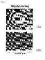
- Fig. 1 includes an exterior photo (A) showing the coil of Example 1 that was subject to the cutting-type knurling, and an exterior photo (B) showing the outside (outer surface) of this coil.
- Fig. 2 includes an SEM photo (A) showing the surface of the coil of Example 1 that was subject to the cutting-type knurling, and an SEM photo (B) showing the surface of this coil in a depth direction (cross section).
- Cutting-type knurling was performed to prepare a tantalum coil in which the surface roughness Rz is 150 ⁇ m, the number of threads is 20 TPI in a transverse direction and 13 TPI in a vertical direction, and the thread crest R is 220 ⁇ m. Even though a tantalum coil was used, the unevenness of the irregularities was large and the irregularities were distinct, and therefore the stronger adhesion of the deposited film on the surface of the tantalum coil was enabled.
- Cutting-type knurling was performed to prepare a tantalum coil in which the surface roughness Rz is 300 ⁇ m, the number of threads is 20 TPI in a transverse direction and 13 TPI in a vertical direction, and the thread crest R is 5 ⁇ m. Even though a tantalum coil was used, the unevenness of the irregularities was large and the irregularities were distinct, and therefore the stronger adhesion of the deposited film on the surface of the tantalum coil was enabled.
- the coil had conventionally needed to be replaced after the use of 200 kWh, but the tantalum coil of Example 3 could be used up to 300 kWh. It was thereby possible to yield a considerable effect.
- the thread crest R was slightly small, the deposited film started to flake at the thread crest after 300 kWh.
- a tantalum coil in which the surface roughness Rz is 250 ⁇ m, the number of threads is 18 TPI in a transverse direction and 18 TPI in a vertical direction, and the width of the flat positioned on the thread crest is 200 ⁇ m.
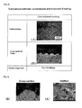
- Fig. 5 includes an SEM photo (A) showing the surface of the coil of Example 4 that was subject to the pressing-type knurling, and an SEM photo (B) showing the surface of this coil in a depth direction (cross section). Though the thread crest was flat in this case, it could also be processed to have R of 10 to 500 ⁇ m. As shown in Fig. 5 , even though a tantalum coil was used, the unevenness of the irregularities was large and the irregularities were distinct, and therefore the stronger adhesion of the deposited film on the surface of the tantalum coil was enabled.
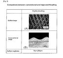
- Fig. 3 includes an exterior photo (A) showing the coil of Comparative Example 1 that was subject to the knurling, and an exterior photo (B) showing the surface of this coil.
- Fig. 4 includes an SEM photo (A) showing the surface of the coil of Comparative Example 1 that was subject to the pressing-type knurling, and an SEM photo (B) showing the surface of this coil in a depth direction (cross section).
- the unevenness of the irregularities on the surface of the tantalum coil was small, and the stronger adhesion of the deposited film on the surface of the tantalum coil could not be achieved.
- the coil needed to be replaced after the use of 200 kWh.
- Pressing-type knurling was performed to prepare a tantalum coil in which the surface roughness Rz is 20 ⁇ m, the number of threads is 80 TPI in a transverse direction and 32 TPI in a vertical direction, and the thread crest R is 550 ⁇ m.
- the unevenness of the irregularities on the surface of the tantalum coil was small, and the stronger adhesion of the deposited film on the surface of the tantalum coil could not be achieved.
- the coil needed to be replaced after the use of 100 kWh.
- the present invention is able to effectively prevent the sputtered grains accumulated on the surface of a tantalum coil from flaking so as to prevent the generation of particles and arcing that is caused by the flaking of the sputtered grains accumulated on the surface of the coil disposed between a substrate and a sputtering target, and the adhesion of the scattered flakes onto the substrate surface; and to provide a technology of improving the quality and productivity of electronic components and stably providing semiconductor elements and devices. Therefore, the present invention is applicable for a sputtering device in which a tantalum coil is used.
Landscapes
- Chemical & Material Sciences (AREA)
- Engineering & Computer Science (AREA)
- Chemical Kinetics & Catalysis (AREA)
- Materials Engineering (AREA)
- Mechanical Engineering (AREA)
- Metallurgy (AREA)
- Organic Chemistry (AREA)
- Physics & Mathematics (AREA)
- Plasma & Fusion (AREA)
- Analytical Chemistry (AREA)
- Physical Vapour Deposition (AREA)
- Electrodes Of Semiconductors (AREA)
Abstract
Description
- The present invention relates to a tantalum coil for sputtering capable of effectively inhibiting the flaking of sputtered grains accumulated on the surface of a coil that is used in a sputtering device so as to prevent the flakes of such sputtered grains from causing the generation of particles and arcing, and to the method for processing such a coil.
This tantalum coil for sputtering has a curved surface as shown in the diagrams below, and the surface of the coil covers both the inner surface and the outer surface. Accordingly, the expression "surface of the coil" refers to both the inner surface and the outer surface of the coil, and the same shall apply hereinafter. - In recent years, the sputtering method that is capable of easily controlling the film thickness and components is commonly used as one of the methods for depositing materials for use in electronic and electrical components.
The sputtering method employs a principle where: a positive electrode and a negative-electrode target are placed opposite each other; an electric field is generated by applying high voltage between the substrate and the target under an inert gas atmosphere; electrons ionized when the electric field is generated collide with the inert gas to form plasma; the positive ions in this plasma collide with the target (negative electrode) surface to discharge the constituent atoms of the target; and the extruded atoms adhere to the opposing substrate surface to form a film. - As recent sputtering technology, there is a technique of disposing a coil between the sputtering target and the substrate to increase the density of the plasma and to lead as much as possible the flying sputtered grains ballistically toward the substrate. Consequently, the sputtering rate is increased, the uniformity of the film is improved, and the quality of the film that is deposited on the substrate can be comprehensively improved.
There are cases where the material of this coil is sputtered, some are not. It depends on the bias to the coil (refer to Patent Documents 1 and 2). - Accordingly, as the material of the coil, generally used is the same material as the target material, or a material configuring a part of the materials of the sputtered film that is deposited on the substrate. Nevertheless, there is no particular limitation so as long as the coil material does not contaminate the thin film on the substrate. Moreover, as the shape of the coil, there are circular coils and spiral coils (refer to Patent Documents 1, 2, and 3), and there are cases where these coils are disposed in multiple stages.
- A problem upon forming a thin film via the foregoing sputtering method is the generation of particles. Generally speaking, the sputtered grains might also be accumulated, other than on the substrate, anywhere such as on the inner wall of the thin-film deposition system or on the internal elements therein. The sputtered grains may be accumulated on the surface other than the eroded portion, or the side surface, of the target. The particles are generated partly because the flakes from the components and the like inside the thin-film deposition system become scattered and adhere onto the substrate surface.
- Recently, while the integration of LSI semiconductor devices is increasing (16 Mb, 64 Mb and even 256 Mb), the miniaturization thereof is also improved by decreasing the line width to be 0.25 µm or less. Thus, problems of the disconnection or short-circuiting of the wiring caused by the foregoing particles now occur even more frequently.
Thus, the generation of particles is becoming an even bigger problem while the electronic device circuit continues to be further integrated and miniaturized. - However, when disposing the foregoing coil between a target and a substrate so as to increase the density of the plasma and lead as much as possible the flying sputtered grains ballistically toward the substrate, the amount of sputtered grains that will scatter and adhere, not onto the substrate, but to the inner wall of the thin-film deposition system or to the internal elements therein will decrease; but there is a problem in that the sputtered grains become accumulated on the coil itself.
In order to avoid this kind of problem, Patent Document 3 proposes that the upper end of the inner surface side of the coil is scraped off so as to reduce the thickness of the inner periphery. Here, the provided explanation is that the deposited material to become accumulated at the top of the coil slips off without remaining thereon since the shape of the upper end of the coil becomes sharper toward the top, and the coil is further cleansed since new sputtered grains will collide therewith. - Nevertheless, the portion where the deposited material will accumulate due to sputtering is not limited to the upper end of the coil. There is a possibility that the sputtered grains will also become accumulated on the surface of the coil; that is, on the outer surface and the inner surface of the coil. In the foregoing case, the flakes from the surface of the coil, where the sputtered grains have accumulated, adhere directly to the substrate surface and cause the generation of particles, but no measures are taken for this problem. Based on the demands of higher integration and further miniaturization of the circuit of electronic device, the generation of particles from the foregoing locations will also become a major problem.
- In order to resolve the foregoing problem, a proposal has been made to treat the side face of the target and the vicinity of the backing plate via blasting so as to increase the adhesion based on the anchor effect.
Nevertheless, in the foregoing case, there are the following problems; namely, contamination of the product caused by the residual blasting material, flaking of the grains that were accumulated on and adhered to the residual blasting material, and the flaking caused by the selective and non-uniform growth of the adhesive film; and therefore the foregoing blasting is not a final solution. When the coil is particularly made of a hard material like tantalum, it is difficult to even form irregularities by simply performing blasting, and it is not possible to effectively increase the adhesion.
Moreover, Patent Document 4 discloses forming, via knurling, a diamond-shaped or cross-hatch (net-like) pattern on the flange, side wall, shield, covering and the like of a target. Here, the depth is roughly 0.350 mm to 1.143 mm, but since the irregularities on the worked surface are of a simple shape, there is a possibility that a sufficient anchor effect cannot be obtained. -
- [Patent Document 1] Published Japanese Translation No. 2005-538257 of PCT Application
- [Patent Document 2] Japanese Laid-Open Patent Publication No.
2001-214264 - [Patent Document 3] Published Japanese Translation No. 2008-534777 of PCT Application
- [Patent Document 4]
W02009/099775 (PCT/US2009/031777 ) - An object of the present invention is to take measures to prevent the sputtered grains accumulated on the surface of a tantalum coil from flaking so as to prevent the generation of particles and arcing that is caused by the flaking of the sputtered grains accumulated on the coil disposed between a substrate and a sputtering target, and the adhesion of the scattered flakes onto the substrate surface; and thereby to provide a technology of improving the quality and productivity of electronic components and stably providing semiconductor elements and devices.
- Based on the above, the present invention provides:
- 1) A tantalum coil for sputtering disposed between a substrate and a sputtering target, wherein the tantalum coil has irregularities so that the surface roughness Rz of the tantalum coil is 150 µm or more and the number of threads is 15 to 30 TPI (TPI stands for "Threads per inch"; hereinafter indicated as "TPI") in a transverse direction and 10 to 30 TPI in a vertical direction;
- 2) The tantalum coil for sputtering according to 1) above, wherein the surface roughness Rz is 200 µm or more;
- 3) The tantalum coil for sputtering according to 1) above, wherein the surface roughness Rz is 250 µm or more; and
- 4) The tantalum coil for sputtering according to any one of 1) to 3) above, wherein the thread crest R is 10 to 500 µm or the thread crest is provided with a flat having a width of 10 to 500 µm.
- The present invention additionally provides:
- 5) A method for processing a tantalum coil for sputtering, wherein irregularities are formed by performing knurling to a tantalum coil disposed between a substrate and a sputtering target so that the surface roughness Rz of the tantalum coil is 150 µm or more and the number of threads is 15 to 30 TPI in a transverse direction and 10 to 30 TPI in a vertical direction;
- 6) The method for processing a tantalum coil for sputtering according to 5) above, wherein the surface roughness Rz is 200 µm or more;
- 7) The method for processing a tantalum coil for sputtering according to 5) above, wherein the surface roughness Rz is 250 µm or more; and
- 8) The method for processing a tantalum coil for sputtering according to any one of 5) to 7) above, wherein the thread crest R is 10 to 500 µm or the thread crest is provided with a flat having a width of 10 to 500 µm.
- The present invention is thereby able to effectively prevent the sputtered grains accumulated on the surface of a tantalum coil from flaking so as to prevent the generation of particles and arcing that is caused by the flaking of the sputtered grains accumulated on the surface of the coil disposed between a substrate and a sputtering target, and the adhesion of the scattered flakes onto the substrate surface; and to provide a technology of improving the quality and productivity of electronic components and stably providing semiconductor elements and devices.
-
- [
Fig. 1 ] This includes an exterior photo (A) showing the coil of Example 1 that was subject to the cutting-type knurling, and an exterior photo (B) showing the surface of this coil. - [
Fig. 2 ] This includes an SEM photo (A) showing the surface of the coil of Example 1 that was subject to the cutting-type knurling, and an SEM photo (B) showing the surface of this coil in a depth direction (cross section). - [
Fig. 3 ] This includes an exterior photo (A) showing the coil of Comparative Example 1 that was subject to the knurling, and an exterior photo (B) showing the surface of this coil. - [
Fig. 4 ] This includes an SEM photo (A) showing the surface of the coil of Comparative Example 1 that was subject to the knurling, and an SEM photo (B) showing the surface of this coil in a depth direction (cross section). - [
Fig. 5 ] This includes an SEM photo (A) showing the surface of the coil of Example 4 that was subject to the pressing-type knurling, and an SEM photo (B) showing the surface of this coil in a depth direction (cross section). - With a sputtering device in which a tantalum coil is disposed between a substrate and a sputtering target, for instance, if a tantalum target is used, the grains that are sputtered from the tantalum target will become deposited and accumulated on the wafer and also on the surface of the tantalum coil around the target. Moreover, the coil is exposed to heat and expands during sputtering.
- When the accumulation thickness on the surface of the coil increases, the film will flake due to stress increase, and such film flakes will scatter and adhere onto the substrate, and cause the generation of particles or arcing.
In order to prevent the foregoing problem, conventionally, knurling was performed to the coil so as to roughen the surface and increase the peeling resistance. Knurling is a process of forming irregularities by strongly pressing a knurling tool against the work, but there is a limit to the roughness that can be formed since tantalum is hard. - Thus, when the deposited film is accumulated to a certain degree, there is a problem in that the peeling of the film will occur in a relatively short period of time. In order to improve the quality of the thin film, it is necessary to stop the sputtering operation and replace the coil, and this caused the deterioration in the production efficiency.
Moreover, even when knurling is performed, there was a problem in that it was unclear about what extent the irregularities need to be formed on the surface so as to prevent the flaking of the sputtered grains from the surface of the coil.
Generally speaking, a thin material is used for the coil, and in certain cases a material having a thickness of roughly 5 mm is used. Thus, if strong knurling is performed, there are cases where the coil itself will deform. On the other hand, if weak knurling is performed, the roughening will be insufficient.
In the present invention, numerous tests were conducted to examine the foregoing point, and the optimal conditions were discovered by changing the method of knurling and the strength of knurling. - Consequently, it was discovered that the peeling of the deposited film can be dramatically prevented by performing knurling to a tantalum coil, which is disposed between a substrate and a sputtering target, in order to form irregularities so that the surface roughness Rz of the tantalum coil is 150 µm or more and the number of threads is 15 to 30 TPI in a transverse direction and 10 to 30 TPI in a vertical direction. There are two types of knurling processes; namely, cutting-type knurling and pressing-type knurling; and either knurling process may be applied by suitably setting the conditions.
The present invention is to provide a tantalum coil for sputtering obtained as described above. Even if one of the foregoing conditions is not met, it is not possible to prevent the flaking of the sputtered grains from the surface of the coil, and it is not possible to achieve the object of the present invention. - In addition, the surface roughness Rz is preferably 200 µm or more. It is thereby possible to roughen the irregularities and attain strong adhesion. Moreover, more preferably, the thread crest R is 10 to 500 µm or the thread crest is provided with a flat having a width of 10 to 500 µm (this size can also be referred to as the "diameter"). The tantalum coil for sputtering of the present invention provides technology which covers the foregoing aspects.
The thickness, width, and length of the coil can be arbitrarily changed based on the design of the sputtering device, and it should also be easy to understand that the coil can be arbitrarily designed to be provided in multiple stages or in a spiral shape, since these are issues related to the design of the sputtering device. - The Examples are now explained. Note that these Examples are described for facilitating the understanding of the present invention, and are not intended to limit the present invention in any way. In other words, other examples and modifications within the scope of the technical concept of the present invention are covered by the present invention.
- Cutting-type knurling was performed to prepare a tantalum coil in which the surface roughness Rz is 250 µm, the number of threads is 20 TPI (Threads per inch) in a transverse direction and 13 TPI in a vertical direction, and the thread crest R is 100 µm.
Fig. 1 includes an exterior photo (A) showing the coil of Example 1 that was subject to the cutting-type knurling, and an exterior photo (B) showing the outside (outer surface) of this coil. Moreover,Fig. 2 includes an SEM photo (A) showing the surface of the coil of Example 1 that was subject to the cutting-type knurling, and an SEM photo (B) showing the surface of this coil in a depth direction (cross section). - As shown in
Fig. 1 andFig. 2 , even though a tantalum coil was used, the unevenness of the irregularities was large and the irregularities were distinct, and therefore the stronger adhesion of the deposited film on the surface of the tantalum coil was enabled.
Moreover, when sputtering was performed using this tantalum coil, the coil had conventionally needed to be replaced after the use of 200 kWh, but the tantalum coil of Example 1 could be used up to 350 kWh. It was thereby possible to yield a considerable effect. - Cutting-type knurling was performed to prepare a tantalum coil in which the surface roughness Rz is 150 µm, the number of threads is 20 TPI in a transverse direction and 13 TPI in a vertical direction, and the thread crest R is 220 µm. Even though a tantalum coil was used, the unevenness of the irregularities was large and the irregularities were distinct, and therefore the stronger adhesion of the deposited film on the surface of the tantalum coil was enabled.
- Moreover, when sputtering was performed using this tantalum coil, the coil had conventionally needed to be replaced after the use of 200 kWh, but the tantalum coil of Example 2 could be used up to 300 kWh. It was thereby possible to yield a considerable effect. However, the use-life was shorter since the surface roughness Rz of the coil was smaller in comparison to Example 1.
- Cutting-type knurling was performed to prepare a tantalum coil in which the surface roughness Rz is 300 µm, the number of threads is 20 TPI in a transverse direction and 13 TPI in a vertical direction, and the thread crest R is 5 µm. Even though a tantalum coil was used, the unevenness of the irregularities was large and the irregularities were distinct, and therefore the stronger adhesion of the deposited film on the surface of the tantalum coil was enabled.
- Moreover, when sputtering was performed using this tantalum coil, the coil had conventionally needed to be replaced after the use of 200 kWh, but the tantalum coil of Example 3 could be used up to 300 kWh. It was thereby possible to yield a considerable effect.
However, since the thread crest R was slightly small, the deposited film started to flake at the thread crest after 300 kWh. - Pressing-type knurling was performed to prepare a tantalum coil in which the surface roughness Rz is 250 µm, the number of threads is 18 TPI in a transverse direction and 18 TPI in a vertical direction, and the width of the flat positioned on the thread crest is 200 µm.
Fig. 5 includes an SEM photo (A) showing the surface of the coil of Example 4 that was subject to the pressing-type knurling, and an SEM photo (B) showing the surface of this coil in a depth direction (cross section). Though the thread crest was flat in this case, it could also be processed to have R of 10 to 500 µm.
As shown inFig. 5 , even though a tantalum coil was used, the unevenness of the irregularities was large and the irregularities were distinct, and therefore the stronger adhesion of the deposited film on the surface of the tantalum coil was enabled. - Moreover, when sputtering was performed using this tantalum coil, the coil had conventionally needed to be replaced after the use of 200 kWh, but the tantalum coil of Example 4 could be used up to 350 kWh. It was thereby possible to yield a considerable effect.
- Pressing-type knurling was performed to prepare a tantalum coil in which the surface roughness Rz is 80 µm, the number of threads is 80 TPI in a transverse direction and 32 TPI in a vertical direction, and the thread crest R is 200 µm.
Fig. 3 includes an exterior photo (A) showing the coil of Comparative Example 1 that was subject to the knurling, and an exterior photo (B) showing the surface of this coil. Moreover,Fig. 4 includes an SEM photo (A) showing the surface of the coil of Comparative Example 1 that was subject to the pressing-type knurling, and an SEM photo (B) showing the surface of this coil in a depth direction (cross section). - As shown in
Fig. 3 andFig. 4 , the unevenness of the irregularities on the surface of the tantalum coil was small, and the stronger adhesion of the deposited film on the surface of the tantalum coil could not be achieved.
When sputtering was performed using this tantalum coil, the coil needed to be replaced after the use of 200 kWh. - Pressing-type knurling was performed to prepare a tantalum coil in which the surface roughness Rz is 20 µm, the number of threads is 80 TPI in a transverse direction and 32 TPI in a vertical direction, and the thread crest R is 550 µm. The unevenness of the irregularities on the surface of the tantalum coil was small, and the stronger adhesion of the deposited film on the surface of the tantalum coil could not be achieved. When sputtering was performed using this tantalum coil, the coil needed to be replaced after the use of 100 kWh.
- The present invention is able to effectively prevent the sputtered grains accumulated on the surface of a tantalum coil from flaking so as to prevent the generation of particles and arcing that is caused by the flaking of the sputtered grains accumulated on the surface of the coil disposed between a substrate and a sputtering target, and the adhesion of the scattered flakes onto the substrate surface; and to provide a technology of improving the quality and productivity of electronic components and stably providing semiconductor elements and devices. Therefore, the present invention is applicable for a sputtering device in which a tantalum coil is used.
Claims (8)
- A tantalum coil for sputtering disposed between a substrate and a sputtering target, wherein the tantalum coil has irregularities so that the surface roughness Rz of the tantalum coil is 150 µm or more and the number of threads is 15 to 30 TPI in a transverse direction and 10 to 30 TPI in a vertical direction.
- The tantalum coil for sputtering according to claim 1, wherein the surface roughness Rz is 200 µm or more.
- The tantalum coil for sputtering according to claim 1, wherein the surface roughness Rz is 250 µm or more.
- The tantalum coil for sputtering according to any one of claims 1 to 3, wherein the thread crest R is 10 to 500 µm or the thread crest is provided with a flat having a width of 10 to 500 µm.
- A method for processing a tantalum coil for sputtering, wherein irregularities are formed by performing knurling to a tantalum coil disposed between a substrate and a sputtering target so that the surface roughness Rz of the tantalum coil is 150 µm or more and the number of threads is 15 to 30 TPI in a transverse direction and 10 to 30 TPI in a vertical direction.
- The method for processing a tantalum coil for sputtering according to claim 5, wherein the surface roughness Rz is 200 µm or more.
- The method for processing a tantalum coil for sputtering according to claim 5, wherein the surface roughness Rz is 250 µm or more.
- The method for processing a tantalum coil for sputtering according to any one of claims 5 to 7, wherein the thread crest R is 10 to 500 µm or the thread crest is provided with a flat having a width of 10 to 500 µm.
Applications Claiming Priority (2)
| Application Number | Priority Date | Filing Date | Title |
|---|---|---|---|
| JP2010075373 | 2010-03-29 | ||
| PCT/JP2011/055916 WO2011122317A1 (en) | 2010-03-29 | 2011-03-14 | Tantalum coil for sputtering and method for processing the coil |
Publications (3)
| Publication Number | Publication Date |
|---|---|
| EP2554710A1 true EP2554710A1 (en) | 2013-02-06 |
| EP2554710A4 EP2554710A4 (en) | 2016-08-10 |
| EP2554710B1 EP2554710B1 (en) | 2017-02-22 |
Family
ID=44712038
Family Applications (1)
| Application Number | Title | Priority Date | Filing Date |
|---|---|---|---|
| EP11762557.4A Active EP2554710B1 (en) | 2010-03-29 | 2011-03-14 | Tantalum coil for sputtering and method for processing the coil |
Country Status (7)
| Country | Link |
|---|---|
| US (1) | US9371578B2 (en) |
| EP (1) | EP2554710B1 (en) |
| JP (1) | JP4763101B1 (en) |
| KR (1) | KR101385344B1 (en) |
| CN (1) | CN102791903B (en) |
| TW (1) | TWI510657B (en) |
| WO (1) | WO2011122317A1 (en) |
Families Citing this family (9)
| Publication number | Priority date | Publication date | Assignee | Title |
|---|---|---|---|---|
| CN103748258A (en) * | 2011-09-30 | 2014-04-23 | 吉坤日矿日石金属株式会社 | Regeneration method for tantalum coil for sputtering and tantlum coil obtained by regeneration method |
| CN104204282B (en) | 2012-03-21 | 2017-05-24 | 吉坤日矿日石金属株式会社 | Tantalum sputtering target, method for manufacturing same, and barrier film for semiconductor wiring formed by using target |
| US9803274B2 (en) * | 2013-11-14 | 2017-10-31 | Taiwan Semiconductor Manufacturing Co., Ltd. | Process kit of physical vapor deposition chamber and fabricating method thereof |
| US10655212B2 (en) | 2016-12-15 | 2020-05-19 | Honeywell Internatonal Inc | Sputter trap having multimodal particle size distribution |
| US20180211819A1 (en) * | 2017-01-20 | 2018-07-26 | Honeywell International Inc. | Particle trap for sputtering coil and method of making |
| US11183373B2 (en) | 2017-10-11 | 2021-11-23 | Honeywell International Inc. | Multi-patterned sputter traps and methods of making |
| CN108994525B (en) * | 2018-07-20 | 2020-08-11 | 宁波江丰电子材料股份有限公司 | Knurling process for end face of ultrahigh-purity titanium sputtering target for semiconductor |
| CN115319399A (en) * | 2022-08-26 | 2022-11-11 | 宁波江丰电子材料股份有限公司 | Method for repairing semiconductor sputtering tantalum ring |
| CN116690105B (en) * | 2023-06-30 | 2026-04-14 | 宁波江丰电子材料股份有限公司 | Treatment method for prolonging service life of high-purity target material |
Family Cites Families (21)
| Publication number | Priority date | Publication date | Assignee | Title |
|---|---|---|---|---|
| US4402359A (en) * | 1980-09-15 | 1983-09-06 | Noranda Mines Limited | Heat transfer device having an augmented wall surface |
| US5474649A (en) | 1994-03-08 | 1995-12-12 | Applied Materials, Inc. | Plasma processing apparatus employing a textured focus ring |
| WO1998031845A1 (en) | 1997-01-16 | 1998-07-23 | Bottomfield, Layne, F. | Vapor deposition components and corresponding methods |
| JP3449459B2 (en) * | 1997-06-02 | 2003-09-22 | 株式会社ジャパンエナジー | Method for manufacturing member for thin film forming apparatus and member for the apparatus |
| US6162297A (en) * | 1997-09-05 | 2000-12-19 | Applied Materials, Inc. | Embossed semiconductor fabrication parts |
| JPH11135442A (en) * | 1997-10-31 | 1999-05-21 | Canon Inc | Deposited film forming apparatus and deposited film forming method |
| US6315872B1 (en) | 1997-11-26 | 2001-11-13 | Applied Materials, Inc. | Coil for sputter deposition |
| US6376807B1 (en) * | 1999-07-09 | 2002-04-23 | Applied Materials, Inc. | Enhanced cooling IMP coil support |
| WO2002004704A2 (en) * | 2000-07-11 | 2002-01-17 | Applied Materials, Inc. | Method and apparatus for patching electrochemically deposited layers using electroless deposited materials |
| US6503380B1 (en) * | 2000-10-13 | 2003-01-07 | Honeywell International Inc. | Physical vapor target constructions |
| US6812471B2 (en) | 2002-03-13 | 2004-11-02 | Applied Materials, Inc. | Method of surface texturizing |
| US20040206804A1 (en) * | 2002-07-16 | 2004-10-21 | Jaeyeon Kim | Traps for particle entrapment in deposition chambers |
| US6955748B2 (en) | 2002-07-16 | 2005-10-18 | Honeywell International Inc. | PVD target constructions comprising projections |
| CN1806316A (en) * | 2003-06-11 | 2006-07-19 | 霍尼韦尔国际公司 | Traps for particle entrapment in deposition chambers |
| TWI342582B (en) * | 2003-07-17 | 2011-05-21 | Applied Materials Inc | Method of surface texturizing |
| US9659758B2 (en) | 2005-03-22 | 2017-05-23 | Honeywell International Inc. | Coils utilized in vapor deposition applications and methods of production |
| AU2008210504B2 (en) | 2007-01-29 | 2012-07-26 | Spinal Modulation, Inc. | Sutureless lead retention features |
| US20090194414A1 (en) * | 2008-01-31 | 2009-08-06 | Nolander Ira G | Modified sputtering target and deposition components, methods of production and uses thereof |
| CN101565819A (en) * | 2009-06-04 | 2009-10-28 | 西北稀有金属材料研究院 | Magnetic controlled sputtering ring |
| WO2012014921A1 (en) | 2010-07-30 | 2012-02-02 | Jx日鉱日石金属株式会社 | Sputtering target and/or coil and process for producing same |
| CN103748258A (en) | 2011-09-30 | 2014-04-23 | 吉坤日矿日石金属株式会社 | Regeneration method for tantalum coil for sputtering and tantlum coil obtained by regeneration method |
-
2011
- 2011-03-14 US US13/581,843 patent/US9371578B2/en active Active
- 2011-03-14 EP EP11762557.4A patent/EP2554710B1/en active Active
- 2011-03-14 WO PCT/JP2011/055916 patent/WO2011122317A1/en not_active Ceased
- 2011-03-14 JP JP2011515610A patent/JP4763101B1/en active Active
- 2011-03-14 CN CN201180013804.XA patent/CN102791903B/en active Active
- 2011-03-14 KR KR1020127020502A patent/KR101385344B1/en active Active
- 2011-03-15 TW TW100108664A patent/TWI510657B/en active
Non-Patent Citations (1)
| Title |
|---|
| See references of WO2011122317A1 * |
Also Published As
| Publication number | Publication date |
|---|---|
| US20120318668A1 (en) | 2012-12-20 |
| EP2554710A4 (en) | 2016-08-10 |
| KR20120099522A (en) | 2012-09-10 |
| EP2554710B1 (en) | 2017-02-22 |
| CN102791903B (en) | 2015-04-01 |
| JPWO2011122317A1 (en) | 2013-07-08 |
| US9371578B2 (en) | 2016-06-21 |
| TWI510657B (en) | 2015-12-01 |
| CN102791903A (en) | 2012-11-21 |
| TW201144466A (en) | 2011-12-16 |
| JP4763101B1 (en) | 2011-08-31 |
| WO2011122317A1 (en) | 2011-10-06 |
| KR101385344B1 (en) | 2014-04-14 |
Similar Documents
| Publication | Publication Date | Title |
|---|---|---|
| EP2554710B1 (en) | Tantalum coil for sputtering and method for processing the coil | |
| TWI756401B (en) | Plasma chamber target for reducing defects in workpiece during dielectric sputtering | |
| JP4623055B2 (en) | Metal film peeling prevention structure in metal film forming apparatus and semiconductor device manufacturing method using the structure | |
| EP2719793B1 (en) | Regeneration method for tantalum coil for sputtering | |
| JP2002146524A (en) | Sputtering target hardly causing generation of particle | |
| CN102782182B (en) | Sputter equipment | |
| JP6273188B2 (en) | Plasma processing method | |
| WO2016099804A1 (en) | Particle reduction in a deposition chamber using thermal expansion coefficient compatible coating | |
| TW201621072A (en) | Target assembly | |
| JP2010275574A (en) | Sputtering apparatus and semiconductor device manufacturing method | |
| WO2018148091A1 (en) | Paste method to reduce defects in dielectric sputtering | |
| TWI615492B (en) | Target assembly | |
| JP2002004038A (en) | Sputtering target with less particle generation | |
| JP4566367B2 (en) | Sputtering target with less generation of particles | |
| CN105408515A (en) | Insulating material target | |
| JP6972427B2 (en) | Film formation method | |
| JP2018117033A (en) | Semiconductor manufacturing apparatus and semiconductor manufacturing method | |
| JP2026006985A (en) | Sputtering apparatus and tungsten film forming method | |
| JP2004315948A (en) | Contamination prevention device for thin film deposition system | |
| JP6310678B2 (en) | Sputtering method | |
| JP2001026862A (en) | Sputtering target and its production |
Legal Events
| Date | Code | Title | Description |
|---|---|---|---|
| PUAI | Public reference made under article 153(3) epc to a published international application that has entered the european phase |
Free format text: ORIGINAL CODE: 0009012 |
|
| 17P | Request for examination filed |
Effective date: 20120803 |
|
| AK | Designated contracting states |
Kind code of ref document: A1 Designated state(s): AL AT BE BG CH CY CZ DE DK EE ES FI FR GB GR HR HU IE IS IT LI LT LU LV MC MK MT NL NO PL PT RO RS SE SI SK SM TR |
|
| DAX | Request for extension of the european patent (deleted) | ||
| RA4 | Supplementary search report drawn up and despatched (corrected) |
Effective date: 20160707 |
|
| RIC1 | Information provided on ipc code assigned before grant |
Ipc: H01J 37/34 20060101ALI20160701BHEP Ipc: C23C 14/44 20060101ALI20160701BHEP Ipc: C23C 14/56 20060101ALI20160701BHEP Ipc: H01L 21/285 20060101ALI20160701BHEP Ipc: C23C 14/34 20060101ALI20160701BHEP Ipc: C23C 14/00 20060101AFI20160701BHEP |
|
| GRAP | Despatch of communication of intention to grant a patent |
Free format text: ORIGINAL CODE: EPIDOSNIGR1 |
|
| INTG | Intention to grant announced |
Effective date: 20161109 |
|
| GRAS | Grant fee paid |
Free format text: ORIGINAL CODE: EPIDOSNIGR3 |
|
| GRAA | (expected) grant |
Free format text: ORIGINAL CODE: 0009210 |
|
| AK | Designated contracting states |
Kind code of ref document: B1 Designated state(s): AL AT BE BG CH CY CZ DE DK EE ES FI FR GB GR HR HU IE IS IT LI LT LU LV MC MK MT NL NO PL PT RO RS SE SI SK SM TR |
|
| REG | Reference to a national code |
Ref country code: GB Ref legal event code: FG4D |
|
| REG | Reference to a national code |
Ref country code: FR Ref legal event code: PLFP Year of fee payment: 7 |
|
| REG | Reference to a national code |
Ref country code: CH Ref legal event code: EP |
|
| REG | Reference to a national code |
Ref country code: AT Ref legal event code: REF Ref document number: 869346 Country of ref document: AT Kind code of ref document: T Effective date: 20170315 |
|
| REG | Reference to a national code |
Ref country code: IE Ref legal event code: FG4D |
|
| REG | Reference to a national code |
Ref country code: DE Ref legal event code: R096 Ref document number: 602011035224 Country of ref document: DE |
|
| REG | Reference to a national code |
Ref country code: LT Ref legal event code: MG4D |
|
| REG | Reference to a national code |
Ref country code: NL Ref legal event code: MP Effective date: 20170222 |
|
| REG | Reference to a national code |
Ref country code: AT Ref legal event code: MK05 Ref document number: 869346 Country of ref document: AT Kind code of ref document: T Effective date: 20170222 |
|
| PG25 | Lapsed in a contracting state [announced via postgrant information from national office to epo] |
Ref country code: HR Free format text: LAPSE BECAUSE OF FAILURE TO SUBMIT A TRANSLATION OF THE DESCRIPTION OR TO PAY THE FEE WITHIN THE PRESCRIBED TIME-LIMIT Effective date: 20170222 Ref country code: GR Free format text: LAPSE BECAUSE OF FAILURE TO SUBMIT A TRANSLATION OF THE DESCRIPTION OR TO PAY THE FEE WITHIN THE PRESCRIBED TIME-LIMIT Effective date: 20170523 Ref country code: LT Free format text: LAPSE BECAUSE OF FAILURE TO SUBMIT A TRANSLATION OF THE DESCRIPTION OR TO PAY THE FEE WITHIN THE PRESCRIBED TIME-LIMIT Effective date: 20170222 Ref country code: FI Free format text: LAPSE BECAUSE OF FAILURE TO SUBMIT A TRANSLATION OF THE DESCRIPTION OR TO PAY THE FEE WITHIN THE PRESCRIBED TIME-LIMIT Effective date: 20170222 Ref country code: NO Free format text: LAPSE BECAUSE OF FAILURE TO SUBMIT A TRANSLATION OF THE DESCRIPTION OR TO PAY THE FEE WITHIN THE PRESCRIBED TIME-LIMIT Effective date: 20170522 |
|
| PG25 | Lapsed in a contracting state [announced via postgrant information from national office to epo] |
Ref country code: AT Free format text: LAPSE BECAUSE OF FAILURE TO SUBMIT A TRANSLATION OF THE DESCRIPTION OR TO PAY THE FEE WITHIN THE PRESCRIBED TIME-LIMIT Effective date: 20170222 Ref country code: BG Free format text: LAPSE BECAUSE OF FAILURE TO SUBMIT A TRANSLATION OF THE DESCRIPTION OR TO PAY THE FEE WITHIN THE PRESCRIBED TIME-LIMIT Effective date: 20170522 Ref country code: LV Free format text: LAPSE BECAUSE OF FAILURE TO SUBMIT A TRANSLATION OF THE DESCRIPTION OR TO PAY THE FEE WITHIN THE PRESCRIBED TIME-LIMIT Effective date: 20170222 Ref country code: NL Free format text: LAPSE BECAUSE OF FAILURE TO SUBMIT A TRANSLATION OF THE DESCRIPTION OR TO PAY THE FEE WITHIN THE PRESCRIBED TIME-LIMIT Effective date: 20170222 Ref country code: ES Free format text: LAPSE BECAUSE OF FAILURE TO SUBMIT A TRANSLATION OF THE DESCRIPTION OR TO PAY THE FEE WITHIN THE PRESCRIBED TIME-LIMIT Effective date: 20170222 Ref country code: SE Free format text: LAPSE BECAUSE OF FAILURE TO SUBMIT A TRANSLATION OF THE DESCRIPTION OR TO PAY THE FEE WITHIN THE PRESCRIBED TIME-LIMIT Effective date: 20170222 Ref country code: PT Free format text: LAPSE BECAUSE OF FAILURE TO SUBMIT A TRANSLATION OF THE DESCRIPTION OR TO PAY THE FEE WITHIN THE PRESCRIBED TIME-LIMIT Effective date: 20170622 Ref country code: RS Free format text: LAPSE BECAUSE OF FAILURE TO SUBMIT A TRANSLATION OF THE DESCRIPTION OR TO PAY THE FEE WITHIN THE PRESCRIBED TIME-LIMIT Effective date: 20170222 |
|
| PG25 | Lapsed in a contracting state [announced via postgrant information from national office to epo] |
Ref country code: SK Free format text: LAPSE BECAUSE OF FAILURE TO SUBMIT A TRANSLATION OF THE DESCRIPTION OR TO PAY THE FEE WITHIN THE PRESCRIBED TIME-LIMIT Effective date: 20170222 Ref country code: EE Free format text: LAPSE BECAUSE OF FAILURE TO SUBMIT A TRANSLATION OF THE DESCRIPTION OR TO PAY THE FEE WITHIN THE PRESCRIBED TIME-LIMIT Effective date: 20170222 Ref country code: RO Free format text: LAPSE BECAUSE OF FAILURE TO SUBMIT A TRANSLATION OF THE DESCRIPTION OR TO PAY THE FEE WITHIN THE PRESCRIBED TIME-LIMIT Effective date: 20170222 Ref country code: IT Free format text: LAPSE BECAUSE OF FAILURE TO SUBMIT A TRANSLATION OF THE DESCRIPTION OR TO PAY THE FEE WITHIN THE PRESCRIBED TIME-LIMIT Effective date: 20170222 Ref country code: CZ Free format text: LAPSE BECAUSE OF FAILURE TO SUBMIT A TRANSLATION OF THE DESCRIPTION OR TO PAY THE FEE WITHIN THE PRESCRIBED TIME-LIMIT Effective date: 20170222 |
|
| REG | Reference to a national code |
Ref country code: CH Ref legal event code: PL |
|
| REG | Reference to a national code |
Ref country code: DE Ref legal event code: R097 Ref document number: 602011035224 Country of ref document: DE |
|
| PG25 | Lapsed in a contracting state [announced via postgrant information from national office to epo] |
Ref country code: MC Free format text: LAPSE BECAUSE OF FAILURE TO SUBMIT A TRANSLATION OF THE DESCRIPTION OR TO PAY THE FEE WITHIN THE PRESCRIBED TIME-LIMIT Effective date: 20170222 Ref country code: SM Free format text: LAPSE BECAUSE OF FAILURE TO SUBMIT A TRANSLATION OF THE DESCRIPTION OR TO PAY THE FEE WITHIN THE PRESCRIBED TIME-LIMIT Effective date: 20170222 Ref country code: PL Free format text: LAPSE BECAUSE OF FAILURE TO SUBMIT A TRANSLATION OF THE DESCRIPTION OR TO PAY THE FEE WITHIN THE PRESCRIBED TIME-LIMIT Effective date: 20170222 Ref country code: DK Free format text: LAPSE BECAUSE OF FAILURE TO SUBMIT A TRANSLATION OF THE DESCRIPTION OR TO PAY THE FEE WITHIN THE PRESCRIBED TIME-LIMIT Effective date: 20170222 |
|
| REG | Reference to a national code |
Ref country code: IE Ref legal event code: MM4A |
|
| PLBE | No opposition filed within time limit |
Free format text: ORIGINAL CODE: 0009261 |
|
| STAA | Information on the status of an ep patent application or granted ep patent |
Free format text: STATUS: NO OPPOSITION FILED WITHIN TIME LIMIT |
|
| GBPC | Gb: european patent ceased through non-payment of renewal fee |
Effective date: 20170522 |
|
| 26N | No opposition filed |
Effective date: 20171123 |
|
| PG25 | Lapsed in a contracting state [announced via postgrant information from national office to epo] |
Ref country code: LU Free format text: LAPSE BECAUSE OF NON-PAYMENT OF DUE FEES Effective date: 20170314 |
|
| REG | Reference to a national code |
Ref country code: FR Ref legal event code: PLFP Year of fee payment: 8 |
|
| PG25 | Lapsed in a contracting state [announced via postgrant information from national office to epo] |
Ref country code: LI Free format text: LAPSE BECAUSE OF NON-PAYMENT OF DUE FEES Effective date: 20170331 Ref country code: IE Free format text: LAPSE BECAUSE OF NON-PAYMENT OF DUE FEES Effective date: 20170314 Ref country code: SI Free format text: LAPSE BECAUSE OF FAILURE TO SUBMIT A TRANSLATION OF THE DESCRIPTION OR TO PAY THE FEE WITHIN THE PRESCRIBED TIME-LIMIT Effective date: 20170222 Ref country code: CH Free format text: LAPSE BECAUSE OF NON-PAYMENT OF DUE FEES Effective date: 20170331 |
|
| REG | Reference to a national code |
Ref country code: BE Ref legal event code: MM Effective date: 20170331 |
|
| PG25 | Lapsed in a contracting state [announced via postgrant information from national office to epo] |
Ref country code: GB Free format text: LAPSE BECAUSE OF NON-PAYMENT OF DUE FEES Effective date: 20170522 |
|
| PG25 | Lapsed in a contracting state [announced via postgrant information from national office to epo] |
Ref country code: BE Free format text: LAPSE BECAUSE OF NON-PAYMENT OF DUE FEES Effective date: 20170331 |
|
| PG25 | Lapsed in a contracting state [announced via postgrant information from national office to epo] |
Ref country code: MT Free format text: LAPSE BECAUSE OF NON-PAYMENT OF DUE FEES Effective date: 20170314 |
|
| PG25 | Lapsed in a contracting state [announced via postgrant information from national office to epo] |
Ref country code: HU Free format text: LAPSE BECAUSE OF FAILURE TO SUBMIT A TRANSLATION OF THE DESCRIPTION OR TO PAY THE FEE WITHIN THE PRESCRIBED TIME-LIMIT; INVALID AB INITIO Effective date: 20110314 |
|
| PG25 | Lapsed in a contracting state [announced via postgrant information from national office to epo] |
Ref country code: CY Free format text: LAPSE BECAUSE OF NON-PAYMENT OF DUE FEES Effective date: 20170222 |
|
| PG25 | Lapsed in a contracting state [announced via postgrant information from national office to epo] |
Ref country code: MK Free format text: LAPSE BECAUSE OF FAILURE TO SUBMIT A TRANSLATION OF THE DESCRIPTION OR TO PAY THE FEE WITHIN THE PRESCRIBED TIME-LIMIT Effective date: 20170222 |
|
| PG25 | Lapsed in a contracting state [announced via postgrant information from national office to epo] |
Ref country code: TR Free format text: LAPSE BECAUSE OF FAILURE TO SUBMIT A TRANSLATION OF THE DESCRIPTION OR TO PAY THE FEE WITHIN THE PRESCRIBED TIME-LIMIT Effective date: 20170222 |
|
| PG25 | Lapsed in a contracting state [announced via postgrant information from national office to epo] |
Ref country code: AL Free format text: LAPSE BECAUSE OF FAILURE TO SUBMIT A TRANSLATION OF THE DESCRIPTION OR TO PAY THE FEE WITHIN THE PRESCRIBED TIME-LIMIT Effective date: 20170222 Ref country code: IS Free format text: LAPSE BECAUSE OF FAILURE TO SUBMIT A TRANSLATION OF THE DESCRIPTION OR TO PAY THE FEE WITHIN THE PRESCRIBED TIME-LIMIT Effective date: 20170622 |
|
| P01 | Opt-out of the competence of the unified patent court (upc) registered |
Effective date: 20230517 |
|
| PGFP | Annual fee paid to national office [announced via postgrant information from national office to epo] |
Ref country code: DE Payment date: 20260128 Year of fee payment: 16 |
|
| PGFP | Annual fee paid to national office [announced via postgrant information from national office to epo] |
Ref country code: FR Payment date: 20260209 Year of fee payment: 16 |