EP2553758B1 - Waveguide system and methods - Google Patents
Waveguide system and methods Download PDFInfo
- Publication number
- EP2553758B1 EP2553758B1 EP10849136.6A EP10849136A EP2553758B1 EP 2553758 B1 EP2553758 B1 EP 2553758B1 EP 10849136 A EP10849136 A EP 10849136A EP 2553758 B1 EP2553758 B1 EP 2553758B1
- Authority
- EP
- European Patent Office
- Prior art keywords
- layers
- waveguide
- attachment
- waveguides
- waveguide surface
- Prior art date
- Legal status (The legal status is an assumption and is not a legal conclusion. Google has not performed a legal analysis and makes no representation as to the accuracy of the status listed.)
- Not-in-force
Links
- 238000000034 method Methods 0.000 title claims description 29
- 230000003287 optical effect Effects 0.000 claims description 19
- 238000004519 manufacturing process Methods 0.000 claims description 5
- 230000003746 surface roughness Effects 0.000 claims description 4
- 239000000853 adhesive Substances 0.000 claims description 3
- 230000001070 adhesive effect Effects 0.000 claims description 3
- 230000006835 compression Effects 0.000 claims description 3
- 238000007906 compression Methods 0.000 claims description 2
- 238000002347 injection Methods 0.000 claims description 2
- 239000007924 injection Substances 0.000 claims description 2
- 229920001169 thermoplastic Polymers 0.000 claims 3
- 239000004416 thermosoftening plastic Substances 0.000 claims 3
- 239000010410 layer Substances 0.000 description 86
- 239000011248 coating agent Substances 0.000 description 40
- 238000000576 coating method Methods 0.000 description 40
- 238000010586 diagram Methods 0.000 description 4
- 238000005516 engineering process Methods 0.000 description 4
- 238000004924 electrostatic deposition Methods 0.000 description 3
- 238000001771 vacuum deposition Methods 0.000 description 3
- 238000004891 communication Methods 0.000 description 2
- 230000000052 comparative effect Effects 0.000 description 2
- 238000000748 compression moulding Methods 0.000 description 2
- 238000010276 construction Methods 0.000 description 2
- 238000001125 extrusion Methods 0.000 description 2
- 238000001746 injection moulding Methods 0.000 description 2
- 239000002184 metal Substances 0.000 description 2
- 239000002356 single layer Substances 0.000 description 2
- 230000005540 biological transmission Effects 0.000 description 1
- 239000002131 composite material Substances 0.000 description 1
- 238000009434 installation Methods 0.000 description 1
- 230000035515 penetration Effects 0.000 description 1
- 230000008054 signal transmission Effects 0.000 description 1
- 239000007787 solid Substances 0.000 description 1
- 238000001228 spectrum Methods 0.000 description 1
Images





Classifications
-
- G—PHYSICS
- G02—OPTICS
- G02B—OPTICAL ELEMENTS, SYSTEMS OR APPARATUS
- G02B6/00—Light guides; Structural details of arrangements comprising light guides and other optical elements, e.g. couplings
- G02B6/24—Coupling light guides
- G02B6/42—Coupling light guides with opto-electronic elements
- G02B6/43—Arrangements comprising a plurality of opto-electronic elements and associated optical interconnections
-
- G—PHYSICS
- G02—OPTICS
- G02B—OPTICAL ELEMENTS, SYSTEMS OR APPARATUS
- G02B6/00—Light guides; Structural details of arrangements comprising light guides and other optical elements, e.g. couplings
- G02B6/10—Light guides; Structural details of arrangements comprising light guides and other optical elements, e.g. couplings of the optical waveguide type
Definitions
- optical signals i.e. signals in whole or in part within the optical portion of the electromagnetic spectrum
- optical signals increase their penetration and market share in communications applications formerly dominated by electrical signal transmission
- the ability to transmit wide bandwidth optical signals in becomes critical to meeting the demands placed upon modern optics-based communication systems.
- hollow-metal waveguides offer benefits for transmitting optical signals, their construction, application, and installation must often meet demanding requirements to ensure the integrity of the data transmitted along the waveguide.
- High speed data transmission within a computing device can be accomplished using optical signals transmitted via waveguides.
- optical data can be broadcast rather than transmitted from a source point to a destination point.
- Optical waveguides particularly hollow metal waveguides, offer an efficient, reliable conduit for broadcasting due to the ease with which beam splitters can be introduced to the collimated optical beam.
- Such waveguides are disclosed in JP2005003944 , RU2200969 , WO2009136945 , WO03065091 , and EP0357233 . With waveguide spacing as little as 250 microns, fabrication of a large number of parallel optical waveguides using conventional compression or injection molding can be difficult.
- a waveguide apparatus inlcudes a plurality of layers adapted to provide a plurality of waveguides.
- Each of the plurality of layers includes at least one alignment feature and at least one first waveguide surface.
- the apparatus further includes a first member and a second member, where the first member is at least partially attached to the second member. At least a portion of the plurality of layers are disposed between the first and second members. At least one alignment device is disposed at least partially within the at least one alignment feature.
- a method of manufacturing a waveguide according to claim 3 is also provided.
- the method includes stacking a plurality of layers to form a plurality of waveguides. Each of the plurality of layers inlcudes at least one first waveguide surface.
- the method further includes aligning the plurality of layers using at least one alignment device.
- the method also includes trapping the aligned, stacked plurality of layers between a first member and second member.
- Fig. 1 is a perspective view depicting an illustrative waveguide apparatus 100, according to one or more embodiments.
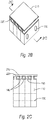
- Fig 1A is a perspective view depicting an illustrative waveguide layer 110 used in the waveguide apparatus depicted in Fig. 1 , according to one or more embodiments.
- Fig. 1B is a sectional view depicting an illustrative waveguide layer 110 used in the waveguide apparatus depicted in Fig. 1 , according to one or more embodiments.
- the waveguide apparatus 100 includes a plurality of layers 110 adapted to provide a plurality of waveguides 120. At least a portion of the layers 110 includes at least one alignment feature 130, disposed on, through, or about the layer 110. Each of the plurality of waveguides 120 includes at least one first waveguide surface 140. In one or more embodiments a second waveguide surface 150, as depicted in Figs. 1A and 1B , is disposed on all or a portion of the layers 110.
- the waveguide apparatus 100 further includes a first member 170 and a second member 180. At least a portion of the layers 110 is trapped between the first member 170 and the second member 180.
- At least one alignment device 160 passes through all or a portion of the alignment features 130 as depicted in Fig. 1 .
- the first member 170 is at least partially attached to the second member 180, for example through the use of an interconnecting a groove or channel disposed on the first member 170 with a complimentary tongue disposed on the second member 180 as depicted in Fig. 1 .
- Each of the layers forming the plurality of layers 110 can be a plastic or polymeric member, formed or otherwise produced using at least one injection molding technology, extrusion technology, compression molding technology, or the like. Such manufacturing technologies provide a rapid, cost effective, method for producing the plurality of layers 110. Since each layer 110 contains at least a portion of a single waveguide 120, issues related to alignment of multiple waveguides on a single member or surface can be minimized. Additionally, inherent flexibility is provided as any number of layers can be used to provide the plurality of layers 110, thereby providing any number of waveguides 120.
- each layer forming the plurality of layers 110 can be the same or different, i.e, the plurality of layers 110 forming the plurality of waveguides 120 can have the same or differing dimensions based upon system, user, or performance requirements.
- Each of the layers 110 can have a minimum thickness of about 100 ⁇ m or greater; about 200 ⁇ m or greater; about 300 ⁇ m or greater; about 400 ⁇ m or greater; or about 500 ⁇ m or greater.
- Each of the layers 110 can have an overall height of about 10 mm or greater; about 30 mm or greater; about 50 mm or greater; about 70 mm or greater; or about 90 mm or greater.
- Each of the layers 110 can have a length necessary to transmit or otherwise convey one or more optical signals a specified distance. For example, each of the layers 110 can have a thickness of approximately 250 ⁇ m, a length of several centimeters (cm) and a height of several millimeters (mm).
- One or more alignment features 130 are disposed in, on, or about all or a portion of the layers 110.
- the use of one or more alignment features 130 facilitates a precise alignment of the layers into a "stack" where each of the plurality of waveguides 120 lie parallel within a single plane, for example as depicted in Fig. 1 .
- the one or more alignment features 130 are disposed in, on, or about each layer 110.
- Each of the plurality of layers 110 for example, can have a protruding alignment feature 130 that complimentarily fits within a corresponding recessed alignment feature 130 on an adjacent later 110.
- the alignment feature 130 can include an aperture having any shape, size or cross section, an illustrative circular aperture is depicted in Figs. 1, 1A and 1B .
- the alignment feature 130 can accommodate the passage of one or more alignment devices 160, for example one or more shafts, through all or a portion of the layers 110.
- Each of the plurality of waveguides 120 includes at least one first waveguide surface 140. As depicted in Figs. 1, 1A and 1B , in some embodiments, each layer 110 can include two normally disposed first waveguide surfaces 140.
- a coating can be disposed on at least a portion of the first waveguide surfaces 140.
- the coating can be a reflective coating, having reflective properties at the wavelength or wavelengths of the optical signals transmitted within the plurality of waveguides 120.
- the coating can include a reflective metallic coating.
- the coating disposed on the first waveguide surfaces 140 can include a mirror-like coating, a highly-polished coating, a reflective coating, or similar.
- the coating can be a reflective coating characterized by having a surface roughness of about 70 nm Ra or less; about 50 nm Ra or less; about 30 nm Ra or less; or about 20 nm Ra or less.
- the coating can be applied at least a portion of the at least one first waveguide surface 140 using electrostatic deposition, vacuum deposition, or the like.
- Each of the layers includes a second waveguide surface 150.
- at least a portion of the second waveguide surface can be disposed distal from all or a portion of the first waveguide surface 140.
- Each of the second waveguide surfaces 150 provides at least a portion of each of the plurality of waveguides 120.
- a coating can be disposed on at least a portion of the second waveguide surface 150.
- the coating can be a reflective coating, having reflective properties at the wavelength or wavelengths of the optical signals transmitted within the plurality of waveguides 120.
- the coating can include a reflective metallic coating.
- the coating disposed on the second waveguide surface 150 can include a mirror-like coating, a highly-polished coating, a reflective coating, or similar.
- the coating can be a reflective coating characterized by having a surface roughness of about 70 nm Ra or less; about 50 nm Ra or less; about 30 nm Ra or less; or about 20 nm Ra or less.
- the coating can be applied at least a portion of the at least one second waveguide surface 150 using electrostatic deposition, vacuum deposition, or the like.
- the at least one alignment device 160 can include any number of structures, devices, fixtures, or the like suitable for aligning at least a portion of the plurality of waveguides 120.
- the at least one alignment device 160 can be used to align the plurality of waveguides 120 along a single plane as depicted in Fig. 1 .
- the at least one alignment device 160 can include a solid member, such as a pin or shaft as depicted in Fig. 1 .
- at least a portion of the at least one alignment device 160 can be attached to the first member 170, such an arrangement can permit the alignment of the plurality of layers 110 with the first member 170, thereby providing an integral, aligned, rigid, structure.
- the geometry of the alignment feature 130 disposed on each layer can closely approximate the geometry of the alignment device 160.
- the first member 170 can include any structure, device, or system adapted to support the plurality of layer 110.
- the first member 170 can include a rigid structure having any shape, size, length, or geometry.
- the first member 170 can include one or more structures to facilitate or align the connection between the first member 170 and the second member 180, for example the first member 170 can have a surface feature such as a groove into which a complimentary surface feature such as a tongue disposed on the second member 180 can be inserted, engaged, joined, or otherwise connected.
- the first member 170 can include at least one metallic member, at least one non-metallic member, at least one composite member (e.g., a laminated metallic and non-metallic member), or any combination thereof.
- the first member 170 can include one or more one injection molded members, one or more extrusion molded members, one or more compression molded members, or the like.
- the second member 180 can include any structure, device, or system adapted to support the plurality of layer 110.
- the second member 180 can include a rigid structure having any shape, size, length, or geometry.
- the second member 180 can include one or more structures to facilitate or align the connection between the first member 170 and the second member 180, for example the second member 180 can have a surface feature such as a tongue which can be inserted into a complimentary groove disposed on the first member 170.
- the second member 180 can include one or more features, for example one or more apertures as depicted in Fig. 1 , to accommodate all or a portion of the at least one alignment device 160.
- At least a portion of the at least one alignment device 160 can pass through and extend or protrude from all or a portion of the plurality of layers 110. Where at least a portion of the at least one alignment device 160 protrudes from the plurality of layers 110, one or more complimentary features, for example complimentary apertures, can be disposed in, on, or about the second member 180 to accommodate the at least one alignment device 160.
- At least a portion of the first member 170 is detachably or non-detachably attached to the second member 180.
- Such attachment can be accomplished using a variety of attachment methods such as the tongue and groove friction attachment method discussed in detail above.
- Alternative methods of attachment are also possible, for example attachment using at least one latch, attachment using at least one clamp, attachment using at least one threaded fastener, attachment using an adhesive, and attachment using a thermal weld.
- Fig. 2 is a perspective view depicting another illustrative waveguide system 200, according to one or more embodiments.
- Fig 2A is a perspective view depicting the illustrative waveguide system 200 depicted in Fig. 2 , according to one or more embodiments.
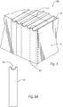
- Fig. 2B is a perspective view depicting the illustrative plurality of waveguide layers 110 from the waveguide system 200 depicted in Fig. 2 , according to one or more embodiments.
- Fig. 2C is a sectional view depicting an illustrative plurality of waveguide layers 110 from the waveguide system 200 depicted in Fig. 2 , according to one or more embodiments.
- the waveguide system 200 includes a cover member 210 disposed proximate all or a portion of the plurality of layers 110 and the plurality of waveguides 120.
- waveguide surface 220 is disposed on or about all or a portion of the cover member 210.
- the waveguide surface 220 can be disposed proximate each of the plurality of waveguides 120, thereby forming at least a portion of the interior surface of at least a portion of the plurality of waveguides 120. For example, as depicted in Figs.
- each of the plurality of waveguides 120 can include four surfaces forming a square or rectangular waveguide where two first waveguide surfaces 140 are provided by a layer 110, a single second waveguide surface 150 is provided by an adjacent layer 110, and the remaining waveguide surface 220 is provided by the cover member 210.
- a coating can be disposed on at least a portion of the cover member 210.
- the coating can be a reflective coating, having reflective properties at the wavelength or wavelengths of the optical signals transmitted within the plurality of waveguides 120.
- the coating can include a reflective metallic coating.
- the coating disposed on the cover member 210 can include a mirror-like coating, a highly-polished coating, a reflective coating, or similar.
- the coating can be a reflective coating characterized by having a surface roughness of about 70 nm Ra or less; about 50 nm Ra or less; about 30 nm Ra or less; or about 20 nm Ra or less.
- the coating can be applied at least a portion of the cover member 210 using electrostatic deposition, vacuum deposition, or the like.
- the cover member 210 can be trapped or otherwise held in place proximate the plurality of waveguides 120 by the first member 170 and the second member 180.
- the cover member 210 can be held proximate the plurality of waveguides 120 by a friction fit between the first member 170 and the second member 180.
- slots, channels, grooves or the like can be disposed in the surface of the first member 170 and the second member 180.
- Fig. 3 is a partial sectional view depicting a layer 110 having an illustrative first waveguide surface 140 and second waveguide surface 150, according to one or more embodiments.
- each of the plurality of waveguides 120 can include a plurality of square or rectangular waveguide surfaces, where the first waveguide surface 140 can have a width 310 of from about 50 ⁇ m to about 500 ⁇ m; about 75 ⁇ m to about 400 ⁇ m; about 100 ⁇ m to about 300 ⁇ m.
- each of the plurality of waveguides 120 can include a plurality of square or rectangular waveguide surfaces, where the first waveguide surface 140 can have a height 320 of from about 50 ⁇ m to about 500 ⁇ m; about 75 ⁇ m to about 400 ⁇ m; about 100 ⁇ m to about 300 ⁇ m.
- Fig. 4 is a partial sectional view depicting a comparative waveguide not forming part of the present invention.
- This waveguide system 400 can include a plurality of layers 110, each layer having three orthogonal first waveguide surfaces 140 and a single second waveguide surface 150. The disposal of three orthogonal first waveguide surfaces 140 can obviate the need for a separate cover member 210, thereby simplifying the construction of the waveguide system 400.
- each layer forming the plurality of layers 110 can vary as discussed in detail above.
- the thickness of each layer forming the plurality of layers 110 can therefore be used to provide any desired center-to-center spacing 410 of the waveguides forming the plurality of waveguides 120.
- the waveguides forming the plurality of waveguides 120 can have a center-to-center spacing 410 of from about 50 ⁇ m to about 1 mm; about 100 ⁇ m to about 700 ⁇ m; or about 150 ⁇ m to about 400 ⁇ m.
- the waveguides forming the plurality of waveguides 120 can have a center-to-center spacing 410 of about 250 ⁇ m.
- Fig. 5 is a partial perspective view depicting a further comparative waveguide not forming part of the present invention.
- Fig. 5A is an elevation view depicting an illustrative layer 110 used in the waveguide system 500 depicted in Fig.
- the first waveguide surface 140 can include a single surface disposed entirely upon a single layer 110.
- the first waveguide surface 140 can be a non-planar surface, for example a semi-circular surface.
- the use of an adjacent layer 110 to provide the second waveguide surface 150 can be superfluous where the first waveguide surface 140 provides a significant portion of the waveguide 120.
- a waveguide system can be formed using the semicircular waveguide layers 110 depicted in Figs. 5 and 5A by trapping a plurality of layers 110 between a first member 170 and a second member 180, and by disposing a cover member 210 proximate the plurality of semicircular waveguides 120.
- a coating for example a reflective coating, can be disposed on at least a portion of the waveguide surface 220 proximate each of the plurality of semicircular waveguides 120.
- Fig. 6 is a partial perspective view depicting yet another illustrative waveguide system 600, according to one or more embodiments.
- Fig. 6A is an elevation view depicting an illustrative waveguide layer 110 used in the waveguide system 600 depicted in Fig. 6 , according to one or more embodiments.
- the first waveguide surface 140 includes a single non-planar surface and the second waveguide surface 150 includes a single non-planar surface, both disposed upon a single layer 110.
- Figs. 6 is a partial perspective view depicting yet another illustrative waveguide system 600, according to one or more embodiments.
- Fig. 6A is an elevation view depicting an illustrative waveguide layer 110 used in the waveguide system 600 depicted in Fig. 6 , according to one or more embodiments.
- the first waveguide surface 140 includes a single non-planar surface and the second waveguide surface 150 includes a single non-planar surface, both disposed upon a single layer 110.
- the first waveguide surface 140 and the second waveguide surface include "mirror-image" semicircular surfaces disposed on opposing sides of each of the plurality of layers 110.
- the first waveguide surface 140 on the first layer and the second waveguide surface 150 on the adjacent layer can together provide a semicircular waveguide surface.
- a waveguide system is formed using the waveguide layers 110 depicted in Figs. 6 and 6A by trapping a plurality of such layers 110 between a first member 170 and a second member 180, and by disposing a cover member 210 proximate the plurality of semicircular waveguides 120 formed by the plurality of layers 110.
- a coating for example a reflective coating, can be disposed on at least a portion of the waveguide surface 220 proximate each of the plurality of semicircular waveguides 120.
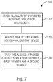
- Fig. 7 is a flow diagram depicting an illustrative waveguide method 700, according to one or more embodiments.
- the method 700 includes stacking a plurality of layers 110 to form a plurality of waveguides 120.
- the layers 110 include a first waveguide surface 140, a second waveguide surface 150, or any combination of first and second waveguide surfaces. At least a portion of the waveguide surfaces can be formed using two adjacent layers 110, where, in some embodiments, the first layer provides the first waveguide surface 140 and an adjacent layer provides the second waveguide surface 150.
- the plurality of layers 110 are aligned using at least one alignment device 160 at 720.
- the alignment is accomplished by passing, disposing, or otherwise engaging at least a portion of the at least one alignment device 160 with or through one or more alignment features 130 disposed in, on, or about the plurality of layers 110.
- the at least one alignment device can be attached to the first member 170, the second member 180, or both the first member and the second member.
- the aligned, stacked, plurality of layers 110 are at least partially trapped between the first member 170 and the second member 180 at 730.
- the aligned, stacked, plurality of layers 110 can provide a plurality of parallel waveguides 120.
- Fig. 8 is a flow diagram depicting another illustrative waveguide method 800, according to one or more embodiments.
- the first member 170 and the second member 180 trapping the stacked, aligned plurality of layers 110 at 730 are at least partially attached to each other at 810. Such attachment can occur, for example, through the use of at least one latch, at least one clamp, at least one threaded fastener, an adhesive, a thermal weld, or the like.
- the attachment of the first member to the second member can provide a sturdy, rigid, structure having a plurality of waveguides 120 disposed between the first and second members.
- a cover member 210 is disposed proximate at least a portion of the stacked, aligned plurality of layers 110 at 820.
- the cover member 210 can include one or more reflective surfaces 220 proximate at least a portion of the plurality of waveguides 120.
Landscapes
- Physics & Mathematics (AREA)
- General Physics & Mathematics (AREA)
- Optics & Photonics (AREA)
- Optical Couplings Of Light Guides (AREA)
- Optical Integrated Circuits (AREA)
Description
- The use of optical signals, i.e. signals in whole or in part within the optical portion of the electromagnetic spectrum, continues to increase due to the tremendous improvement in bandwidth and the flexibility optical signals offer over traditional electrical signals. As optical signals increase their penetration and market share in communications applications formerly dominated by electrical signal transmission, the ability to transmit wide bandwidth optical signals in becomes critical to meeting the demands placed upon modern optics-based communication systems. While hollow-metal waveguides (HMWG) offer benefits for transmitting optical signals, their construction, application, and installation must often meet demanding requirements to ensure the integrity of the data transmitted along the waveguide.
- Advantages of one or more disclosed embodiments according to claim 1 become apparent upon reading the following detailed description and upon reference to the drawings in which:
-
Fig. 1 is a perspective view depicting an illustrative waveguide system, according to one or more embodiments described herein; -
Fig 1A is a perspective view depicting an illustrative waveguide layer, according to one or more embodiments described herein; -
Fig. 1B is a sectional view depicting an illustrative waveguide layer fromFig. 1 , according to one or more embodiments described herein; -
Fig. 2 is a perspective view depicting another illustrative waveguide system, according to one or more embodiments described herein; -
Fig 2A is a perspective view depicting the illustrative waveguide layer depicted inFig. 2 , according to one or more embodiments described herein; -
Fig. 2B is a perspective view depicting an illustrative plurality of waveguide layers from the waveguide system depicted inFig. 2 , according to one or more embodiments described herein; -
Fig. 2C is a sectional view depicting an illustrative plurality of waveguide layers from the waveguide system depicted inFig. 2 , according to one or more embodiments described herein; -
Fig. 3 is a partial sectional view depicting a layer having an illustrative first waveguide surface and an illustrative second waveguide surface, according to one or more embodiments described herein; -
Fig. 4 is a partial sectional view depicting another illustrative waveguide system, not forming part of the present invention; -
Fig. 5 is a partial perspective view depicting another illustrative waveguide system, not forming part of the present invention; -
Fig. 5A is an elevation view depicting an illustrative waveguide layer used in the waveguide system depicted inFig. 5 ; -
Fig. 6 is a partial perspective view depicting yet another illustrative waveguide system, according to one or more embodiments described herein; -
Fig. 6A is an elevation view depicting an illustrative waveguide layer used in the waveguide system depicted inFig. 6 , according to one or more embodiments described herein; -
Fig. 7 is a flow diagram depicting an illustrative waveguide method, according to one or more embodiments described herein; and -
Fig. 8 is a flow diagram depicting another illustrative waveguide method, according to one or more embodiments described herein. - High speed data transmission within a computing device can be accomplished using optical signals transmitted via waveguides. To minimize cost and improve reliability, optical data can be broadcast rather than transmitted from a source point to a destination point. Optical waveguides, particularly hollow metal waveguides, offer an efficient, reliable conduit for broadcasting due to the ease with which beam splitters can be introduced to the collimated optical beam. Such waveguides are disclosed in
JP2005003944 RU2200969 WO2009136945 ,WO03065091 EP0357233 . With waveguide spacing as little as 250 microns, fabrication of a large number of parallel optical waveguides using conventional compression or injection molding can be difficult. - A waveguide apparatus according to claim 1 is provided. The waveguide apparatus inlcudes a plurality of layers adapted to provide a plurality of waveguides. Each of the plurality of layers includes at least one alignment feature and at least one first waveguide surface. The apparatus further includes a first member and a second member, where the first member is at least partially attached to the second member. At least a portion of the plurality of layers are disposed between the first and second members. At least one alignment device is disposed at least partially within the at least one alignment feature.
- A method of manufacturing a waveguide according to claim 3 is also provided. The method includes stacking a plurality of layers to form a plurality of waveguides. Each of the plurality of layers inlcudes at least one first waveguide surface. The method further includes aligning the plurality of layers using at least one alignment device. The method also includes trapping the aligned, stacked plurality of layers between a first member and second member.
- For convenience and ease of discussion,
Figs. 1, 1A and 1B will be addressed collectively.Fig. 1 is a perspective view depicting anillustrative waveguide apparatus 100, according to one or more embodiments.Fig 1A is a perspective view depicting anillustrative waveguide layer 110 used in the waveguide apparatus depicted inFig. 1 , according to one or more embodiments.Fig. 1B is a sectional view depicting anillustrative waveguide layer 110 used in the waveguide apparatus depicted inFig. 1 , according to one or more embodiments. - The
waveguide apparatus 100 includes a plurality oflayers 110 adapted to provide a plurality ofwaveguides 120. At least a portion of thelayers 110 includes at least onealignment feature 130, disposed on, through, or about thelayer 110. Each of the plurality ofwaveguides 120 includes at least onefirst waveguide surface 140. In one or more embodiments asecond waveguide surface 150, as depicted inFigs. 1A and 1B , is disposed on all or a portion of thelayers 110. Thewaveguide apparatus 100 further includes afirst member 170 and asecond member 180. At least a portion of thelayers 110 is trapped between thefirst member 170 and thesecond member 180. To align the trappedlayers 110, at least onealignment device 160 passes through all or a portion of the alignment features 130 as depicted inFig. 1 . Thefirst member 170 is at least partially attached to thesecond member 180, for example through the use of an interconnecting a groove or channel disposed on thefirst member 170 with a complimentary tongue disposed on thesecond member 180 as depicted inFig. 1 . - Each of the layers forming the plurality of
layers 110 can be a plastic or polymeric member, formed or otherwise produced using at least one injection molding technology, extrusion technology, compression molding technology, or the like. Such manufacturing technologies provide a rapid, cost effective, method for producing the plurality oflayers 110. Since eachlayer 110 contains at least a portion of asingle waveguide 120, issues related to alignment of multiple waveguides on a single member or surface can be minimized. Additionally, inherent flexibility is provided as any number of layers can be used to provide the plurality oflayers 110, thereby providing any number ofwaveguides 120. - The thickness of each layer forming the plurality of
layers 110 can be the same or different, i.e, the plurality oflayers 110 forming the plurality ofwaveguides 120 can have the same or differing dimensions based upon system, user, or performance requirements. Each of thelayers 110 can have a minimum thickness of about 100 µm or greater; about 200 µm or greater; about 300 µm or greater; about 400 µm or greater; or about 500 µm or greater. Each of thelayers 110 can have an overall height of about 10 mm or greater; about 30 mm or greater; about 50 mm or greater; about 70 mm or greater; or about 90 mm or greater. Each of thelayers 110 can have a length necessary to transmit or otherwise convey one or more optical signals a specified distance. For example, each of thelayers 110 can have a thickness of approximately 250 µm, a length of several centimeters (cm) and a height of several millimeters (mm). - One or more alignment features 130 are disposed in, on, or about all or a portion of the
layers 110. The use of one or more alignment features 130 facilitates a precise alignment of the layers into a "stack" where each of the plurality ofwaveguides 120 lie parallel within a single plane, for example as depicted inFig. 1 . The one or more alignment features 130 are disposed in, on, or about eachlayer 110. Each of the plurality oflayers 110, for example, can have a protrudingalignment feature 130 that complimentarily fits within a corresponding recessedalignment feature 130 on an adjacent later 110. In some embodiments, thealignment feature 130 can include an aperture having any shape, size or cross section, an illustrative circular aperture is depicted inFigs. 1, 1A and 1B . In some embodiments, thealignment feature 130 can accommodate the passage of one ormore alignment devices 160, for example one or more shafts, through all or a portion of thelayers 110. - Each of the plurality of
waveguides 120 includes at least onefirst waveguide surface 140. As depicted inFigs. 1, 1A and 1B , in some embodiments, eachlayer 110 can include two normally disposed first waveguide surfaces 140. - In some embodiments, a coating can be disposed on at least a portion of the first waveguide surfaces 140. In some embodiments, the coating can be a reflective coating, having reflective properties at the wavelength or wavelengths of the optical signals transmitted within the plurality of
waveguides 120. In some embodiments, the coating can include a reflective metallic coating. In some embodiment the coating disposed on the first waveguide surfaces 140 can include a mirror-like coating, a highly-polished coating, a reflective coating, or similar. In some embodiments the coating can be a reflective coating characterized by having a surface roughness of about 70 nm Ra or less; about 50 nm Ra or less; about 30 nm Ra or less; or about 20 nm Ra or less. In some embodiments, the coating can be applied at least a portion of the at least onefirst waveguide surface 140 using electrostatic deposition, vacuum deposition, or the like. - Each of the layers includes a
second waveguide surface 150. In at least some embodiments, at least a portion of the second waveguide surface can be disposed distal from all or a portion of thefirst waveguide surface 140. For example on the distal side of each of the plurality oflayers 110 opposite thefirst waveguide surface 140 as depicted inFigs. 1, 1A and 1B . Each of the second waveguide surfaces 150 provides at least a portion of each of the plurality ofwaveguides 120. - In some embodiments, a coating can be disposed on at least a portion of the
second waveguide surface 150. In some embodiments, the coating can be a reflective coating, having reflective properties at the wavelength or wavelengths of the optical signals transmitted within the plurality ofwaveguides 120. In some embodiments, the coating can include a reflective metallic coating. In some embodiment the coating disposed on thesecond waveguide surface 150 can include a mirror-like coating, a highly-polished coating, a reflective coating, or similar. In some embodiments the coating can be a reflective coating characterized by having a surface roughness of about 70 nm Ra or less; about 50 nm Ra or less; about 30 nm Ra or less; or about 20 nm Ra or less. In some embodiments, the coating can be applied at least a portion of the at least onesecond waveguide surface 150 using electrostatic deposition, vacuum deposition, or the like. - The at least one
alignment device 160 can include any number of structures, devices, fixtures, or the like suitable for aligning at least a portion of the plurality ofwaveguides 120. For example, the at least onealignment device 160 can be used to align the plurality ofwaveguides 120 along a single plane as depicted inFig. 1 . In some embodiments, the at least onealignment device 160 can include a solid member, such as a pin or shaft as depicted inFig. 1 . In some embodiments, at least a portion of the at least onealignment device 160 can be attached to thefirst member 170, such an arrangement can permit the alignment of the plurality oflayers 110 with thefirst member 170, thereby providing an integral, aligned, rigid, structure. To maintain the alignment of the plurality oflayers 110, the geometry of thealignment feature 130 disposed on each layer can closely approximate the geometry of thealignment device 160. - The
first member 170 can include any structure, device, or system adapted to support the plurality oflayer 110. Thefirst member 170 can include a rigid structure having any shape, size, length, or geometry. In at least some embodiments, thefirst member 170 can include one or more structures to facilitate or align the connection between thefirst member 170 and thesecond member 180, for example thefirst member 170 can have a surface feature such as a groove into which a complimentary surface feature such as a tongue disposed on thesecond member 180 can be inserted, engaged, joined, or otherwise connected. - In some embodiments, the
first member 170 can include at least one metallic member, at least one non-metallic member, at least one composite member (e.g., a laminated metallic and non-metallic member), or any combination thereof. In at least some embodiments, thefirst member 170 can include one or more one injection molded members, one or more extrusion molded members, one or more compression molded members, or the like. - Similar to the
first member 170, thesecond member 180 can include any structure, device, or system adapted to support the plurality oflayer 110. Thesecond member 180 can include a rigid structure having any shape, size, length, or geometry. In at least some embodiments, thesecond member 180 can include one or more structures to facilitate or align the connection between thefirst member 170 and thesecond member 180, for example thesecond member 180 can have a surface feature such as a tongue which can be inserted into a complimentary groove disposed on thefirst member 170. In some embodiments, thesecond member 180 can include one or more features, for example one or more apertures as depicted inFig. 1 , to accommodate all or a portion of the at least onealignment device 160. - In some embodiments, for example as depicted in
Fig. 1 , at least a portion of the at least onealignment device 160 can pass through and extend or protrude from all or a portion of the plurality oflayers 110. Where at least a portion of the at least onealignment device 160 protrudes from the plurality oflayers 110, one or more complimentary features, for example complimentary apertures, can be disposed in, on, or about thesecond member 180 to accommodate the at least onealignment device 160. - At least a portion of the
first member 170 is detachably or non-detachably attached to thesecond member 180. Such attachment can be accomplished using a variety of attachment methods such as the tongue and groove friction attachment method discussed in detail above. Alternative methods of attachment are also possible, for example attachment using at least one latch, attachment using at least one clamp, attachment using at least one threaded fastener, attachment using an adhesive, and attachment using a thermal weld. - For convenience and ease of discussion,
Figs. 2, 2A ,2B, and 2C will be addressed collectively.Fig. 2 is a perspective view depicting anotherillustrative waveguide system 200, according to one or more embodiments.Fig 2A is a perspective view depicting theillustrative waveguide system 200 depicted inFig. 2 , according to one or more embodiments.Fig. 2B is a perspective view depicting the illustrative plurality ofwaveguide layers 110 from thewaveguide system 200 depicted inFig. 2 , according to one or more embodiments.Fig. 2C is a sectional view depicting an illustrative plurality ofwaveguide layers 110 from thewaveguide system 200 depicted inFig. 2 , according to one or more embodiments. - The
waveguide system 200 includes acover member 210 disposed proximate all or a portion of the plurality oflayers 110 and the plurality ofwaveguides 120.waveguide surface 220 is disposed on or about all or a portion of thecover member 210. In some embodiments, thewaveguide surface 220 can be disposed proximate each of the plurality ofwaveguides 120, thereby forming at least a portion of the interior surface of at least a portion of the plurality ofwaveguides 120. For example, as depicted inFigs. 2B and 2C , each of the plurality ofwaveguides 120 can include four surfaces forming a square or rectangular waveguide where two first waveguide surfaces 140 are provided by alayer 110, a singlesecond waveguide surface 150 is provided by anadjacent layer 110, and the remainingwaveguide surface 220 is provided by thecover member 210. - In some embodiments, a coating can be disposed on at least a portion of the
cover member 210. In some embodiments, the coating can be a reflective coating, having reflective properties at the wavelength or wavelengths of the optical signals transmitted within the plurality ofwaveguides 120. In some embodiments, the coating can include a reflective metallic coating. In some embodiment the coating disposed on thecover member 210 can include a mirror-like coating, a highly-polished coating, a reflective coating, or similar. In some embodiments the coating can be a reflective coating characterized by having a surface roughness of about 70 nm Ra or less; about 50 nm Ra or less; about 30 nm Ra or less; or about 20 nm Ra or less. In some embodiments, the coating can be applied at least a portion of thecover member 210 using electrostatic deposition, vacuum deposition, or the like. - In some embodiments, the
cover member 210 can be trapped or otherwise held in place proximate the plurality ofwaveguides 120 by thefirst member 170 and thesecond member 180. For example, in some embodiments, thecover member 210 can be held proximate the plurality ofwaveguides 120 by a friction fit between thefirst member 170 and thesecond member 180. In other embodiments, slots, channels, grooves or the like can be disposed in the surface of thefirst member 170 and thesecond member 180. -
Fig. 3 is a partial sectional view depicting alayer 110 having an illustrativefirst waveguide surface 140 andsecond waveguide surface 150, according to one or more embodiments. In some embodiments, each of the plurality ofwaveguides 120 can include a plurality of square or rectangular waveguide surfaces, where thefirst waveguide surface 140 can have awidth 310 of from about 50 µm to about 500 µm; about 75 µm to about 400 µm; about 100 µm to about 300 µm. In some embodiments, each of the plurality ofwaveguides 120 can include a plurality of square or rectangular waveguide surfaces, where thefirst waveguide surface 140 can have aheight 320 of from about 50 µm to about 500 µm; about 75 µm to about 400 µm; about 100 µm to about 300 µm. -
Fig. 4 is a partial sectional view depicting a comparative waveguide not forming part of the present invention. Thiswaveguide system 400 can include a plurality oflayers 110, each layer having three orthogonal first waveguide surfaces 140 and a singlesecond waveguide surface 150. The disposal of three orthogonal first waveguide surfaces 140 can obviate the need for aseparate cover member 210, thereby simplifying the construction of thewaveguide system 400. - The thickness of each layer forming the plurality of
layers 110 can vary as discussed in detail above. The thickness of each layer forming the plurality oflayers 110 can therefore be used to provide any desired center-to-center spacing 410 of the waveguides forming the plurality ofwaveguides 120. The waveguides forming the plurality ofwaveguides 120 can have a center-to-center spacing 410 of from about 50 µm to about 1 mm; about 100 µm to about 700 µm; or about 150 µm to about 400 µm. In at least some embodiments, the waveguides forming the plurality ofwaveguides 120 can have a center-to-center spacing 410 of about 250 µm. - For convenience and ease of discussion,
Figs. 5 and 5A will be addressed collectively.Fig. 5 is a partial perspective view depicting a further comparative waveguide not forming part of the present invention.Fig. 5A is an elevation view depicting anillustrative layer 110 used in thewaveguide system 500 depicted in Fig. As depicted inFigs. 5 and 5A , thefirst waveguide surface 140 can include a single surface disposed entirely upon asingle layer 110. As depicted inFigs. 5 and 5A , thefirst waveguide surface 140 can be a non-planar surface, for example a semi-circular surface. The use of anadjacent layer 110 to provide thesecond waveguide surface 150 can be superfluous where thefirst waveguide surface 140 provides a significant portion of thewaveguide 120. - A waveguide system can be formed using the semicircular waveguide layers 110 depicted in
Figs. 5 and 5A by trapping a plurality oflayers 110 between afirst member 170 and asecond member 180, and by disposing acover member 210 proximate the plurality ofsemicircular waveguides 120. As described previously, a coating, for example a reflective coating, can be disposed on at least a portion of thewaveguide surface 220 proximate each of the plurality ofsemicircular waveguides 120. - For convenience and ease of discussion,
Figs. 6 and 6A will be addressed collectively.Fig. 6 is a partial perspective view depicting yet another illustrative waveguide system 600, according to one or more embodiments.Fig. 6A is an elevation view depicting anillustrative waveguide layer 110 used in the waveguide system 600 depicted inFig. 6 , according to one or more embodiments. As depicted inFigs. 6 and 6A in at least some embodiments, thefirst waveguide surface 140 includes a single non-planar surface and thesecond waveguide surface 150 includes a single non-planar surface, both disposed upon asingle layer 110. As depicted inFigs. 6 and 6A , in at least some embodiments, thefirst waveguide surface 140 and the second waveguide surface include "mirror-image" semicircular surfaces disposed on opposing sides of each of the plurality oflayers 110. When disposed proximate another layer, thefirst waveguide surface 140 on the first layer and thesecond waveguide surface 150 on the adjacent layer can together provide a semicircular waveguide surface. - A waveguide system is formed using the waveguide layers 110 depicted in
Figs. 6 and 6A by trapping a plurality ofsuch layers 110 between afirst member 170 and asecond member 180, and by disposing acover member 210 proximate the plurality ofsemicircular waveguides 120 formed by the plurality oflayers 110. In some embodiments, as described previously, a coating, for example a reflective coating, can be disposed on at least a portion of thewaveguide surface 220 proximate each of the plurality ofsemicircular waveguides 120. -
Fig. 7 is a flow diagram depicting anillustrative waveguide method 700, according to one or more embodiments. Themethod 700 includes stacking a plurality oflayers 110 to form a plurality ofwaveguides 120. Thelayers 110 include afirst waveguide surface 140, asecond waveguide surface 150, or any combination of first and second waveguide surfaces. At least a portion of the waveguide surfaces can be formed using twoadjacent layers 110, where, in some embodiments, the first layer provides thefirst waveguide surface 140 and an adjacent layer provides thesecond waveguide surface 150. - The plurality of
layers 110 are aligned using at least onealignment device 160 at 720. The alignment is accomplished by passing, disposing, or otherwise engaging at least a portion of the at least onealignment device 160 with or through one or more alignment features 130 disposed in, on, or about the plurality oflayers 110. In some embodiments, the at least one alignment device can be attached to thefirst member 170, thesecond member 180, or both the first member and the second member. - The aligned, stacked, plurality of
layers 110 are at least partially trapped between thefirst member 170 and thesecond member 180 at 730. In at least some embodiments, the aligned, stacked, plurality oflayers 110 can provide a plurality ofparallel waveguides 120. -
Fig. 8 is a flow diagram depicting anotherillustrative waveguide method 800, according to one or more embodiments. Thefirst member 170 and thesecond member 180 trapping the stacked, aligned plurality oflayers 110 at 730 are at least partially attached to each other at 810. Such attachment can occur, for example, through the use of at least one latch, at least one clamp, at least one threaded fastener, an adhesive, a thermal weld, or the like. The attachment of the first member to the second member can provide a sturdy, rigid, structure having a plurality ofwaveguides 120 disposed between the first and second members. - A
cover member 210 is disposed proximate at least a portion of the stacked, aligned plurality oflayers 110 at 820. In some embodiments, thecover member 210 can include one or morereflective surfaces 220 proximate at least a portion of the plurality ofwaveguides 120.
Claims (11)
- An optical waveguide apparatus, comprising:a plurality of layers (110) adapted to provide a plurality of hollow optical waveguides (120);wherein each of the plurality of layers comprises at least one first waveguide surface (140), and the plurality of layers are arranged to form a stacked plurality of layers; andwherein each waveguide (120) is formed from a waveguide surface provided by a layer and at least one of a waveguide surface provided by an adjacent layer and a waveguide surface provided by a cover member (210); the optical waveguide apparatus being characterised in that each of the plurality of layers comprises at least one alignment feature (130), and in that it comprises a first member (170) and a second member (180);wherein at least a portion of the first member is attached to at least a portion of the second member; andwherein at least a portion of the stacked plurality of layers is disposed between the first and second members; andat least one alignment device (160) disposed at least partially within the at least one alignment feature to align the layers.
- The apparatus of claim 1, wherein at least a portion of the first member (170) and the second member (180) are attached using an attachment method selected from the group of attachment methods consisting of: attachment using at least one latch, attachment using at least one clamp, attachment using at least one threaded fastener, attachment using an adhesive, and attachment using a thermal weld.
- A method of manufacturing a waveguide apparatus comprising:stacking a plurality of layers (110) to form a plurality of hollow optical waveguides (120);wherein each of the plurality of layers comprises at least one first waveguide surface (140);wherein forming the waveguides (120) comprises forming the waveguides from a waveguide surface provided by a layer and at least one of a waveguide surface provided by an adjacent layer and a waveguide surface provided by a cover member the method being characterised in that each layer comprises at least one alignment feature, and in that it comprises the further steps of providing a first member (170) and a second member (180), attaching at least a portion of the first member to at least a portion of the second member, disposing at least a portion of the stacked plurality of layers between the first and the second member, and aligning the stacked plurality of layers with at least one alignment device (160) disposed at least partially within the at least one alignment feature (180).
- The method of claim 3 further comprising: attaching a cover member (210) comprising at least one waveguide surface (220) to at least a portion of the plurality of layers.
- The method of claim 3 wherein each of the plurality of layers (110) comprises a thermoplastic member; and
wherein the thermoplastic member is selected from the group of thermoplastic members consisting of: an injection molded member and an extruded member and a compression molded member. - The method of claim 3, wherein each of the alignment devices (160) comprises at least one surface feature attached to the first member (170).
- The method of claim 6 wherein each of the alignment devices (160) comprises at least one projecting surface feature attached to the first member (170);
wherein each of the layers further comprises at least one aperture (130) adapted to accommodate the passage of at least a portion of at least one alignment device; and
wherein the second member (180) further comprises at least one aperture adapted to accommodate the passage of at least a portion of at least one alignment device. - The method of claim 3, wherein attaching at least a portion of the first member (170) to the second member (180) comprises non-detachably attaching at least a portion of the first member to at least a portion of the second member; and
wherein non-detachably attaching at least a portion of the first member to at least a portion of the second member comprises an attachment method selected from the group of attachment methods consisting of: an adhesive- based attachment method, and a thermal weld based attachment method. - The method of claim 3, wherein attaching at least a portion of the first member (170) to the second member (180) comprises detachably attaching at least a portion of the first member to at least a portion of the second member; and wherein detachably attaching at least a portion of the first member to at least a portion of the second member comprises an attachment method selected from the group of attachment methods consisting of: at least one clamp, at least one latch, and at least one threaded fastener.
- The method of claim 3 further comprising fabricating the first waveguide surface to a finish, characterized by a surface roughness in the range of 30nm Ra or less.
- The method of claim 3, wherein the plurality of waveguides (120) comprise a width (310) of from about 100 µm to about 300 µm and a height (320) of from about 100 µm to about 300 µm and/or wherein the plurality of waveguides (120) comprise a center-to-center spacing (430) of from about 150 µm to about 400 µm.
Applications Claiming Priority (1)
| Application Number | Priority Date | Filing Date | Title |
|---|---|---|---|
| PCT/US2010/029411 WO2011123111A1 (en) | 2010-03-31 | 2010-03-31 | Waveguide system and methods |
Publications (3)
| Publication Number | Publication Date |
|---|---|
| EP2553758A1 EP2553758A1 (en) | 2013-02-06 |
| EP2553758A4 EP2553758A4 (en) | 2014-05-28 |
| EP2553758B1 true EP2553758B1 (en) | 2018-08-08 |
Family
ID=44712535
Family Applications (1)
| Application Number | Title | Priority Date | Filing Date |
|---|---|---|---|
| EP10849136.6A Not-in-force EP2553758B1 (en) | 2010-03-31 | 2010-03-31 | Waveguide system and methods |
Country Status (4)
| Country | Link |
|---|---|
| US (1) | US9014526B2 (en) |
| EP (1) | EP2553758B1 (en) |
| CN (1) | CN102812591B (en) |
| WO (1) | WO2011123111A1 (en) |
Citations (6)
| Publication number | Priority date | Publication date | Assignee | Title |
|---|---|---|---|---|
| EP0490698A1 (en) * | 1990-12-13 | 1992-06-17 | The Furukawa Electric Co., Ltd. | Method of stacking ferrules of a stacked-type optical connector and a stacked-type optical connector |
| US5600747A (en) * | 1994-08-12 | 1997-02-04 | The Furukawa Electric Co., Ltd. | Method of collectively connecting multiple optical connectors and aligning and positioning jig for multiple optical connectors used in the method |
| RU2200969C2 (en) * | 2001-03-05 | 2003-03-20 | Институт химической кинетики и горения СО РАН | Multichannel optical waveguide (versions) |
| WO2003065091A2 (en) * | 2002-01-29 | 2003-08-07 | Qinetiq Limited | Optical circuit including hollow core optical waveguides |
| JP2005003944A (en) * | 2003-06-12 | 2005-01-06 | Ngk Spark Plug Co Ltd | Optical waveguide structure and manufacturing method thereof |
| WO2009136945A1 (en) * | 2008-05-09 | 2009-11-12 | Hewlett-Packard Development Company, L.P. | Methods for fabrication of large core hollow waveguides |
Family Cites Families (18)
| Publication number | Priority date | Publication date | Assignee | Title |
|---|---|---|---|---|
| EP0357233A3 (en) | 1988-08-31 | 1990-08-29 | Marconi Electronic Devices Limited | Waveguide apparatus |
| JPH10224120A (en) | 1997-02-06 | 1998-08-21 | Murata Mfg Co Ltd | Dielectric line |
| JPH11308021A (en) | 1998-04-23 | 1999-11-05 | Nec Corp | Connection structure for high frequency package |
| US6381380B1 (en) | 1998-06-24 | 2002-04-30 | The Trustees Of Princeton University | Twin waveguide based design for photonic integrated circuits |
| US6756866B1 (en) | 2000-09-29 | 2004-06-29 | Innovative Technology Licensing, Llc | Phase shifting waveguide with alterable impedance walls and module utilizing the waveguides for beam phase shifting and steering |
| JP2002358789A (en) | 2001-05-31 | 2002-12-13 | Mitsubishi Chemicals Corp | Optical memory device and reproducing method thereof |
| WO2003003066A2 (en) | 2001-06-29 | 2003-01-09 | Xanoptix, Inc. | Multi-piece fiber optic component and manufacturing technique |
| US20030174998A1 (en) * | 2002-03-15 | 2003-09-18 | George Shevchuk | Assembly for stacking optical fibers in an aligned two dimensional array |
| JP3862633B2 (en) | 2002-08-14 | 2006-12-27 | 東京エレクトロン株式会社 | Method for manufacturing non-radiative dielectric line |
| CN1222792C (en) | 2003-10-14 | 2005-10-12 | 武汉光迅科技有限责任公司 | 3-D optical-wave-guide structure and manufacturing method |
| CN101385190A (en) | 2003-12-24 | 2009-03-11 | 莫莱克斯公司 | Multichannel wave-guide construction |
| JP2006145623A (en) | 2004-11-16 | 2006-06-08 | Bridgestone Corp | Multi-step index type plastic optical waveguide |
| WO2008105404A1 (en) | 2007-02-27 | 2008-09-04 | Keio University | Polymer parallel optical waveguide and its manufacturing method |
| US7477809B1 (en) | 2007-07-31 | 2009-01-13 | Hewlett-Packard Development Company, L.P. | Photonic guiding device |
| US8072065B2 (en) | 2008-02-14 | 2011-12-06 | Viasat, Inc. | System and method for integrated waveguide packaging |
| JP5281075B2 (en) * | 2008-03-27 | 2013-09-04 | 京セラ株式会社 | Composite optical transmission board and optical module |
| KR101434237B1 (en) | 2008-03-28 | 2014-08-27 | 휴렛-팩커드 디벨롭먼트 컴퍼니, 엘.피. | Flexible optical interconnect |
| JP5526659B2 (en) | 2008-09-25 | 2014-06-18 | ソニー株式会社 | Millimeter-wave dielectric transmission device |
-
2010
- 2010-03-31 EP EP10849136.6A patent/EP2553758B1/en not_active Not-in-force
- 2010-03-31 WO PCT/US2010/029411 patent/WO2011123111A1/en not_active Ceased
- 2010-03-31 US US13/387,036 patent/US9014526B2/en active Active
- 2010-03-31 CN CN201080065887.2A patent/CN102812591B/en not_active Expired - Fee Related
Patent Citations (6)
| Publication number | Priority date | Publication date | Assignee | Title |
|---|---|---|---|---|
| EP0490698A1 (en) * | 1990-12-13 | 1992-06-17 | The Furukawa Electric Co., Ltd. | Method of stacking ferrules of a stacked-type optical connector and a stacked-type optical connector |
| US5600747A (en) * | 1994-08-12 | 1997-02-04 | The Furukawa Electric Co., Ltd. | Method of collectively connecting multiple optical connectors and aligning and positioning jig for multiple optical connectors used in the method |
| RU2200969C2 (en) * | 2001-03-05 | 2003-03-20 | Институт химической кинетики и горения СО РАН | Multichannel optical waveguide (versions) |
| WO2003065091A2 (en) * | 2002-01-29 | 2003-08-07 | Qinetiq Limited | Optical circuit including hollow core optical waveguides |
| JP2005003944A (en) * | 2003-06-12 | 2005-01-06 | Ngk Spark Plug Co Ltd | Optical waveguide structure and manufacturing method thereof |
| WO2009136945A1 (en) * | 2008-05-09 | 2009-11-12 | Hewlett-Packard Development Company, L.P. | Methods for fabrication of large core hollow waveguides |
Also Published As
| Publication number | Publication date |
|---|---|
| WO2011123111A1 (en) | 2011-10-06 |
| US20120134638A1 (en) | 2012-05-31 |
| US9014526B2 (en) | 2015-04-21 |
| EP2553758A4 (en) | 2014-05-28 |
| CN102812591B (en) | 2015-11-25 |
| EP2553758A1 (en) | 2013-02-06 |
| CN102812591A (en) | 2012-12-05 |
Similar Documents
| Publication | Publication Date | Title |
|---|---|---|
| US7665911B2 (en) | Optical waveguide holding device and optical transceiver | |
| US6085000A (en) | Wavelength division multiplexing optical device and manufacturing method therefor | |
| US10371904B2 (en) | Optical coupling structures | |
| EP2261709B1 (en) | Optical coupling device with optical waveguide coupled to optical device | |
| US20140010499A1 (en) | Optical connector ferrule | |
| US10416393B2 (en) | Connector for waveguide and alignment method | |
| US12392959B2 (en) | Optical waveguide connecting device | |
| US5574817A (en) | Fiber optic ribbon cable assembly and method of manufacturing same | |
| CN104115047B (en) | Tabula rasa | |
| EP2843460A1 (en) | Optical beam couplers and splitters | |
| US5020871A (en) | Optical fiber wiring apparatus | |
| WO2007080932A1 (en) | Optical cable module and apparatus employing it | |
| US20040114902A1 (en) | Apparatus and method for creating a fiber optic circuit | |
| US9014526B2 (en) | Waveguide system and methods | |
| KR20210089342A (en) | Flexible flat cable and method for manufacturing the same | |
| US8737785B2 (en) | Optical beam couplers and splitters | |
| US8472761B2 (en) | Waveguide systems and methods | |
| JP3844991B2 (en) | Optical wiring connection structure | |
| JP2018013640A (en) | Optical wiring parts, optical connector connection structure, and electronic equipment | |
| JP3357979B2 (en) | Optical wavelength multiplexer / demultiplexer | |
| CN105242354A (en) | Rectangular optic fiber array device and manufacturing method | |
| KR101034213B1 (en) | Optical printed circuit board and its manufacturing method | |
| KR100403740B1 (en) | Optical fiber array equipment structure | |
| EP4231075A1 (en) | Fanout tube for a furcation of a fiber optic cable and related method | |
| US7277613B2 (en) | Optical multiplexer/demultiplexer, optical communication system and method of manufacturing the optical multiplexer/demultiplexer |
Legal Events
| Date | Code | Title | Description |
|---|---|---|---|
| PUAI | Public reference made under article 153(3) epc to a published international application that has entered the european phase |
Free format text: ORIGINAL CODE: 0009012 |
|
| 17P | Request for examination filed |
Effective date: 20120124 |
|
| AK | Designated contracting states |
Kind code of ref document: A1 Designated state(s): AT BE BG CH CY CZ DE DK EE ES FI FR GB GR HR HU IE IS IT LI LT LU LV MC MK MT NL NO PL PT RO SE SI SK SM TR |
|
| DAX | Request for extension of the european patent (deleted) | ||
| A4 | Supplementary search report drawn up and despatched |
Effective date: 20140429 |
|
| RIC1 | Information provided on ipc code assigned before grant |
Ipc: H01P 5/107 20060101ALI20140423BHEP Ipc: H01P 5/103 20060101ALI20140423BHEP Ipc: H01P 11/00 20060101ALI20140423BHEP Ipc: H01P 9/00 20060101AFI20140423BHEP |
|
| RIN1 | Information on inventor provided before grant (corrected) |
Inventor name: ROESNER, ARLEN Inventor name: TAN, MICHAEL Inventor name: ROSENBERG, PAUL Inventor name: MATHAI, SAGI |
|
| RAP1 | Party data changed (applicant data changed or rights of an application transferred) |
Owner name: HEWLETT PACKARD ENTERPRISE DEVELOPMENT L.P. |
|
| 17Q | First examination report despatched |
Effective date: 20160801 |
|
| STAA | Information on the status of an ep patent application or granted ep patent |
Free format text: STATUS: EXAMINATION IS IN PROGRESS |
|
| REG | Reference to a national code |
Ref country code: DE Ref legal event code: R079 Ref document number: 602010052659 Country of ref document: DE Free format text: PREVIOUS MAIN CLASS: H01P0009000000 Ipc: G02B0006100000 |
|
| GRAP | Despatch of communication of intention to grant a patent |
Free format text: ORIGINAL CODE: EPIDOSNIGR1 |
|
| STAA | Information on the status of an ep patent application or granted ep patent |
Free format text: STATUS: GRANT OF PATENT IS INTENDED |
|
| RIC1 | Information provided on ipc code assigned before grant |
Ipc: G02B 6/10 20060101AFI20180326BHEP Ipc: G02B 6/43 20060101ALI20180326BHEP |
|
| INTG | Intention to grant announced |
Effective date: 20180420 |
|
| GRAS | Grant fee paid |
Free format text: ORIGINAL CODE: EPIDOSNIGR3 |
|
| GRAA | (expected) grant |
Free format text: ORIGINAL CODE: 0009210 |
|
| STAA | Information on the status of an ep patent application or granted ep patent |
Free format text: STATUS: THE PATENT HAS BEEN GRANTED |
|
| AK | Designated contracting states |
Kind code of ref document: B1 Designated state(s): AT BE BG CH CY CZ DE DK EE ES FI FR GB GR HR HU IE IS IT LI LT LU LV MC MK MT NL NO PL PT RO SE SI SK SM TR |
|
| REG | Reference to a national code |
Ref country code: GB Ref legal event code: FG4D |
|
| REG | Reference to a national code |
Ref country code: CH Ref legal event code: EP Ref country code: AT Ref legal event code: REF Ref document number: 1027658 Country of ref document: AT Kind code of ref document: T Effective date: 20180815 |
|
| REG | Reference to a national code |
Ref country code: IE Ref legal event code: FG4D |
|
| REG | Reference to a national code |
Ref country code: DE Ref legal event code: R096 Ref document number: 602010052659 Country of ref document: DE |
|
| REG | Reference to a national code |
Ref country code: NL Ref legal event code: MP Effective date: 20180808 |
|
| REG | Reference to a national code |
Ref country code: LT Ref legal event code: MG4D |
|
| REG | Reference to a national code |
Ref country code: AT Ref legal event code: MK05 Ref document number: 1027658 Country of ref document: AT Kind code of ref document: T Effective date: 20180808 |
|
| PG25 | Lapsed in a contracting state [announced via postgrant information from national office to epo] |
Ref country code: BG Free format text: LAPSE BECAUSE OF FAILURE TO SUBMIT A TRANSLATION OF THE DESCRIPTION OR TO PAY THE FEE WITHIN THE PRESCRIBED TIME-LIMIT Effective date: 20181108 Ref country code: SE Free format text: LAPSE BECAUSE OF FAILURE TO SUBMIT A TRANSLATION OF THE DESCRIPTION OR TO PAY THE FEE WITHIN THE PRESCRIBED TIME-LIMIT Effective date: 20180808 Ref country code: AT Free format text: LAPSE BECAUSE OF FAILURE TO SUBMIT A TRANSLATION OF THE DESCRIPTION OR TO PAY THE FEE WITHIN THE PRESCRIBED TIME-LIMIT Effective date: 20180808 Ref country code: GR Free format text: LAPSE BECAUSE OF FAILURE TO SUBMIT A TRANSLATION OF THE DESCRIPTION OR TO PAY THE FEE WITHIN THE PRESCRIBED TIME-LIMIT Effective date: 20181109 Ref country code: NL Free format text: LAPSE BECAUSE OF FAILURE TO SUBMIT A TRANSLATION OF THE DESCRIPTION OR TO PAY THE FEE WITHIN THE PRESCRIBED TIME-LIMIT Effective date: 20180808 Ref country code: LT Free format text: LAPSE BECAUSE OF FAILURE TO SUBMIT A TRANSLATION OF THE DESCRIPTION OR TO PAY THE FEE WITHIN THE PRESCRIBED TIME-LIMIT Effective date: 20180808 Ref country code: PL Free format text: LAPSE BECAUSE OF FAILURE TO SUBMIT A TRANSLATION OF THE DESCRIPTION OR TO PAY THE FEE WITHIN THE PRESCRIBED TIME-LIMIT Effective date: 20180808 Ref country code: FI Free format text: LAPSE BECAUSE OF FAILURE TO SUBMIT A TRANSLATION OF THE DESCRIPTION OR TO PAY THE FEE WITHIN THE PRESCRIBED TIME-LIMIT Effective date: 20180808 Ref country code: IS Free format text: LAPSE BECAUSE OF FAILURE TO SUBMIT A TRANSLATION OF THE DESCRIPTION OR TO PAY THE FEE WITHIN THE PRESCRIBED TIME-LIMIT Effective date: 20181208 Ref country code: NO Free format text: LAPSE BECAUSE OF FAILURE TO SUBMIT A TRANSLATION OF THE DESCRIPTION OR TO PAY THE FEE WITHIN THE PRESCRIBED TIME-LIMIT Effective date: 20181108 |
|
| PG25 | Lapsed in a contracting state [announced via postgrant information from national office to epo] |
Ref country code: LV Free format text: LAPSE BECAUSE OF FAILURE TO SUBMIT A TRANSLATION OF THE DESCRIPTION OR TO PAY THE FEE WITHIN THE PRESCRIBED TIME-LIMIT Effective date: 20180808 Ref country code: HR Free format text: LAPSE BECAUSE OF FAILURE TO SUBMIT A TRANSLATION OF THE DESCRIPTION OR TO PAY THE FEE WITHIN THE PRESCRIBED TIME-LIMIT Effective date: 20180808 |
|
| PG25 | Lapsed in a contracting state [announced via postgrant information from national office to epo] |
Ref country code: RO Free format text: LAPSE BECAUSE OF FAILURE TO SUBMIT A TRANSLATION OF THE DESCRIPTION OR TO PAY THE FEE WITHIN THE PRESCRIBED TIME-LIMIT Effective date: 20180808 Ref country code: CZ Free format text: LAPSE BECAUSE OF FAILURE TO SUBMIT A TRANSLATION OF THE DESCRIPTION OR TO PAY THE FEE WITHIN THE PRESCRIBED TIME-LIMIT Effective date: 20180808 Ref country code: IT Free format text: LAPSE BECAUSE OF FAILURE TO SUBMIT A TRANSLATION OF THE DESCRIPTION OR TO PAY THE FEE WITHIN THE PRESCRIBED TIME-LIMIT Effective date: 20180808 Ref country code: EE Free format text: LAPSE BECAUSE OF FAILURE TO SUBMIT A TRANSLATION OF THE DESCRIPTION OR TO PAY THE FEE WITHIN THE PRESCRIBED TIME-LIMIT Effective date: 20180808 Ref country code: ES Free format text: LAPSE BECAUSE OF FAILURE TO SUBMIT A TRANSLATION OF THE DESCRIPTION OR TO PAY THE FEE WITHIN THE PRESCRIBED TIME-LIMIT Effective date: 20180808 |
|
| REG | Reference to a national code |
Ref country code: DE Ref legal event code: R097 Ref document number: 602010052659 Country of ref document: DE |
|
| PG25 | Lapsed in a contracting state [announced via postgrant information from national office to epo] |
Ref country code: SK Free format text: LAPSE BECAUSE OF FAILURE TO SUBMIT A TRANSLATION OF THE DESCRIPTION OR TO PAY THE FEE WITHIN THE PRESCRIBED TIME-LIMIT Effective date: 20180808 Ref country code: DK Free format text: LAPSE BECAUSE OF FAILURE TO SUBMIT A TRANSLATION OF THE DESCRIPTION OR TO PAY THE FEE WITHIN THE PRESCRIBED TIME-LIMIT Effective date: 20180808 Ref country code: SM Free format text: LAPSE BECAUSE OF FAILURE TO SUBMIT A TRANSLATION OF THE DESCRIPTION OR TO PAY THE FEE WITHIN THE PRESCRIBED TIME-LIMIT Effective date: 20180808 |
|
| PLBE | No opposition filed within time limit |
Free format text: ORIGINAL CODE: 0009261 |
|
| STAA | Information on the status of an ep patent application or granted ep patent |
Free format text: STATUS: NO OPPOSITION FILED WITHIN TIME LIMIT |
|
| 26N | No opposition filed |
Effective date: 20190509 |
|
| PG25 | Lapsed in a contracting state [announced via postgrant information from national office to epo] |
Ref country code: SI Free format text: LAPSE BECAUSE OF FAILURE TO SUBMIT A TRANSLATION OF THE DESCRIPTION OR TO PAY THE FEE WITHIN THE PRESCRIBED TIME-LIMIT Effective date: 20180808 |
|
| PG25 | Lapsed in a contracting state [announced via postgrant information from national office to epo] |
Ref country code: MC Free format text: LAPSE BECAUSE OF FAILURE TO SUBMIT A TRANSLATION OF THE DESCRIPTION OR TO PAY THE FEE WITHIN THE PRESCRIBED TIME-LIMIT Effective date: 20180808 |
|
| REG | Reference to a national code |
Ref country code: CH Ref legal event code: PL |
|
| PG25 | Lapsed in a contracting state [announced via postgrant information from national office to epo] |
Ref country code: LU Free format text: LAPSE BECAUSE OF NON-PAYMENT OF DUE FEES Effective date: 20190331 |
|
| REG | Reference to a national code |
Ref country code: BE Ref legal event code: MM Effective date: 20190331 |
|
| PG25 | Lapsed in a contracting state [announced via postgrant information from national office to epo] |
Ref country code: LI Free format text: LAPSE BECAUSE OF NON-PAYMENT OF DUE FEES Effective date: 20190331 Ref country code: CH Free format text: LAPSE BECAUSE OF NON-PAYMENT OF DUE FEES Effective date: 20190331 Ref country code: IE Free format text: LAPSE BECAUSE OF NON-PAYMENT OF DUE FEES Effective date: 20190331 |
|
| PG25 | Lapsed in a contracting state [announced via postgrant information from national office to epo] |
Ref country code: BE Free format text: LAPSE BECAUSE OF NON-PAYMENT OF DUE FEES Effective date: 20190331 Ref country code: FR Free format text: LAPSE BECAUSE OF NON-PAYMENT OF DUE FEES Effective date: 20190331 |
|
| PG25 | Lapsed in a contracting state [announced via postgrant information from national office to epo] |
Ref country code: TR Free format text: LAPSE BECAUSE OF FAILURE TO SUBMIT A TRANSLATION OF THE DESCRIPTION OR TO PAY THE FEE WITHIN THE PRESCRIBED TIME-LIMIT Effective date: 20180808 |
|
| PG25 | Lapsed in a contracting state [announced via postgrant information from national office to epo] |
Ref country code: PT Free format text: LAPSE BECAUSE OF FAILURE TO SUBMIT A TRANSLATION OF THE DESCRIPTION OR TO PAY THE FEE WITHIN THE PRESCRIBED TIME-LIMIT Effective date: 20181208 Ref country code: MT Free format text: LAPSE BECAUSE OF NON-PAYMENT OF DUE FEES Effective date: 20190331 |
|
| PG25 | Lapsed in a contracting state [announced via postgrant information from national office to epo] |
Ref country code: CY Free format text: LAPSE BECAUSE OF FAILURE TO SUBMIT A TRANSLATION OF THE DESCRIPTION OR TO PAY THE FEE WITHIN THE PRESCRIBED TIME-LIMIT Effective date: 20180808 |
|
| PG25 | Lapsed in a contracting state [announced via postgrant information from national office to epo] |
Ref country code: HU Free format text: LAPSE BECAUSE OF FAILURE TO SUBMIT A TRANSLATION OF THE DESCRIPTION OR TO PAY THE FEE WITHIN THE PRESCRIBED TIME-LIMIT; INVALID AB INITIO Effective date: 20100331 |
|
| PG25 | Lapsed in a contracting state [announced via postgrant information from national office to epo] |
Ref country code: MK Free format text: LAPSE BECAUSE OF FAILURE TO SUBMIT A TRANSLATION OF THE DESCRIPTION OR TO PAY THE FEE WITHIN THE PRESCRIBED TIME-LIMIT Effective date: 20180808 |
|
| PGFP | Annual fee paid to national office [announced via postgrant information from national office to epo] |
Ref country code: GB Payment date: 20220427 Year of fee payment: 13 Ref country code: DE Payment date: 20220427 Year of fee payment: 13 |
|
| REG | Reference to a national code |
Ref country code: DE Ref legal event code: R119 Ref document number: 602010052659 Country of ref document: DE |
|
| GBPC | Gb: european patent ceased through non-payment of renewal fee |
Effective date: 20230331 |
|
| PG25 | Lapsed in a contracting state [announced via postgrant information from national office to epo] |
Ref country code: GB Free format text: LAPSE BECAUSE OF NON-PAYMENT OF DUE FEES Effective date: 20230331 |
|
| PG25 | Lapsed in a contracting state [announced via postgrant information from national office to epo] |
Ref country code: GB Free format text: LAPSE BECAUSE OF NON-PAYMENT OF DUE FEES Effective date: 20230331 Ref country code: DE Free format text: LAPSE BECAUSE OF NON-PAYMENT OF DUE FEES Effective date: 20231003 |