EP2551910A1 - Insulated gate semiconductor device with optimized breakdown voltage and manufacturing method thereof - Google Patents
Insulated gate semiconductor device with optimized breakdown voltage and manufacturing method thereof Download PDFInfo
- Publication number
- EP2551910A1 EP2551910A1 EP12178140A EP12178140A EP2551910A1 EP 2551910 A1 EP2551910 A1 EP 2551910A1 EP 12178140 A EP12178140 A EP 12178140A EP 12178140 A EP12178140 A EP 12178140A EP 2551910 A1 EP2551910 A1 EP 2551910A1
- Authority
- EP
- European Patent Office
- Prior art keywords
- region
- type
- conductivity
- layer
- buried
- Prior art date
- Legal status (The legal status is an assumption and is not a legal conclusion. Google has not performed a legal analysis and makes no representation as to the accuracy of the status listed.)
- Granted
Links
Images







Classifications
-
- H—ELECTRICITY
- H10—SEMICONDUCTOR DEVICES; ELECTRIC SOLID-STATE DEVICES NOT OTHERWISE PROVIDED FOR
- H10D—INORGANIC ELECTRIC SEMICONDUCTOR DEVICES
- H10D12/00—Bipolar devices controlled by the field effect, e.g. insulated-gate bipolar transistors [IGBT]
- H10D12/411—Insulated-gate bipolar transistors [IGBT]
- H10D12/441—Vertical IGBTs
-
- H—ELECTRICITY
- H10—SEMICONDUCTOR DEVICES; ELECTRIC SOLID-STATE DEVICES NOT OTHERWISE PROVIDED FOR
- H10D—INORGANIC ELECTRIC SEMICONDUCTOR DEVICES
- H10D12/00—Bipolar devices controlled by the field effect, e.g. insulated-gate bipolar transistors [IGBT]
- H10D12/01—Manufacture or treatment
- H10D12/031—Manufacture or treatment of IGBTs
- H10D12/032—Manufacture or treatment of IGBTs of vertical IGBTs
- H10D12/035—Etching a recess in the emitter region
-
- H—ELECTRICITY
- H10—SEMICONDUCTOR DEVICES; ELECTRIC SOLID-STATE DEVICES NOT OTHERWISE PROVIDED FOR
- H10D—INORGANIC ELECTRIC SEMICONDUCTOR DEVICES
- H10D12/00—Bipolar devices controlled by the field effect, e.g. insulated-gate bipolar transistors [IGBT]
- H10D12/01—Manufacture or treatment
- H10D12/031—Manufacture or treatment of IGBTs
- H10D12/032—Manufacture or treatment of IGBTs of vertical IGBTs
- H10D12/038—Manufacture or treatment of IGBTs of vertical IGBTs having a recessed gate, e.g. trench-gate IGBTs
-
- H—ELECTRICITY
- H10—SEMICONDUCTOR DEVICES; ELECTRIC SOLID-STATE DEVICES NOT OTHERWISE PROVIDED FOR
- H10D—INORGANIC ELECTRIC SEMICONDUCTOR DEVICES
- H10D12/00—Bipolar devices controlled by the field effect, e.g. insulated-gate bipolar transistors [IGBT]
- H10D12/411—Insulated-gate bipolar transistors [IGBT]
- H10D12/441—Vertical IGBTs
- H10D12/461—Vertical IGBTs having non-planar surfaces, e.g. having trenches, recesses or pillars in the surfaces of the emitter, base or collector regions
- H10D12/481—Vertical IGBTs having non-planar surfaces, e.g. having trenches, recesses or pillars in the surfaces of the emitter, base or collector regions having gate structures on slanted surfaces, on vertical surfaces, or in grooves, e.g. trench gate IGBTs
-
- H—ELECTRICITY
- H10—SEMICONDUCTOR DEVICES; ELECTRIC SOLID-STATE DEVICES NOT OTHERWISE PROVIDED FOR
- H10D—INORGANIC ELECTRIC SEMICONDUCTOR DEVICES
- H10D62/00—Semiconductor bodies, or regions thereof, of devices having potential barriers
- H10D62/10—Shapes, relative sizes or dispositions of the regions of the semiconductor bodies; Shapes of the semiconductor bodies
- H10D62/102—Constructional design considerations for preventing surface leakage or controlling electric field concentration
- H10D62/103—Constructional design considerations for preventing surface leakage or controlling electric field concentration for increasing or controlling the breakdown voltage of reverse-biased devices
- H10D62/105—Constructional design considerations for preventing surface leakage or controlling electric field concentration for increasing or controlling the breakdown voltage of reverse-biased devices by having particular doping profiles, shapes or arrangements of PN junctions; by having supplementary regions, e.g. junction termination extension [JTE]
-
- H—ELECTRICITY
- H10—SEMICONDUCTOR DEVICES; ELECTRIC SOLID-STATE DEVICES NOT OTHERWISE PROVIDED FOR
- H10D—INORGANIC ELECTRIC SEMICONDUCTOR DEVICES
- H10D62/00—Semiconductor bodies, or regions thereof, of devices having potential barriers
- H10D62/10—Shapes, relative sizes or dispositions of the regions of the semiconductor bodies; Shapes of the semiconductor bodies
- H10D62/13—Semiconductor regions connected to electrodes carrying current to be rectified, amplified or switched, e.g. source or drain regions
- H10D62/141—Anode or cathode regions of thyristors; Collector or emitter regions of gated bipolar-mode devices, e.g. of IGBTs
- H10D62/142—Anode regions of thyristors or collector regions of gated bipolar-mode devices
Definitions
- the present invention relates to an insulated gate semiconductor device and to a manufacturing method thereof.
- the present invention regards an insulated gate bipolar transistor (IGBT) with optimized breakdown voltage.
- IGBT insulated gate bipolar transistor
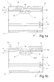
- IGBTs are electronic devices widely used in various electronic systems. IGBT devices of an advanced type, with low losses and small dimensions, for example of the type with trench-gate terminal or of a planar type (see, for example, Figures 1a and 1b ), are available on the market.
- Figure 1a shows, in cross-sectional view, a planar IGBT 1 of a known type, which comprises a substrate 2, made of silicon with a doping of a P++ type having a front side 2a and a back side 2b.
- a buffer layer 4 Formed on the front side 2a of the substrate 2 is a buffer layer 4, made of silicon of an N+ type, and formed on top of and in contact with the buffer layer 4 is a drift layer 6, made of silicon with a doping of an N- type.
- the drift layer 6 houses, at a top face 6a of its own, a body region 8, which extends in depth in the drift layer 6 starting from the top face 6a, and is formed by implantation of dopant species of a P type.
- a source region 10 is formed by implantation of dopant species of an N type, to form a region with N++ doping, which extends in the body region 8 starting from the top face 6a.
- the planar IGBT 1 further comprises a metal layer 12 formed on the top face 6a of the drift layer 6, in direct contact with the body region 8 and, partially, with the source region 10.
- the metal layer 12 is moreover separated from portions of the top face 6a that are external, in top plan view, to the body region 8 by means of layers of insulating material 14 and polysilicon 16 set on top of one another, in such a way that the polysilicon 16 is electrically insulated both from the top face 6a and from the metal layer 12 by the layers of insulating material 14.
- a gate region 18 of the planar IGBT 1 is thus formed.
- a collector terminal 19 made of metal material, is formed in direct electrical contact with the substrate 2.
- FIG. 1b shows a planar IGBT 20 similar to the planar IGBT 1 of Figure 1a (elements that are in common are designated by the same reference numbers).
- the planar IGBT 20 further comprises a barrier layer 22, formed by implantation of dopant species of an N type, which is formed in the drift layer 6 so as to surround the body region 8 externally and be in contact therewith.
- the potential that is set up between the barrier layer 22 and the body region 8 acts as a barrier in regard to the holes injected from the region 2 into the drift layer 6.
- the barrier layer 22 reduces the depletion area underneath the body region 8 and generates an accumulation of holes such as to decrease the resistivity of the respective portion of drift layer 6, and hence enables reduction of the saturation voltage V CEsat when the planar IGBT 20 is forward biased.
- the aim of the present invention is to provide an insulated gate semiconductor device, in particular an IGBT, and a manufacturing method thereof that will be able to overcome the drawbacks of the known art.
- an insulated gate semiconductor device in particular an IGBT, and a manufacturing method thereof are provided as defined in the annexed claims.
- the present invention regards an insulated gate bipolar transistor (IGBT) comprising: a semiconductor body having a front side and a back side opposite to one another; a drift region, which extends in the semiconductor body and has a first type of conductivity and a first doping value; a body region having a second type of conductivity, which extends in the semiconductor body and faces the front side of the semiconductor body; a barrier region having the first type of conductivity and a second doping value higher than the first doping value, which extends between the body region and the drift region in electrical contact with the body region and the drift region; and a buried region having the second type of conductivity, which extends in the drift region, at least partially aligned to the body region in a vertical direction substantially orthogonal to the front side and to the back side.
- IGBT insulated gate bipolar transistor
- said vertical direction is the direction of conduction of current of the IGBT.
- the body region houses a region that is a source of charge carriers having the first type of conductivity.
- a collector region which extends in an area corresponding to the back side of the semiconductor body in such a way that, in use, the current flows between the source region and the collector region.
- the semiconductor device is turned on by biasing a gate region, which extends in an area corresponding to the front side alongside the charge-carrier source region.
- the gate region can be, according to embodiments that are alternative to one another, formed on top of the front side (in this case the device is referred to as "planar”) or in such a way as to extend within the semiconductor body in a respective trench (in this case the device is referred to as "trench gate”).
- the buried region extends (in cross-sectional view and/or in plan view) alongside the gate region and vertically aligned to the body region, and is moreover separated from the body region by means of the barrier region.
- the buried region extends at a distance from the barrier region, at least partially aligned, in the vertical direction, to the body region.
- the barrier region is not present, and the buried region extends at a distance from the body region, at least partially aligned, in the vertical direction, to the body region.
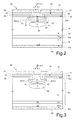
- FIG. 2 shows, in cross-sectional view, an insulated gate device, in particular an IGBT, designated by the reference number 30, according to one embodiment of the present invention.
- the IGBT device 30 is of a planar type and comprises a substrate 32, made of doped semiconductor material, for example of silicon with P++ doping having a value of resistivity ⁇ ⁇ 20 m ⁇ cm.
- the substrate 32 has a front side 32a and a back side 32b.
- Extending over the front side 32a of the substrate 32 is a buffer layer 34 made of doped semiconductor material, for example of silicon with N+ doping.
- the buffer layer 34 has a thickness of between approximately 1 ⁇ m and 50 ⁇ m, and a value of resistivity of between approximately 10 m ⁇ cm and 1 ⁇ cm.
- the buffer layer 34 is, for example, grown epitaxially on the substrate 32.
- a drift layer 36 Extending on top of the buffer layer 34 is a drift layer 36 made of doped semiconductor material, for example of silicon with N- doping (in which charge-carrier drift phenomena occur).
- the substrate 32, the buffer layer 34, and the drift layer 36 form a semiconductor body of the IGBT device 30.
- the drift layer 36 has a thickness of between approximately 10 ⁇ m and 150 ⁇ m, and a value of resistivity of between approximately 10 ⁇ cm and 100 ⁇ cm.
- the drift layer 36 is, for example, grown epitaxially on the buffer layer 34.
- the drift layer 36 houses, on its top face 36a, a body region 38, with P+ doping, which extends in depth in the drift layer 36 starting from the top face 36a.
- a source region 40 with N++ doping Extending within the body region 38, starting from the top face 36a, is a source region 40 with N++ doping. Moreover present is a barrier region 42, with N+ doping, which extends in the drift layer 36 so as to surround the body region 38 and be in electrical contact with the body region 38.
- the IGBT device 30 further comprises a buried region 44 (floating region), with a doping of a P type, which extends within the drift layer 36 substantially vertically aligned to the body region 38 and in electrical contact with the barrier region 42.
- the distance between the buried region 44 and the body region 38 is, according to one embodiment of the present invention, greater than 1 ⁇ m (for example, 2 ⁇ m) in order to guarantee, in use, the effect of hole barrier provided by the barrier region 42.
- the buried region 44 would have to be set at a maximum distance d max from the body region 38 (along the axis Z) not greater than 5 ⁇ m.
- the maximum distance d max is measured along the axis Z between the deepest point reached by the body region 38 and the starting point, once again along the axis Z, of the extension of the buried region 44, which will extend further along the axis Z throughout its thickness. Values of maximum distance d max between the body region 38 and the buried region 44 lower than 1 ⁇ m or higher than 5 ⁇ m are possible, but reduce the advantageous effects due to the presence of the buried region 44 (in particular on account of a deterioration of the breakdown voltage of the device).
- the barrier region 42 completely surrounds the body region 38 (obviously, underneath the top face 36a).
- the barrier region 42 only partially surrounds the body region 38; in particular, it extends between the buried region 44 and the body region 38, and not, in cross-sectional view, alongside the source region 40.
- the body region 38 extends in a horizontal direction (i.e., parallel to the plane XY) and vertically (i.e., in the direction defined by the axis Z).
- the buried region 44 extends in the drift layer 36 to a depth, measured along the axis Z, greater than the maximum depth reached by the body region 38.
- the buried region 44 is separated from the body region 38 by the barrier region 42, and is in contact with the barrier region 42.
- the buried region 44 is not in direct contact with the barrier region 42, but is separated therefrom by a portion of the drift layer 36.
- V CEsat saturation voltage
- the buried region 44 it is preferable not to separate the buried region 44 from the barrier region 42, or, in the case where they are separate, to keep them at a distance apart of less than approximately 5 ⁇ m.
- the body region 38 and the buried region 44 are at least partially aligned to one another, along the axis Z.
- the drift layer 36 has (in a way not shown in the figure) a surface-enhancement region, formed by implantation of phosphorus (for example, with a concentration of approximately 1 ⁇ 10 13 ions/cm 3 (in general, higher than the value of concentration of the drift layer 36).
- the IGBT device 30 further comprises a contact-terminal layer 46, made of conductive material, for example metal, which extends over the top face 36a of the drift layer 36, in direct contact with the body region 38 and, partially, with the source region 40.
- the contact-terminal layer 46 has, in use, the function of emitter contact of the IGBT device 30.
- the contact-terminal layer 46 is moreover separated from portions of the top face 36a that are external to the body region 38 by means of layers of insulating material and conductive material set on top of one another.
- a first insulating layer 48 for example made of silicon oxide (SiO 2 ) extends alongside the body region 38 on the top face 36a of the drift layer 36.
- an intermediate gate layer 50 for example made of polysilicon.
- a second insulating layer 52 extending on top of the intermediate gate layer 50 is a second insulating layer 52, made, for example, of borophosphosilicate glass (BPSG).
- BPSG borophosphosilicate glass
- the contact-terminal layer 46 Extending in fact on top of the second insulating layer 52 is the contact-terminal layer 46.
- an electrical contact (not shown in the figure) for biasing the gate terminal 54.
- collector-terminal layer 56 made of conductive material, for example metal.
- the IGBT device 30 In use, the IGBT device 30 having the structure described remains inhibited as long as the voltage between the gate terminal 54 and the emitter terminal 46 remains below a threshold value V TH of the IGBT device 30. In the inhibited state, the entire voltage between the collector terminal 56 and the emitter terminal 46 is withstood by the PN junction formed by the body region 38 and by the barrier layer 42/drift layer 36. When the voltage applied to the gate terminal 54 exceeds the threshold value V TH , the IGBT device 30 goes into the conduction state. The passage of current occurs in a vertical direction through the drift layer 36 (between the source region 40, biased by means of the emitter terminal 46, and the collector terminal 56), as indicated by the arrows 37 in Figure 2 .
- the direction of conduction of the IGBT device 30 is hence approximated as being substantially parallel to the direction defined by the axis Z (i.e., substantially orthogonal to the top face 36a of the structural layer 36 and to the back side 32b of the substrate 32).
- the current that passes is bipolar, i.e., the electrons travel from the source to the collector, traversing the channel region and the drift region, whilst the holes travel from the substrate 32 to the body region 38 where they re-close towards the metal 46.
- the present applicant has found that, in presence of the buried region 44, the electrical field that is generated, during use, in the IGBT device 30 has a profile different from that of the field generated in an IGBT device that is similar but without the buried region 44.
- the electrical field undergoes a variation of the slope at the buried region 44, the consequence of which is an increase of the breakdown voltage when the IGBT device is reversely biased.
- the IGBT device 30 hence has a breakdown voltage higher than IGBT devices of a known type.
- Figure 14 (illustrated hereinafter) shows, by way of example, the profile of the electrical field in the IGBT device 30 between the emitter terminal and the collector terminal (along the line of cross section I-I of Figure 2 ).
- FIG 3 shows an IGBT device 60 according to an embodiment alternative to the one illustrated in Figure 2 (however, elements that are in common are designated by the same reference numbers and not described any further).
- the embodiment of the IGBT device of Figure 3 differs from the one illustrated in Figure 2 in that the substrate 32 is of an N- type, and in that the body region 38, the source region 40, and the barrier region 42 extend in depth in the substrate 32 facing the front side 32a of the substrate 32.
- the buried region 44 is formed in the substrate 32, in an area corresponding to and, in lateral sectional view, underneath the body region 38 (the body region 38 and the buried region 44 are at least partially aligned to one another along the axis Z, and the buried region 44 extends to a depth, along the axis Z, greater than the maximum depth of the body region 38).
- the buried region 44 is in direct contact with the barrier region 42.
- the IGBT device 60 is then completed to form a first implanted region 61, of an N+ type, obtained by implantation of dopant species from the back side 32b of the substrate 32, to a depth of approximately 1.5 ⁇ m (said implanted region 61 having the same function as the buffer layer 34 of Figure 2 ), and to form a second implanted region 62, of a P++ type, by implantation of dopant species from the back side 32b of the substrate 32, said implanted region 62 extending facing the back side 32b between the surface of the back side 32b and the first implanted region 61.
- the IGBT device 30 and the IGBT device 60 operate in a way similar to one another, and in particular share the same advantages deriving from the presence of the buried region 44.
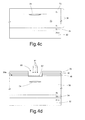
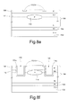
- Figures 4a-4f show steps of a manufacturing method that can be used for producing the IGBT device 30 of Figure 2 .
- the substrate 32 of a P++ doped type, of monocrystalline silicon is provided. Then, a first step of epitaxial growth is carried out on the front side 32a of the substrate 32.
- the epitaxial growth is performed in a controlled environment, for example with the chemical-vapour-deposition (CVD) technique, by depositing vapour of silicon and phosphorus, to form the buffer layer 34 (which, as has been said, is doped N+ with a dose of between approximately 1 ⁇ 10 15 and 1 ⁇ 10 18 ions/cm 2 ).
- the buffer layer 34 has a thickness of between approximately 1 ⁇ m and 50 ⁇ m.
- a second step of epitaxial growth is carried out on the buffer layer 34, for example with the CVD technique, depositing vapours of silicon and phosphorus, to form a first intermediate drift layer 73 (which, as has been said, is doped N- with a dose of between approximately 5 ⁇ 10 13 and 5 ⁇ 10 14 ions/cm 2 ).
- the first intermediate drift layer 73 has a thickness of between approximately 10 ⁇ m and 150 ⁇ m.
- a photoresist mask 70 is formed on the top side 73a of the first intermediate drift layer 73, and, by means of the photolithographic process, an opening 71 is defined in the region in which it is desired to form the buried region 44 of Figure 2 , exposing a portion of the top side 73a of the first intermediate drift layer 73.
- the opening 71 has a shape and width chosen according to the need, for example, in top plan view, a quadrangular shape with sides (opening of the photomask) of between approximately 0.5 ⁇ m and 5 ⁇ m.
- a step of implantation of dopant species of a P type is carried out (as represented schematically in Figure 4b by the arrows 72) to form in the first intermediate drift layer 73 an implanted region 74.
- the implantation dose is between approximately 1 ⁇ 10 12 and 1 ⁇ 10 14 ions/cm 2 , with an implantation energy of between approximately 80 keV and 1 MeV.
- the implantation step is followed by a step of epitaxial growth of silicon with N- doping on top of the first intermediate drift layer 73 to form a second intermediate drift layer 76 having a dose of doping and a type of dopant approximately the same as the first intermediate drift layer 73.
- the second intermediate drift layer 76 has a thickness of between approximately 3 ⁇ m and 12 ⁇ m, preferably approximately 7 ⁇ m.
- the first drift layer 73 and the second drift layer 76 form the drift layer 36 of Figure 2 .
- a step of surface enhancement is then carried out by implantation of dopant species of an N type on a surface portion of the second intermediate drift layer 76.
- Said step of surface enhancement comprises, for example, implanting phosphorus ions (with an implantation energy of between approximately 50 and 200 keV and a dose of between approximately 0.5 ⁇ 10 12 0.5 ⁇ 10 13 ions/cm 2 ).
- a step of deposition of insulating material for example silicon oxide (SiO 2 ), is carried out on the top side 36a of the drift layer 36 to form the first insulating layer 48.
- the first insulating layer 48 has, for example, a thickness of between approximately 30 nm and 1000 nm.
- a step of deposition of polysilicon is carried out on the first insulating layer 48 to form the intermediate gate layer 50, for example having a thickness of between approximately 100 nm and 1000 nm.
- a photoresist layer 79 formed on the intermediate gate layer 50 is a photoresist layer 79, and, by means of the photolithographic process, an opening 80 is defined in the photoresist layer 79 to expose a portion of the intermediate gate layer 50.
- the opening 80 is formed in the region of the drift layer 36 in which it is desired to form the body region 38, and is at least partially aligned to the implanted region 74.
- the opening 80 has, in top plan view, a for example quadrangular shape, with sides having the same length as one another or different lengths, for example of between approximately 1 ⁇ m and 10 ⁇ m. Any other shape for the opening 80 is, however, possible, according to the desired layout.
- a step of etching of the intermediate gate layer 50 is then carried out, for example using nitric acid and hydrofluoric acid (HNO 3 +HF), to expose the first insulating layer 48.
- This is followed by a step of etching of the first insulating layer 48, for example using hydrofluoric acid, to expose a corresponding surface portion of the drift layer 36.
- a step of implantation (represented schematically by the arrows 81) of dopant species of an N type, for example phosphorus, with a dose of between approximately 1 ⁇ 10 12 and 1 ⁇ 10 13 ions/cm 2 and with an energy of between 80 keV and 1 MeV, forms an implanted region 82 within the drift layer 36.
- dopant species of an N type for example phosphorus
- a step of thermal treatment is carried out so as to diffuse the implanted dopant species adequately (implanted regions 74 and 82). In this way, the buried region 44, with P doping, and the barrier region 42, with N+ doping, are formed.
- a new implantation is carried out (represented schematically by the arrows 83) of dopant species of a P type, for example boron, with a dose of between approximately 1 ⁇ 10 13 and 1 ⁇ 10 16 ions/cm 2 and an implantation energy of between approximately 50 keV and 200 keV at the opening 80 previously formed.
- a subsequent step of thermal diffusion leads to formation of the body region 38, of a P+ type.
- BPSG borophosphosilicate glass
- the layer of borophosphosilicate glass is deposited in a known way and selectively removed at the body region 38 to form an opening designed to enable subsequent electrical contact between the body region 38 and the contact-terminal layer 46.
- a metal layer is deposited on the second insulating layer 52 and in contact with the body layer 38 so as to form the contact-terminal layer 46.
- a metal-contact layer is deposited also on the back side 32b of the substrate 32 to obtain the IGBT device 30 of Figure 2 .
- the IGBT device 60 of Figure 3 and in particular the buried region 44, is formed in a way similar to what has been described with reference to Figures 4a-4f .
- the body region and the buried region 44 are formed, as has already been said, in the substrate. Consequently, the steps of epitaxial growth on the substrate are not necessary. Steps of implantation of dopant species from the back side 32b of the substrate 32 are, instead, envisaged to form the first and second implanted regions 61, 62.
- the first implanted region 61 is formed, for example, by means of an implantation of phosphorus.
- the second implanted region 62 is formed, for example, by means of an implantation of boron.
- FIG. 5 shows an IGBT device 90 according to a further embodiment of the present invention.
- the IGBT device 90 of Figure 5 is similar to the IGBT device 30 of Figure 2 .
- Elements that are in common between the IGBT device 90 of Figure 5 and the IGBT device 30 of Figure 2 are designated by the same reference numbers and will not be described any further.
- the IGBT device 90 differs from the IGBT device 30 owing to the presence of a barrier layer 92, made of a semiconductor material (for example silicon) with an N doping, which extends on the top side 36a of the drift layer 36.
- the barrier layer 92 is made of silicon with N+ doping.
- the barrier layer 92 surrounds the body region 38 and separates the latter from the buried region 94 and has the same function as the barrier region 42 of the IGBT device 30 of Figure 2 .
- the buried region 94 extends at the interface between the drift layer 36 and the barrier layer 92, in part in the drift layer 36 and in part in the barrier layer 92.
- Figure 6 shows an intermediate step of manufacture of the IGBT device 90 of Figure 5 .
- Figure 6 shows the IGBT device 90 following upon manufacturing steps similar to those described with reference to Figures 4a and 4b , and to further steps described hereinafter.
- a step is carried out of epitaxial growth of semiconductor material (e.g., silicon) on the top side 73a of the first intermediate drift layer 73.
- semiconductor material e.g., silicon
- the epitaxial growth is obtained by deposition of vapours of silicon and phosphorus ions, to form an epitaxial layer of silicon with a doping of an N type.
- the level of concentration of dopant in the barrier layer 92 thus formed is between approximately 1 ⁇ 10 15 and 1 ⁇ 10 16 ions/cm 3 , to obtain a value of resistivity of the barrier layer 92 of between approximately 0.5 and 5 ⁇ cm.
- the thickness of the barrier layer 92 is between approximately 3 ⁇ m and 12 ⁇ m. Structurally, the barrier layer 92 is similar to the second intermediate drift layer 76 described with reference to Figure 4c .
- the step of epitaxial growth (which is carried out typically at a temperature of approximately 1200°C) is already sufficient to cause a partial diffusion of the implanted region 74.
- the IGBT device 90 of Figure 5 can be alternatively formed according to what has been described with reference to the IGBT device 60 of Figure 3 .
- the body region 38 and the buried region 94 are formed in the substrate 32, and just one step of epitaxial growth is present, in particular to form the barrier layer 92 according to what has already been described.
- steps of implantation of dopant species from the back side 32b of the substrate 32 to form appropriately doped implanted regions an N+ region having the function of the buffer layer 34, and a P++ region facing the back side 32b of the substrate 32).
- the present invention likewise applies to IGBT devices of a type with trench-gate terminal.
- FIG. 7 shows an IGBT device 100 with trench-gate terminal, according to one embodiment of the present invention.
- the IGBT device 100 comprises a substrate 102, made of doped semiconductor material, for example of silicon with P++ doping having a value of resistivity ⁇ ⁇ 20 mQ ⁇ cm.
- the substrate 102 has a front side 102a and a back side 102b.
- Extending on the front side 102a of the substrate 102 is a buffer layer 104 made of doped semiconductor material, for example silicon with N+ doping.
- the buffer layer 104 has a thickness of between approximately 1 ⁇ m and 50 ⁇ m, and a value of resistivity of between approximately 10 m ⁇ cm and 1 ⁇ cm.
- the buffer layer 104 is, for example, grown epitaxially on the substrate 102.
- a structural layer 106 made of doped semiconductor material, for example silicon with N- doping.
- the structural layer 106 has a thickness of between approximately 10 ⁇ m and 150 ⁇ m, and a value of resistivity of between approximately 10 ⁇ cm and 100 ⁇ cm.
- the structural layer 106 is, for example, grown epitaxially on the buffer layer 104.
- the structural layer 106 houses, on a top face 106a of its own, a body region 108, with P doping, which extends in depth in the structural layer 106 starting from the top face 106a. Extending underneath the body region 108 and in contact therewith is a barrier region 112 with N+ doping. The barrier region 112 separates the body region 108 from the rest of the structural layer 106, which assumes the function of drift region 106'.
- source regions 113 with N+ doping, which extend into the structural layer 106 within the body region 108 and facing the top face 106a of the structural layer 106.
- the IGBT device 100 further comprises gate regions 116 formed in respective trenches, which extend in the structural layer 106 from the top face 106a to the substrate 102.
- Each trench housing a gate region 116 has a depth greater than the thickness of the body region 108 and of the barrier region 112, and in any case smaller than the thickness of the structural layer 106.
- Each gate region 116 comprises an insulating portion 116a and a conductive portion 116b, arranged with respect to one another in such a way that the conductive portion 116b is insulated from the structural layer 106 by means of the insulating portion 116a.
- the IGBT device 100 further comprises a buried region 114 with a doping of a P type, which extends within the structural layer 106 in electrical contact with the barrier region 112.
- the distance between the body region 108 and the buried region 114 is preferably between 1 ⁇ m and 5 ⁇ m.
- the buried region 114 is arranged facing a side portion of a respective gate region 116, at least partially aligned, along the axis Z, to the body region 108 set in a position corresponding to the same side portion of the respective gate region 116.
- the buried region 114 is set between the two gate regions 116 facing one another.
- the extension in depth into the structural layer 106 of the gate regions 116 and of the buried region 114 is such that the extension in depth of the gate regions 116 is equal to or greater than the extension in depth of the buried region 114.
- the maximum depth reached by the buried region 114 in the structural layer 106, in the positive direction of the axis Z is equal to or less than the maximum depth reached by the gate region 116 in the structural layer 106 in the positive direction of the axis Z.
- the IGBT device 100 further comprises a contact-terminal layer 118, made of conductive material, for example metal, which extends over the top face 106a of the structural layer 106, in direct contact with the body region 108 and, at least partially, with the source regions 113.
- the contact-terminal layer 118 has, in use, the function of emitter contact of the IGBT device 100.
- the contact-terminal layer 118 is moreover separated from the portions of the gate regions 116 that face the top side 106a of the structural layer 106 by means of respective insulation regions 120, for example made of borophosphosilicate glass (BPSG), each formed on top of a respective gate region 116.
- respective insulation regions 120 for example made of borophosphosilicate glass (BPSG), each formed on top of a respective gate region 116.
- BPSG borophosphosilicate glass
- collector-terminal layer 122 made of conductive material, for example metal.
- the IGBT device 100 operates in a way similar to what has already been described with reference to the IGBT device 30 (with the evident differences due to the trench-gate terminal).
- the path of the current between the emitter terminal 118 and the collector terminal 122 is represented graphically by the arrows 137 and is substantially parallel to the direction defined by the axis Z (i.e., substantially orthogonal to the top face 106a of the structural layer 106 and to the back side 102b of the substrate 102).
- the substrate 102 with a P++ doping is provided, made of monocrystalline silicon. Then, a first step of epitaxial growth is carried out on the front side 102a of the substrate 102.
- the epitaxial growth is performed in a controlled environment, for example using the chemical-vapour-deposition (CVD) technique, depositing vapours of silicon and phosphorus to form the buffer layer 104 (which, as has been mentioned previously, is doped N+ with a dose of between approximately 1 ⁇ 10 15 and 1 ⁇ 10 18 ions/cm 2 ).
- the buffer layer 104 has a thickness of between approximately 1 ⁇ m and 50 ⁇ m.
- a second step of epitaxial growth is carried out on the buffer layer 104, for example with the CVD technique, depositing vapours of silicon and phosphorus to form the drift region 106' (which is doped N- with a dose of between approximately 5 ⁇ 10 13 and 5 ⁇ 10 14 ions/cm 2 ).
- the drift region 106' has a thickness of between approximately 10 ⁇ m and 150 ⁇ m.
- a photoresist mask 127 is formed on the top side of the intermediate drift region 106' and, using the photolithographic process, an opening is defined in the region where it is desired to form the buried region 114 of Figure 7 , exposing a portion of the top side of the drift region 106'.
- Said opening has a shape and a width chosen according to the need, for example having in top plan view a quadrangular shape with a width of the photomask of between approximately 0.5 ⁇ m and 5 ⁇ m. Other shapes and other dimensions are, however, possible, according to the specific design requirements.
- a step of implantation of dopant species of a P type is then carried out to form an implanted region 130 in the drift region 106'.
- the implantation dose is, according to one embodiment of the present invention, between approximately 1 ⁇ 10 12 and 1 ⁇ 10 14 ions/cm 2 , with an implantation energy of between approximately 80 keV and 1 MeV.
- the implantation step is followed by a step of epitaxial growth of silicon with N- doping or, alternatively, not doped, on the drift region 106', to form an intermediate structural layer 132.
- the intermediate structural layer 132 has a thickness of between approximately 3 ⁇ m and 12 ⁇ m.
- the drift region 106' and the intermediate structural layer 132 form the structural layer 106 of Figure 7 .
- an implantation (represented schematically by arrows 133) of dopant species of an N type (for example, phosphorus) is carried out in the structural layer 106, to form an implanted region 134.
- the implantation dose is between approximately 1 ⁇ 10 12 and 1 ⁇ 10 13 ions/cm 2 , with an implantation energy of between approximately 80 keV and 1 MeV.
- the implantation of Figure 8 is performed only in the active area of the device, using an appropriate mask. This approach is important in order to prevent doping of edge regions of the IGBT device 100, outside the active area.
- a thermal process is then carried out ( Figure 8c ) to favour diffusion of the dopant species of the implanted regions 130 and 134.
- the diffusion of the dopant species of the implanted gate region 130 leads to formation of the buried region 114, whereas the diffusion of the dopant species of the implanted gate region 134 leads to formation of the barrier region 112.
- a further implantation of dopant species of a P type in the active area in particular within the region N+ that has formed following upon diffusion of the dopant species of the implanted region 134
- a subsequent thermal treatment to enable diffusion of the dopant, form the body region 108.
- Implantation of the dopant species of a P type to form the body region 108 comprises an implantation dose of between 1 ⁇ 10 13 and 1 ⁇ 10 14 ions/cm 2 with an implantation energy of between 80 keV and 1 MeV.
- the next step is formation of the IGBT device 100.
- the source regions 113 are formed within the body region 108 by implantation of dopant species of an N type and a subsequent thermal process of diffusion.
- the source regions 113 have, in top plan view, a shape that is, for example, circular or quadrangular (even though any other shape is possible) and is formed in such a way as to surround, in top plan view, a respective gate region 116.
- the drift layer 106 is selectively etched so as to form trenches 140, which extend from the top face 106a of the structural layer 106 to the substrate 102.
- the depth of the trenches 140 in the structural layer 106 is equal to or greater than the maximum depth at which the buried region 114 is found.
- Each trench 140 is formed, for example, by dry etching, for example using a reactive-ion-etching (RIE) technique or a deep-reactive-ion-etching (DRIE) technique.
- RIE reactive-ion-etching
- DRIE deep-reactive-ion-etching
- a step of deposition of a layer of insulating material, for example silicon oxide grown thermally, is then carried out so as to form, adjacent to the inner walls and to the bottom of each trench 140, the respective insulating portion 116a.
- a layer of insulating material for example silicon oxide grown thermally
- each trench 140 is filled to form the respective conductive portion 116b in each trench 140.
- the IGBT device 100 is finally completed to form portions of BPSG on the conductive portions 116b so as to insulate them from outside, to form the contact-terminal layer 118, made of conductive material, for example by deposition of metal, and to form the collector-terminal layer 122 on the back side 102b of the substrate 102, for example by deposition of conductive material, such as metal.
- the IGBT device 100 of Figure 7 is thus obtained.
- the substrate 102 is of an N- type.
- the layer with N+ doping, which forms the buffer layer 104, and the layer with P++ doping set between the buffer layer 104 and the collector-terminal layer 122 are formed by implantation of dopant species (respectively N and P) from the back side 102b of the substrate 102.
- dopant species respectively N and P
- FIG. 9 shows an IGBT device 150 according to a further embodiment of the present invention.
- the IGBT device 150 is of a trench-gate-terminal type.
- the IGBT device 150 of Figure 9 differs from the IGBT device 100 of Figure 7 in that the barrier layer (designated by the reference 112 in Figure 7 ) is not formed by implantation but is a layer grown epitaxially and doped N+ during the step of epitaxial growth. The body region of the IGBT device is consequently formed in said epitaxial layer.
- the process of manufacture of the IGBT device 150 is described more fully with reference to Figures 10a and 10b .
- elements of the IGBT device 150 that are in common with those of the IGBT device 100 are designated by the same reference numbers and will not be described any further.
- FIG 10a shows the IGBT device 150 during an intermediate manufacturing step, and in particular following upon the manufacturing steps already described with reference to Figure 8a and upon further steps described hereinafter.
- the substrate 102 is provided, on which the buffer layer 104 and the drift region 106' are formed. Then, implantation of P dopant species is carried out to form the implanted region 130.
- an intermediate structural layer 152 is formed on the drift region 106'.
- the intermediate structural layer 152 differs from the intermediate structural layer 132 of Figure 8a in that it has a doping of an N+ type.
- the intermediate structural layer 152 is formed, for example, by means of epitaxial growth of silicon in an environment with the presence of vapours of silicon and phosphorus, or other appropriate dopant species of an N type.
- the intermediate structural layer of Figure 10a has a doping level of between approximately 1 ⁇ 10 15 and 1 ⁇ 10 16 ions/cm 3 , so as to obtain a value of resistivity of between approximately 0.5 and 5 ⁇ cm.
- the thickness of the second intermediate drift layer 152 is between approximately 3 and 12 ⁇ m.
- the implanted region 130 undergoes a partial diffusion.
- an implantation of dopant species of a P type is carried out in the active area of the IGBT device 150, and a subsequent thermal process for favouring diffusion thereof.
- the implantation step comprises implanting boron ions, with an implantation dose of between approximately 1 ⁇ 10 14 and 1 ⁇ 10 15 ions/cm 2 and an implantation energy of 80 keV-1 MeV.
- a body region 156 (with P doping), and a barrier layer 158 (with N+ doping) are formed set between and in electrical contact with the body region 156 and the buried region 114.
- the IGBT device 150 of Figure 9 is thus formed.
- the buffer layer 104 (with N+ doping) can be obtained by implantation of dopant species of an N type on the top side 102a of the substrate 102.
- the P++ doping of the substrate 102 can be obtained by implantation of dopant species of a P type.
- the starting substrate 102 has an N- doping.
- IGBT devices 30, 60, 100, and 150 can be integrated in a single chip.
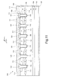
- Figure 11 shows a chip or die 200 comprising a plurality of IGBT devices 150.
- the chip 200 of Figure 11 comprises a plurality of gate regions 116 and a respective plurality of source regions 113. Extending alongside each gate region 116 is a buried region 114 of the type described previously.
- IGBT devices 150 of Figure 11 can be replaced, in a way evident to the person skilled in the branch, by IGBT devices 30, 60, 90, or 100 according to any other of the embodiments described previously.
- Figure 12 shows an edge region 245 of a chip 249 comprising one or more IGBT devices 90 according to the embodiment of Figure 5 (elements that are in common are designated by the same reference numbers).
- the edge region 245 is a region of the chip 249 outside the active area 251 of the IGBT devices 90, in which the body and source regions are formed.
- Figure 12 shows, in the edge region 245, a gate-contact terminal 255 for biasing the gate terminals in a known way.
- Figure 12 shows an edge-termination structure used, in general, when the formation of the barrier layer with N+ doping (for example, the barrier layer 92 of Figure 5 ) extends beyond the active area 251 of the IGBT device, creating an electrical connection between the active area 251 and regions outside the active area 251.
- the barrier layer with N+ doping for example, the barrier layer 92 of Figure 5
- Figure 12 shows an edge-termination structure used, in general, when the formation of the barrier layer with N+ doping (for example, the barrier layer 92 of Figure 5 ) extends beyond the active area 251 of the IGBT device, creating an electrical connection between the active area 251 and regions outside the active area 251.
- This situation arises, for example, in the case of an IGBT device obtained according to the embodiment of Figure 5 (i.e., the IGBT device is of a planar type and comprises a barrier layer 92 grown epitaxially).
- the edge structure described is not, however, limited to said embodiment.
- the edge-termination structure 250 comprises, according to a first embodiment, an edge ring 254, which extends into the barrier layer 92 facing a top side 92a of the barrier layer 92.
- the edge ring 254 is formed by implantation of dopant species of a P type, for example simultaneously with formation of the body regions 38.
- at least one implanted well 256 is present at the interface between the drift layer 36 and the barrier layer 92, in a position corresponding to the portion of the barrier layer 92 in which the edge ring 254 extends, is at least one implanted well 256 (two implanted wells 256 are illustrated in Figure 12 ).
- the implanted wells 256 are similar to the buried region 94 and are for example formed simultaneously with formation of the buried regions 94.
- the implantation dose and energy for formation of the edge ring 254 are chosen in such a way that, during the step of diffusion of the implanted dopant species, the edge ring 254 and the implanted wells 256 extend into the barrier layer 92 until they come into contact with one another. In this way, a charge region P is formed inside the barrier layer 92, which interrupts the path of possible charge carriers of an N type that flow from the active area 251 to the edge of the chip 252.
- FIG 13 shows an edge-termination structure 301 of a chip 300 comprising one or more IGBT devices 90, according to an embodiment alternative to what has been described with reference to Figure 12 (however, elements that are in common with what is illustrated in Figure 12 are designated by the same reference numbers).
- the edge ring 254 is replaced by a plurality of edge rings 302.
- each edge ring 302 has a spatial extension that is approximately the same as the spatial extension of the implanted wells 256.
- each edge ring 302 is formed in a position corresponding to and at least partially aligned (in top plan view) with a respective implanted well 256.
- Each of the edge rings 302 is formed in a way similar to what has already been described with reference to the edge ring 254. In this way, during the step of diffusion of the implanted dopant species, the edge rings 302 and the implanted wells 256 come into contact with one another to form a respective plurality of charge regions P inside the barrier layer 92 that interrupt the path of possible charge carriers of an N type that flow from the active area 251 to the edge of the chip 300.
- the present invention irrespective of the particular embodiment of the IGBT device, makes it possible to obtain an increase in the breakdown voltage.
- the curve 350 of Figure 14 shows the profile of the electrical field that is set up between the emitter terminal 46 and the collector terminal 56 within the active area of the IGBT device 30, from the top side 36a of the drift layer 36 ( Figure 2 ) to the substrate 32.
- the reversal of the slope of the curve corresponds to the depth at which the buried region 44 is located. It is evident that a similar curve can be obtained for all the IGBT devices described according to the embodiments of the present invention and not only for the IGBT device 30 of Figure 2 (reference to which has been used herein merely for greater clarity of exposition).
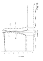
- the present invention also affords an advantage as regards the energy off of the IGBT device.
- Figure 15 shows switching-off curves E1 and E2 for an IGBT device according to the present invention (for example, the IGBT device 30 of Figure 2 ) and switching-off curves E3 and E4 for an IGBT device of a known type, for example of the type shown in Figure 1b .
- the curve E1 rises more rapidly than the respective curve E3.
- the curve E2 drops more rapidly than the respective curve E4.
- the curves E1 and E2 represent respectively the voltage V CE and the current Ic of the IGBT device 30 of Figure 2
- the curves E3 and E4 represent respectively the voltage V CE and the current Ic of the IGBT device of Figure Ib (of a known type).
- the area subtended by the curve El in the time interval t E1 -t M' added to the area subtended by the curve E2 in the time interval t M' -t E2 is smaller than the area subtended by the curve E3 in the time interval t E3 - tM " added to the area subtended by the curve E4 in the time interval t M "-t E4 , which hence means lower energy dissipation for each individual switching.
- the instant t E1 is substantially the instant at which the curve E1 starts to rise, and corresponds approximately to the instant t E3 , at which also the curve E3 starts to rise. Instead, the instants t E2 and t E4 are, respectively, the instants at which the curves E2 and E4 reach a substantially stable value.
- the instant t M' is the instant of intersection between the curve E1 and the curve E2; the instant t M " is the instant of intersection between the curve E3 and the curve E4.
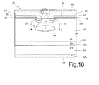
- the present applicant has found that the presence of a buried region (for instance, the buried region 44 described with reference to Figure 2 ) affords an advantage in terms of improvement (increase in the breakdown voltage) also in the case of IGBT devices without a barrier region that surrounds the body region (for example, in IGBT devices of the type illustrated in Figure 1a ).
- the present invention must consequently be understood as extending to IGBT devices 400 of the type illustrated, by way of example, in Figure 16 .
- the IGBT device 400 of Figure 16 is similar to the IGBT device 30 of Figure 2 (elements that are in common are designated by the same reference numbers). However, what has been described with reference to Figure 16 is immediately applicable to the embodiments of Figures 3 , 7 , and 9 , in a way that will be evident to the person skilled in the branch.
- the IGBT device 400 differs from the IGBT device 30 in that it does not comprise the barrier region 42.
- the buried region 44 consequently extends in the drift region 36 at a distance from the body region 38, for example at a distance of between approximately 1 ⁇ m and 5 ⁇ m.
- the semiconductor regions of a P type can be replaced by respective regions of an N type, and consequently the semiconductor regions of an N type can be replaced by respective regions of a P type.
- the regions described as insulating regions can be made of any insulating material, for example silicon nitride, TEOS, etc.
- semiconductor material such as silicon for the formation of the IGBT devices according to the present invention
- semiconductor material such as silicon for the formation of the IGBT devices according to the present invention
- other types of semiconductor material can be used, for example silicon carbide, gallium nitride, gallium arsenide, and others still.
Landscapes
- Electrodes Of Semiconductors (AREA)
- Metal-Oxide And Bipolar Metal-Oxide Semiconductor Integrated Circuits (AREA)
Abstract
Description
- The present invention relates to an insulated gate semiconductor device and to a manufacturing method thereof. In particular, the present invention regards an insulated gate bipolar transistor (IGBT) with optimized breakdown voltage.
- IGBTs are electronic devices widely used in various electronic systems. IGBT devices of an advanced type, with low losses and small dimensions, for example of the type with trench-gate terminal or of a planar type (see, for example,
Figures 1a and 1b ), are available on the market. -
Figure 1a shows, in cross-sectional view, a planar IGBT 1 of a known type, which comprises asubstrate 2, made of silicon with a doping of a P++ type having afront side 2a and aback side 2b. - Formed on the
front side 2a of thesubstrate 2 is abuffer layer 4, made of silicon of an N+ type, and formed on top of and in contact with thebuffer layer 4 is adrift layer 6, made of silicon with a doping of an N- type. Thedrift layer 6 houses, at atop face 6a of its own, abody region 8, which extends in depth in thedrift layer 6 starting from thetop face 6a, and is formed by implantation of dopant species of a P type. Within the body region 8 asource region 10 is formed by implantation of dopant species of an N type, to form a region with N++ doping, which extends in thebody region 8 starting from thetop face 6a. The planar IGBT 1 further comprises ametal layer 12 formed on thetop face 6a of thedrift layer 6, in direct contact with thebody region 8 and, partially, with thesource region 10. Themetal layer 12 is moreover separated from portions of thetop face 6a that are external, in top plan view, to thebody region 8 by means of layers ofinsulating material 14 andpolysilicon 16 set on top of one another, in such a way that thepolysilicon 16 is electrically insulated both from thetop face 6a and from themetal layer 12 by the layers ofinsulating material 14. Agate region 18 of the planar IGBT 1 is thus formed. Finally, on theback side 2b of thesubstrate 2 acollector terminal 19, made of metal material, is formed in direct electrical contact with thesubstrate 2. -
Figure 1b shows aplanar IGBT 20 similar to the planar IGBT 1 ofFigure 1a (elements that are in common are designated by the same reference numbers). The planar IGBT 20 further comprises abarrier layer 22, formed by implantation of dopant species of an N type, which is formed in thedrift layer 6 so as to surround thebody region 8 externally and be in contact therewith. - In use, the potential that is set up between the
barrier layer 22 and thebody region 8 acts as a barrier in regard to the holes injected from theregion 2 into thedrift layer 6. This results in an operative advantage during use of theplanar IGBT 20, in so far as the portion of thedrift layer 6 close to thebody region 8 can be modulated in a more effective way as compared to the planar IGBT 1 ofFigure 1a . Thebarrier layer 22 reduces the depletion area underneath thebody region 8 and generates an accumulation of holes such as to decrease the resistivity of the respective portion ofdrift layer 6, and hence enables reduction of the saturation voltage VCEsat when theplanar IGBT 20 is forward biased. - According to this embodiment, however, since the concentration of spatial charge underneath the
barrier layer 22 is high, in conditions of reverse biasing the breakdown voltage decreases. Said reduction in the breakdown voltage can be compensated by modulating the thickness and resistivity of thedrift layer 6. This solution, albeit guaranteeing an adequate breakdown voltage, does not guarantee optimal values of the "energy off" (energy consumption at turning-off of the device) and of the peak electrical field underneath thebody region 8. A very high electrical field could cause breakdown of the device during the reliability tests. In other words, when the device is in extreme working conditions (high humidity and/or high temperature in conditions of reverse biasing), very high localized electrical fields (i.e., ones well above the critical electrical field of silicon) can cause undesirable and unexpected breakdown. - The aim of the present invention is to provide an insulated gate semiconductor device, in particular an IGBT, and a manufacturing method thereof that will be able to overcome the drawbacks of the known art.
- According to the present invention an insulated gate semiconductor device, in particular an IGBT, and a manufacturing method thereof are provided as defined in the annexed claims.
- In particular, the present invention regards an insulated gate bipolar transistor (IGBT) comprising: a semiconductor body having a front side and a back side opposite to one another; a drift region, which extends in the semiconductor body and has a first type of conductivity and a first doping value; a body region having a second type of conductivity, which extends in the semiconductor body and faces the front side of the semiconductor body; a barrier region having the first type of conductivity and a second doping value higher than the first doping value, which extends between the body region and the drift region in electrical contact with the body region and the drift region; and a buried region having the second type of conductivity, which extends in the drift region, at least partially aligned to the body region in a vertical direction substantially orthogonal to the front side and to the back side. In particular, said vertical direction is the direction of conduction of current of the IGBT. In greater detail, the body region houses a region that is a source of charge carriers having the first type of conductivity. Moreover present is a collector region, which extends in an area corresponding to the back side of the semiconductor body in such a way that, in use, the current flows between the source region and the collector region. As is known, the semiconductor device is turned on by biasing a gate region, which extends in an area corresponding to the front side alongside the charge-carrier source region. The gate region can be, according to embodiments that are alternative to one another, formed on top of the front side (in this case the device is referred to as "planar") or in such a way as to extend within the semiconductor body in a respective trench (in this case the device is referred to as "trench gate"). In greater detail, irrespective of the embodiment, the buried region extends (in cross-sectional view and/or in plan view) alongside the gate region and vertically aligned to the body region, and is moreover separated from the body region by means of the barrier region. According to a further embodiment of the present invention, the buried region extends at a distance from the barrier region, at least partially aligned, in the vertical direction, to the body region. According to another embodiment of the present invention, the barrier region is not present, and the buried region extends at a distance from the body region, at least partially aligned, in the vertical direction, to the body region.
- For a better understanding of the present invention, preferred embodiments thereof are now described, purely by way of nonlimiting example and with reference to the attached drawings, wherein:
-
Figures 1a and 1b show respective IGBTs of a known type; -
Figure 2 shows, in cross-sectional view, an IGBT of a planar type according to one embodiment of the present invention; -
Figure 3 shows, in cross-sectional view, an IGBT of a planar type according to a further embodiment of the present invention; -
Figures 4a-4f show successive steps of a process of manufacture of the IGBT ofFigure 2 ; -
Figure 5 shows, in cross-sectional view, an IGBT of a planar type according to a further embodiment of the present invention; -
Figure 6 shows the IGBT ofFigure 5 in an intermediate manufacturing step; -
Figure 7 shows, in cross-sectional view, an IGBT of a type with trench-gate terminal according to one embodiment of the present invention; -
Figures 8a-8f show successive steps of a process of manufacture of the IGBT ofFigure 7 ; -
Figure 9 shows, in cross-sectional view, an IGBT of a type with trench-gate terminal according to a further embodiment of the present invention; -
Figures 10a and 10b show intermediate steps of manufacture of the IGBT ofFigure 9 ; -
Figure 11 shows, in cross-sectional view, a chip comprising a plurality of IGBT devices ofFigure 9 ; -
Figure 12 shows, in cross-sectional view, an embodiment of an edge-termination structure of a chip comprising one or more IGBT devices formed according to the embodiment ofFigure 5 ; -
Figure 13 shows a further embodiment of an edge-termination structure of a chip comprising one or more IGBT devices formed according to the embodiment ofFigure 5 ; -
Figure 14 is a curve of intensity of electrical field as the distance from the surface of an IGBT varies, according to the present invention; -
Figure 15 shows energy-off curves of an IGBT device according to the present invention as compared to an IGBT device of a known type; and -
Figure 16 shows, in cross-sectional view, an IGBT of a planar type according to a further embodiment of the present invention. -
Figure 2 shows, in cross-sectional view, an insulated gate device, in particular an IGBT, designated by thereference number 30, according to one embodiment of the present invention. - The
IGBT device 30 is of a planar type and comprises asubstrate 32, made of doped semiconductor material, for example of silicon with P++ doping having a value of resistivity ρ ≤ 20 mΩ·cm. Thesubstrate 32 has afront side 32a and aback side 32b. Extending over thefront side 32a of thesubstrate 32 is abuffer layer 34 made of doped semiconductor material, for example of silicon with N+ doping. Thebuffer layer 34 has a thickness of between approximately 1 µm and 50 µm, and a value of resistivity of between approximately 10 mΩ·cm and 1 Ω·cm. Thebuffer layer 34 is, for example, grown epitaxially on thesubstrate 32. Extending on top of thebuffer layer 34 is adrift layer 36 made of doped semiconductor material, for example of silicon with N- doping (in which charge-carrier drift phenomena occur). Thesubstrate 32, thebuffer layer 34, and thedrift layer 36 form a semiconductor body of theIGBT device 30. Thedrift layer 36 has a thickness of between approximately 10 µm and 150 µm, and a value of resistivity of between approximately 10 Ω·cm and 100 Ω·cm. Thedrift layer 36 is, for example, grown epitaxially on thebuffer layer 34. Thedrift layer 36 houses, on itstop face 36a, abody region 38, with P+ doping, which extends in depth in thedrift layer 36 starting from thetop face 36a. Extending within thebody region 38, starting from thetop face 36a, is asource region 40 with N++ doping. Moreover present is abarrier region 42, with N+ doping, which extends in thedrift layer 36 so as to surround thebody region 38 and be in electrical contact with thebody region 38. - According to the present invention, the
IGBT device 30 further comprises a buried region 44 (floating region), with a doping of a P type, which extends within thedrift layer 36 substantially vertically aligned to thebody region 38 and in electrical contact with thebarrier region 42. The distance between the buriedregion 44 and thebody region 38 is, according to one embodiment of the present invention, greater than 1 µm (for example, 2 µm) in order to guarantee, in use, the effect of hole barrier provided by thebarrier region 42. However, to optimize the advantages of the present invention, the buriedregion 44 would have to be set at a maximum distance dmax from the body region 38 (along the axis Z) not greater than 5 µm. The maximum distance dmax is measured along the axis Z between the deepest point reached by thebody region 38 and the starting point, once again along the axis Z, of the extension of the buriedregion 44, which will extend further along the axis Z throughout its thickness. Values of maximum distance dmax between thebody region 38 and the buriedregion 44 lower than 1 µm or higher than 5 µm are possible, but reduce the advantageous effects due to the presence of the buried region 44 (in particular on account of a deterioration of the breakdown voltage of the device). - According to one embodiment, the
barrier region 42 completely surrounds the body region 38 (obviously, underneath thetop face 36a). - According to an alternative embodiment, the
barrier region 42 only partially surrounds thebody region 38; in particular, it extends between the buriedregion 44 and thebody region 38, and not, in cross-sectional view, alongside thesource region 40. - With reference to the axes shown in
Figure 2 , thebody region 38 extends in a horizontal direction (i.e., parallel to the plane XY) and vertically (i.e., in the direction defined by the axis Z). The buriedregion 44 extends in thedrift layer 36 to a depth, measured along the axis Z, greater than the maximum depth reached by thebody region 38. According to one embodiment, the buriedregion 44 is separated from thebody region 38 by thebarrier region 42, and is in contact with thebarrier region 42. - According to a further embodiment (not shown), the buried
region 44 is not in direct contact with thebarrier region 42, but is separated therefrom by a portion of thedrift layer 36. In this case, however, if on the one hand the saturation voltage (VCEsat) of the device would in any case be low and at values comparable to those of a device of a known type with barrier region and without buriedregion 44, on the other hand the breakdown would be deteriorated. For this reason, it is preferable not to separate the buriedregion 44 from thebarrier region 42, or, in the case where they are separate, to keep them at a distance apart of less than approximately 5 µm. - Irrespective of the embodiment, the
body region 38 and the buriedregion 44 are at least partially aligned to one another, along the axis Z. - The
drift layer 36 has (in a way not shown in the figure) a surface-enhancement region, formed by implantation of phosphorus (for example, with a concentration of approximately 1·1013 ions/cm3 (in general, higher than the value of concentration of the drift layer 36). - The
IGBT device 30 further comprises a contact-terminal layer 46, made of conductive material, for example metal, which extends over thetop face 36a of thedrift layer 36, in direct contact with thebody region 38 and, partially, with thesource region 40. The contact-terminal layer 46 has, in use, the function of emitter contact of theIGBT device 30. - The contact-
terminal layer 46 is moreover separated from portions of thetop face 36a that are external to thebody region 38 by means of layers of insulating material and conductive material set on top of one another. In greater detail, a first insulatinglayer 48, for example made of silicon oxide (SiO2) extends alongside thebody region 38 on thetop face 36a of thedrift layer 36. Extending on top of the first insulatinglayer 48 is anintermediate gate layer 50, for example made of polysilicon. Then, extending on top of theintermediate gate layer 50 is a second insulatinglayer 52, made, for example, of borophosphosilicate glass (BPSG). The second insulatinglayer 52 also extends alongside theintermediate gate layer 50 so as to insulate it completely from layers set above it. Extending in fact on top of the second insulatinglayer 52 is the contact-terminal layer 46. The contact-terminal layer 46, the second insulatinglayer 52, theintermediate gate layer 50, and the first insulatinglayer 48, set on top of one another, form agate terminal 54 of theIGBT device 30. Moreover provided is an electrical contact (not shown in the figure) for biasing thegate terminal 54. - Finally, extending on the
back side 32b of thesubstrate 32, in direct electrical contact with thesubstrate 32, is a collector-terminal layer 56 made of conductive material, for example metal. - In use, the
IGBT device 30 having the structure described remains inhibited as long as the voltage between thegate terminal 54 and theemitter terminal 46 remains below a threshold value VTH of theIGBT device 30. In the inhibited state, the entire voltage between thecollector terminal 56 and theemitter terminal 46 is withstood by the PN junction formed by thebody region 38 and by thebarrier layer 42/drift layer 36. When the voltage applied to thegate terminal 54 exceeds the threshold value VTH, theIGBT device 30 goes into the conduction state. The passage of current occurs in a vertical direction through the drift layer 36 (between thesource region 40, biased by means of theemitter terminal 46, and the collector terminal 56), as indicated by thearrows 37 inFigure 2 . In the sequel of the description, the direction of conduction of theIGBT device 30 is hence approximated as being substantially parallel to the direction defined by the axis Z (i.e., substantially orthogonal to thetop face 36a of thestructural layer 36 and to theback side 32b of the substrate 32). It is to be noted, for completeness, that the current that passes is bipolar, i.e., the electrons travel from the source to the collector, traversing the channel region and the drift region, whilst the holes travel from thesubstrate 32 to thebody region 38 where they re-close towards themetal 46. - The present applicant has found that, in presence of the buried
region 44, the electrical field that is generated, during use, in theIGBT device 30 has a profile different from that of the field generated in an IGBT device that is similar but without the buriedregion 44. In greater detail, the present applicant has found that the electrical field undergoes a variation of the slope at the buriedregion 44, the consequence of which is an increase of the breakdown voltage when the IGBT device is reversely biased. TheIGBT device 30 hence has a breakdown voltage higher than IGBT devices of a known type.Figure 14 (illustrated hereinafter) shows, by way of example, the profile of the electrical field in theIGBT device 30 between the emitter terminal and the collector terminal (along the line of cross section I-I ofFigure 2 ). -
Figure 3 shows anIGBT device 60 according to an embodiment alternative to the one illustrated inFigure 2 (however, elements that are in common are designated by the same reference numbers and not described any further). In particular, the embodiment of the IGBT device ofFigure 3 differs from the one illustrated inFigure 2 in that thesubstrate 32 is of an N- type, and in that thebody region 38, thesource region 40, and thebarrier region 42 extend in depth in thesubstrate 32 facing thefront side 32a of thesubstrate 32. Likewise, also the buriedregion 44 is formed in thesubstrate 32, in an area corresponding to and, in lateral sectional view, underneath the body region 38 (thebody region 38 and the buriedregion 44 are at least partially aligned to one another along the axis Z, and the buriedregion 44 extends to a depth, along the axis Z, greater than the maximum depth of the body region 38). The buriedregion 44 is in direct contact with thebarrier region 42. TheIGBT device 60 is then completed to form a first implantedregion 61, of an N+ type, obtained by implantation of dopant species from theback side 32b of thesubstrate 32, to a depth of approximately 1.5 µm (said implantedregion 61 having the same function as thebuffer layer 34 ofFigure 2 ), and to form a second implantedregion 62, of a P++ type, by implantation of dopant species from theback side 32b of thesubstrate 32, said implantedregion 62 extending facing theback side 32b between the surface of theback side 32b and the first implantedregion 61. - The
IGBT device 30 and theIGBT device 60 operate in a way similar to one another, and in particular share the same advantages deriving from the presence of the buriedregion 44. -
Figures 4a-4f show steps of a manufacturing method that can be used for producing theIGBT device 30 ofFigure 2 . - With reference to
Figure 4a , thesubstrate 32, of a P++ doped type, of monocrystalline silicon is provided. Then, a first step of epitaxial growth is carried out on thefront side 32a of thesubstrate 32. The epitaxial growth is performed in a controlled environment, for example with the chemical-vapour-deposition (CVD) technique, by depositing vapour of silicon and phosphorus, to form the buffer layer 34 (which, as has been said, is doped N+ with a dose of between approximately 1·1015 and 1·1018 ions/cm2). Thebuffer layer 34 has a thickness of between approximately 1 µm and 50 µm. - Next, a second step of epitaxial growth is carried out on the
buffer layer 34, for example with the CVD technique, depositing vapours of silicon and phosphorus, to form a first intermediate drift layer 73 (which, as has been said, is doped N- with a dose of between approximately 5·1013 and 5·1014 ions/cm2). The firstintermediate drift layer 73 has a thickness of between approximately 10 µm and 150 µm. - Then (
Figure 4b ), aphotoresist mask 70 is formed on thetop side 73a of the firstintermediate drift layer 73, and, by means of the photolithographic process, anopening 71 is defined in the region in which it is desired to form the buriedregion 44 ofFigure 2 , exposing a portion of thetop side 73a of the firstintermediate drift layer 73. Theopening 71 has a shape and width chosen according to the need, for example, in top plan view, a quadrangular shape with sides (opening of the photomask) of between approximately 0.5 µm and 5 µm. - Then a step of implantation of dopant species of a P type (for example, boron) is carried out (as represented schematically in
Figure 4b by the arrows 72) to form in the firstintermediate drift layer 73 an implantedregion 74. The implantation dose, according to one embodiment of the present invention, is between approximately 1·1012 and 1·1014 ions/cm2, with an implantation energy of between approximately 80 keV and 1 MeV. - Then (
Figure 4c ), the implantation step is followed by a step of epitaxial growth of silicon with N- doping on top of the firstintermediate drift layer 73 to form a secondintermediate drift layer 76 having a dose of doping and a type of dopant approximately the same as the firstintermediate drift layer 73. The secondintermediate drift layer 76 has a thickness of between approximately 3 µm and 12 µm, preferably approximately 7 µm. Thefirst drift layer 73 and thesecond drift layer 76 form thedrift layer 36 ofFigure 2 . - A step of surface enhancement is then carried out by implantation of dopant species of an N type on a surface portion of the second
intermediate drift layer 76. Said step of surface enhancement comprises, for example, implanting phosphorus ions (with an implantation energy of between approximately 50 and 200 keV and a dose of between approximately 0.5·1012 0.5·1013 ions/cm2). - Next (
Figure 4d ), a step of deposition of insulating material, for example silicon oxide (SiO2), is carried out on thetop side 36a of thedrift layer 36 to form the first insulatinglayer 48. The first insulatinglayer 48 has, for example, a thickness of between approximately 30 nm and 1000 nm. - Then, a step of deposition of polysilicon is carried out on the first insulating
layer 48 to form theintermediate gate layer 50, for example having a thickness of between approximately 100 nm and 1000 nm. - Next, formed on the
intermediate gate layer 50 is aphotoresist layer 79, and, by means of the photolithographic process, anopening 80 is defined in thephotoresist layer 79 to expose a portion of theintermediate gate layer 50. Theopening 80 is formed in the region of thedrift layer 36 in which it is desired to form thebody region 38, and is at least partially aligned to the implantedregion 74. Theopening 80 has, in top plan view, a for example quadrangular shape, with sides having the same length as one another or different lengths, for example of between approximately 1 µm and 10 µm. Any other shape for theopening 80 is, however, possible, according to the desired layout. - A step of etching of the
intermediate gate layer 50 is then carried out, for example using nitric acid and hydrofluoric acid (HNO3+HF), to expose the first insulatinglayer 48. This is followed by a step of etching of the first insulatinglayer 48, for example using hydrofluoric acid, to expose a corresponding surface portion of thedrift layer 36. - Next, a step of implantation (represented schematically by the arrows 81) of dopant species of an N type, for example phosphorus, with a dose of between approximately 1·1012 and 1·1013 ions/cm2 and with an energy of between 80 keV and 1 MeV, forms an implanted
region 82 within thedrift layer 36. - With reference to
Figure 4e , a step of thermal treatment is carried out so as to diffuse the implanted dopant species adequately (implantedregions 74 and 82). In this way, the buriedregion 44, with P doping, and thebarrier region 42, with N+ doping, are formed. - Then (
Figure 4f ), a new implantation is carried out (represented schematically by the arrows 83) of dopant species of a P type, for example boron, with a dose of between approximately 1·1013 and 1·1016 ions/cm2 and an implantation energy of between approximately 50 keV and 200 keV at theopening 80 previously formed. A subsequent step of thermal diffusion leads to formation of thebody region 38, of a P+ type. - An implantation of dopant species of an N type is then carried out within the
body region 38, followed by a corresponding thermal process to favour diffusion thereof so as to form thesource region 40. - This is followed by a step of deposition of a layer of borophosphosilicate glass (BPSG), which will become, following upon subsequent process steps, the second insulating
layer 52. The layer of borophosphosilicate glass is deposited in a known way and selectively removed at thebody region 38 to form an opening designed to enable subsequent electrical contact between thebody region 38 and the contact-terminal layer 46. Next deposited on the second insulatinglayer 52 and in contact with thebody layer 38 is a metal layer so as to form the contact-terminal layer 46. - Likewise, a metal-contact layer is deposited also on the
back side 32b of thesubstrate 32 to obtain theIGBT device 30 ofFigure 2 . - The
IGBT device 60 ofFigure 3 , and in particular the buriedregion 44, is formed in a way similar to what has been described with reference toFigures 4a-4f . However, in this case, the body region and the buriedregion 44 are formed, as has already been said, in the substrate. Consequently, the steps of epitaxial growth on the substrate are not necessary. Steps of implantation of dopant species from theback side 32b of thesubstrate 32 are, instead, envisaged to form the first and second implantedregions - The first implanted
region 61 is formed, for example, by means of an implantation of phosphorus. The second implantedregion 62 is formed, for example, by means of an implantation of boron. -
Figure 5 shows anIGBT device 90 according to a further embodiment of the present invention. TheIGBT device 90 ofFigure 5 is similar to theIGBT device 30 ofFigure 2 . Elements that are in common between theIGBT device 90 ofFigure 5 and theIGBT device 30 ofFigure 2 are designated by the same reference numbers and will not be described any further. - The
IGBT device 90 differs from theIGBT device 30 owing to the presence of abarrier layer 92, made of a semiconductor material (for example silicon) with an N doping, which extends on thetop side 36a of thedrift layer 36. According to one embodiment, thebarrier layer 92 is made of silicon with N+ doping. Thebarrier layer 92 surrounds thebody region 38 and separates the latter from the buriedregion 94 and has the same function as thebarrier region 42 of theIGBT device 30 ofFigure 2 . - The buried
region 94 extends at the interface between thedrift layer 36 and thebarrier layer 92, in part in thedrift layer 36 and in part in thebarrier layer 92. -
Figure 6 shows an intermediate step of manufacture of theIGBT device 90 ofFigure 5 . In particular,Figure 6 shows theIGBT device 90 following upon manufacturing steps similar to those described with reference toFigures 4a and 4b , and to further steps described hereinafter. - According to
Figure 6 , following upon implantation of dopant species of a P type to form the implanted region that will come to form (following upon the thermal process) the buriedregion 94, a step is carried out of epitaxial growth of semiconductor material (e.g., silicon) on thetop side 73a of the firstintermediate drift layer 73. In particular, the epitaxial growth is obtained by deposition of vapours of silicon and phosphorus ions, to form an epitaxial layer of silicon with a doping of an N type. The level of concentration of dopant in thebarrier layer 92 thus formed is between approximately 1·1015 and 1·1016 ions/cm3, to obtain a value of resistivity of thebarrier layer 92 of between approximately 0.5 and 5 Ω·cm. The thickness of thebarrier layer 92 is between approximately 3 µm and 12 µm. Structurally, thebarrier layer 92 is similar to the secondintermediate drift layer 76 described with reference toFigure 4c . - The step of epitaxial growth (which is carried out typically at a temperature of approximately 1200°C) is already sufficient to cause a partial diffusion of the implanted
region 74. - The steps described with reference to
Figure 6 are followed by completion of the production of theIGBT device 90 in a way similar to what has been described with reference toFigures 4d-4f . In this case, however, the implantation and diffusion of dopant species of an N type to form thebarrier region 42 is obviously not necessary. - According to a further embodiment of the present invention (not shown in the figure), the
IGBT device 90 ofFigure 5 can be alternatively formed according to what has been described with reference to theIGBT device 60 ofFigure 3 . In particular, thebody region 38 and the buriedregion 94 are formed in thesubstrate 32, and just one step of epitaxial growth is present, in particular to form thebarrier layer 92 according to what has already been described. There are moreover envisaged steps of implantation of dopant species from theback side 32b of thesubstrate 32 to form appropriately doped implanted regions (an N+ region having the function of thebuffer layer 34, and a P++ region facing theback side 32b of the substrate 32). - The present invention likewise applies to IGBT devices of a type with trench-gate terminal.
-
Figure 7 shows anIGBT device 100 with trench-gate terminal, according to one embodiment of the present invention. TheIGBT device 100 comprises asubstrate 102, made of doped semiconductor material, for example of silicon with P++ doping having a value of resistivity ρ ≤ 20 mQ·cm. Thesubstrate 102 has afront side 102a and aback side 102b. Extending on thefront side 102a of thesubstrate 102 is abuffer layer 104 made of doped semiconductor material, for example silicon with N+ doping. Thebuffer layer 104 has a thickness of between approximately 1 µm and 50 µm, and a value of resistivity of between approximately 10 mΩ·cm and 1 Ω·cm. Thebuffer layer 104 is, for example, grown epitaxially on thesubstrate 102. - Extending on top of the
buffer layer 104 is astructural layer 106 made of doped semiconductor material, for example silicon with N- doping. Thestructural layer 106 has a thickness of between approximately 10 µm and 150 µm, and a value of resistivity of between approximately 10 Ω·cm and 100 Ω·cm. Thestructural layer 106 is, for example, grown epitaxially on thebuffer layer 104. - The
structural layer 106 houses, on atop face 106a of its own, abody region 108, with P doping, which extends in depth in thestructural layer 106 starting from thetop face 106a. Extending underneath thebody region 108 and in contact therewith is abarrier region 112 with N+ doping. Thebarrier region 112 separates thebody region 108 from the rest of thestructural layer 106, which assumes the function of drift region 106'. - Moreover present are
source regions 113, with N+ doping, which extend into thestructural layer 106 within thebody region 108 and facing thetop face 106a of thestructural layer 106. - The
IGBT device 100 further comprisesgate regions 116 formed in respective trenches, which extend in thestructural layer 106 from thetop face 106a to thesubstrate 102. Each trench housing agate region 116 has a depth greater than the thickness of thebody region 108 and of thebarrier region 112, and in any case smaller than the thickness of thestructural layer 106. - Each
gate region 116 comprises an insulatingportion 116a and aconductive portion 116b, arranged with respect to one another in such a way that theconductive portion 116b is insulated from thestructural layer 106 by means of the insulatingportion 116a. - According to the present invention, the
IGBT device 100 further comprises a buriedregion 114 with a doping of a P type, which extends within thestructural layer 106 in electrical contact with thebarrier region 112. - In line with what has been said with reference to the embodiment of
Figure 2 , the distance between thebody region 108 and the buriedregion 114 is preferably between 1 µm and 5 µm. - The buried
region 114 is arranged facing a side portion of arespective gate region 116, at least partially aligned, along the axis Z, to thebody region 108 set in a position corresponding to the same side portion of therespective gate region 116. - In the case illustrated in
Figure 7 , where twogate regions 116 are present set facing one another, the buriedregion 114 is set between the twogate regions 116 facing one another. For the purposes of the present invention, the extension in depth into thestructural layer 106 of thegate regions 116 and of the buriedregion 114 is such that the extension in depth of thegate regions 116 is equal to or greater than the extension in depth of the buriedregion 114. In other words, the maximum depth reached by the buriedregion 114 in thestructural layer 106, in the positive direction of the axis Z, is equal to or less than the maximum depth reached by thegate region 116 in thestructural layer 106 in the positive direction of the axis Z. In the case where the depth of the trench that defines thegate region 116 were to be less than the maximum depth reached by the buriedregion 114, it could happen that part of the electrons that come from the channel region recombine in the buriedregion 114, deteriorating the collector-emitter saturation voltage (VCEsat) of the IGBT device. - The
IGBT device 100 further comprises a contact-terminal layer 118, made of conductive material, for example metal, which extends over thetop face 106a of thestructural layer 106, in direct contact with thebody region 108 and, at least partially, with thesource regions 113. The contact-terminal layer 118 has, in use, the function of emitter contact of theIGBT device 100. - The contact-
terminal layer 118 is moreover separated from the portions of thegate regions 116 that face thetop side 106a of thestructural layer 106 by means ofrespective insulation regions 120, for example made of borophosphosilicate glass (BPSG), each formed on top of arespective gate region 116. - Finally, extending on the
back side 102b of thesubstrate 102, in direct electrical contact with thesubstrate 102, is a collector-terminal layer 122 made of conductive material, for example metal. - In use, the
IGBT device 100 operates in a way similar to what has already been described with reference to the IGBT device 30 (with the evident differences due to the trench-gate terminal). The path of the current between theemitter terminal 118 and thecollector terminal 122 is represented graphically by thearrows 137 and is substantially parallel to the direction defined by the axis Z (i.e., substantially orthogonal to thetop face 106a of thestructural layer 106 and to theback side 102b of the substrate 102). - With reference to
Figures 8a-8f , a method for manufacturing theIGBT device 100 ofFigure 7 is described, according to one embodiment of the present invention. - The steps of the method described with reference to
Figure 8a are similar to those described with reference toFigures 4a-4c and can vary for details such as doses of doping and/or thickness of the layers. - In the first place (
Figure 8a ), thesubstrate 102 with a P++ doping is provided, made of monocrystalline silicon. Then, a first step of epitaxial growth is carried out on thefront side 102a of thesubstrate 102. The epitaxial growth is performed in a controlled environment, for example using the chemical-vapour-deposition (CVD) technique, depositing vapours of silicon and phosphorus to form the buffer layer 104 (which, as has been mentioned previously, is doped N+ with a dose of between approximately 1·1015 and 1·1018 ions/cm2). Thebuffer layer 104 has a thickness of between approximately 1 µm and 50 µm. - Next, a second step of epitaxial growth is carried out on the
buffer layer 104, for example with the CVD technique, depositing vapours of silicon and phosphorus to form the drift region 106' (which is doped N- with a dose of between approximately 5·1013 and 5·1014 ions/cm2). The drift region 106' has a thickness of between approximately 10 µm and 150 µm. - Then, a photoresist mask 127 is formed on the top side of the intermediate drift region 106' and, using the photolithographic process, an opening is defined in the region where it is desired to form the buried
region 114 ofFigure 7 , exposing a portion of the top side of the drift region 106'. Said opening has a shape and a width chosen according to the need, for example having in top plan view a quadrangular shape with a width of the photomask of between approximately 0.5 µm and 5 µm. Other shapes and other dimensions are, however, possible, according to the specific design requirements. - A step of implantation of dopant species of a P type (for example, boron) is then carried out to form an implanted
region 130 in the drift region 106'. The implantation dose is, according to one embodiment of the present invention, between approximately 1·1012 and 1·1014 ions/cm2, with an implantation energy of between approximately 80 keV and 1 MeV. - Then, the implantation step is followed by a step of epitaxial growth of silicon with N- doping or, alternatively, not doped, on the drift region 106', to form an intermediate
structural layer 132. The intermediatestructural layer 132 has a thickness of between approximately 3 µm and 12 µm. The drift region 106' and the intermediatestructural layer 132 form thestructural layer 106 ofFigure 7 . - Then (
Figure 8b ), an implantation (represented schematically by arrows 133) of dopant species of an N type (for example, phosphorus) is carried out in thestructural layer 106, to form an implantedregion 134. The implantation dose is between approximately 1·1012 and 1·1013 ions/cm2, with an implantation energy of between approximately 80 keV and 1 MeV. The implantation ofFigure 8 is performed only in the active area of the device, using an appropriate mask. This approach is important in order to prevent doping of edge regions of theIGBT device 100, outside the active area. - A thermal process is then carried out (
Figure 8c ) to favour diffusion of the dopant species of the implantedregions gate region 130 leads to formation of the buriedregion 114, whereas the diffusion of the dopant species of the implantedgate region 134 leads to formation of thebarrier region 112. Then (Figure 8d ), a further implantation of dopant species of a P type in the active area (in particular within the region N+ that has formed following upon diffusion of the dopant species of the implanted region 134), and a subsequent thermal treatment to enable diffusion of the dopant, form thebody region 108. Implantation of the dopant species of a P type to form thebody region 108 comprises an implantation dose of between 1·1013 and 1·1014 ions/cm2 with an implantation energy of between 80 keV and 1 MeV. - The next step is formation of the
IGBT device 100. In particular (Figure 8e ), thesource regions 113 are formed within thebody region 108 by implantation of dopant species of an N type and a subsequent thermal process of diffusion. Thesource regions 113 have, in top plan view, a shape that is, for example, circular or quadrangular (even though any other shape is possible) and is formed in such a way as to surround, in top plan view, arespective gate region 116. - Next, the
drift layer 106 is selectively etched so as to formtrenches 140, which extend from thetop face 106a of thestructural layer 106 to thesubstrate 102. The depth of thetrenches 140 in thestructural layer 106 is equal to or greater than the maximum depth at which the buriedregion 114 is found. Eachtrench 140 is formed, for example, by dry etching, for example using a reactive-ion-etching (RIE) technique or a deep-reactive-ion-etching (DRIE) technique. - A step of deposition of a layer of insulating material, for example silicon oxide grown thermally, is then carried out so as to form, adjacent to the inner walls and to the bottom of each
trench 140, the respective insulatingportion 116a. - This is followed by a step of deposition of polysilicon until each
trench 140 is filled to form the respectiveconductive portion 116b in eachtrench 140. TheIGBT device 100 is finally completed to form portions of BPSG on theconductive portions 116b so as to insulate them from outside, to form the contact-terminal layer 118, made of conductive material, for example by deposition of metal, and to form the collector-terminal layer 122 on theback side 102b of thesubstrate 102, for example by deposition of conductive material, such as metal. TheIGBT device 100 ofFigure 7 is thus obtained. - According to a further embodiment of the present invention (not shown in the figure), the
substrate 102 is of an N- type. The layer with N+ doping, which forms thebuffer layer 104, and the layer with P++ doping set between thebuffer layer 104 and the collector-terminal layer 122 are formed by implantation of dopant species (respectively N and P) from theback side 102b of thesubstrate 102. The other steps of the manufacturing method are in common with those described with reference toFigures 8a-8f . -
Figure 9 shows anIGBT device 150 according to a further embodiment of the present invention. In particular, theIGBT device 150 is of a trench-gate-terminal type. TheIGBT device 150 ofFigure 9 differs from theIGBT device 100 ofFigure 7 in that the barrier layer (designated by thereference 112 inFigure 7 ) is not formed by implantation but is a layer grown epitaxially and doped N+ during the step of epitaxial growth. The body region of the IGBT device is consequently formed in said epitaxial layer. The process of manufacture of theIGBT device 150 is described more fully with reference toFigures 10a and 10b . In the ensuing description, elements of theIGBT device 150 that are in common with those of theIGBT device 100 are designated by the same reference numbers and will not be described any further. -
Figure 10a shows theIGBT device 150 during an intermediate manufacturing step, and in particular following upon the manufacturing steps already described with reference toFigure 8a and upon further steps described hereinafter. - In greater detail, the
substrate 102 is provided, on which thebuffer layer 104 and the drift region 106' are formed. Then, implantation of P dopant species is carried out to form the implantedregion 130. - Next, an intermediate
structural layer 152 is formed on the drift region 106'. The intermediatestructural layer 152 differs from the intermediatestructural layer 132 ofFigure 8a in that it has a doping of an N+ type. The intermediatestructural layer 152 is formed, for example, by means of epitaxial growth of silicon in an environment with the presence of vapours of silicon and phosphorus, or other appropriate dopant species of an N type. - In greater detail, the intermediate structural layer of
Figure 10a has a doping level of between approximately 1·1015 and 1·1016 ions/cm3, so as to obtain a value of resistivity of between approximately 0.5 and 5 Ω·cm. The thickness of the secondintermediate drift layer 152 is between approximately 3 and 12 µm. - During the process of epitaxial growth of the intermediate
structural layer 152, the implantedregion 130 undergoes a partial diffusion. - Next (
Figure 10b ), an implantation of dopant species of a P type is carried out in the active area of theIGBT device 150, and a subsequent thermal process for favouring diffusion thereof. The implantation step comprises implanting boron ions, with an implantation dose of between approximately 1·1014 and 1·1015 ions/cm2 and an implantation energy of 80 keV-1 MeV. - In this way, a body region 156 (with P doping), and a barrier layer 158 (with N+ doping) are formed set between and in electrical contact with the
body region 156 and the buriedregion 114. - Next (not shown in the figure), the steps for formation of the gate trenches, the source regions and the emitter-contact terminal and the collector-contact terminal are carried out in a way similar to what has already been described with reference to
Figures 8e and 8f . - The
IGBT device 150 ofFigure 9 is thus formed. - In line with what has been has been described previously, according to a further embodiment of the present invention, the buffer layer 104 (with N+ doping) can be obtained by implantation of dopant species of an N type on the
top side 102a of thesubstrate 102. Likewise, also the P++ doping of thesubstrate 102 can be obtained by implantation of dopant species of a P type. According to this embodiment, the startingsubstrate 102 has an N- doping. - It is evident that a plurality of
IGBT devices - For example,
Figure 11 shows a chip or die 200 comprising a plurality ofIGBT devices 150. Thechip 200 ofFigure 11 comprises a plurality ofgate regions 116 and a respective plurality ofsource regions 113. Extending alongside eachgate region 116 is a buriedregion 114 of the type described previously. - It is evident that the
IGBT devices 150 ofFigure 11 can be replaced, in a way evident to the person skilled in the branch, byIGBT devices - If a plurality of
IGBT devices 90 are integrated in a single chip, it is advisable to form an appropriate edge-termination region.Figure 12 shows anedge region 245 of achip 249 comprising one ormore IGBT devices 90 according to the embodiment ofFigure 5 (elements that are in common are designated by the same reference numbers). - The
edge region 245 is a region of thechip 249 outside theactive area 251 of theIGBT devices 90, in which the body and source regions are formed.Figure 12 shows, in theedge region 245, a gate-contact terminal 255 for biasing the gate terminals in a known way. - In particular,
Figure 12 shows an edge-termination structure used, in general, when the formation of the barrier layer with N+ doping (for example, thebarrier layer 92 ofFigure 5 ) extends beyond theactive area 251 of the IGBT device, creating an electrical connection between theactive area 251 and regions outside theactive area 251. This situation arises, for example, in the case of an IGBT device obtained according to the embodiment ofFigure 5 (i.e., the IGBT device is of a planar type and comprises abarrier layer 92 grown epitaxially). The edge structure described is not, however, limited to said embodiment. - The edge-
termination structure 250 comprises, according to a first embodiment, anedge ring 254, which extends into thebarrier layer 92 facing atop side 92a of thebarrier layer 92. Theedge ring 254 is formed by implantation of dopant species of a P type, for example simultaneously with formation of thebody regions 38. Moreover present at the interface between thedrift layer 36 and thebarrier layer 92, in a position corresponding to the portion of thebarrier layer 92 in which theedge ring 254 extends, is at least one implanted well 256 (two implantedwells 256 are illustrated inFigure 12 ). The implantedwells 256 are similar to the buriedregion 94 and are for example formed simultaneously with formation of the buriedregions 94. The implantation dose and energy for formation of theedge ring 254 are chosen in such a way that, during the step of diffusion of the implanted dopant species, theedge ring 254 and the implantedwells 256 extend into thebarrier layer 92 until they come into contact with one another. In this way, a charge region P is formed inside thebarrier layer 92, which interrupts the path of possible charge carriers of an N type that flow from theactive area 251 to the edge of the chip 252. -
Figure 13 shows an edge-termination structure 301 of achip 300 comprising one ormore IGBT devices 90, according to an embodiment alternative to what has been described with reference toFigure 12 (however, elements that are in common with what is illustrated inFigure 12 are designated by the same reference numbers). In this case, theedge ring 254 is replaced by a plurality of edge rings 302. In particular, eachedge ring 302 has a spatial extension that is approximately the same as the spatial extension of the implantedwells 256. Furthermore, eachedge ring 302 is formed in a position corresponding to and at least partially aligned (in top plan view) with a respective implanted well 256. - Each of the edge rings 302 is formed in a way similar to what has already been described with reference to the
edge ring 254. In this way, during the step of diffusion of the implanted dopant species, the edge rings 302 and the implantedwells 256 come into contact with one another to form a respective plurality of charge regions P inside thebarrier layer 92 that interrupt the path of possible charge carriers of an N type that flow from theactive area 251 to the edge of thechip 300. - From an examination of the characteristics of the invention provided according to the present disclosure the advantages that it affords are evident.
- As has been said, the present invention, irrespective of the particular embodiment of the IGBT device, makes it possible to obtain an increase in the breakdown voltage. The
curve 350 ofFigure 14 shows the profile of the electrical field that is set up between theemitter terminal 46 and thecollector terminal 56 within the active area of theIGBT device 30, from thetop side 36a of the drift layer 36 (Figure 2 ) to thesubstrate 32. The reversal of the slope of the curve (designated by the reference 351) corresponds to the depth at which the buriedregion 44 is located. It is evident that a similar curve can be obtained for all the IGBT devices described according to the embodiments of the present invention and not only for theIGBT device 30 ofFigure 2 (reference to which has been used herein merely for greater clarity of exposition). - The present invention also affords an advantage as regards the energy off of the IGBT device.
-
Figure 15 shows switching-off curves E1 and E2 for an IGBT device according to the present invention (for example, theIGBT device 30 ofFigure 2 ) and switching-off curves E3 and E4 for an IGBT device of a known type, for example of the type shown inFigure 1b . - As may be noted, the curve E1 rises more rapidly than the respective curve E3. Likewise, the curve E2 drops more rapidly than the respective curve E4. The curves E1 and E2 represent respectively the voltage VCE and the current Ic of the
IGBT device 30 ofFigure 2 , whereas the curves E3 and E4 represent respectively the voltage VCE and the current Ic of the IGBT device of Figure Ib (of a known type). The area subtended by the curve El in the time interval tE1-tM' added to the area subtended by the curve E2 in the time interval tM'-tE2 is smaller than the area subtended by the curve E3 in the time interval tE3-tM" added to the area subtended by the curve E4 in the time interval tM"-tE4, which hence means lower energy dissipation for each individual switching. - The instant tE1 is substantially the instant at which the curve E1 starts to rise, and corresponds approximately to the instant tE3, at which also the curve E3 starts to rise. Instead, the instants tE2 and tE4 are, respectively, the instants at which the curves E2 and E4 reach a substantially stable value. The instant tM' is the instant of intersection between the curve E1 and the curve E2; the instant tM" is the instant of intersection between the curve E3 and the curve E4.
- Finally, it is clear modifications and variations may be made to what has been described and illustrated herein, without thereby departing from the sphere of protection of the present invention, as defined in the annexed claims.
- For example, the present applicant has found that the presence of a buried region (for instance, the buried
region 44 described with reference toFigure 2 ) affords an advantage in terms of improvement (increase in the breakdown voltage) also in the case of IGBT devices without a barrier region that surrounds the body region (for example, in IGBT devices of the type illustrated inFigure 1a ). The present invention must consequently be understood as extending to IGBT devices 400 of the type illustrated, by way of example, inFigure 16 . The IGBT device 400 ofFigure 16 is similar to theIGBT device 30 ofFigure 2 (elements that are in common are designated by the same reference numbers). However, what has been described with reference toFigure 16 is immediately applicable to the embodiments ofFigures 3 ,7 , and9 , in a way that will be evident to the person skilled in the branch. - The IGBT device 400 differs from the
IGBT device 30 in that it does not comprise thebarrier region 42. The buriedregion 44 consequently extends in thedrift region 36 at a distance from thebody region 38, for example at a distance of between approximately 1 µm and 5 µm. - Furthermore, for all the embodiments described, the semiconductor regions of a P type can be replaced by respective regions of an N type, and consequently the semiconductor regions of an N type can be replaced by respective regions of a P type.
- Furthermore, irrespective of the embodiment, the regions described as insulating regions can be made of any insulating material, for example silicon nitride, TEOS, etc.
- In addition, even though explicit reference has been made to semiconductor material such as silicon for the formation of the IGBT devices according to the present invention, other types of semiconductor material can be used, for example silicon carbide, gallium nitride, gallium arsenide, and others still.
Claims (16)
- An insulated gate semiconductor device (30; 60; 90; 100; 150) comprising:- a semiconductor body (32, 34, 36; 102, 104, 106) having a front side (32a; 36a; 106a) and a back side (32b; 102b) opposite to one another;- a drift region (36; 106'), which extends in the semiconductor body and has a first type of conductivity and a first doping value;- a body region (38; 108; 156) having a second type of conductivity, which extends in the drift region and faces the front side (36a; 106a) of the semiconductor body, the body region housing a region (40; 113) that is a source of charge carriers having the first type of conductivity;
characterized by further comprising a buried region (44; 114) having the second type of conductivity, which extends in the drift region at a distance from the body region and is at least partially aligned to the body region along a direction (Z) orthogonal to the front side and to the back side. - The device according to claim 1, further comprising a barrier region (42; 92; 112; 158) having the first type of conductivity and a second doping value higher than the first doping value, which extends in the drift region (36; 106') in direct contact with the body region, the buried region (44; 114) extending in direct contact with the barrier region.
- The device according to claim 1, further comprising a barrier region (42; 92; 112; 158) having the first type of conductivity and a second doping value higher than the first doping value, which extends in the drift region (36; 106') in direct contact with the body region, the buried region (44; 114) extending at a distance from the barrier region.
- The device according to any one of the preceding claims, further comprising:- a collector region, extending at the back side (32b; 102b) of the semiconductor body; and- a first gate terminal (116), extending at the front side (32a; 36a; 106a) of the semiconductor body, the buried region (44; 114) extending not aligned to the first gate terminal along said direction (Z).
- The device according to any one of the preceding claims, wherein the buried region (44; 114) is arranged at a distance from the body region, measured along said direction (Z), comprised between approximately 1 µm and approximately 5 µm.
- The device according to any one of the preceding claims, wherein the buried region (44; 114) has a maximum thickness, measured along said direction (Z), comprised between approximately 3 µm and approximately 9 µm.
- The device according to any one of claims 4-6, further comprising an emitter terminal (46) formed on the front side (32a; 36a) and having an emitter-contact portion in electrical contact with the body region (38) and the source region (40), the first gate terminal extending on top of the front side, and said device being configured for conducting, in use, an electrical current between the emitter terminal and the collector region.
- The device according to any one of claims 4-6, further comprising an emitter terminal (118) formed on the front side (106a) and having an emitter-contact portion in electrical contact with the body region (108; 156) and the source region (113), the first gate terminal extending in depth within the drift region (106'), said buried region (114) extending to a maximum depth, measured in said direction (Z) starting from the front side (106a), equal to or smaller than the maximum depth reached by the first gate terminal (116).
- The device according to claim 8, further comprising a second gate terminal (116) which extends in depth within the drift region at a distance from the first gate terminal (116), said buried region (114) extending between the first and second gate terminals.
- The device according to any one of claims 2-9, wherein the barrier region (92; 158) is an epitaxially grown layer, the device further comprising an annular edge-termination structure (245; 250; 301), which extends so as to surround the body region (38, 156) and has the second type of conductivity, the annular edge-termination structure extending within the barrier region (92; 158), starting from the front side, throughout the thickness of the barrier region.
- A chip (249; 300) comprising a plurality of insulated gate semiconductor devices (30; 60; 90; 100; 150), according to any one of claims 1-10.
- A method for manufacturing an insulated gate semiconductor device (30; 60; 90; 100; 150), comprising the steps of:- providing a semiconductor body (32, 34, 36; 102, 104, 106) having a front side (32a; 36a; 106a) and a back side (32b; 102b) opposite to one another;- forming, in the semiconductor body, a drift region (36; 106') having a first type of conductivity and a first doping value;- forming a body region (38; 108; 156) having a second type of conductivity in the drift region and facing the front side of the semiconductor body;- forming a charge-carrier source region (40; 113) having the first type of conductivity, in the body region;
characterized by further comprising the step of forming a buried region (44; 114) having the second type of conductivity, in the drift region at a distance from the body region and at least partially aligned to the body region in a direction (Z) orthogonal to the front side and to the back side. - The method according to claim 12, further comprising the step of forming a barrier region (42; 92; 112; 158) having the first type of conductivity and a second doping value higher than the first doping value, in the drift region in direct contact with the body region, the step of forming the buried region (44; 114) comprising forming the buried region in direct contact with the barrier region.
- The method according to claim 12, further comprising the step of forming a barrier region (42; 92; 112; 158) having the first type of conductivity and a second doping value higher than the first doping value in the drift region in direct contact with the body region, the step of forming the buried region (44; 114) comprising forming the buried region at a distance from the barrier region.
- The method according to any one of the preceding claims, wherein the step of forming the buried region (44; 114) comprises forming the buried region (44; 114) at a distance from the body region, measured in said direction (Z), of between approximately 1 µm and 5 µm.
- The method according to any one of claims 13-15, wherein the step of forming the barrier region (92; 158) comprises growing epitaxially on the drift layer a semiconductor layer having the first type of conductivity and the second doping value, the method further comprising the step of forming, in the barrier region (92; 158), at least one annular region (250; 301) surrounding the body region (38, 156) and facing the front side of the semiconductor body, said annular region having the second type of conductivity extending throughout the thickness of the barrier region.
Applications Claiming Priority (1)
| Application Number | Priority Date | Filing Date | Title |
|---|---|---|---|
| ITTO20110684 | 2011-07-28 |
Publications (2)
| Publication Number | Publication Date |
|---|---|
| EP2551910A1 true EP2551910A1 (en) | 2013-01-30 |
| EP2551910B1 EP2551910B1 (en) | 2020-05-06 |
Family
ID=44675739
Family Applications (1)
| Application Number | Title | Priority Date | Filing Date |
|---|---|---|---|
| EP12178140.5A Active EP2551910B1 (en) | 2011-07-28 | 2012-07-26 | Insulated gate semiconductor device with optimized breakdown voltage and manufacturing method thereof |
Country Status (2)
| Country | Link |
|---|---|
| US (1) | US8829609B2 (en) |
| EP (1) | EP2551910B1 (en) |
Families Citing this family (5)
| Publication number | Priority date | Publication date | Assignee | Title |
|---|---|---|---|---|
| JP5834030B2 (en) * | 2013-02-18 | 2015-12-16 | 株式会社東芝 | Semiconductor device |
| US9576881B2 (en) | 2013-02-18 | 2017-02-21 | Kabushiki Kaisha Toshiba | Semiconductor device |
| JP6221922B2 (en) * | 2014-04-25 | 2017-11-01 | トヨタ自動車株式会社 | Manufacturing method of semiconductor device |
| US9601368B2 (en) * | 2015-07-16 | 2017-03-21 | Infineon Technologies Ag | Semiconductor device comprising an oxygen diffusion barrier and manufacturing method |
| JP6606958B2 (en) | 2015-10-05 | 2019-11-20 | セイコーエプソン株式会社 | Liquid ejecting apparatus and cleaning apparatus |
Citations (4)
| Publication number | Priority date | Publication date | Assignee | Title |
|---|---|---|---|---|
| US20040145013A1 (en) * | 2001-05-30 | 2004-07-29 | Infineon Technologies Ag | Reverse-blocking power semiconductor component having a region short-circuited to a drain-side part of a body zone |
| EP1760790A1 (en) * | 2004-05-12 | 2007-03-07 | Kabushiki Kaisha Toyota Chuo Kenkyusho | Semiconductor device |
| JP2009253004A (en) * | 2008-04-07 | 2009-10-29 | Toyota Motor Corp | Semiconductor element, semiconductor device, and method of driving the same |
| US20100078756A1 (en) * | 2008-09-30 | 2010-04-01 | Infineon Technologies Ag | Semiconductor device with semiconductor body and method for the production of a semiconductor device |
Family Cites Families (7)
| Publication number | Priority date | Publication date | Assignee | Title |
|---|---|---|---|---|
| US5910664A (en) * | 1996-11-05 | 1999-06-08 | International Rectifier Corporation | Emitter-switched transistor structures |
| US5917204A (en) * | 1997-03-31 | 1999-06-29 | Motorola, Inc. | Insulated gate bipolar transistor with reduced electric fields |
| US6365942B1 (en) * | 2000-12-06 | 2002-04-02 | Fairchild Semiconductor Corporation | MOS-gated power device with doped polysilicon body and process for forming same |
| JP4990140B2 (en) * | 2004-08-31 | 2012-08-01 | フリースケール セミコンダクター インコーポレイテッド | Power semiconductor devices |
| JP2007005723A (en) * | 2005-06-27 | 2007-01-11 | Toshiba Corp | Semiconductor device |
| JP5232377B2 (en) * | 2006-10-31 | 2013-07-10 | ルネサスエレクトロニクス株式会社 | Semiconductor device and manufacturing method thereof |
| CN102687277B (en) * | 2009-11-02 | 2016-01-20 | 富士电机株式会社 | Semiconductor device and method for manufacturing semiconductor device |
-
2012
- 2012-07-26 EP EP12178140.5A patent/EP2551910B1/en active Active
- 2012-07-26 US US13/559,426 patent/US8829609B2/en active Active
Patent Citations (4)
| Publication number | Priority date | Publication date | Assignee | Title |
|---|---|---|---|---|
| US20040145013A1 (en) * | 2001-05-30 | 2004-07-29 | Infineon Technologies Ag | Reverse-blocking power semiconductor component having a region short-circuited to a drain-side part of a body zone |
| EP1760790A1 (en) * | 2004-05-12 | 2007-03-07 | Kabushiki Kaisha Toyota Chuo Kenkyusho | Semiconductor device |
| JP2009253004A (en) * | 2008-04-07 | 2009-10-29 | Toyota Motor Corp | Semiconductor element, semiconductor device, and method of driving the same |
| US20100078756A1 (en) * | 2008-09-30 | 2010-04-01 | Infineon Technologies Ag | Semiconductor device with semiconductor body and method for the production of a semiconductor device |
Also Published As
| Publication number | Publication date |
|---|---|
| US8829609B2 (en) | 2014-09-09 |
| EP2551910B1 (en) | 2020-05-06 |
| US20130026536A1 (en) | 2013-01-31 |
Similar Documents
| Publication | Publication Date | Title |
|---|---|---|
| JP7279770B2 (en) | semiconductor equipment | |
| US11955540B2 (en) | Semiconductor device and production method | |
| US20210126117A1 (en) | Trench-type insulated gate semiconductor device including an emitter trench and an overlapped floating region | |
| JP7775935B2 (en) | Semiconductor Devices | |
| CN106252396B (en) | Semiconductor device and method for manufacturing the same | |
| KR101745776B1 (en) | Power Semiconductor Device | |
| JP5089284B2 (en) | Semiconductor device having a space-saving edge structure | |
| CN102244091B (en) | Semiconductor component with a trench edge termination | |
| EP2822039B1 (en) | Semiconductor device | |
| US20210057556A1 (en) | Igbt devices with 3d backside structures for field stop and reverse conduction | |
| US9064952B2 (en) | Semiconductor device | |
| US9293559B2 (en) | Dual trench-gate IGBT structure | |
| CN103165604B (en) | There is the semiconductor device of joint space-efficient marginal texture | |
| CN103890954B (en) | Semiconductor device and method of manufacturing semiconductor device | |
| CN110419111B (en) | Self-aligned and Robust Insulated Gate Bipolar Transistor Devices | |
| JP2019514215A (en) | Insulated gate power semiconductor device and method of manufacturing the same | |
| KR101279203B1 (en) | Power semiconductor device | |
| JP2018190948A (en) | Semiconductor device | |
| EP2551910B1 (en) | Insulated gate semiconductor device with optimized breakdown voltage and manufacturing method thereof | |
| JP2025107491A (en) | Super-junction semiconductor device | |
| CN107534053A (en) | Semiconductor device and manufacturing method thereof | |
| KR102100863B1 (en) | SiC MOSFET power semiconductor device | |
| CN113097305B (en) | Field-effect tube and preparation method thereof | |
| US9029250B2 (en) | Method for producing semiconductor regions including impurities | |
| CN111129134B (en) | IGBT chip and its manufacturing method |
Legal Events
| Date | Code | Title | Description |
|---|---|---|---|
| PUAI | Public reference made under article 153(3) epc to a published international application that has entered the european phase |
Free format text: ORIGINAL CODE: 0009012 |
|
| AK | Designated contracting states |
Kind code of ref document: A1 Designated state(s): AL AT BE BG CH CY CZ DE DK EE ES FI FR GB GR HR HU IE IS IT LI LT LU LV MC MK MT NL NO PL PT RO RS SE SI SK SM TR |
|
| AX | Request for extension of the european patent |
Extension state: BA ME |
|
| 17P | Request for examination filed |
Effective date: 20130725 |
|
| RBV | Designated contracting states (corrected) |
Designated state(s): AL AT BE BG CH CY CZ DE DK EE ES FI FR GB GR HR HU IE IS IT LI LT LU LV MC MK MT NL NO PL PT RO RS SE SI SK SM TR |
|
| 17Q | First examination report despatched |
Effective date: 20140919 |
|
| 17Q | First examination report despatched |
Effective date: 20141219 |
|
| GRAP | Despatch of communication of intention to grant a patent |
Free format text: ORIGINAL CODE: EPIDOSNIGR1 |
|
| STAA | Information on the status of an ep patent application or granted ep patent |
Free format text: STATUS: GRANT OF PATENT IS INTENDED |
|
| INTG | Intention to grant announced |
Effective date: 20191125 |
|
| GRAS | Grant fee paid |
Free format text: ORIGINAL CODE: EPIDOSNIGR3 |
|
| GRAA | (expected) grant |
Free format text: ORIGINAL CODE: 0009210 |
|
| STAA | Information on the status of an ep patent application or granted ep patent |
Free format text: STATUS: THE PATENT HAS BEEN GRANTED |
|
| AK | Designated contracting states |
Kind code of ref document: B1 Designated state(s): AL AT BE BG CH CY CZ DE DK EE ES FI FR GB GR HR HU IE IS IT LI LT LU LV MC MK MT NL NO PL PT RO RS SE SI SK SM TR |
|
| REG | Reference to a national code |
Ref country code: GB Ref legal event code: FG4D |
|
| REG | Reference to a national code |
Ref country code: AT Ref legal event code: REF Ref document number: 1268210 Country of ref document: AT Kind code of ref document: T Effective date: 20200515 Ref country code: CH Ref legal event code: EP |
|
| REG | Reference to a national code |
Ref country code: IE Ref legal event code: FG4D |
|
| REG | Reference to a national code |
Ref country code: DE Ref legal event code: R096 Ref document number: 602012069835 Country of ref document: DE |
|
| REG | Reference to a national code |
Ref country code: LT Ref legal event code: MG4D |
|
| REG | Reference to a national code |
Ref country code: NL Ref legal event code: MP Effective date: 20200506 |
|
| PG25 | Lapsed in a contracting state [announced via postgrant information from national office to epo] |
Ref country code: PT Free format text: LAPSE BECAUSE OF FAILURE TO SUBMIT A TRANSLATION OF THE DESCRIPTION OR TO PAY THE FEE WITHIN THE PRESCRIBED TIME-LIMIT Effective date: 20200907 Ref country code: SE Free format text: LAPSE BECAUSE OF FAILURE TO SUBMIT A TRANSLATION OF THE DESCRIPTION OR TO PAY THE FEE WITHIN THE PRESCRIBED TIME-LIMIT Effective date: 20200506 Ref country code: FI Free format text: LAPSE BECAUSE OF FAILURE TO SUBMIT A TRANSLATION OF THE DESCRIPTION OR TO PAY THE FEE WITHIN THE PRESCRIBED TIME-LIMIT Effective date: 20200506 Ref country code: IS Free format text: LAPSE BECAUSE OF FAILURE TO SUBMIT A TRANSLATION OF THE DESCRIPTION OR TO PAY THE FEE WITHIN THE PRESCRIBED TIME-LIMIT Effective date: 20200906 Ref country code: NO Free format text: LAPSE BECAUSE OF FAILURE TO SUBMIT A TRANSLATION OF THE DESCRIPTION OR TO PAY THE FEE WITHIN THE PRESCRIBED TIME-LIMIT Effective date: 20200806 Ref country code: GR Free format text: LAPSE BECAUSE OF FAILURE TO SUBMIT A TRANSLATION OF THE DESCRIPTION OR TO PAY THE FEE WITHIN THE PRESCRIBED TIME-LIMIT Effective date: 20200807 Ref country code: LT Free format text: LAPSE BECAUSE OF FAILURE TO SUBMIT A TRANSLATION OF THE DESCRIPTION OR TO PAY THE FEE WITHIN THE PRESCRIBED TIME-LIMIT Effective date: 20200506 |
|
| PG25 | Lapsed in a contracting state [announced via postgrant information from national office to epo] |
Ref country code: LV Free format text: LAPSE BECAUSE OF FAILURE TO SUBMIT A TRANSLATION OF THE DESCRIPTION OR TO PAY THE FEE WITHIN THE PRESCRIBED TIME-LIMIT Effective date: 20200506 Ref country code: BG Free format text: LAPSE BECAUSE OF FAILURE TO SUBMIT A TRANSLATION OF THE DESCRIPTION OR TO PAY THE FEE WITHIN THE PRESCRIBED TIME-LIMIT Effective date: 20200806 Ref country code: HR Free format text: LAPSE BECAUSE OF FAILURE TO SUBMIT A TRANSLATION OF THE DESCRIPTION OR TO PAY THE FEE WITHIN THE PRESCRIBED TIME-LIMIT Effective date: 20200506 Ref country code: RS Free format text: LAPSE BECAUSE OF FAILURE TO SUBMIT A TRANSLATION OF THE DESCRIPTION OR TO PAY THE FEE WITHIN THE PRESCRIBED TIME-LIMIT Effective date: 20200506 |
|
| REG | Reference to a national code |
Ref country code: AT Ref legal event code: MK05 Ref document number: 1268210 Country of ref document: AT Kind code of ref document: T Effective date: 20200506 |
|
| PG25 | Lapsed in a contracting state [announced via postgrant information from national office to epo] |
Ref country code: AL Free format text: LAPSE BECAUSE OF FAILURE TO SUBMIT A TRANSLATION OF THE DESCRIPTION OR TO PAY THE FEE WITHIN THE PRESCRIBED TIME-LIMIT Effective date: 20200506 Ref country code: NL Free format text: LAPSE BECAUSE OF FAILURE TO SUBMIT A TRANSLATION OF THE DESCRIPTION OR TO PAY THE FEE WITHIN THE PRESCRIBED TIME-LIMIT Effective date: 20200506 |
|
| PG25 | Lapsed in a contracting state [announced via postgrant information from national office to epo] |
Ref country code: ES Free format text: LAPSE BECAUSE OF FAILURE TO SUBMIT A TRANSLATION OF THE DESCRIPTION OR TO PAY THE FEE WITHIN THE PRESCRIBED TIME-LIMIT Effective date: 20200506 Ref country code: CZ Free format text: LAPSE BECAUSE OF FAILURE TO SUBMIT A TRANSLATION OF THE DESCRIPTION OR TO PAY THE FEE WITHIN THE PRESCRIBED TIME-LIMIT Effective date: 20200506 Ref country code: RO Free format text: LAPSE BECAUSE OF FAILURE TO SUBMIT A TRANSLATION OF THE DESCRIPTION OR TO PAY THE FEE WITHIN THE PRESCRIBED TIME-LIMIT Effective date: 20200506 Ref country code: AT Free format text: LAPSE BECAUSE OF FAILURE TO SUBMIT A TRANSLATION OF THE DESCRIPTION OR TO PAY THE FEE WITHIN THE PRESCRIBED TIME-LIMIT Effective date: 20200506 Ref country code: SM Free format text: LAPSE BECAUSE OF FAILURE TO SUBMIT A TRANSLATION OF THE DESCRIPTION OR TO PAY THE FEE WITHIN THE PRESCRIBED TIME-LIMIT Effective date: 20200506 Ref country code: EE Free format text: LAPSE BECAUSE OF FAILURE TO SUBMIT A TRANSLATION OF THE DESCRIPTION OR TO PAY THE FEE WITHIN THE PRESCRIBED TIME-LIMIT Effective date: 20200506 Ref country code: DK Free format text: LAPSE BECAUSE OF FAILURE TO SUBMIT A TRANSLATION OF THE DESCRIPTION OR TO PAY THE FEE WITHIN THE PRESCRIBED TIME-LIMIT Effective date: 20200506 Ref country code: IT Free format text: LAPSE BECAUSE OF FAILURE TO SUBMIT A TRANSLATION OF THE DESCRIPTION OR TO PAY THE FEE WITHIN THE PRESCRIBED TIME-LIMIT Effective date: 20200506 |
|
| REG | Reference to a national code |
Ref country code: DE Ref legal event code: R097 Ref document number: 602012069835 Country of ref document: DE |
|
| PG25 | Lapsed in a contracting state [announced via postgrant information from national office to epo] |
Ref country code: PL Free format text: LAPSE BECAUSE OF FAILURE TO SUBMIT A TRANSLATION OF THE DESCRIPTION OR TO PAY THE FEE WITHIN THE PRESCRIBED TIME-LIMIT Effective date: 20200506 Ref country code: MC Free format text: LAPSE BECAUSE OF FAILURE TO SUBMIT A TRANSLATION OF THE DESCRIPTION OR TO PAY THE FEE WITHIN THE PRESCRIBED TIME-LIMIT Effective date: 20200506 Ref country code: SK Free format text: LAPSE BECAUSE OF FAILURE TO SUBMIT A TRANSLATION OF THE DESCRIPTION OR TO PAY THE FEE WITHIN THE PRESCRIBED TIME-LIMIT Effective date: 20200506 |
|
| REG | Reference to a national code |
Ref country code: CH Ref legal event code: PL |
|
| PLBE | No opposition filed within time limit |
Free format text: ORIGINAL CODE: 0009261 |
|
| STAA | Information on the status of an ep patent application or granted ep patent |
Free format text: STATUS: NO OPPOSITION FILED WITHIN TIME LIMIT |
|
| 26N | No opposition filed |
Effective date: 20210209 |
|
| GBPC | Gb: european patent ceased through non-payment of renewal fee |
Effective date: 20200806 |
|
| REG | Reference to a national code |
Ref country code: BE Ref legal event code: MM Effective date: 20200731 |
|
| PG25 | Lapsed in a contracting state [announced via postgrant information from national office to epo] |
Ref country code: CH Free format text: LAPSE BECAUSE OF NON-PAYMENT OF DUE FEES Effective date: 20200731 Ref country code: LI Free format text: LAPSE BECAUSE OF NON-PAYMENT OF DUE FEES Effective date: 20200731 Ref country code: LU Free format text: LAPSE BECAUSE OF NON-PAYMENT OF DUE FEES Effective date: 20200726 Ref country code: FR Free format text: LAPSE BECAUSE OF NON-PAYMENT OF DUE FEES Effective date: 20200731 |
|
| PG25 | Lapsed in a contracting state [announced via postgrant information from national office to epo] |
Ref country code: SI Free format text: LAPSE BECAUSE OF FAILURE TO SUBMIT A TRANSLATION OF THE DESCRIPTION OR TO PAY THE FEE WITHIN THE PRESCRIBED TIME-LIMIT Effective date: 20200506 Ref country code: BE Free format text: LAPSE BECAUSE OF NON-PAYMENT OF DUE FEES Effective date: 20200731 |
|
| PG25 | Lapsed in a contracting state [announced via postgrant information from national office to epo] |
Ref country code: IE Free format text: LAPSE BECAUSE OF NON-PAYMENT OF DUE FEES Effective date: 20200726 Ref country code: GB Free format text: LAPSE BECAUSE OF NON-PAYMENT OF DUE FEES Effective date: 20200806 |
|
| PG25 | Lapsed in a contracting state [announced via postgrant information from national office to epo] |
Ref country code: TR Free format text: LAPSE BECAUSE OF FAILURE TO SUBMIT A TRANSLATION OF THE DESCRIPTION OR TO PAY THE FEE WITHIN THE PRESCRIBED TIME-LIMIT Effective date: 20200506 Ref country code: MT Free format text: LAPSE BECAUSE OF FAILURE TO SUBMIT A TRANSLATION OF THE DESCRIPTION OR TO PAY THE FEE WITHIN THE PRESCRIBED TIME-LIMIT Effective date: 20200506 Ref country code: CY Free format text: LAPSE BECAUSE OF FAILURE TO SUBMIT A TRANSLATION OF THE DESCRIPTION OR TO PAY THE FEE WITHIN THE PRESCRIBED TIME-LIMIT Effective date: 20200506 |
|
| PG25 | Lapsed in a contracting state [announced via postgrant information from national office to epo] |
Ref country code: MK Free format text: LAPSE BECAUSE OF FAILURE TO SUBMIT A TRANSLATION OF THE DESCRIPTION OR TO PAY THE FEE WITHIN THE PRESCRIBED TIME-LIMIT Effective date: 20200506 |
|
| REG | Reference to a national code |
Ref country code: DE Ref legal event code: R079 Ref document number: 602012069835 Country of ref document: DE Free format text: PREVIOUS MAIN CLASS: H01L0029060000 Ipc: H10D0062100000 |
|
| PGFP | Annual fee paid to national office [announced via postgrant information from national office to epo] |
Ref country code: DE Payment date: 20250620 Year of fee payment: 14 |