EP2551906A1 - Combined output buffer and esd diode device - Google Patents
Combined output buffer and esd diode device Download PDFInfo
- Publication number
- EP2551906A1 EP2551906A1 EP12174843A EP12174843A EP2551906A1 EP 2551906 A1 EP2551906 A1 EP 2551906A1 EP 12174843 A EP12174843 A EP 12174843A EP 12174843 A EP12174843 A EP 12174843A EP 2551906 A1 EP2551906 A1 EP 2551906A1
- Authority
- EP
- European Patent Office
- Prior art keywords
- diode
- output buffer
- region
- drain
- transistor
- Prior art date
- Legal status (The legal status is an assumption and is not a legal conclusion. Google has not performed a legal analysis and makes no representation as to the accuracy of the status listed.)
- Withdrawn
Links
- 239000000872 buffer Substances 0.000 title claims abstract description 87
- 239000000758 substrate Substances 0.000 claims abstract description 62
- 229910021332 silicide Inorganic materials 0.000 claims description 50
- FVBUAEGBCNSCDD-UHFFFAOYSA-N silicide(4-) Chemical compound [Si-4] FVBUAEGBCNSCDD-UHFFFAOYSA-N 0.000 claims description 50
- 238000000034 method Methods 0.000 claims description 38
- 239000004065 semiconductor Substances 0.000 claims description 25
- 239000004020 conductor Substances 0.000 claims description 20
- 238000009792 diffusion process Methods 0.000 claims description 20
- 230000008569 process Effects 0.000 description 21
- 239000002184 metal Substances 0.000 description 16
- 230000008901 benefit Effects 0.000 description 14
- 238000004519 manufacturing process Methods 0.000 description 14
- 210000000746 body region Anatomy 0.000 description 12
- 239000007943 implant Substances 0.000 description 12
- 239000000463 material Substances 0.000 description 11
- 230000015572 biosynthetic process Effects 0.000 description 10
- 125000006850 spacer group Chemical group 0.000 description 9
- 230000036961 partial effect Effects 0.000 description 8
- 238000000151 deposition Methods 0.000 description 7
- 238000013461 design Methods 0.000 description 7
- 239000012535 impurity Substances 0.000 description 6
- 229910044991 metal oxide Inorganic materials 0.000 description 5
- 150000004706 metal oxides Chemical class 0.000 description 5
- 229910021420 polycrystalline silicon Inorganic materials 0.000 description 5
- 229920005591 polysilicon Polymers 0.000 description 5
- 230000002829 reductive effect Effects 0.000 description 5
- 239000002019 doping agent Substances 0.000 description 4
- 238000012545 processing Methods 0.000 description 4
- VYPSYNLAJGMNEJ-UHFFFAOYSA-N Silicium dioxide Chemical compound O=[Si]=O VYPSYNLAJGMNEJ-UHFFFAOYSA-N 0.000 description 3
- XUIMIQQOPSSXEZ-UHFFFAOYSA-N Silicon Chemical compound [Si] XUIMIQQOPSSXEZ-UHFFFAOYSA-N 0.000 description 3
- 238000000231 atomic layer deposition Methods 0.000 description 3
- 238000005229 chemical vapour deposition Methods 0.000 description 3
- 238000002513 implantation Methods 0.000 description 3
- 238000002955 isolation Methods 0.000 description 3
- 238000005240 physical vapour deposition Methods 0.000 description 3
- 238000000623 plasma-assisted chemical vapour deposition Methods 0.000 description 3
- 229910052710 silicon Inorganic materials 0.000 description 3
- 239000010703 silicon Substances 0.000 description 3
- 229910000577 Silicon-germanium Inorganic materials 0.000 description 2
- 238000010586 diagram Methods 0.000 description 2
- 238000005516 engineering process Methods 0.000 description 2
- 238000005530 etching Methods 0.000 description 2
- 238000003780 insertion Methods 0.000 description 2
- 230000037431 insertion Effects 0.000 description 2
- 239000012212 insulator Substances 0.000 description 2
- 230000000873 masking effect Effects 0.000 description 2
- 150000004767 nitrides Chemical class 0.000 description 2
- 230000003071 parasitic effect Effects 0.000 description 2
- 238000001020 plasma etching Methods 0.000 description 2
- 230000003252 repetitive effect Effects 0.000 description 2
- 239000000126 substance Substances 0.000 description 2
- 241000252506 Characiformes Species 0.000 description 1
- 229910001218 Gallium arsenide Inorganic materials 0.000 description 1
- 229910000673 Indium arsenide Inorganic materials 0.000 description 1
- 229910052581 Si3N4 Inorganic materials 0.000 description 1
- 229910003811 SiGeC Inorganic materials 0.000 description 1
- LEVVHYCKPQWKOP-UHFFFAOYSA-N [Si].[Ge] Chemical compound [Si].[Ge] LEVVHYCKPQWKOP-UHFFFAOYSA-N 0.000 description 1
- 230000004075 alteration Effects 0.000 description 1
- 229910021417 amorphous silicon Inorganic materials 0.000 description 1
- 238000013459 approach Methods 0.000 description 1
- 230000003190 augmentative effect Effects 0.000 description 1
- 238000006243 chemical reaction Methods 0.000 description 1
- 230000000295 complement effect Effects 0.000 description 1
- 150000001875 compounds Chemical class 0.000 description 1
- 238000007796 conventional method Methods 0.000 description 1
- 230000003247 decreasing effect Effects 0.000 description 1
- 230000008021 deposition Effects 0.000 description 1
- 238000011161 development Methods 0.000 description 1
- 238000001312 dry etching Methods 0.000 description 1
- 238000000407 epitaxy Methods 0.000 description 1
- 230000005669 field effect Effects 0.000 description 1
- 238000010438 heat treatment Methods 0.000 description 1
- RPQDHPTXJYYUPQ-UHFFFAOYSA-N indium arsenide Chemical compound [In]#[As] RPQDHPTXJYYUPQ-UHFFFAOYSA-N 0.000 description 1
- 238000010884 ion-beam technique Methods 0.000 description 1
- 238000010329 laser etching Methods 0.000 description 1
- 230000000670 limiting effect Effects 0.000 description 1
- 238000001465 metallisation Methods 0.000 description 1
- 238000012986 modification Methods 0.000 description 1
- 230000004048 modification Effects 0.000 description 1
- 229910003465 moissanite Inorganic materials 0.000 description 1
- 230000003647 oxidation Effects 0.000 description 1
- 238000007254 oxidation reaction Methods 0.000 description 1
- 238000000059 patterning Methods 0.000 description 1
- 229920002120 photoresistant polymer Polymers 0.000 description 1
- 230000009467 reduction Effects 0.000 description 1
- 229910010271 silicon carbide Inorganic materials 0.000 description 1
- 235000012239 silicon dioxide Nutrition 0.000 description 1
- 239000000377 silicon dioxide Substances 0.000 description 1
- HQVNEWCFYHHQES-UHFFFAOYSA-N silicon nitride Chemical compound N12[Si]34N5[Si]62N3[Si]51N64 HQVNEWCFYHHQES-UHFFFAOYSA-N 0.000 description 1
- 229910052814 silicon oxide Inorganic materials 0.000 description 1
- 238000000638 solvent extraction Methods 0.000 description 1
- 238000004544 sputter deposition Methods 0.000 description 1
- 238000006467 substitution reaction Methods 0.000 description 1
- 238000012360 testing method Methods 0.000 description 1
- 238000001039 wet etching Methods 0.000 description 1
Images


Classifications
-
- H—ELECTRICITY
- H10—SEMICONDUCTOR DEVICES; ELECTRIC SOLID-STATE DEVICES NOT OTHERWISE PROVIDED FOR
- H10D—INORGANIC ELECTRIC SEMICONDUCTOR DEVICES
- H10D89/00—Aspects of integrated devices not covered by groups H10D84/00 - H10D88/00
- H10D89/60—Integrated devices comprising arrangements for electrical or thermal protection, e.g. protection circuits against electrostatic discharge [ESD]
- H10D89/601—Integrated devices comprising arrangements for electrical or thermal protection, e.g. protection circuits against electrostatic discharge [ESD] for devices having insulated gate electrodes, e.g. for IGFETs or IGBTs
- H10D89/611—Integrated devices comprising arrangements for electrical or thermal protection, e.g. protection circuits against electrostatic discharge [ESD] for devices having insulated gate electrodes, e.g. for IGFETs or IGBTs using diodes as protective elements
Definitions
- the present invention is directed in general to integrated circuit electrostatic discharge (ESD) protection devices and methods for operating same.
- the present invention relates to an ESD protection circuit that uses output transistors and diodes as ESD protection devices.
- An integrated circuit may be subject to an ESD event in the manufacturing process. during assembly and testing, or in the system application.
- Some onchip ESD protection networks use an active MOSFET (metal oxide semiconductor field-effect transistor) rail clamp protection scheme with large ESD diodes between the input/output (1/O) pads and the power supply rails.
- MOSFET metal oxide semiconductor field-effect transistor
- FIG. 1 illustrates in schematic diagram form a conventional ESD protection circuit 100 for protecting an 1/0 pad 116.
- the ESD protection circuit 100 is connected to a boost bus 101, a first power supply VDD 102, a trigger bus 103, a second power supply VSS 104, and a third power supply VSS_BULK 105.
- a rail clamp device 117 has current electrodes coupled between the VDD 102 and VSS 104. Though shown as an NMOS MOSFET transistor, the rail clamp device 117 may be of a different type, for example, a PMOS transistor, a BJT (bipolar junction transistor), an SCAR (silicon-controlled rectifier), or a GGMOS (grounded gate MOS) transistor.
- the ESD protection circuit 100 also includes a trigger circuit 118 that is coupled between the boost bus 101 and VSS 104 for providing a trigger signal 119 to the gate of the rail clamp transistor device 117.
- Other clamp trigger signals can also be provided on the trigger buss 103.
- a first diode 110 is coupled between VDD 102 and the I/O pad 116
- a second diode 112 is coupled between the boost bus 101 and the I/O pad 116
- a third diode 120 is coupled between the I/O pad 116 and the VSS 104.
- first and second diodes 124, 126 coupled between VSS and VSS_BULK in opposite directions for purposes of providing additional ESD protection to and from the semiconductor substrate.
- the ESD protection circuit 100 also includes a PMOS (P-type metal oxide semiconductor) output buffer transistor 114 and an NMOS (N-type metal oxide semiconductor) output buffer transistor 122 coupled to drive an internally generated signal on an I/O pad 116.
- the gates of output buffer transistors 114, 122 receive predriver signals PD.P, PD.N, respectively.
- ESD diodes 110, 120 may be sized for conducting a relatively large ESD current, where ESD diode 110 provides a high-current ESD path from the I/O pad 116 to VDD in case of a positive ESD event on the I/O pad 116, and ESD diode 120 provides a high-current ESD path from VSS to I/O pad 116 in case of a negative ESD event on the I/O pad 116.
- the trigger circuit 118 provides the voltage from boost bus 101 to the gate of rail clamp transistor device 117.
- ESD diode 112 provides a separate current path from the I/O pad 116 via the boost bus 101 to power trigger circuit 118. Since very little current is required to power trigger circuit 118, the voltage drop across ESD diode 112 during an ESD event is much smaller than the voltage drop across diode I 10.
- the boost bus 101 supplies a voltage that is higher than the VDD voltage 102 through the trigger circuit 118 to the gate of rail clamp transistor device 117 during an ESD event, thereby providing increased conductivity of the rail clamp device.
- the boost bus 101 can be relatively narrow due to the very little current it needs to conduct.
- Figure 1 illustrates a simplified circuit schematic diagram of a conventional ESD protection circuit
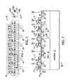
- Figure 2 shows a plan view of a PMOS-gated diode combination device formed with interleaved transistor and diode poly regions in accordance with selected embodiments of the invention
- Figure 3 shows a partial cross-sectional view of the PMOS-gated diode combination device in Figure 2 ;
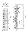
- Figure 4 shows a plan view of an NMOS-gated diode combination device formed with interleaved transistor and diode poly regions and an optional mask defining a drain-side RPO region in accordance with selected embodiments of the invention
- Figure 5 shows a partial cross-sectional view of the NMOS-gated diode combination device in Figure 4 ;
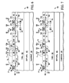
- Figure 6 shows a partial cross-sectional view of an NMOS-gated diode combination device with a first alternate RPO mask defining a drain and source side resistor regions;
- Figure 7 shows a partial cross-sectional view of an NMOS-gated diode combination device with a second alternate RPO mask defaming a drain side resistor region
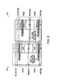
- Figure 8 shows selected layout benefits of interleaving the output buffer and gated diode combination device in accordance with selected embodiments of the present invention.
- Figure 9 shows an example process flow for fabricating a combined output buffer and gated diode in accordance with selected embodiments of the present invention:
- ESD protection device and associated methods of operation and fabrication are described for protecting I/O pad cells of an integrated circuit
- the ESD protection device includes an output buffer transistor and gated diode combination formed compactly in the same layout area by interleaving multi-fingered gate and diode poly layers with body tie regions such that one or more diode body tie regions are isolated from the transistor drain region(s) by the interleaved diode poly layer(s) to form high performance gated diodes.
- the ESD protection circuit uses inherent drain-body diodes of the output buffer transistors to form ESD diodes.
- additional body tie diffusions are formed adjacent to the source diffusions at the output buffer transistors without an isolation region (ST1) between the two diffusion regions, thereby forming butted source-body tie diodes.
- ST1 isolation region
- the body tie regions may be positioned in the substrate using the multi-fingered gate and diode poly layers as an implant or diffusion mask to define a repetitive insertion pattern to distribute the body tie regions uniformly over the entire MOSFET layout.
- selected drain regions in the active areas of the output buffer transistor are shared between the output buffer transistor and the diode, and the number/frequency of inserted diode junctions (body tie regions) depends on the required ESD diode strength versus size of the output buffer transistor, which is typically defined by the drive strength requirement of the output buffer transistor.
- ESD diodes 110, 112, 120 may be implemented with shallow trench isolation (STI) diodes formed between the heavily N-doped (N+) active and heavily P-doped (P+) active diffusion regions. While the ESD diodes 110, 120 may be formed from the drain to body (i.e. N-well or P-well tie) STI diodes inherent to output buffer transistors 114, 122, respectively, such inherent STI diodes may be too resistive to provide robust ESD protection with typical output buffer physical layouts.
- STI shallow trench isolation
- STT diodes 110, 120 are usually formed in separate regions from the I/O cell, requiring significant layout area in order to conduct the majority of the ESD current while minimizing their on-resistance and requiring isolating guard rings between buffers and the STI diodes.
- the formation of output buffers and STI diodes in separate regions also imposes metal routing and device floor-planning limitations, reduces the failure current due to higher dissipated power density on silicon, and impairs the ESD performance (low on-conductance, high turn-on delay) for STI diodes that are inherent to the buffer device. Accordingly, a need exists for an improved ESD protection device and method of operation that overcome the problems in the, art, such as outlined above. Further limitations and disadvantages of conventional processes and technologies will become apparent to one of skill in the art after reviewing the remainder of the present application with reference to the drawings and detailed description contained herein.
- FIG. 2 there is depicted a plan view 200 of a PMOS-gated diode combination device, shown on the right as ESD protection device 270 formed with a gated diode 271 coupled in parallel with PMOS output buffer transistor 272 having a first current electrode coupled to the VDD, a second current electrode coupled to an I/O pad, and a control electrode for receiving a predriver signal PDP from a predriver circuit (not shown).
- ESD protection device 270 formed with a gated diode 271 coupled in parallel with PMOS output buffer transistor 272 having a first current electrode coupled to the VDD, a second current electrode coupled to an I/O pad, and a control electrode for receiving a predriver signal PDP from a predriver circuit (not shown).
- the ESD protection device 270 is fabricated in the active semiconductor layer (enclosed by the dashed line) by forming the PMOS output buffer transistor 272 as a multi-finger MOSFET device that is laid out with alternating source (S) and drain (D) substrate regions separated from one another by a poly gate layer 210 having a plurality of gate poly fingers 201-213.
- the gated diode 271 is formed with a plurality of body tie substrate regions (B) that are positioned next to the drain regions and isolated therefrom by diode poly structures 220, 230, 240, 250, 260 forming diode poly fingers 221, 222, 231, 232, 241, 242, 251, 252, 261, 262 that are arranged in parallel to the gate poly fingers 201-213, thereby forming gated junctions (diodes) between the drain (D) and body (B) regions.
- diode poly structures 220, 230, 240, 250, 260 forming diode poly fingers 221, 222, 231, 232, 241, 242, 251, 252, 261, 262 that are arranged in parallel to the gate poly fingers 201-213, thereby forming gated junctions (diodes) between the drain (D) and body (B) regions.
- body tie substrate regions formed adjacent or butted to the source (S) regions that are positioned laterally from the drain regions and isolated therefrom by transistor poly layers (e.g., 201, 202), thereby forming additional butted source-body tie diodes between the body and drain of the PMOS output buffer transistor 272.
- the multi-finger gated diode 271 and MOSFET output buffer device 272 are formed within the same layout area by defining the mutti-fingered transistor poly layer 210 which is interleaved with a plurality of parallel diode poly structures 220, 230, 240, 250, 260. thereby providing an area efficient output buffer transistor layout.
- the depicted ESD protection device 270 includes thirteen parallel connected transistors and ten parallel connected lateral diodes, it will be appreciated that the number or frequency of inserted diode poly fingers (and associated body tie regions) relative to the number of transistor poly fingers can be adjusted, depending on the desired ESD diode strength versus size of the MOSFET.
- the output buffer transistor is shown as being implemented with a plurality of relatively small parallel connected transistors in a multi-finger gate poly structure 210 which is interleaved with five separate multi-finger diode poly structures 220, 230, 240, 250, 260.
- the multi-finger diode poly structures can be formed as a single multi-finger diode poly structure so long as there are no different voltage requirements for the different diode poly structures.
- the multi-finger gate poly structure 210 may be implemented with a plurality of separate multi-finger gate poly structures which would e.g.
- PMOS output buffer transistor 272 is implemented as an integrated circuit formed with an n-well 302 and a p-type substrate 301. and includes a plurality of parallel-connected transistors T1, T2, T3, etc. having a corresponding plurality of gate poly fingers 203-205.
- the gated diode 271 is also formed over the n-well 302 with a plurality of parallel-connected diodes (e.g., 331, 332) having a corresponding plurality of diode poly fingers 231, 232.
- the gate and diode poly fingers are positioned to interleave with one another in an alternating pattern of parallel fingers with diode poly fingers laterally adjacent to gate poly Fingers.
- the diode poly fingers may have a smaller width dimension than the gate poly fingers since the diode poly fingers do not have the same electrical performance requirements, but any desired feature width can be used for the different poly fingers.
- Each gate poly finger defines a transistor (e.g., T1, T2. T3) having a first current electrode (e.g., P+ source region 310 and its associated silicide layer 318) coupled to VDD, a second current electrode (e.g., P+ drain region 309 and its associated silicide layer 317) coupled to an I/O pad, and a gate electrode (e.g., gate finger 203 and its associated silicide layer 316) coupled to receive predriver signal PD.P.
- each diode poly finger e.g., 222, 231, 232
- diode poly finger 231 defines a first diode D2 3.1 having a first current electrode (e.g., P+ drain region 312 and its associated silicide layer 319) coupled to I/O and a second current electrode (e.g., N+ body region 307 and its associated silicide layer 320) coupled to VDD, thereby forming a P-N junction between the p-type region (e.g., P+ drain region 312) and the n-type region (e.g., the N-well 302).
- a first current electrode e.g., P+ drain region 312 and its associated silicide layer 319
- a second current electrode e.g., N+ body region 307 and its associated silicide layer 320
- An additional parallel connected diode may be formed from the same n-type region (e.g., the N-well 302) by forming a second p-type region (e.g., P+ drain region 313) to be separated from the n-type region 307 by another diode poly finger 232, thereby defining a diode D3 332 having a first current electrode (e.g., P+ drain region 313 and its associated silicide layer 321) coupled to I/O and a second current electrode (e.g., N+ body region 307 and its associated silicide layer 320) coupled to VDD.
- a first current electrode e.g., P+ drain region 313 and its associated silicide layer 321
- a second current electrode e.g., N+ body region 307 and its associated silicide layer 320
- the diode poly fingers are shown as floating elements that are not connected to any electrode, this is not necessarily the case since the diode poly fingers could be connected to a reference voltage (e.g., VDD) or any other signal line if desired to control or alter the electrical performance of the associated diode.
- VDD reference voltage
- the p-substrate 301 is coupled to VSS_BULK 105 of Figure 1 .
- the depicted PMOS-gated diode combination device 300 includes multiple body ties that connect the N-well 302 to VDD, such as the N+ diffusion regions 306, 308 that provide body ties for transistors T1-T3 and are butted to the P+ source regions 310-311, 314 and coupled to VDD by silicide layers 318, 322. These N+ diffusion regions 306, 308 define diodes (not shown) that are inherent to each of the transistors T1-T3.
- These diodes are formed by P-N junctions between the N+ body tie diffusion regions (e.g., 306) and N-well 302, on the one hand, and the P+ diffusion regions (e.g., 309, 312) that function as drains for each of the butted source-body tie output buffer transistors T 1, T2, respectively, on the other hand.
- selected embodiments do not include the body diffusion regions 30G, 308 between source regions, in which case a single source region can be shared by the transistors (e.g., T1 and T2), thereby providing a smaller layout.
- Figure 3 also shows that lateral gated diodes 331, 332 are defined with reference to the diode poly fingers (e.g., 231, 232) and illustrated with dashed lines, These gated diodes 331, 332 are formed by P-N junctions between the N+ body regions (e.g., 307) and N-well 302, on the one hand, and the P+ diffusion regions 312, 313 that function as drains for the adjacent output buffer transistors T2, T3, respectively, on the other hand.
- N+ body regions e.g., 307
- the P-N junctions for the gate diodes are formed by fabricating drain and body tie "finger" regions having an opposite conductivity types and isolated from one another by diode poly fingers using a repetitive insertion pattern to distribute them uniformly over the entire MOSFET layout so that the drain regions are shared between the transistor and the diode elements.
- the overall drain-to-body lateral diode inherent to such a combination device forms a strong ESD diode.
- diode 331 provides an ESD current path from the I/O connection (via P+ drain region 312) to VDD (via N+ body region 307), wherein the current flows through silicide layer 319 to P+ drain region 312, crosses the P-N junction formed by P+ drain region 312 and N-well 302, continues to flow in the N-well to the N+ body tie diffusion 307, and then flows through silicide layer 320 to VDD. With this discharge path, the total diode resistance is lower than would be required to penetrate deeper around an STI region.
- selected embodiments of the present invention may also be implemented with NMOS output buffer transistors by forming the transistors in a p-type substrate or well region, reversing the conductivity type of the diffusion regions, and replacing VDD by VSS.
- FIG. 4 shows a plan view 400 of an NMOS-gated diode combination device, shown on the right as ESD protection device 450 formed with a gated diode 451 coupled in parallel with NMOS output buffer transistor 452 having a first current electrode coupled to an I/O pad, a second current electrode coupled to the VSS, and a control electrode for receiving a predriver signal PD.N from a predriver circuit (not shown).
- the ESD protection device 450 is fabricated by forming interleaved transistor gate poly fingers 401-407 and diode poly fingers 421, 422, 431,432,441,442.
- the niulti-finger NMOSFET device 452 is laid out with alternating source (S) and drain (D) substrate regions separated from one another by a poly gate layer 410 having a plurality of gate poly fingers 401-407.
- the gated diode 451 is formed with a plurality of body tie substrate regions (B) that are positioned next to the drain regions and isolated therefrom by diode poly layers 420, 430, 440, thereby forming gated junctions (diodes) between the drain (D) and body (B) regions.
- the ESD protection device 450 may be fabricated to include a drain-side resistor element 453 between the NMOS output buffer transistor 452 and the I/O pad.
- the plan view 400 of an NMOS-gated diode combination device shows that optional mask elements 411-417 are provided to define one or more drain-side resistor-protect-oxide (RPO) regions in the substrate which are used to prevent the formation of silicide in these areas, thereby increasing their Ohmic resistance.
- RPO drain-side resistor-protect-oxide
- the NMOS-gated diode combination device 500 includes an NMOS output buffer transistor 452 and gated diode 451 formed in a p-well 503, which in turn is located above a deep n-well 502 formed in the p-type substrate 501.
- the p-substrate 501 is coupled to VSS_BULK 105 of Figure 1 .
- the p-well 503 may be formed as an isolated p-well (IPW) that is used with I/O designs to provide noise isolation between the VSS and VSS_BULK buses.
- IPW isolated p-well
- the p-well 503 may be fully isolated from the P-substmte 501 by providing an n-well ring around the buffer to form an IPW tub.
- the NMOS output buffer transistor 452 includes a plurality of parallel-connected transistors (e.g., T1, T2,) having a corresponding plurality of gate poly fingers 402-403 formed over the p-well 503.
- the gated diode 451 is also formed over the p-well 503 with a plurality of parallel-connected diodes (e.g., 521, 522) having a corresponding plurality of diode poly fingers 431, 432. As depicted, the gate and diode poly fingers are positioned to interleave with one another in an alternating pattern of parallel fingers including diode poly fingers laterally adjacent to gate poly fingers.
- a plurality of parallel-connected diodes e.g., 521, 522
- the gate and diode poly fingers are positioned to interleave with one another in an alternating pattern of parallel fingers including diode poly fingers laterally adjacent to gate poly fingers.
- each gate poly finger defines a transistor (e.g., T1) having a first current electrode (e.g., N+ drain region 508 and its associated silicide layer 514) coupled to the I/O pad, a second current electrode (e.g., N+ source region 509 and its associated silicide layer 516) coupled to VSS, and a gate electrode (e.g., gate finger 402 and its associated silicide layer 513) coupled to receive predriver signal PD.N.
- a transistor e.g., T1 having a first current electrode (e.g., N+ drain region 508 and its associated silicide layer 514) coupled to the I/O pad, a second current electrode (e.g., N+ source region 509 and its associated silicide layer 516) coupled to VSS, and a gate electrode (e.g., gate finger 402 and its associated silicide layer 513) coupled to receive predriver signal PD.N.
- each diode poly finger defines a diode (e.g., D2) having a first current electrode (e.g., N+ drain region 510 and its associated silicide layer 518) coupled to I/O and a second current electrode (e.g., P+ body region 507 and its associated silicide layer 519) coupled to VSS, thereby defining a lateral diode from the P-N junctions between the p-type region (e.g., p-well 503) and the n-type region (e.g., the N+ drain region 510).
- a first current electrode e.g., N+ drain region 510 and its associated silicide layer 518
- a second current electrode e.g., P+ body region 507 and its associated silicide layer 519
- the diode poly fingers are shown as floating elements, but they may be connected to a reference voltage (e.g., VSS) or any other signal line if desired to control or alter the electrical performance of the associated diode.
- VSS reference voltage
- the source and body terminals of NMOS output buffer transistor 452 may be electrically isolated from each other.
- the P+ body regions (e.g., 507) and its associated silicide layers (e.g. 519) may not be coupled to VSS, as shown in Figure 5 , but to another supply rail, e.g. VSS_BULK, to provide an ESD diode between I/O and VSS_BULK.
- the NMOS-gated diode combination device 500 may include drain side resistor elements formed in the transistor drain regions for purposes of controlling the current flow through the NMOS output buffer transistor 452 to provide a more uniform turn-on ("snapback") of the plurality of bipolar junction transistor fingers inherent to the mutti-finger NMOS output buffer transistor 452 during an ESD event.
- a bipolar junction transistor finger inherent to NMOS T2 comprising gate finger 403 is formed by N+ region 509 ("Emitter"), p-well 503 ("Base”), and N+ region 510 ("Collector"). While resistor elements are not necessarily required, they can be inserted using any of a number of different fabrication techniques.
- Figure 4 shows that mask elements 411-417 may be formed over the drain region prior to silicide formation, thereby defining one or more drain-side resistor-prolect-oxide (RPO) regions in the substrate below the mask elements 411-417.
- RPO drain-side resistor-prolect-oxide
- Figure 5 shows a plurality of separately patterned mask elements 412-414 formed with patterned oxide layers on the substrate to cover a portion of the N+ drain regions 508, 510, 511 so as to prevent substrate silicide layers 514-520 from being formed where the patterned mask elements 412-414 are located.
- a first resistive element is formed in the unsilicided portion of the N+ drain region 508 between the silicide layer 514 connected to the I/O terminal and the silicide layer 515 in the N+ drain region 508 that is adjacent to the gate electrode 402.
- a second resistive element is formed in the unsilicided portion of the N+ drain region 510 between the silicide layer 518 connected to the I/O terminal and the silicide layer 517 in the N+ drain region 510 that is adjacent to the gate electrode 403.
- silicide layers e.g., 514 and 515.
- an adjacent silicide layer e.g., 515
- an I/O terminal silicide layer e.g., 514
- the width of the unsilicided portions of the N+ drain regions may be adjusted and controlled to increase or decrease the values of the inserted drain side resistor elements, thereby decreasing or increasing the current flow through the NMOS output buffer transistor 452.
- the drain side resistor elements are effectively removed by not using mask elements 411-417 in the fabrication process.
- the length of mask elements 411-417 can be extended over the transistor gates towards the source regions to further increase the resistance values associated with each transistor.
- a drain ballasted MOSFET device where the RPO mask element overlaps the drain and gate elements cannot be treated simply as a combination of a MOSFET transistor and a series RPO resistor.
- Dedicated design kit support with regards to layout versus schematic (LVS) checks, layout design rule checks (DRC), and compact modeling to describe the electrical behavior of such a device would be required.
- FIG. 6 shows a partial cross-sectional view of an NMOS-gated diode combination device 600 with a plurality of separately patterned mask elements 610-612 formed in accordance with an alternate RPO mask defining drain and source side resistor regions.
- the alternate RPO mask elements 610-612 are formed to define resistive elements in unsilicided portions of the N+ source and drain regions 608 of each transistor (e.g., T1).
- the patterned mask elements (e.g., 610) are formed prior to silicidation in order to cover part of the N+ drain region, all of the gate layer 606, and part of the N+ source region 608, but as indicated by the dashed lines, the mask elements 610-612 may be removed prior to formation of the electrode contact layers so that the I/O, predriver and VSS lines can be connected to the NMOS-gated diode combination device, with or without contact silicide layers being formed.
- This use of the patterned mask elements 610-612 at this stage of device fabrication prevents substrate silicide layers 614 from being formed where the patterned mask elements 610-612 are located.
- a first series-connected resistive element is formed in the unsilicided portion of the N+ drain region 608 between the silicide layer 614 connected to the I/O terminal and the gate electrode 606
- a second series-connected resistive element is formed in the unsilicided gate electrode 606
- a third series-connected resistive element is formed in the unsilicided portion of the N+ source region 608 between the silicide layer 614 connected to the VSS terminal and the gate electrode 606.
- the placement of the patterned mask elements 610-612 may be controlled so that the lateral gated diodes 621, 622 are not affected.
- Figure 7 shows a partial cross-sectional view of an NMOS-gated diode combination device 700 with a plurality of separately patterned mask elements 701-703 formed in accordance with an alternate RPO mask defining drain side resistor regions.
- the alternate RPO mask elements 701-703 are formed over the p-well 603 (and underlying n-well 602 and p-substrate 601) and patterned gate electrodes 606 with sidewall spacers 609 to cover part of the implanted N+ drain regions 608 and part of the gate electrode 606 to define resistive elements in unsilicided portions of the N+ drain regions 608 and gate electrode 606 of each transistor (e.g., T1).
- the patterned mask elements e.g., 701 are formed prior to silicidation in order to cover part of the N+ drain region and part of the gate layer 606.
- the mask elements 701-703 may be removed prior to formation of the electrode contact layers so that the I/O, predriver and VSS lines can be connected to the NMOS-gated diode combination device, with or without contact silicide layers being formed.
- This use of the patterned mask elements 701-703 at this stage of device fabrication prevents the gate silicide layers 704 and substrate silicide layers 705 from being formed where the patterned mask elements 701-703 are located, thereby forming a first series-connected resistive element in the unsilicided portion of the N+ drain region 608 between the silicide layer 705 connected to the I/O terminal and the gate electrode 606.
- a second series-connected resistive element is formed in the gate electrode 606 where the gate silicide layer 704 is not located.
- the placement of the patterned mask elements 701-703 may be controlled so that the lateral gated diodes 721, 722 are not affected.
- drain coverage dimension X D The extent of the drain coverage by the patterned mask elements is defined by a drain coverage dimension X D
- source coverage dimension X S The extent of the source coverage is defined by a source coverage dimension X S .
- the minimum coverage of a source or drain region will be limited by the minimum design rule for any given fabrication process, but should be controlled to allow the subsequently formed silicide layers to provide good Ohmic contact to the substrate.
- the ESD protection device uses a combined output buffer and gated diode integrated circuit structure having a multi-finger MOSFET device and a multi-finger diode device formed in a shared layout area with alternating source and drain regions separated by gate poly fingers and with body tie regions inserted next to drain regions and isolated therefrom by diode poly fingers to form gated diodes between the drain and body region.
- the disclosed ESD protection device provides one or more advantages by providing ESD protection circuits with reduced layout area requirements since the output buffer and ESD diode can be formed in a shared layout area instead of in separate areas requiring separate guard ring structures.
- Figure 8 shows an integrated circuit layout 810 for implementing the ESD protection circuit of Figure 1 with conventional output buffer and STI diode structures.
- the component transistor elements e.g., M1.
- PMOS, NMOS e.g., NMOS
- diode elements e.g., A1, A2, B, C, D
- PAD landings e.g., PAD landings, VSS_BULK 812, VSS 813, TRIGGER 814, VDD 815, and BOOST 816.
- the PMOS output buffer transistors are conventionally formed in separate layout regions from the ESD diodes (A1)
- the NMOS output buffer transistors (NMOS) are conventionally formed in separate regions from the ESD diodes (B).
- PMOS PMOS output buffer transistors
- NMOS NMOS output buffer transistors
- the integrated circuit layout 820 for the interleaved output buffer and gated diode combination device where the PMOS output buffer transistors (PMOS) and associated ESD diodes (A1) are formed in the same layout area.
- NMOS NMOS output buffer transistors
- B ESD diodes
- the clamp device (M 1) and diode elements are each formed in separate layout areas and connected to their respective voltage, signal and/or PAD landings (e.g., PAD landings, VSS_BULK 822, VSS 823, TRIGGER 824, VDD 825, and BOOST 826).
- the PMOS output buffers and ESD diodes A1 are formed in a first shared layout area to be connected to the PAD landing and VSS 823, while the NMOS output buffers and ESD diodes B are formed in a second shared layout area so as to be connected to the PAD landing and VDD 825.
- This approach also eliminates the need for an additional metal layer to jumper the guard rings to connect the buffers to the 1/0 pad, or alternatively eliminates the requirement of two additional PAD landings for connecting the buffers.
- ESD protection device there are also performance benefits that may result from the disclosed ESD protection device, such as improved ESD performance by reducing the effective resistance of the gated ESD diodes as compared to STI diodes. Parasitic metal resistance may also be reduced since the drain metal fingers that are shared between the MOSFET and the gated diode can be made wider compared to standalone diodes.
- the disclosed ESD protection device also provides a higher failure current as compared to standalone ESD diodes since the diode fingers are spread out over a larger area, thereby reducing the dissipated power density and increasing the thermal failure point due to self-heating during ESD.
- the disclosed ESD protection device with gated diodes provides improved performance (high on-conductance, low turn-on delay) as compared to conventional STI diodes that are inherent to the buffer device (drain-body junction), and has reduced susceptibility to latchup compared to a simple perimeter body tie resulting from the additional body tie regions in the disclosed ESD protection device which improve the overall body strapping of the buffer.
- an improved ESD protection device is provided by interleaving a multi-fingered output buffer transistor with a multi-fingered gated diode device with diode poly fingers that isolate drain regions from body tie regions in the substrate.
- Figure 9 shows an example process flow 900 for fabricating a combined output buffer and gated diode in accordance with selected embodiments of the present invention. Though selected embodiments of the fabrication sequence are illustrated in Figure 9 , it will be appreciated that the sequence of illustrated steps may be modified, reduced or augmented in keeping with the disclosure of the present invention. For example, one or more of the steps may optionally be included or excluded. Thus, it will be appreciated that the methodology of the present invention may be thought of as performing the identified sequence of steps in the order depicted in Figure 9 , though the steps may also be performed in parallel, in a different order, or as independent operations that are combined.
- the methodology begins at step 901 by providing a substrate in which n-wells and/or p-wells are formed, depending on the type of output buffer being fabricated.
- the semiconductor substrate may be formed of a material having first conductivity type impurities, such as a p-type substrate layer 301, at a predetermined P-doping level (e.g., approximately 1E15 cm -3 ), though any desired dopant type and/or concentration may be used.
- the substrate 301 may be formed as a bulk semiconductor substrate, a semiconductor-on-insulator (SOI) type substrate in which one or more additional semiconductor layers and/or well regions are formed using epitaxial semiconductor growth and/or selective doping techniques, or any semiconductor material including, for example, Si, SiC, SiGe, SiGeC, Ge, GaAs, InAs, InP, as well as other III/V or II/VI compound semiconductors or any combination thereof, alone or in combination with an epitaxial layer (e.g., p-type epi layer).
- SOI semiconductor-on-insulator
- the invention is not limited to any specific substrate type.
- an n-well region 302 may be formed for at least the active PMOS device area.
- the n-well 302 may be formed of a material having a second conductivity type impurities by using a mask to selectively diffuse or implant n-type impurities into the substrate 301 to a predetermined implant energy and dopant concentration so as to be located at a sufficient depth that will contain the subsequently formed PMOS transistor and gated diode.
- a gate dielectric is formed over the substrate, followed by formation of a poly layer over the gate dielectric layer (step 903).
- the gate dielectric layer 303 may be formed by depositing or growing an insulator or dielectric (e.g., silicon dioxide, oxynitride, metal-oxide, nitride, etc.) over the semiconductor substrate using chemical vapor deposition (CVD), plasma-enhanced chemical vapor deposition (PECVD), physical vapor deposition (PVD), atomic layer deposition (ALD), thermal oxidation, or any combination(s) of the above.
- CVD chemical vapor deposition
- PECVD plasma-enhanced chemical vapor deposition
- PVD physical vapor deposition
- ALD atomic layer deposition
- thermal oxidation or any combination(s) of the above.
- a conductive layer 304 is formed or deposited over the gate dielectric layer using CVD, PECVD, PVD, ALD, or any combination(s) thereof to a predetermined thickness, though other fabrication methods may be used.
- the conductive layer 304 may be formed with polysilicon or with a doped or undoped amorphous silicon or silicon-germanium layer, though other materials may be used.
- the conductive layer 304 may be formed with metal-based layers by depositing one or more metal layers or other conductive materials, alone or in combination with a polysilicon layer, along with more exotic processing, like selective deposition/epitaxy or direct beam writing.
- the gate dielectric and poly layers are patterned and selectively etched to define the poly gate layer 210 having a plurality of gate poly fingers 201-213, and separate but interleaved diode poly structures 220, 230, 240, 250, 260 having a plurality of diode poly fingers 221-222, 231-232,241-242,251-252,261-262.
- any desired pattern and etching processes may be used to form the patterned poly gate and diode fingers over the semiconductor substrate, including application and patterning of photoresist on the polysilicon layer 304, though multi-layer masking techniques may also be used.
- RPO mask elements may be formed in the same substrate regions as the gated diode poly layers to effectively form a lateral diode junction between implanted drain and body finger regions by avoiding silicidation of the junction of the intended diode.
- a plurality of separate implant mask and implantation processes are used (step 905) to form the contact region(s) 3115-314, including N+ regions 305-308 and P+ regions 309-314, either before or after forming sidewall spacers 315 on the sidewalls of the patterned poly gate and diode fingers.
- lightly doped source/drain regions may be implanted around the patterned poly gate and diode fingers using one or more mask and implantation steps, followed by formation of sidewall spacers 315 and then implantation of the N+ regions 305-308 and P+ regions 309-314.
- a dielectric layer e.g., silicon oxide or silicon nitride
- the dielectric layer may then be selectively etched using one or more anisotropic etch processes to form sidewall spacers 315, including a dry etching process (such as reactive-ion etching, ion beam etching, plasma etching, laser etching), a wet etching process (wherein a chemical etchant is employed) or any combination thereof.
- the N+ regions 305, 307 may be formed adjacent to the diode poly fingers by using an implant mask (not shown) to selectively implant n-type impurities into the n-well region 302 to a predetermined depth using a predetermined implant energy and dopant concentration to form body regions for the gate diode.
- the N+ diffusion regions 306, 308 may be formed using an implant mask (not shown) to selectively implant n-type impurities adjacent to the intended source regions in the n-well region 302 to form body regions for the diodes (not shown) inherent to each of the transistors T1-T3.
- the P+ regions 309-314 may be formed by using an implant mask (not shown) to selectively implant p-type impurities into the n-well region 302 to a predetermined depth using a predetermined implant energy and dopant concentration to form source and drain regions for the PMOS transistor.
- one or more silicide mask layers may be selectively formed over the substrate to define resistor elements in the ESD protection device.
- the silicide mask formation step is performed in some embodiments, but provides a way to define resistive elements in unsilicided portions of the substrate and/or gate as desired.
- the patterned mask elements 4.12-414 may be formed by depositing a layer of nitride or oxide that is selectively patterned and etched to cover predetermined portions of the N+ drain regions 508, 510, 511 so as to prevent substrate silicide layers 514-520 from being formed where the patterned mask elements 412-414 are located.
- silicide layers may be formed on the appropriate source/drain regions and patterned poly gate and diode fingers.
- the selective formation of silicide is formed by depositing one or more metal layers over the exposed semiconductor substrate and patterned poly gate and diode fingers, such as by using a blanket or sputter deposition process to form a metal layer that will be used to form silicide on the exposed gate and substrate regions, such as the exposed source/drain and body regions.
- the reaction of the first metal layer and the underlying semiconductor material to form the silicide regions 316-322 is promoted by performing an initial rapid thermal anneal step, followed by a wet clean step to remove the unreacted metal from the dielectric areas (e.g., spacers and trench regions), and then followed by an optional second anneal step.
- the anneal can be rapid thermal processing, furnace anneal, spike anneal or laser anneal, for example.
- the timing and temperature of the anneal process is controlled to react metal in first metal layer with the underlying polysilicon or other semiconductor material in source/drain regions, but not with the sidewall spacer material 315.
- any unreacted portion of the first metal layer is selectively removed with an appropriate metal etch, such as a Piranha wet clean process.
- one or more metallization layer(s) are formed to define terminals for the ESD protection device.
- one or more backend processing may be used to form electrode contacts to the N+ and P+ 305-314 and silicide regions 316-322 by depositing one or more dielectric or masking layers which are then patterned and selectively etched to define openings over the contact and gate poly regions.
- one or more conductive layers are deposited, masked and selectively etched to form I/O contacts to the transistor drain regions 309, 312, 313.
- VDD contacts are made to the diode body region 307, and also to the body diffusion regions 306, 308 and source regions 310, 311, 314, which are abutted to and shorted with silicide to their respective body regions.
- predriver signal PD.P contacts are made to the PMOS transistor gates 203, 204, 205.
- the fabrication process ends at step 909.
- separate standalone ESD diodes may be placed in parallel with the lateral inherent gated diodes (e.g., 331, 332 in Figure 3 ).
- butted source-body tie diodes may be formed by including the body tie regions between the source regions as shown in Figures 2-3 .
- the lateral inherent gated diodes may, in selected embodiments, serve as the primary or only ESD diodes, conducting a majority of the ESD current.
- the boost buss 101 shown in Figure 1 may be shorted to the VDD bus 102, thereby eliminating the need for A2 diode 112 in Figure 1 and the A2 diodes in Figure 8 .
- the lateral parasitic gated diodes may be used for either or both of the pull-up transistor(s) 114 and the pull-down output transistor 122.
- the resulting ESD protection devices provide significantly higher failure current and significantly higher conductivity as compared to, for example, STI bounded diodes with an equal P-N junction perimeter, due primarily to the fact that the ESD current need not flow under any STI, but may flow much less impeded, along the silicon surface.
- the lateral gated diodes may reduce capacitive loading on the I/O pad because there are no added diffusion regions tied to the pad, as would be the case for separately placed STI diodes.
- an integrated circuit electrostatic discharge (ESD) protection device for connecting a power supply conductor (e.g., VDD or VSS) and conductive pad across a parallel connected output buffer transistor and gated diode.
- the output buffer transistor is formed in a first layout area with a PMOSFET or NMOSFET gate electrode that is coupled to receive a control signal and that is formed over a substrate with one or more conductive gate fingers. Each gate finger separates a source and drain region of a first conductivity type formed in the substrate.
- the output buffer transistor is formed as a partially silicided drain region defining a drain-side resistive element.
- the gated diode is formed in the same first layout area as the output buffer transistor with one or more conductive diode fingers and a corresponding one or more body tie regions of a second conductivity type formed in the substrate. As formed, each body tie region is separated or isolated from a corresponding drain region from the output buffer transistor by a conductive diode finger.
- the output buffer transistor is implemented as a plurality of parallel connected butted source-body tie output buffer transistors
- the plurality of conductive gate fingers may extend perpendicularly from a single conductive gate spine
- the gated diode may be implemented as a plurality of parallel connected diodes defined by the plurality of conductive diode fingers which are interleaved with and parallel to the plurality of conductive gate fingers, wherein each of the plurality of parallel connected diodes comprises a gated diode inherent to the output buffer transistor for conducting ESD current.
- the gated diode may be formed by a P-N junction between a well of a first conductivity type (e.g., n-type) and a diffusion region of a second conductivity type (e.g., p-type) that functions as a drain of the output buffer transistor.
- a first conductivity type e.g., n-type
- a second conductivity type e.g., p-type
- the 1C device includes a first conductor (e.g., pad conductor), a second conductor (e.g., power supply conductor), a third conductor (e.g., a power supply conductor), and a MOSFET transistor that is formed in a substrate region of a first conductivity type.
- the transistor includes a gate electrode and source and drain regions of a second conductivity type formed in the substrate region, where the drain region is coupled to the first conductor, the source region is coupled to the third conductor, the substrate region is coupled to the second conductor, and the gate electrode is formed over the substrate region with a conductive gate layer which separates the source and drain regions.
- the 1C device also includes a diode formed in the same substrate region as the MOSFET transistor and coupled between the first and second conductors.
- the diode is formed from a body tie region of the first conductivity type formed in the substrate and the MOSFET transistor drain region of the second conductivity type, where a diode finger layer is formed over the substrate region in parallel with the gate layer to separate the body tie region and MOSFET transistor drain region.
- the conductive gate layer is formed as a plurality of conductive gate fingers extending perpendicularly from a single conductive gate spine, and the diode layer is formed as a plurality of conductive diode fingers which are interleaved with and parallel to the plurality of conductive gate fingers.
- the diode layer is formed from a dielectric layer, a polysilicon layer, one or more metal layers, or a resistor-protect-oxide (RPO) layer.
- a metal-based contact layer may be formed on the MOSFET transistor drain region that is shared between the MOSFET transistor and diode and that is connected to an input and/or output pad.
- a semiconductor device and process for forming same In the disclosed process, a semiconductor substrate is provided, a first well region of a first conductivity type is formed in the semiconductor substrate, and a patterned gate electrode finger layer and patterned diode finger layer are formed over at least pan of the first well region. In addition, source and drain regions of a second opposite conductivity type are formed in the first well region and adjacent to the patterned gate electrode finger, thereby defining an output buffer transistor. There is also formed a body tie region of the first conductivity type in the first well region and adjacent to the patterned diode finger layer, thereby defining a gated diode between the body tie region and the drain region such that the gated diode is coupled in parallel with the output buffer transistor.
- one or more conductive layers are formed to connect the body tie region to a power supply conductor and to connect the drain region to a conductive pad.
- the formation of conductive layers may include forming a silicide layer to partially cover the drain region, thereby defining a drain-side resistive element.
- the described exemplary embodiments disclosed herein are directed to an ESD protection device and associated method of manufacture in which an output buffer transistor with a multi-fingered gated diode device is interleaved with diode poly fingers that isolate drain regions from body tie regions in the substrate
- the present invention is not necessarily limited to the example embodiments which illustrate inventive aspects of the present invention that are applicable to a wide variety of integrated ESD protection circuits with combined output buffer and gated diode.
- the particular embodiments disclosed above are illustrative only and should not be taken as limitations upon the present invention, as the invention may be modified and practiced in different but equivalent manners apparent to those skilled in the art having the benefit of the teachings herein.
Landscapes
- Semiconductor Integrated Circuits (AREA)
- Metal-Oxide And Bipolar Metal-Oxide Semiconductor Integrated Circuits (AREA)
Abstract
Description
- The present invention is directed in general to integrated circuit electrostatic discharge (ESD) protection devices and methods for operating same. In one aspect, the present invention relates to an ESD protection circuit that uses output transistors and diodes as ESD protection devices.
- An integrated circuit (IC) may be subject to an ESD event in the manufacturing process. during assembly and testing, or in the system application. Some onchip ESD protection networks use an active MOSFET (metal oxide semiconductor field-effect transistor) rail clamp protection scheme with large ESD diodes between the input/output (1/O) pads and the power supply rails.
-
Figure 1 illustrates in schematic diagram form a conventionalESD protection circuit 100 for protecting an 1/0pad 116. TheESD protection circuit 100 is connected to aboost bus 101, a first power supply VDD 102, atrigger bus 103, a second power supply VSS 104, and a third power supply VSS_BULK 105. In theESD protection circuit 100, arail clamp device 117 has current electrodes coupled between the VDD 102 and VSS 104. Though shown as an NMOS MOSFET transistor, therail clamp device 117 may be of a different type, for example, a PMOS transistor, a BJT (bipolar junction transistor), an SCAR (silicon-controlled rectifier), or a GGMOS (grounded gate MOS) transistor. TheESD protection circuit 100 also includes atrigger circuit 118 that is coupled between theboost bus 101 and VSS 104 for providing atrigger signal 119 to the gate of the railclamp transistor device 117. Other clamp trigger signals can also be provided on thetrigger buss 103. As depicted, afirst diode 110 is coupled betweenVDD 102 and the I/O pad 116, asecond diode 112 is coupled between theboost bus 101 and the I/O pad 116, and athird diode 120 is coupled between the I/O pad 116 and the VSS 104. There are also first andsecond diodes ESD protection circuit 100 also includes a PMOS (P-type metal oxide semiconductor)output buffer transistor 114 and an NMOS (N-type metal oxide semiconductor)output buffer transistor 122 coupled to drive an internally generated signal on an I/O pad 116. The gates ofoutput buffer transistors - As will be appreciated,
ESD diodes ESD diode 110 provides a high-current ESD path from the I/O pad 116 to VDD in case of a positive ESD event on the I/O pad 116, andESD diode 120 provides a high-current ESD path from VSS to I/O pad 116 in case of a negative ESD event on the I/O pad 116. During an ESD event that requires shunting a high ESD current from VDD to the VSS by rail clamp transistor device 117 (e.g., a positive ESD zap on I/O pad 116 with respect to another I/O pad), thetrigger circuit 118 provides the voltage fromboost bus 101 to the gate of railclamp transistor device 117. ESDdiode 112 provides a separate current path from the I/O pad 116 via theboost bus 101 topower trigger circuit 118. Since very little current is required to powertrigger circuit 118, the voltage drop acrossESD diode 112 during an ESD event is much smaller than the voltage drop across diode I 10. In this manner, theboost bus 101 supplies a voltage that is higher than theVDD voltage 102 through thetrigger circuit 118 to the gate of railclamp transistor device 117 during an ESD event, thereby providing increased conductivity of the rail clamp device. Theboost bus 101 can be relatively narrow due to the very little current it needs to conduct. - The present invention may be understood, and its numerous objects, features and advantages obtained, when the following detailed description is considered in conjunction with the following drawings, in which:
-
Figure 1 illustrates a simplified circuit schematic diagram of a conventional ESD protection circuit; -
Figure 2 shows a plan view of a PMOS-gated diode combination device formed with interleaved transistor and diode poly regions in accordance with selected embodiments of the invention; -
Figure 3 shows a partial cross-sectional view of the PMOS-gated diode combination device inFigure 2 ; -
Figure 4 shows a plan view of an NMOS-gated diode combination device formed with interleaved transistor and diode poly regions and an optional mask defining a drain-side RPO region in accordance with selected embodiments of the invention; -
Figure 5 shows a partial cross-sectional view of the NMOS-gated diode combination device inFigure 4 ; -
Figure 6 shows a partial cross-sectional view of an NMOS-gated diode combination device with a first alternate RPO mask defining a drain and source side resistor regions; -
Figure 7 shows a partial cross-sectional view of an NMOS-gated diode combination device with a second alternate RPO mask defaming a drain side resistor region; -
Figure 8 shows selected layout benefits of interleaving the output buffer and gated diode combination device in accordance with selected embodiments of the present invention; and -
Figure 9 shows an example process flow for fabricating a combined output buffer and gated diode in accordance with selected embodiments of the present invention: - An electrostatic discharge (ESD) protection device and associated methods of operation and fabrication are described for protecting I/O pad cells of an integrated circuit, where the ESD protection device includes an output buffer transistor and gated diode combination formed compactly in the same layout area by interleaving multi-fingered gate and diode poly layers with body tie regions such that one or more diode body tie regions are isolated from the transistor drain region(s) by the interleaved diode poly layer(s) to form high performance gated diodes. In selected embodiments, the ESD protection circuit uses inherent drain-body diodes of the output buffer transistors to form ESD diodes. In other embodiments, additional body tie diffusions are formed adjacent to the source diffusions at the output buffer transistors without an isolation region (ST1) between the two diffusion regions, thereby forming butted source-body tie diodes. By using inherent drain-body diodes of output buffer transistors with gated diodes as the dominant ESD diodes, higher performance ESD diodes are formed with reduced layout area requirements as compared to separately placed STI diodes. As disclosed herein, the body tie regions may be positioned in the substrate using the multi-fingered gate and diode poly layers as an implant or diffusion mask to define a repetitive insertion pattern to distribute the body tie regions uniformly over the entire MOSFET layout. In this way, selected drain regions in the active areas of the output buffer transistor are shared between the output buffer transistor and the diode, and the number/frequency of inserted diode junctions (body tie regions) depends on the required ESD diode strength versus size of the output buffer transistor, which is typically defined by the drive strength requirement of the output buffer transistor.
- Various illustrative embodiments of the present invention will now be described in detail with reference to the accompanying figures. While various details are set forth in the following description, it will be appreciated that the present invention may be practiced without these specific details, and that numerous implementation-specific decisions may be made to the invention described herein to achieve the device designer's specific goals, such as compliance with process technology or design-related constraints, which will vary from one implementation to another. While such a development effort might be complex and time-consuming, it would nevertheless be a routine undertaking for those of ordinary skill in the art having the benefit of this disclosure. For example, selected aspects are depicted with reference to simplified cross sectional drawings of a semiconductor device without including every device feature or geometry in order to avoid limiting or obscuring the present invention. Such descriptions and representations are used by those skilled in the art to describe and convey the substance of their work to others skilled in the art. In addition, although specific example materials are described herein, those skilled in the art will recognize that other materials with similar properties can be substituted without loss of function. It is also noted that, throughout this detailed description, certain materials will be formed and removed to fabricate the semiconductor structure. Where the specific procedures for forming or removing such materials are not detailed below, conventional techniques to one skilled in the art for growing, depositing, removing or otherwise forming such layers at appropriate thicknesses shall be intended. Such details are well known and not considered necessary to teach one skilled in the an of how to make or use the present invention.
- Referring again to
Figure 1 ,ESD diodes ESD diodes buffer transistors STT diodes - Turning now to
Figure 2 , there is depicted aplan view 200 of a PMOS-gated diode combination device, shown on the right asESD protection device 270 formed with agated diode 271 coupled in parallel with PMOSoutput buffer transistor 272 having a first current electrode coupled to the VDD, a second current electrode coupled to an I/O pad, and a control electrode for receiving a predriver signal PDP from a predriver circuit (not shown). As shown in theplan view 200, theESD protection device 270 is fabricated in the active semiconductor layer (enclosed by the dashed line) by forming the PMOSoutput buffer transistor 272 as a multi-finger MOSFET device that is laid out with alternating source (S) and drain (D) substrate regions separated from one another by apoly gate layer 210 having a plurality of gate poly fingers 201-213. In addition, thegated diode 271 is formed with a plurality of body tie substrate regions (B) that are positioned next to the drain regions and isolated therefrom bydiode poly structures diode poly fingers output buffer transistor 272. - As depicted, the multi-finger
gated diode 271 and MOSFEToutput buffer device 272 are formed within the same layout area by defining the mutti-fingeredtransistor poly layer 210 which is interleaved with a plurality of paralleldiode poly structures ESD protection device 270 includes thirteen parallel connected transistors and ten parallel connected lateral diodes, it will be appreciated that the number or frequency of inserted diode poly fingers (and associated body tie regions) relative to the number of transistor poly fingers can be adjusted, depending on the desired ESD diode strength versus size of the MOSFET. In addition, the output buffer transistor is shown as being implemented with a plurality of relatively small parallel connected transistors in a multi-fingergate poly structure 210 which is interleaved with five separate multi-fingerdiode poly structures gate poly structure 210 may be implemented with a plurality of separate multi-finger gate poly structures which would e.g. allow drive strength partitioning of the MOSFET or a staggered turn-on for slew rate control by selectively driving each gate poly structure by a plurality ofpredriver signals PD.P. Separate multi-finger gate poly structures would also allow one or more of the gate fingers to be "optioned-out" by connecting them to VDD if not all of the available parallel transistors are required to achieve the required signal drive strength on the output pad. - For additional detail, reference is now made to
Figure 3 which depicts a partial cross-sectional view of the PMOS-gateddiode combination device 300 for use in theESD protection circuit 270 shown inFigure 2 . PMOSoutput buffer transistor 272 is implemented as an integrated circuit formed with an n-well 302 and a p-type substrate 301. and includes a plurality of parallel-connected transistors T1, T2, T3, etc. having a corresponding plurality of gate poly fingers 203-205. Thegated diode 271 is also formed over the n-well 302 with a plurality of parallel-connected diodes (e.g., 331, 332) having a corresponding plurality ofdiode poly fingers - Each gate poly finger (e.g., 203, 204, 205) defines a transistor (e.g., T1, T2. T3) having a first current electrode (e.g.,
P+ source region 310 and its associated silicide layer 318) coupled to VDD, a second current electrode (e.g.,P+ drain region 309 and its associated silicide layer 317) coupled to an I/O pad, and a gate electrode (e.g.,gate finger 203 and its associated silicide layer 316) coupled to receive predriver signal PD.P. Similarly, each diode poly finger (e.g., 222, 231, 232) defines a diode (e.g., D1, D2, D3). For example,diode poly finger 231 defines a first diode D2 3.1 having a first current electrode (e.g.,P+ drain region 312 and its associated silicide layer 319) coupled to I/O and a second current electrode (e.g.,N+ body region 307 and its associated silicide layer 320) coupled to VDD, thereby forming a P-N junction between the p-type region (e.g., P+ drain region 312) and the n-type region (e.g., the N-well 302). An additional parallel connected diode (e.g., D3 332) may be formed from the same n-type region (e.g., the N-well 302) by forming a second p-type region (e.g., P+ drain region 313) to be separated from the n-type region 307 by anotherdiode poly finger 232, thereby defining adiode D3 332 having a first current electrode (e.g.,P+ drain region 313 and its associated silicide layer 321) coupled to I/O and a second current electrode (e.g.,N+ body region 307 and its associated silicide layer 320) coupled to VDD. While the diode poly fingers are shown as floating elements that are not connected to any electrode, this is not necessarily the case since the diode poly fingers could be connected to a reference voltage (e.g., VDD) or any other signal line if desired to control or alter the electrical performance of the associated diode. In selected embodiments, the p-substrate 301 is coupled toVSS_BULK 105 ofFigure 1 . - The depicted PMOS-gated
diode combination device 300 includes multiple body ties that connect the N-well 302 to VDD, such as theN+ diffusion regions silicide layers N+ diffusion regions buffer transistors T 1, T2, respectively, on the other hand. However, selected embodiments do not include thebody diffusion regions 30G, 308 between source regions, in which case a single source region can be shared by the transistors (e.g., T1 and T2), thereby providing a smaller layout. -
Figure 3 also shows that lateralgated diodes gated diodes P+ diffusion regions diode 331 provides an ESD current path from the I/O connection (via P+ drain region 312) to VDD (via N+ body region 307), wherein the current flows throughsilicide layer 319 toP+ drain region 312, crosses the P-N junction formed byP+ drain region 312 and N-well 302, continues to flow in the N-well to the N+body tie diffusion 307, and then flows throughsilicide layer 320 to VDD. With this discharge path, the total diode resistance is lower than would be required to penetrate deeper around an STI region. - In addition to forming an ESD protection device with a PMOS output buffer transistor as shown in
Figures 2-3 , selected embodiments of the present invention may also be implemented with NMOS output buffer transistors by forming the transistors in a p-type substrate or well region, reversing the conductivity type of the diffusion regions, and replacing VDD by VSS. To provide an example implementation, reference is now made toFigure 4 which shows aplan view 400 of an NMOS-gated diode combination device, shown on the right asESD protection device 450 formed with agated diode 451 coupled in parallel with NMOS output buffer transistor 452 having a first current electrode coupled to an I/O pad, a second current electrode coupled to the VSS, and a control electrode for receiving a predriver signal PD.N from a predriver circuit (not shown). As shown in theplan view 400, theESD protection device 450 is fabricated by forming interleaved transistor gate poly fingers 401-407 anddiode poly fingers poly gate layer 410 having a plurality of gate poly fingers 401-407. In addition, thegated diode 451 is formed with a plurality of body tie substrate regions (B) that are positioned next to the drain regions and isolated therefrom by diode poly layers 420, 430, 440, thereby forming gated junctions (diodes) between the drain (D) and body (B) regions. - Though not required, the
ESD protection device 450 may be fabricated to include a drain-side resistor element 453 between the NMOS output buffer transistor 452 and the I/O pad. To this end, theplan view 400 of an NMOS-gated diode combination device shows that optional mask elements 411-417 are provided to define one or more drain-side resistor-protect-oxide (RPO) regions in the substrate which are used to prevent the formation of silicide in these areas, thereby increasing their Ohmic resistance. By forming individual mask elements 411-417 over the drain side diffusion region as a pattern of interleaved mask fingers, the drainside resistor elements 453 are effectively formed between the second current electrode coupled to the I/O pad and the control electrode for receiving a predriver signal PD.N. - For additional detail, reference is now made to
Figure 5 which depicts a partial cross-sectional view of the NMOS-gateddiode combination device 500 corresponding to theESD protection circuit 450 shown inFigure 4 . In selected CMOS implementations using a common p-type substrate 501, the NMOS-gateddiode combination device 500 includes an NMOS output buffer transistor 452 andgated diode 451 formed in a p-well 503, which in turn is located above a deep n-well 502 formed in the p-type substrate 501. In selected embodiments, the p-substrate 501 is coupled toVSS_BULK 105 ofFigure 1 . In addition, the p-well 503 may be formed as an isolated p-well (IPW) that is used with I/O designs to provide noise isolation between the VSS and VSS_BULK buses. As will be appreciated, the p-well 503 may be fully isolated from the P-substmte 501 by providing an n-well ring around the buffer to form an IPW tub. The NMOS output buffer transistor 452 includes a plurality of parallel-connected transistors (e.g., T1, T2,) having a corresponding plurality of gate poly fingers 402-403 formed over the p-well 503. Thegated diode 451 is also formed over the p-well 503 with a plurality of parallel-connected diodes (e.g., 521, 522) having a corresponding plurality ofdiode poly fingers N+ drain region 508 and its associated silicide layer 514) coupled to the I/O pad, a second current electrode (e.g.,N+ source region 509 and its associated silicide layer 516) coupled to VSS, and a gate electrode (e.g.,gate finger 402 and its associated silicide layer 513) coupled to receive predriver signal PD.N. Similarly, each diode poly finger (e.g., 431) defines a diode (e.g., D2) having a first current electrode (e.g.,N+ drain region 510 and its associated silicide layer 518) coupled to I/O and a second current electrode (e.g.,P+ body region 507 and its associated silicide layer 519) coupled to VSS, thereby defining a lateral diode from the P-N junctions between the p-type region (e.g., p-well 503) and the n-type region (e.g., the N+ drain region 510). Again, the diode poly fingers are shown as floating elements, but they may be connected to a reference voltage (e.g., VSS) or any other signal line if desired to control or alter the electrical performance of the associated diode. In selected embodiments, the source and body terminals of NMOS output buffer transistor 452 may be electrically isolated from each other. In one example of such embodiment, the P+ body regions (e.g., 507) and its associated silicide layers (e.g. 519) may not be coupled to VSS, as shown inFigure 5 , but to another supply rail, e.g. VSS_BULK, to provide an ESD diode between I/O and VSS_BULK. - In selected embodiments, the NMOS-gated
diode combination device 500 may include drain side resistor elements formed in the transistor drain regions for purposes of controlling the current flow through the NMOS output buffer transistor 452 to provide a more uniform turn-on ("snapback") of the plurality of bipolar junction transistor fingers inherent to the mutti-finger NMOS output buffer transistor 452 during an ESD event. By way of example, a bipolar junction transistor finger inherent to NMOS T2 comprisinggate finger 403 is formed by N+ region 509 ("Emitter"), p-well 503 ("Base"), and N+ region 510 ("Collector"). While resistor elements are not necessarily required, they can be inserted using any of a number of different fabrication techniques. For example,Figure 4 shows that mask elements 411-417 may be formed over the drain region prior to silicide formation, thereby defining one or more drain-side resistor-prolect-oxide (RPO) regions in the substrate below the mask elements 411-417. This use of mask elements is illustrated inFigure 5 which shows a plurality of separately patterned mask elements 412-414 formed with patterned oxide layers on the substrate to cover a portion of theN+ drain regions N+ drain region 508 between thesilicide layer 514 connected to the I/O terminal and thesilicide layer 515 in theN+ drain region 508 that is adjacent to thegate electrode 402. Likewise, a second resistive element is formed in the unsilicided portion of theN+ drain region 510 between thesilicide layer 518 connected to the I/O terminal and thesilicide layer 517 in theN+ drain region 510 that is adjacent to thegate electrode 403. By positioning the patterned mask elements (e.g., 412, 413, 414) inside each of theN+ drain regions silicide layer 515 next to the transistor gate. - As will be appreciated, the width of the unsilicided portions of the N+ drain regions may be adjusted and controlled to increase or decrease the values of the inserted drain side resistor elements, thereby decreasing or increasing the current flow through the NMOS output buffer transistor 452. In selected embodiments, the drain side resistor elements are effectively removed by not using mask elements 411-417 in the fabrication process. In other embodiments, the length of mask elements 411-417 can be extended over the transistor gates towards the source regions to further increase the resistance values associated with each transistor. In devices where the mask element overlaps the drain and gate elements, superior snapback performance of the inherent bipolar junction transistor may be obtained since omitting the silicide layers (e.g., 515, 517) adjacent to the transistor gate (e.g., 402) may enhance uniform turn-on along the entire transistor finger ("micro ballasting" of the transistor). However, there may be design benefits associated with retaining a narrow silicide layer (e.g., 515) between the gate (e.g., 402) and the RPO (412) because the MOSFET transistor and the RPO resistor can be treated as two separate devices in the design schematic and netlist. Typically, a drain ballasted MOSFET device where the RPO mask element overlaps the drain and gate elements cannot be treated simply as a combination of a MOSFET transistor and a series RPO resistor. Dedicated design kit support with regards to layout versus schematic (LVS) checks, layout design rule checks (DRC), and compact modeling to describe the electrical behavior of such a device would be required.
- This use of larger RPO mask elements is illustrated in
Figure 6 which shows a partial cross-sectional view of an NMOS-gateddiode combination device 600 with a plurality of separately patterned mask elements 610-612 formed in accordance with an alternate RPO mask defining drain and source side resistor regions. After forming a p-well 603 in a deep n-well 602 in the p-substrate 601 and defining patternedgate electrodes 606 with implanted P+ andN+ regions sidewall spacers 609, the alternate RPO mask elements 610-612 are formed to define resistive elements in unsilicided portions of the N+ source and drainregions 608 of each transistor (e.g., T1). In the fabrication sequence, the patterned mask elements (e.g., 610) are formed prior to silicidation in order to cover part of the N+ drain region, all of thegate layer 606, and part of theN+ source region 608, but as indicated by the dashed lines, the mask elements 610-612 may be removed prior to formation of the electrode contact layers so that the I/O, predriver and VSS lines can be connected to the NMOS-gated diode combination device, with or without contact silicide layers being formed. This use of the patterned mask elements 610-612 at this stage of device fabrication preventssubstrate silicide layers 614 from being formed where the patterned mask elements 610-612 are located. As a result, a first series-connected resistive element is formed in the unsilicided portion of theN+ drain region 608 between thesilicide layer 614 connected to the I/O terminal and thegate electrode 606, a second series-connected resistive element is formed in theunsilicided gate electrode 606, and a third series-connected resistive element is formed in the unsilicided portion of theN+ source region 608 between thesilicide layer 614 connected to the VSS terminal and thegate electrode 606. However, the placement of the patterned mask elements 610-612 may be controlled so that the lateralgated diodes - Yet another example of using patterned mask elements to define resistance elements is shown in
Figure 7 which shows a partial cross-sectional view of an NMOS-gateddiode combination device 700 with a plurality of separately patterned mask elements 701-703 formed in accordance with an alternate RPO mask defining drain side resistor regions. As withFigure 6 , the alternate RPO mask elements 701-703 are formed over the p-well 603 (and underlying n-well 602 and p-substrate 601) and patternedgate electrodes 606 withsidewall spacers 609 to cover part of the implantedN+ drain regions 608 and part of thegate electrode 606 to define resistive elements in unsilicided portions of theN+ drain regions 608 andgate electrode 606 of each transistor (e.g., T1). To this end, the patterned mask elements (e.g., 701) are formed prior to silicidation in order to cover part of the N+ drain region and part of thegate layer 606. As indicated by the dashed lines, the mask elements 701-703 may be removed prior to formation of the electrode contact layers so that the I/O, predriver and VSS lines can be connected to the NMOS-gated diode combination device, with or without contact silicide layers being formed. This use of the patterned mask elements 701-703 at this stage of device fabrication prevents the gate silicide layers 704 andsubstrate silicide layers 705 from being formed where the patterned mask elements 701-703 are located, thereby forming a first series-connected resistive element in the unsilicided portion of theN+ drain region 608 between thesilicide layer 705 connected to the I/O terminal and thegate electrode 606. In addition, a second series-connected resistive element is formed in thegate electrode 606 where thegate silicide layer 704 is not located. Again, the placement of the patterned mask elements 701-703 may be controlled so that the lateralgated diodes - The extent of the drain coverage by the patterned mask elements is defined by a drain coverage dimension XD, and the extent of the source coverage is defined by a source coverage dimension XS. As will be appreciated, the minimum coverage of a source or drain region will be limited by the minimum design rule for any given fabrication process, but should be controlled to allow the subsequently formed silicide layers to provide good Ohmic contact to the substrate.
- As disclosed herein, the ESD protection device uses a combined output buffer and gated diode integrated circuit structure having a multi-finger MOSFET device and a multi-finger diode device formed in a shared layout area with alternating source and drain regions separated by gate poly fingers and with body tie regions inserted next to drain regions and isolated therefrom by diode poly fingers to form gated diodes between the drain and body region. The disclosed ESD protection device provides one or more advantages by providing ESD protection circuits with reduced layout area requirements since the output buffer and ESD diode can be formed in a shared layout area instead of in separate areas requiring separate guard ring structures. To illustrate the layout benefits, reference is made to
Figure 8 which shows anintegrated circuit layout 810 for implementing the ESD protection circuit ofFigure 1 with conventional output buffer and STI diode structures. As indicated in thelayout 810, the component transistor elements (e.g., M1. PMOS, NMOS) and diode elements (e.g., A1, A2, B, C, D) are each formed in separate layout areas and connected to their respective voltage, signal and/or PAD landings (e.g., PAD landings,VSS_BULK 812,VSS 813,TRIGGER 814,VDD 815, andBOOST 816.). In particular, the PMOS output buffer transistors (PMOS) are conventionally formed in separate layout regions from the ESD diodes (A1), and the NMOS output buffer transistors (NMOS) are conventionally formed in separate regions from the ESD diodes (B). However, by forming a combined output buffer and gated diode integrated circuit structure in shared layout area with a multi-finger MOSFET device and a multi-finger diode device, the need for horizontal guard rings between then buffer and diode regions is eliminated. The resulting reduction in layout area requirement is illustrated with theintegrated circuit layout 820 for the interleaved output buffer and gated diode combination device where the PMOS output buffer transistors (PMOS) and associated ESD diodes (A1) are formed in the same layout area. In addition or in the alternative, the NMOS output buffer transistors (NMOS) and associated ESD diodes (B) may be formed in the same region. As indicated in thelayout 820, the clamp device (M 1) and diode elements (e.g., A2, C, D) are each formed in separate layout areas and connected to their respective voltage, signal and/or PAD landings (e.g., PAD landings,VSS_BULK 822,VSS 823,TRIGGER 824,VDD 825, and BOOST 826). However, the PMOS output buffers and ESD diodes A1 are formed in a first shared layout area to be connected to the PAD landing andVSS 823, while the NMOS output buffers and ESD diodes B are formed in a second shared layout area so as to be connected to the PAD landing andVDD 825. This approach also eliminates the need for an additional metal layer to jumper the guard rings to connect the buffers to the 1/0 pad, or alternatively eliminates the requirement of two additional PAD landings for connecting the buffers. - There are also performance benefits that may result from the disclosed ESD protection device, such as improved ESD performance by reducing the effective resistance of the gated ESD diodes as compared to STI diodes. Parasitic metal resistance may also be reduced since the drain metal fingers that are shared between the MOSFET and the gated diode can be made wider compared to standalone diodes. The disclosed ESD protection device also provides a higher failure current as compared to standalone ESD diodes since the diode fingers are spread out over a larger area, thereby reducing the dissipated power density and increasing the thermal failure point due to self-heating during ESD. In addition, the disclosed ESD protection device with gated diodes provides improved performance (high on-conductance, low turn-on delay) as compared to conventional STI diodes that are inherent to the buffer device (drain-body junction), and has reduced susceptibility to latchup compared to a simple perimeter body tie resulting from the additional body tie regions in the disclosed ESD protection device which improve the overall body strapping of the buffer.
- In accordance with various embodiments of the present invention, an improved ESD protection device is provided by interleaving a multi-fingered output buffer transistor with a multi-fingered gated diode device with diode poly fingers that isolate drain regions from body tie regions in the substrate. While there are a variety of different fabrication processes that can be used to form the disclosed ESD protection device,
Figure 9 shows anexample process flow 900 for fabricating a combined output buffer and gated diode in accordance with selected embodiments of the present invention. Though selected embodiments of the fabrication sequence are illustrated inFigure 9 , it will be appreciated that the sequence of illustrated steps may be modified, reduced or augmented in keeping with the disclosure of the present invention. For example, one or more of the steps may optionally be included or excluded. Thus, it will be appreciated that the methodology of the present invention may be thought of as performing the identified sequence of steps in the order depicted inFigure 9 , though the steps may also be performed in parallel, in a different order, or as independent operations that are combined. - As depicted, the methodology begins at
step 901 by providing a substrate in which n-wells and/or p-wells are formed, depending on the type of output buffer being fabricated. For example, when forming the PMOS-gateddiode combination device 300 shown inFigure 3 , the semiconductor substrate may be formed of a material having first conductivity type impurities, such as a p-type substrate layer 301, at a predetermined P-doping level (e.g., approximately 1E15 cm-3), though any desired dopant type and/or concentration may be used. As will be appreciated, thesubstrate 301 may be formed as a bulk semiconductor substrate, a semiconductor-on-insulator (SOI) type substrate in which one or more additional semiconductor layers and/or well regions are formed using epitaxial semiconductor growth and/or selective doping techniques, or any semiconductor material including, for example, Si, SiC, SiGe, SiGeC, Ge, GaAs, InAs, InP, as well as other III/V or II/VI compound semiconductors or any combination thereof, alone or in combination with an epitaxial layer (e.g., p-type epi layer). Thus, the invention is not limited to any specific substrate type. In thesubstrate 301, an n-well region 302 may be formed for at least the active PMOS device area. The n-well 302 may be formed of a material having a second conductivity type impurities by using a mask to selectively diffuse or implant n-type impurities into thesubstrate 301 to a predetermined implant energy and dopant concentration so as to be located at a sufficient depth that will contain the subsequently formed PMOS transistor and gated diode. - At
step 902, a gate dielectric is formed over the substrate, followed by formation of a poly layer over the gate dielectric layer (step 903). With reference to the example ofFigure 3 , thegate dielectric layer 303 may be formed by depositing or growing an insulator or dielectric (e.g., silicon dioxide, oxynitride, metal-oxide, nitride, etc.) over the semiconductor substrate using chemical vapor deposition (CVD), plasma-enhanced chemical vapor deposition (PECVD), physical vapor deposition (PVD), atomic layer deposition (ALD), thermal oxidation, or any combination(s) of the above. - At
step 903, aconductive layer 304 is formed or deposited over the gate dielectric layer using CVD, PECVD, PVD, ALD, or any combination(s) thereof to a predetermined thickness, though other fabrication methods may be used. Theconductive layer 304 may be formed with polysilicon or with a doped or undoped amorphous silicon or silicon-germanium layer, though other materials may be used. In addition, theconductive layer 304 may be formed with metal-based layers by depositing one or more metal layers or other conductive materials, alone or in combination with a polysilicon layer, along with more exotic processing, like selective deposition/epitaxy or direct beam writing. - At
step 904, the gate dielectric and poly layers are patterned and selectively etched to define thepoly gate layer 210 having a plurality of gate poly fingers 201-213, and separate but interleaveddiode poly structures polysilicon layer 304, though multi-layer masking techniques may also be used. As an alternative to forming gateddiode poly structures - After forming the patterned poly gate and diode fingers, a plurality of separate implant mask and implantation processes are used (step 905) to form the contact region(s) 3115-314, including N+ regions 305-308 and P+ regions 309-314, either before or after forming
sidewall spacers 315 on the sidewalls of the patterned poly gate and diode fingers. For example, lightly doped source/drain regions (not shown) may be implanted around the patterned poly gate and diode fingers using one or more mask and implantation steps, followed by formation ofsidewall spacers 315 and then implantation of the N+ regions 305-308 and P+ regions 309-314. When forming thesidewall spacers 315, a dielectric layer (e.g., silicon oxide or silicon nitride) may be grown or deposited over the substrate and patterned poly gate and diode fingers. The dielectric layer may then be selectively etched using one or more anisotropic etch processes to formsidewall spacers 315, including a dry etching process (such as reactive-ion etching, ion beam etching, plasma etching, laser etching), a wet etching process (wherein a chemical etchant is employed) or any combination thereof. After forming thesidewall spacers 315, theN+ regions well region 302 to a predetermined depth using a predetermined implant energy and dopant concentration to form body regions for the gate diode. In addition, theN+ diffusion regions well region 302 to form body regions for the diodes (not shown) inherent to each of the transistors T1-T3. In similar fashion, the P+ regions 309-314 may be formed by using an implant mask (not shown) to selectively implant p-type impurities into the n-well region 302 to a predetermined depth using a predetermined implant energy and dopant concentration to form source and drain regions for the PMOS transistor. - At
step 906, one or more silicide mask layers may be selectively formed over the substrate to define resistor elements in the ESD protection device. As indicated by the dashedline bypassing step 906, the silicide mask formation step is performed in some embodiments, but provides a way to define resistive elements in unsilicided portions of the substrate and/or gate as desired. With reference to the example ofFigures 4-5 , the patterned mask elements 4.12-414 may be formed by depositing a layer of nitride or oxide that is selectively patterned and etched to cover predetermined portions of theN+ drain regions - At
step 907, silicide layers may be formed on the appropriate source/drain regions and patterned poly gate and diode fingers. With reference toFigure 3 , the selective formation of silicide is formed by depositing one or more metal layers over the exposed semiconductor substrate and patterned poly gate and diode fingers, such as by using a blanket or sputter deposition process to form a metal layer that will be used to form silicide on the exposed gate and substrate regions, such as the exposed source/drain and body regions. The reaction of the first metal layer and the underlying semiconductor material to form the silicide regions 316-322 is promoted by performing an initial rapid thermal anneal step, followed by a wet clean step to remove the unreacted metal from the dielectric areas (e.g., spacers and trench regions), and then followed by an optional second anneal step. The anneal can be rapid thermal processing, furnace anneal, spike anneal or laser anneal, for example. In selected embodiments, the timing and temperature of the anneal process is controlled to react metal in first metal layer with the underlying polysilicon or other semiconductor material in source/drain regions, but not with thesidewall spacer material 315. After the anneal, any unreacted portion of the first metal layer is selectively removed with an appropriate metal etch, such as a Piranha wet clean process. - At
step 908, one or more metallization layer(s) are formed to define terminals for the ESD protection device. With reference to the example ofFigure 3 , one or more backend processing may be used to form electrode contacts to the N+ and P+ 305-314 and silicide regions 316-322 by depositing one or more dielectric or masking layers which are then patterned and selectively etched to define openings over the contact and gate poly regions. In the exposed contact and gate poly regions, one or more conductive layers are deposited, masked and selectively etched to form I/O contacts to thetransistor drain regions diode body region 307, and also to thebody diffusion regions source regions PMOS transistor gates - After completion of the backend processing, the fabrication process ends at
step 909. - As described herein, separate standalone ESD diodes (e.g., STI diodes) may be placed in parallel with the lateral inherent gated diodes (e.g., 331, 332 in
Figure 3 ). In addition, butted source-body tie diodes may be formed by including the body tie regions between the source regions as shown inFigures 2-3 . However, the lateral inherent gated diodes may, in selected embodiments, serve as the primary or only ESD diodes, conducting a majority of the ESD current. In another embodiment, theboost buss 101 shown inFigure 1 may be shorted to theVDD bus 102, thereby eliminating the need forA2 diode 112 inFigure 1 and the A2 diodes inFigure 8 . Further, the lateral parasitic gated diodes may be used for either or both of the pull-up transistor(s) 114 and the pull-downoutput transistor 122. By using lateral gated diodes inherent to the output buffer transistors as the main ESD protection diodes instead of separate ESD protection diodes, the resulting ESD protection devices provide significantly higher failure current and significantly higher conductivity as compared to, for example, STI bounded diodes with an equal P-N junction perimeter, due primarily to the fact that the ESD current need not flow under any STI, but may flow much less impeded, along the silicon surface. Also, the lateral gated diodes may reduce capacitive loading on the I/O pad because there are no added diffusion regions tied to the pad, as would be the case for separately placed STI diodes. - By now it should be appreciated that there is provided herein an integrated circuit electrostatic discharge (ESD) protection device method and apparatus for connecting a power supply conductor (e.g., VDD or VSS) and conductive pad across a parallel connected output buffer transistor and gated diode. As disclosed, the output buffer transistor is formed in a first layout area with a PMOSFET or NMOSFET gate electrode that is coupled to receive a control signal and that is formed over a substrate with one or more conductive gate fingers. Each gate finger separates a source and drain region of a first conductivity type formed in the substrate. In selected embodiments, the output buffer transistor is formed as a partially silicided drain region defining a drain-side resistive element. The gated diode is formed in the same first layout area as the output buffer transistor with one or more conductive diode fingers and a corresponding one or more body tie regions of a second conductivity type formed in the substrate. As formed, each body tie region is separated or isolated from a corresponding drain region from the output buffer transistor by a conductive diode finger. In selected embodiments where the output buffer transistor is implemented as a plurality of parallel connected butted source-body tie output buffer transistors, the plurality of conductive gate fingers may extend perpendicularly from a single conductive gate spine, and the gated diode may be implemented as a plurality of parallel connected diodes defined by the plurality of conductive diode fingers which are interleaved with and parallel to the plurality of conductive gate fingers, wherein each of the plurality of parallel connected diodes comprises a gated diode inherent to the output buffer transistor for conducting ESD current. Thus, the gated diode may be formed by a P-N junction between a well of a first conductivity type (e.g., n-type) and a diffusion region of a second conductivity type (e.g., p-type) that functions as a drain of the output buffer transistor.
- In another form, there is provided an integrated circuit device and method for making same. The 1C device includes a first conductor (e.g., pad conductor), a second conductor (e.g., power supply conductor), a third conductor (e.g., a power supply conductor), and a MOSFET transistor that is formed in a substrate region of a first conductivity type. As formed, the transistor includes a gate electrode and source and drain regions of a second conductivity type formed in the substrate region, where the drain region is coupled to the first conductor, the source region is coupled to the third conductor, the substrate region is coupled to the second conductor, and the gate electrode is formed over the substrate region with a conductive gate layer which separates the source and drain regions. The 1C device also includes a diode formed in the same substrate region as the MOSFET transistor and coupled between the first and second conductors. The diode is formed from a body tie region of the first conductivity type formed in the substrate and the MOSFET transistor drain region of the second conductivity type, where a diode finger layer is formed over the substrate region in parallel with the gate layer to separate the body tie region and MOSFET transistor drain region. In selected embodiments, the conductive gate layer is formed as a plurality of conductive gate fingers extending perpendicularly from a single conductive gate spine, and the diode layer is formed as a plurality of conductive diode fingers which are interleaved with and parallel to the plurality of conductive gate fingers. In other embodiments, the diode layer is formed from a dielectric layer, a polysilicon layer, one or more metal layers, or a resistor-protect-oxide (RPO) layer. In addition, a metal-based contact layer may be formed on the MOSFET transistor drain region that is shared between the MOSFET transistor and diode and that is connected to an input and/or output pad.
- In yet another form, there is provided a semiconductor device and process for forming same. In the disclosed process, a semiconductor substrate is provided, a first well region of a first conductivity type is formed in the semiconductor substrate, and a patterned gate electrode finger layer and patterned diode finger layer are formed over at least pan of the first well region. In addition, source and drain regions of a second opposite conductivity type are formed in the first well region and adjacent to the patterned gate electrode finger, thereby defining an output buffer transistor. There is also formed a body tie region of the first conductivity type in the first well region and adjacent to the patterned diode finger layer, thereby defining a gated diode between the body tie region and the drain region such that the gated diode is coupled in parallel with the output buffer transistor. Finally, one or more conductive layers are formed to connect the body tie region to a power supply conductor and to connect the drain region to a conductive pad. The formation of conductive layers may include forming a silicide layer to partially cover the drain region, thereby defining a drain-side resistive element.
- Although the described exemplary embodiments disclosed herein are directed to an ESD protection device and associated method of manufacture in which an output buffer transistor with a multi-fingered gated diode device is interleaved with diode poly fingers that isolate drain regions from body tie regions in the substrate, the present invention is not necessarily limited to the example embodiments which illustrate inventive aspects of the present invention that are applicable to a wide variety of integrated ESD protection circuits with combined output buffer and gated diode. Thus, the particular embodiments disclosed above are illustrative only and should not be taken as limitations upon the present invention, as the invention may be modified and practiced in different but equivalent manners apparent to those skilled in the art having the benefit of the teachings herein. Accordingly, the foregoing description is not intended to limit the invention to the particular form set forth, but on the contrary, is intended to cover such alternatives, modifications and equivalents as may be included within the spirit and scope of the invention as defined by the appended claims so that those skilled in the an should understand that they can make various changes, substitutions and alterations without departing from the spirit and scope of the invention in its broadest form.
- Benefits, other advantages, and solutions to problems have been described above with regard to specific embodiments. However, the benefits, advantages, solutions to problems, and any element(s) that may cause any benefit, advantage, or solution to occur or become more pronounced are not to be construed as a critical, required, or essential feature or element of any or all the claims. As used herein, the terms "comprises," "comprising," or any other variation thereof, are intended to cover a non-exclusive inclusion, such that a process, method, article, or apparatus that comprises a list of elements does not include only those elements but may include other elements not expressly listed or inherent to such process, method, article, or apparatus.
Claims (12)
- An integrated circuit electrostatic discharge (ESD) protection device (270) comprising:a power supply conductor (VDD);a conductive pad (I/O);an output buffer transistor (272) formed in a first layout area and coupled between the power supply conductor and the conductive pad, the output buffer transistor comprising a MOSFET gate electrode (204) coupled to receive a control signal (PD.P) and formed over a substrate (301, 302) with a conductive gate finger (204) which separates a source (311) and drain (312) region of a first conductivity type formed in the substrate; anda gated diode (271) formed in the same first layout area as the output buffer transistor and coupled between the power supply conductor and the conductive pad, the gated diode comprising a conductive diode finger (231) and a corresponding body tie region (307) of a second conductivity type formed in the substrate (301, 302) such that the body tie region (307) is separated from the drain region (312) of the output buffer transistor by the conductive diode finger (231).
- The integrated circuit ESD protection device of claim 1, where the output buffer transistor (272) comprises a PMOS transistor (272) coupled between a VDD power supply conductor (VDD) and the conductive pad (I/O).
- The integrated circuit ESD protection device of claims 1-2, where the output buffer transistor (452) comprises an NMOS transistor (452) coupled between a VSS power supply conductor (VSS) and the conductive pad (I/O).
- The integrated circuit ESD protection device of claims 1-3, where the output buffer transistor (452) comprises a partially silicided drain region (510) defining a drain-side resistive element (453).
- The integrated circuit ESD protection device of claims 1-4, wherein the output buffer transistor (272) is implemented with a butted source-body tie (306, 310-311).
- The integrated circuit ESD protection device of claims 1-5, wherein the gated diode (271) is implemented as a plurality of parallel connected diodes (D2, D3) defined by a plurality of conductive diode fingers (231, 232), wherein each of the plurality of parallel connected diodes comprises a gated diode (331, 332) inherent to the output buffer transistor (272) for conducting ESD current.
- The integrated circuit ESD protection device of claims 1-6, wherein the gated diode (271) is formed by a P-N junction between an N-well (302) and a P+ diffusion region (312, 313) that functions as the drain of the output buffer transistor (272).
- The integrated circuit ESD protection device of claims 1-7, wherein the gated diode (451) is formed by a P-N junction between a P-well (503) and an N+ diffusion region (510, 511) that functions as the drain of the output buffer transistor (452).
- The integrated circuit ESD protection device of claims 1-8, where the MOSFET gate electrode (272) comprises a multi-fingered MOSFET gate electrode (210) formed with a plurality of conductive gate fingers (211-213).
- The integrated circuit ESD protection device of claims 1-9, where the substrate (302) is
coupled to the power supply conductor (VDD). - A method for forming a semiconductor device comprising:providing a first semiconductor substrate (301);forming a first well region (302) of a first conductivity type in the first semiconductor substrate;forming a patterned gate electrode finger layer (204) and a patterned diode finger layer (231) over at least part of the first well region;forming source and drain regions of a second opposite conductivity type (311, 312) in the first well region (302) and adjacent to the patterned gate electrode finger (204), thereby defining an output buffer transistor (272);forming a body tie region (307) of the first conductivity type in the first well region (302) and adjacent to the patterned diode finger layer (231), thereby defining a gated diode (331) between the body tie region (307) and the drain region (312) such that the gated diode (331) is coupled in parallel with the output buffer transistor (272); andforming one or more conductive layers to connect the body tie region (307) to a power supply conductor (VDD) and to connect the drain region (312) to a conductive pad (I/O).
- The method of claim 11, where forming one or more conductive layers comprises forming a
silicide layer (517, 518) to partially cover the drain region (510), thereby defining a drain-side resistive element (453).
Applications Claiming Priority (1)
| Application Number | Priority Date | Filing Date | Title |
|---|---|---|---|
| US13/193,855 US9236372B2 (en) | 2011-07-29 | 2011-07-29 | Combined output buffer and ESD diode device |
Related Parent Applications (1)
| Application Number | Title | Priority Date | Filing Date |
|---|---|---|---|
| US201113193855 Previously-Filed-Application | 2011-07-29 |
Publications (1)
| Publication Number | Publication Date |
|---|---|
| EP2551906A1 true EP2551906A1 (en) | 2013-01-30 |
Family
ID=46508248
Family Applications (1)
| Application Number | Title | Priority Date | Filing Date |
|---|---|---|---|
| EP12174843A Withdrawn EP2551906A1 (en) | 2011-07-29 | 2012-07-03 | Combined output buffer and esd diode device |
Country Status (4)
| Country | Link |
|---|---|
| US (1) | US9236372B2 (en) |
| EP (1) | EP2551906A1 (en) |
| JP (1) | JP2013033961A (en) |
| CN (1) | CN102903716B (en) |
Families Citing this family (17)
| Publication number | Priority date | Publication date | Assignee | Title |
|---|---|---|---|---|
| US9281304B2 (en) * | 2011-12-08 | 2016-03-08 | Texas Instruments Incorporated | Transistor assisted ESD diode |
| US8551841B2 (en) * | 2012-01-06 | 2013-10-08 | Taiwan Semiconductor Manufacturing Company, Ltd. | IO ESD device and methods for forming the same |
| US9378325B2 (en) * | 2012-02-23 | 2016-06-28 | Freescale Semiconductor, Inc. | Method and apparatus for performing integrated circuit layout verification |
| US8643111B1 (en) * | 2012-08-22 | 2014-02-04 | Vanguard International Semiconductor Corporation | Electrostatic discharge (ESD) protection device |
| KR20150088813A (en) * | 2012-11-26 | 2015-08-03 | 피에스5 뤽스코 에스.에이.알.엘. | Device and method for manufacturing same |
| US10003014B2 (en) * | 2014-06-20 | 2018-06-19 | International Business Machines Corporation | Method of forming an on-pitch self-aligned hard mask for contact to a tunnel junction using ion beam etching |
| US10403621B2 (en) * | 2014-10-29 | 2019-09-03 | Taiwan Semiconductor Manufacturing Company, Ltd. | Circuit layout, layout method and system for implementing the method |
| JP6700565B2 (en) * | 2016-06-10 | 2020-05-27 | 株式会社ソシオネクスト | Semiconductor device |
| US10395035B2 (en) * | 2016-09-27 | 2019-08-27 | Intel Corporation | Photon emission attack resistance driver circuits |
| US10950720B2 (en) * | 2017-10-23 | 2021-03-16 | Texas Instruments Incorporated | Electrostatic discharge guard ring with complementary drain extended devices |
| US10679987B2 (en) * | 2017-10-31 | 2020-06-09 | Taiwan Semiconductor Manufacturing Co., Ltd. | Bootstrap metal-oxide-semiconductor (MOS) device integrated with a high voltage MOS (HVMOS) device and a high voltage junction termination (HVJT) device |
| JP2019129230A (en) * | 2018-01-24 | 2019-08-01 | 東芝メモリ株式会社 | Semiconductor device |
| FR3083367B1 (en) * | 2018-06-29 | 2021-07-23 | St Microelectronics Sa | ELECTRIC CIRCUIT |
| CN111009522A (en) * | 2018-10-08 | 2020-04-14 | 无锡华润上华科技有限公司 | Manufacturing method of semiconductor device, semiconductor device |
| US12021077B2 (en) | 2022-03-01 | 2024-06-25 | Nxp, B.V. | Cross-domain electrostatic discharge protection |
| US12034000B2 (en) * | 2022-03-23 | 2024-07-09 | Nxp B.V. | Double IO pad cell including electrostatic discharge protection scheme with reduced latch-up risk |
| CN119602718A (en) * | 2024-12-04 | 2025-03-11 | 锐石创芯(深圳)科技股份有限公司 | Low noise amplifier, RF front-end module, electronic equipment |
Citations (5)
| Publication number | Priority date | Publication date | Assignee | Title |
|---|---|---|---|---|
| WO1996022613A1 (en) * | 1995-01-20 | 1996-07-25 | Peregrine Semiconductor Corporation | Method and structure for providing esd protection for silicon on insulator integrated circuits |
| US20020149059A1 (en) * | 2001-02-02 | 2002-10-17 | Ming-Dou Ker | ESD protection design with turn-on restraining method and structures |
| US6657241B1 (en) * | 1998-04-10 | 2003-12-02 | Cypress Semiconductor Corp. | ESD structure having an improved noise immunity in CMOS and BICMOS semiconductor devices |
| US20060028776A1 (en) * | 2004-08-09 | 2006-02-09 | Michael Stockinger | Electrostatic discharge protection for an integrated circuit |
| WO2007043319A1 (en) * | 2005-09-30 | 2007-04-19 | Ricoh Company, Ltd. | Semiconductor device |
Family Cites Families (13)
| Publication number | Priority date | Publication date | Assignee | Title |
|---|---|---|---|---|
| KR100203054B1 (en) * | 1995-12-02 | 1999-06-15 | 윤종용 | Electrostatic protecting apparatus |
| US5811857A (en) | 1996-10-22 | 1998-09-22 | International Business Machines Corporation | Silicon-on-insulator body-coupled gated diode for electrostatic discharge (ESD) and analog applications |
| JP3572850B2 (en) * | 1997-02-12 | 2004-10-06 | ヤマハ株式会社 | Semiconductor device manufacturing method |
| US6075686A (en) | 1997-07-09 | 2000-06-13 | Industrial Technology Research Institute | ESD protection circuit for mixed mode integrated circuits with separated power pins |
| US6118155A (en) | 1999-06-16 | 2000-09-12 | Internatioanl Business Machines Corporation | Integrated ESD structures for use in ESD circuitry |
| US6559508B1 (en) * | 2000-09-18 | 2003-05-06 | Vanguard International Semiconductor Corporation | ESD protection device for open drain I/O pad in integrated circuits with merged layout structure |
| US6794715B1 (en) * | 2001-07-05 | 2004-09-21 | Altera Corporation | ESD protection device for high performance IC |
| TW548824B (en) * | 2002-09-16 | 2003-08-21 | Taiwan Semiconductor Mfg | Electrostatic discharge protection circuit having high substrate triggering efficiency and the related MOS transistor structure thereof |
| CN1591799A (en) * | 2003-08-27 | 2005-03-09 | 上海宏力半导体制造有限公司 | Method for mfg. transistors of static electricity discharging protector |
| KR100544138B1 (en) * | 2003-11-12 | 2006-01-23 | 삼성에스디아이 주식회사 | Active Matrix Organic Light Emitting Diode |
| CN1649142A (en) * | 2004-01-19 | 2005-08-03 | 财团法人工业技术研究院 | Electrostatic discharge protection circuit and electrostatic discharge protection method |
| US7432122B2 (en) | 2006-01-06 | 2008-10-07 | Freescale Semiconductor, Inc. | Electronic device and a process for forming the electronic device |
| US7777998B2 (en) | 2007-09-10 | 2010-08-17 | Freescale Semiconductor, Inc. | Electrostatic discharge circuit and method therefor |
-
2011
- 2011-07-29 US US13/193,855 patent/US9236372B2/en not_active Expired - Fee Related
-
2012
- 2012-07-03 EP EP12174843A patent/EP2551906A1/en not_active Withdrawn
- 2012-07-20 JP JP2012161149A patent/JP2013033961A/en active Pending
- 2012-07-27 CN CN201210263013.9A patent/CN102903716B/en not_active Expired - Fee Related
Patent Citations (5)
| Publication number | Priority date | Publication date | Assignee | Title |
|---|---|---|---|---|
| WO1996022613A1 (en) * | 1995-01-20 | 1996-07-25 | Peregrine Semiconductor Corporation | Method and structure for providing esd protection for silicon on insulator integrated circuits |
| US6657241B1 (en) * | 1998-04-10 | 2003-12-02 | Cypress Semiconductor Corp. | ESD structure having an improved noise immunity in CMOS and BICMOS semiconductor devices |
| US20020149059A1 (en) * | 2001-02-02 | 2002-10-17 | Ming-Dou Ker | ESD protection design with turn-on restraining method and structures |
| US20060028776A1 (en) * | 2004-08-09 | 2006-02-09 | Michael Stockinger | Electrostatic discharge protection for an integrated circuit |
| WO2007043319A1 (en) * | 2005-09-30 | 2007-04-19 | Ricoh Company, Ltd. | Semiconductor device |
Also Published As
| Publication number | Publication date |
|---|---|
| CN102903716B (en) | 2016-12-21 |
| US20130026576A1 (en) | 2013-01-31 |
| JP2013033961A (en) | 2013-02-14 |
| US9236372B2 (en) | 2016-01-12 |
| CN102903716A (en) | 2013-01-30 |
Similar Documents
| Publication | Publication Date | Title |
|---|---|---|
| US9236372B2 (en) | Combined output buffer and ESD diode device | |
| US7964893B2 (en) | Forming ESD diodes and BJTs using FinFET compatible processes | |
| US9673188B2 (en) | Integrated electrostatic discharge (ESD) clamping for an LDMOS transistor device having a bipolar transistor | |
| US6642088B1 (en) | Silicon-controlled rectifier structures on silicon-on insulator with shallow trench isolation | |
| CN105679811B (en) | Semiconductor device and method for manufacturing the same | |
| US20100171149A1 (en) | Symmetrical bi-directional semiconductor esd protection device | |
| US9536870B2 (en) | SCR with fin body regions for ESD protection | |
| US9397085B2 (en) | Bi-directional ESD protection device | |
| US20140027815A1 (en) | Fast Turn On Silicon Controlled Rectifiers for ESD Protection | |
| CN109920849B (en) | Post-ballasted vertical NPN transistor | |
| CN101752370B (en) | Transistor-type protection device and semiconductor integrated circuit | |
| US20020145164A1 (en) | Device and method of low voltage SCR protection for high voltage failsafe ESD applications | |
| CN107346786B (en) | GGNMOS transistors, multi-finger GGNMOS devices and circuits | |
| JP5389022B2 (en) | Electrostatic discharge protection device and method for manufacturing semiconductor device including the same | |
| US6764892B2 (en) | Device and method of low voltage SCR protection for high voltage failsafe ESD applications | |
| JP2008547223A (en) | Bulk resistance control technique | |
| US9627210B2 (en) | Method of fabricating electrostatic discharge protection structure | |
| JP4504664B2 (en) | Electrostatic discharge protection element and electrostatic discharge protection circuit | |
| JP5494519B2 (en) | Transistor-type protection device and semiconductor integrated circuit | |
| JP2011151064A (en) | Semiconductor device, and method of manufacturing the same |
Legal Events
| Date | Code | Title | Description |
|---|---|---|---|
| PUAI | Public reference made under article 153(3) epc to a published international application that has entered the european phase |
Free format text: ORIGINAL CODE: 0009012 |
|
| AK | Designated contracting states |
Kind code of ref document: A1 Designated state(s): AL AT BE BG CH CY CZ DE DK EE ES FI FR GB GR HR HU IE IS IT LI LT LU LV MC MK MT NL NO PL PT RO RS SE SI SK SM TR |
|
| AX | Request for extension of the european patent |
Extension state: BA ME |
|
| 17P | Request for examination filed |
Effective date: 20130730 |
|
| RBV | Designated contracting states (corrected) |
Designated state(s): AL AT BE BG CH CY CZ DE DK EE ES FI FR GB GR HR HU IE IS IT LI LT LU LV MC MK MT NL NO PL PT RO RS SE SI SK SM TR |
|
| RIC1 | Information provided on ipc code assigned before grant |
Ipc: H01L 27/02 20060101AFI20160607BHEP |
|
| GRAP | Despatch of communication of intention to grant a patent |
Free format text: ORIGINAL CODE: EPIDOSNIGR1 |
|
| INTG | Intention to grant announced |
Effective date: 20160729 |
|
| RIN1 | Information on inventor provided before grant (corrected) |
Inventor name: STOCKINGER, MICHAEL |
|
| RAP1 | Party data changed (applicant data changed or rights of an application transferred) |
Owner name: NXP USA, INC. |
|
| STAA | Information on the status of an ep patent application or granted ep patent |
Free format text: STATUS: GRANT OF PATENT IS INTENDED |
|
| GRAS | Grant fee paid |
Free format text: ORIGINAL CODE: EPIDOSNIGR3 |
|
| STAA | Information on the status of an ep patent application or granted ep patent |
Free format text: STATUS: THE APPLICATION IS DEEMED TO BE WITHDRAWN |
|
| 18D | Application deemed to be withdrawn |
Effective date: 20170201 |