EP2548214B1 - Fehlerstromschutzschalter - Google Patents
Fehlerstromschutzschalter Download PDFInfo
- Publication number
- EP2548214B1 EP2548214B1 EP11714674.6A EP11714674A EP2548214B1 EP 2548214 B1 EP2548214 B1 EP 2548214B1 EP 11714674 A EP11714674 A EP 11714674A EP 2548214 B1 EP2548214 B1 EP 2548214B1
- Authority
- EP
- European Patent Office
- Prior art keywords
- circuit breaker
- test
- residual
- current circuit
- resistor
- Prior art date
- Legal status (The legal status is an assumption and is not a legal conclusion. Google has not performed a legal analysis and makes no representation as to the accuracy of the status listed.)
- Active
Links
Images

Classifications
-
- H—ELECTRICITY
- H01—ELECTRIC ELEMENTS
- H01H—ELECTRIC SWITCHES; RELAYS; SELECTORS; EMERGENCY PROTECTIVE DEVICES
- H01H83/00—Protective switches, e.g. circuit-breaking switches, or protective relays operated by abnormal electrical conditions otherwise than solely by excess current
- H01H83/02—Protective switches, e.g. circuit-breaking switches, or protective relays operated by abnormal electrical conditions otherwise than solely by excess current operated by earth fault currents
- H01H83/04—Protective switches, e.g. circuit-breaking switches, or protective relays operated by abnormal electrical conditions otherwise than solely by excess current operated by earth fault currents with testing means for indicating the ability of the switch or relay to function properly
-
- H—ELECTRICITY
- H01—ELECTRIC ELEMENTS
- H01H—ELECTRIC SWITCHES; RELAYS; SELECTORS; EMERGENCY PROTECTIVE DEVICES
- H01H71/00—Details of the protective switches or relays covered by groups H01H73/00 - H01H83/00
-
- H—ELECTRICITY
- H02—GENERATION; CONVERSION OR DISTRIBUTION OF ELECTRIC POWER
- H02H—EMERGENCY PROTECTIVE CIRCUIT ARRANGEMENTS
- H02H3/00—Emergency protective circuit arrangements for automatic disconnection directly responsive to an undesired change from normal electric working condition with or without subsequent reconnection ; integrated protection
- H02H3/26—Emergency protective circuit arrangements for automatic disconnection directly responsive to an undesired change from normal electric working condition with or without subsequent reconnection ; integrated protection responsive to difference between voltages or between currents; responsive to phase angle between voltages or between currents
- H02H3/32—Emergency protective circuit arrangements for automatic disconnection directly responsive to an undesired change from normal electric working condition with or without subsequent reconnection ; integrated protection responsive to difference between voltages or between currents; responsive to phase angle between voltages or between currents involving comparison of the voltage or current values at corresponding points in different conductors of a single system, e.g. of currents in go and return conductors
- H02H3/33—Emergency protective circuit arrangements for automatic disconnection directly responsive to an undesired change from normal electric working condition with or without subsequent reconnection ; integrated protection responsive to difference between voltages or between currents; responsive to phase angle between voltages or between currents involving comparison of the voltage or current values at corresponding points in different conductors of a single system, e.g. of currents in go and return conductors using summation current transformers
- H02H3/334—Emergency protective circuit arrangements for automatic disconnection directly responsive to an undesired change from normal electric working condition with or without subsequent reconnection ; integrated protection responsive to difference between voltages or between currents; responsive to phase angle between voltages or between currents involving comparison of the voltage or current values at corresponding points in different conductors of a single system, e.g. of currents in go and return conductors using summation current transformers with means to produce an artificial unbalance for other protection or monitoring reasons or remote control
- H02H3/335—Emergency protective circuit arrangements for automatic disconnection directly responsive to an undesired change from normal electric working condition with or without subsequent reconnection ; integrated protection responsive to difference between voltages or between currents; responsive to phase angle between voltages or between currents involving comparison of the voltage or current values at corresponding points in different conductors of a single system, e.g. of currents in go and return conductors using summation current transformers with means to produce an artificial unbalance for other protection or monitoring reasons or remote control the main function being self testing of the device
-
- H—ELECTRICITY
- H01—ELECTRIC ELEMENTS
- H01H—ELECTRIC SWITCHES; RELAYS; SELECTORS; EMERGENCY PROTECTIVE DEVICES
- H01H83/00—Protective switches, e.g. circuit-breaking switches, or protective relays operated by abnormal electrical conditions otherwise than solely by excess current
- H01H83/02—Protective switches, e.g. circuit-breaking switches, or protective relays operated by abnormal electrical conditions otherwise than solely by excess current operated by earth fault currents
- H01H83/04—Protective switches, e.g. circuit-breaking switches, or protective relays operated by abnormal electrical conditions otherwise than solely by excess current operated by earth fault currents with testing means for indicating the ability of the switch or relay to function properly
- H01H2083/045—Auxiliary switch opening testing circuit in synchronism with the main circuit
-
- H—ELECTRICITY
- H01—ELECTRIC ELEMENTS
- H01H—ELECTRIC SWITCHES; RELAYS; SELECTORS; EMERGENCY PROTECTIVE DEVICES
- H01H83/00—Protective switches, e.g. circuit-breaking switches, or protective relays operated by abnormal electrical conditions otherwise than solely by excess current
- H01H83/14—Protective switches, e.g. circuit-breaking switches, or protective relays operated by abnormal electrical conditions otherwise than solely by excess current operated by unbalance of two or more currents or voltages, e.g. for differential protection
- H01H83/144—Protective switches, e.g. circuit-breaking switches, or protective relays operated by abnormal electrical conditions otherwise than solely by excess current operated by unbalance of two or more currents or voltages, e.g. for differential protection with differential transformer
Definitions
- the invention relates to a residual current circuit breaker according to the preamble of claim 1.
- Residual current circuit breakers are designed to protect living organisms and systems against dangerous residual currents, and must trigger according to relevant international, national or regional regulations if a fault current occurs which is between half the rated fault current and the rated fault current.
- Residual current circuit breakers must also have a test facility to check the functional capability of the residual current device in accordance with relevant international, national or regional regulations.
- a test device usually comprises a test resistor and a test button, wherein upon actuation of the test button a test circuit is closed, and such a simulated fault current is generated by a conductor to another conductor on the summation current transformer over. If the residual current circuit breaker works properly, it is triggered and the isolating contacts of the residual current circuit breaker sever the conductors of a protected network.
- the flooding in the summation current transformer caused by the actuation of the test facility must be less than 2.5 times the flooding generated by the rated fault current.
- a residual current device with a rated residual current of 30mA it is therefore permitted to flow up to 75mA at rated voltage, in accordance with the instructions.
- a triggering on actuation of the tester residual current circuit breaker must therefore not necessarily trigger safe even when a much lower actual fault current occurs.
- the test circuit must also operate reliably over a wider range of supply voltages. Thus, the test circuit must still work at supply voltages of 85% of the rated voltage, as well as in the usual fluctuations of the supply or mains voltage of 10%.
- GB 2 238 921 A discloses a residual current circuit breaker according to the preamble of claim 1.
- the object of the invention is therefore to provide a residual current circuit breaker of the type mentioned, with which the mentioned disadvantages can be avoided, and in which the functionality of the fault current release can be checked in more detail, and which has a simple structure. This is achieved by the features of claim 1 according to the invention.
- the functionality of the fault current release of a residual current circuit breaker according to the invention can be checked more accurately than heretofore. It can thereby be achieved that the simulated fault current generated when the test button is actuated varies only in a range of approximately 10% as a function of the supply voltage actually applied to the residual current circuit breaker, in contrast to fluctuations of more than 200% according to the prior art set forth at the beginning. As a result, after a successful test of the residual current circuit breaker, it can be concluded that the residual current circuit breaker in question also works in the event of a fault that actually occurs and also triggers the actual trip. As a result, faulty residual current circuit breakers can be recognized as such and replaced. This can significantly increase the safety of living beings and plants.
- An inventive residual current circuit breaker further has a very simple structure.
- the above-mentioned advantageous effects are easy to implement and cause only a small additional cost.
- the dissemination of the subject invention can be promoted, whereby the safety of a variety of electrical systems can be increased.
- Due to the simple structure it is possible to carry out the test circuit completely mains voltage independent, whereby this is very fail-safe, and is further approved in all countries of the world.
- the subclaims, which as well as the patent claim 1 simultaneously form part of the description, relate to further advantageous embodiments of the invention.
- Fig. 1 and 2 show preferred embodiments of a residual current circuit breaker 1, comprising at least one summation current transformer 2 through which at least a first conductor 3 and a second conductor 4 are guided an electrical network to be protected, wherein on the summation current transformer 2 at least one secondary winding 5 is arranged, wherein the secondary winding 5 with circuit technology a trigger 6 is connected, wherein the first conductor 3 is connected by means of a test circuit 7 to the second conductor 4, which test circuit 7 at least a first test resistor 8 and a test button 9, wherein the test circuit 7 has a second test resistor 10, which to the the first test resistor 8 is arranged in terms of circuit technology, wherein the second test resistor 10 is bridged by a shunt line 11, wherein the shunt line 11 is guided by the summation current transformer 2, and wherein circuitry in the Mau gleichleitu ng 11 at least a first voltage-dependent resistor 12 is arranged.
- the functionality of the fault current release of a residual current circuit breaker 1 according to the invention can be checked more accurately than before. It can thereby be achieved that the simulated fault current generated when the test button 9 is actuated varies as a function of the supply voltage actually applied to the residual current circuit breaker 1 only in a range of approximately 10%, in contrast to fluctuations of more than 200% according to the prior art set forth at the beginning. As a result, after a successful test of the residual current circuit breaker 1, it can be concluded that the relevant residual current circuit breaker 1 also functions in the event of a fault that actually occurs and also triggers the actual trip. As a result, faulty residual current circuit breaker 1 can be recognized as such and replaced. This can significantly increase the safety of living beings and plants.
- An inventive residual current circuit breaker 1 further has a very simple structure. Thereby, the above-mentioned advantageous effects are easy feasible and cause only small additional costs. As a result, the spread of the subject invention can be promoted, whereby the safety of a variety of electrical systems can be increased. Due to the simple structure, it is possible to run the test circuit 7 completely independent of the mains voltage, whereby this is very fail-safe, and further can be used in all countries of the world.
- a residual current circuit breaker 1 may be any type of residual current circuit breaker 1, which may have, in particular, other functionalities and assemblies than those described in the subject invention.
- As in the Fig. 1 and 2 illustrated residual current circuit breaker 1 are provided in particular for use on an electrical network with two or four conductors 3, 4, 21, 22.
- embodiments may be provided with any predeterminable number of lines or conductors of an electrical energy supply network or energy distribution network.
- An inventive residual current circuit breaker 1 has - in a conventional manner - at least one summation current transformer 2 with a converter core, comprising a magnetic material, through which at least the first and second conductors 3, 4 are guided as a primary winding.
- the term "passed through the summation current transformer” refers, as well as the further description of the invention, to the usual design of the summation current transformer with an annular transducer core, which has an opening through which the respective conductors 3, 4, 21, 22 are guided.
- these conductors 3, 4, 21, 22 further guided around the cross section of this "ring" at least once or wound.
- a secondary winding 5 for detecting a fault current signal is further arranged, which is preferably formed by a several times around the cross section of the "ring" wound conductor, such as a thin wire.
- the secondary winding 5 is circuitry at least indirectly connected to a trigger 6, which is preferably designed as a permanent magnet release, whereby a particularly safe and fast response of the residual current circuit breaker 1 can be achieved.
- the trigger 6 acts mechanically via a switching mechanism 15 on the isolating contacts, which in the Fig. 1 and 2 represented by a dotted line.
- a corresponding fault current signal is generated in the secondary winding 5, and the trigger 6 acts on the release contacts 17, 18, 19, 23, 24, which are opened, and the first and second conductors 3, 4 or optionally the cut third and fourth conductors 21, 22. It may also deviating configurations of a trigger 6, such as a mains voltage-dependent trigger, may be provided.
- An inventive residual current circuit breaker 1 further comprises a test circuit 7, which is designed and intended to generate a simulated fault current.
- the test circuit 7 connects the first conductor 3 to the second conductor 4, wherein this connecting line is not passed through the summation current transformer 5, but "outside" past this.
- the test circuit 7 is not closed during normal operation of the residual current circuit breaker 1, therefore no current flows in this test circuit 7.
- this has a test button 9 on.
- the test circuit 7 has at least one first test resistor 8.
- a test resistor 8 in the context of the present invention, a resistor is referred to, which acts as a purely ohmic resistance substantially, or at least acts at the frequency of the network to be protected as a purely resistive resistance.
- the test circuit 7 has further according to the in the Fig. 1 and 2 illustrated preferred embodiments, a so-called.
- Fifth isolating contact 19, which is mechanically connected to the switching mechanism 15 and the other isolating contacts 17, 18, 23, 24, and upon opening of the first, second, third and fourth isolating contacts 17, 18, 23, 24 is also opened.
- the test circuit 7 and the test resistor 8 When the test circuit breaker 9 is actuated and the residual current circuit breaker 1 has already tripped.
- Such a further flowing current would lead to significant leakage lines on the test resistor 8, which could lead to the thermal destruction of the test resistors 8, 10.
- This can be reliably prevented by the fifth isolating contact 19, and the first test resistor 8 or the second test resistor 10 can be selected to be small in terms of its allowable power loss.
- the test circuit 7 has a second test resistor 10.
- This second test resistor 10 is preferably also designed as an ohmic resistance.
- the second test resistor 10 is arranged in terms of circuitry in series with the first test resistor 8 in the test circuit 7.
- the second test resistor 10 is bridged by a shunt line 11.
- This shunt line 11 is guided by the summation current transformer 2, therefore through the opening of a ring-shaped summation current transformer 2.
- In the Shunt line 11 is at least a first voltage-dependent resistor 12 arranged in terms of circuitry.
- each type of resistor is preferably provided, which has a high, in particular a very high, resistance at an applied voltage below a certain threshold voltage, and above this threshold voltage a very low resistance.
- this limit voltage can also be designed as a limiting voltage range with a certain transition region of the resistor.
- the at least one first voltage-dependent resistor 12 is designed as a varistor and / or as a suppressor diode and / or Zener diode 13.
- the so-called. Limit voltage is also referred to as breakdown voltage.
- the relevant components mentioned as preferred embodiments each have different characteristic properties, such as current / voltage characteristics, breakdown voltages, voltage drops and the like. Depending on the specific application, therefore, one of the preferred components can be given priority.
- the test circuit 7 operates as known per se, wherein the first and second test resistor 8, 10 act as a single resistor. As soon as the voltage drop across the second test resistor 10 reaches or exceeds the breakdown voltage of the first voltage-dependent resistor 12, this first voltage-dependent resistor 12 becomes low-resistance and forms a parallel connection to the second test resistor 10.
- the size or height of the simulated fault current component can be specified, which flows through the second test resistor 10, and in fact as a fault current for detection is ready by the secondary winding 5.
- the first test resistor 8 has a value of 4k7 ohms
- the second test resistor 10 has a value of 1k5 ohms.
- circuitry is arranged serially to the at least one first voltage-dependent resistor 12 an additional resistor.
- This additional resistance is preferably designed as a conventional ohmic resistance.
- a second voltage-dependent resistor 14 is arranged in series with the first voltage-dependent resistor 12 in the shunt line 11.
- the voltage drop across the shunt line 11 can be further influenced.
- the second voltage-dependent resistor 14 is formed as a Zener diode 13. It is particularly advantageous if the Zener diode 13 formed as the first voltage-dependent resistor 12 in one, the second voltage-dependent Resistor 14 opposite polarity circuitry is arranged in the shunt line 11.
- FIG. 1 shows a merely particularly preferred first embodiment of a residual current circuit breaker 1 according to the invention for mains voltage-independent fault current release as a schematic representation of the functional modules.
- a residual current circuit breaker 1 is provided for the protection of plants and people, wherein in the event of a dangerous fault current connected to the residual current circuit breaker 1 loads or load 16 from a supply network, comprising the first conductor 3 and the second conductor 4, are separated.
- the residual current circuit breaker has connection terminals, in particular screw terminals, for connecting at least a first and a second conductor 3, 4 of an electrical supply network.
- the illustrated schematic circuit diagram according to Fig. 1 shows an embodiment with only a first and a second conductor 3, 4.
- the described and in Fig. 1 Components or assemblies shown are arranged together in a Isolierstoffgepuruse which openings for at least for the terminals and a manually operable manual shift lever for manually opening or closing the first and second isolating contacts 17, 18 has.
- an inventive residual current circuit breaker 1 further - not shown or described - assemblies or components includes, such as a switch position indicator, a trip indicator and the like.
- Fig. 1 further shows an exemplary illustrated load 16, in the sense of an electrical load.
- Inventive residual current circuit breakers 1 are preferably designed as mains voltage-independent residual current circuit breaker 1.
- the test circuit 7 is connected to the first conductor 3 and extends to the already discussed fifth isolating contact 19, which is conductively connected to the test button 9.
- the test button 9 is further conductively connected to the first test resistor 8, the other terminal is conductively connected both to the second test resistor 10 and the shunt line 11.
- the further connection of the second test resistor 10 is conductively connected both to the second conductor 4, and to the shunt line 11.
- a first and a second voltage-dependent resistor 12, 14 are arranged, which are both formed as a Zener diode 13.
- the respective Zener diodes 13 are arranged opposite polarity in the shunt line 11.
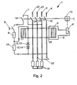
- Fig. 2 shows a second preferred embodiment of a residual current circuit breaker 1 according to the invention, which differs from the in Fig. 1 illustrated first preferred embodiment by the further existing third and fourth conductors 21, 22 differs, to which the third and fourth isolating contacts 23, 24 are assigned.
- the second and third conductors 4, 21 are conductively connected on the load-side side of the summation current transformer 2 by means of a bridge 25.
- the further structure of the residual current circuit breaker corresponds Fig. 1 ,
Description
- Die Erfindung betrifft einen Fehlerstromschutzschalter gemäß dem Oberbegriff des Patentanspruches 1.
Fehlerstromschutzschalter sind zum Schutz von Lebewesen und Anlagen vor gefährlichen Fehlerströmen vorgesehen, und müssen gemäß einschlägiger internationaler, nationaler bzw. regionaler Vorschriften beim Auftreten eines Fehlerstromes, welcher zwischen dem halben Bemessungsfehlerstrom und dem Bemessungsfehlerstrom liegen, auslösen. - Fehlerstromschutzschalter müssen weiters gemäß einschlägiger internationaler, nationaler bzw. regionaler Vorschriften eine Prüfeinrichtung zur Prüfung der Funktionstauglichkeit der Fehlerstromauslösung aufweisen. Eine derartige Prüfeinrichtung umfasst in der Regel einen Prüfwiderstand und einen Prüftaster, wobei bei Betätigung des Prüftasters ein Prüfstromkreis geschlossen wird, und derart ein simulierter Fehlerstrom von einem Leiter zu einem anderen Leiter am Summenstromwandler vorbei erzeugt wird. Sofern der Fehlerstromschutzschalter ordnungsgemäß funktioniert, wird dieser ausgelöst und die Trennkontakte des Fehlerstromschutzschalters durchtrennen die Leiter eines zu schützenden Netzes.
- Gemäß Vorschrift muss die durch die Betätigung der Prüfeinrichtung hervorgerufene Durchflutung im Summenstromwandler kleiner als das 2,5fache der vom Bemessungsfehlerstrom erzeugten Durchflutung sein. Bei einem Fehlerstromschutzschalter mit einem Bemessungsfehlerstrom von 30mA dürfen daher, gemäß Vorschrift, bei Bemessungsspannung bis zu 75mA fließen. Ein bei Betätigung der Prüfeinrichtung auslösender Fehlerstromschutzschalter muss daher nicht zwangsläufig auch beim Auftreten eines wesentlich geringeren tatsächlichen Fehlerstromes noch sicher auslösen.
Der Prüfstromkreis muss weiters über einem weiteren Bereich an Versorgungsspannungen zuverlässig arbeiten. So muss der Prüfstromkreis noch bei Versorgungsspannungen von 85% der Bemessungsspannung arbeiten, sowie bei den üblichen Schwankungen der Versorgungs- bzw. Netzspannung von 10%. Weiters gibt es vierpolige Fehlerstromschutzschalter, welche auch als zweipolige Fehlerstromschutzschalter verwendet werden dürften. Daraus resultiert, dass sich bei einem Prüfstromkreis, welcher derart dimensioniert ist, dass der durch diesen simulierte Fehlerstrom bei 85% der Bemessungsspannung dem Bemessungsfehlerstrom entspricht, der simulierte Fehlerstrom bei der maximal zulässigen Versorgungsspannung um 225% erhöht. Ein Fehlerstromschutzschalter, welcher aufgrund eines erfolgreichen Tests mit einem derartig hohen simulierten Fehlerstrom als funktionssicher befunden wird, stellt daher möglicherweise eine Gefährdung für Lebewesen und Anlagen dar, da daraus nicht sicher auf die Funktion des Fehlerstromschutzschalters beim Bemessungsfehlerstrom geschlossen werden kann. -
GB 2 238 921 A - Aufgabe der Erfindung ist es daher einen Fehlerstromschutzschalter der eingangs genannten Art anzugeben, mit welchem die genannten Nachteile vermieden werden können, und bei welchem die Funktionstauglichkeit der Fehlerstromauslösung genauer überprüft werden kann, und welcher einen einfachen Aufbau aufweist.
Erfindungsgemäß wird dies durch die Merkmale des Patentanspruches 1 erreicht. - Dadurch kann die Funktionstauglichkeit der Fehlerstromauslösung eines erfindungsgemäßen Fehlerstromschutzschalters exakter als bisher überprüft werden. Dadurch kann erreicht werden, dass der beim Betätigen des Prüftasters erzeugte simulierte Fehlerstrom in Abhängigkeit der am Fehlerstromschutzschalter tatsächlich anliegenden Versorgungsspannung lediglich in einem Bereich von etwa 10 % schwankt, im Gegensatz zu Schwankungen von über 200% gemäß dem eingangs dargelegten Stand der Technik. Dadurch kann nach einem erfolgreichen Test des Fehlerstromschutzschalters darauf geschlossen werden, dass der betreffende Fehlerstromschutzschalter auch im tatsächlich auftretenden Fehlerfall funktioniert und auch tatsächlichen Auslösen wird. Dadurch können schadhafte Fehlerstromschutzschalter als solche erkannt und ausgetauscht werden. Dadurch kann die Sicherheit von Lebewesen und Anlagen erheblich erhöht werden.
Ein erfindungsgemäßer Fehlerstromschutzschalter weist weiters einen sehr einfachen Aufbau auf. Dadurch sind die vorstehend angeführten vorteilhaften Wirkungen einfach umsetzbar und verursachen nur geringe Zusatzkosten. Dadurch kann die Verbreitung der gegenständlichen Erfindung gefördert werden, wodurch die Sicherheit einer Vielzahl elektrischer Anlagen erhöht werden kann. Durch den einfachen Aufbau ist es möglich den Prüfstromkreis vollständig netzspannungsunabhängig auszuführen, wodurch dieser sehr ausfallsicher ist, und weiters in allen Ländern dieser Erde zugelassen ist.
Die Unteransprüche, welche ebenso wie der Patentanspruch 1 gleichzeitig einen Teil der Beschreibung bilden, betreffen weitere vorteilhafte Ausgestaltungen der Erfindung. - Die Erfindung wird unter Bezugnahme auf die beigeschlossenen Zeichnungen, in welchen lediglich bevorzugte Ausführungsformen beispielhaft dargestellt sind, näher beschrieben. Dabei zeigt:
-
Fig. 1 ein schematischer Stromlaufplan einer ersten bevorzugten Ausführungsform eines erfindungsgemäßen Fehlerstromschutzschalters, und -
Fig. 2 ein schematischer Stromlaufplan einer zweiten bevorzugten Ausführungsform eines erfindungsgemäßen Fehlerstromschutzschalters. - Die
Fig. 1 und2 zeigen bevorzugte Ausführungsformen eines Fehlerstromschutzschalters 1, umfassend wenigstens einen Summenstromwandler 2 durch welchen wenigstens ein erster Leiter 3 und ein zweiter Leiter 4 eines zu schützenden elektrischen Netzes geführt sind, wobei auf dem Summenstromwandler 2 wenigstens eine Sekundärwicklung 5 angeordnet ist, wobei die Sekundärwicklung 5 schaltungstechnisch mit einem Auslöser 6 verbunden ist, wobei der erste Leiter 3 mittels eines Prüfstromkreises 7 mit dem zweiten Leiter 4 verbunden ist, welcher Prüfstromkreis 7 wenigstens einen ersten Prüfwiderstand 8 sowie einen Prüftaster 9 aufweist, wobei der Prüfstromkreis 7 einen zweiten Prüfwiderstand 10 aufweist, welcher zu dem ersten Prüfwiderstand 8 schaltungstechnisch seriell angeordnet ist, wobei der zweite Prüfwiderstand 10 durch eine Nebenschlussleitung 11 überbrückt ist, wobei die Nebenschlussleitung 11 durch den Summenstromwandler 2 geführt ist, und wobei schaltungstechnisch in der Nebenschlussleitung 11 wenigstens ein erster spannungsabhängiger Widerstand 12 angeordnet ist. - Dadurch kann die Funktionstauglichkeit der Fehlerstromauslösung eines erfindungsgemäßen Fehlerstromschutzschalters 1 exakter als bisher überprüft werden. Dadurch kann erreicht werden, dass der beim Betätigen des Prüftasters 9 erzeugte simulierte Fehlerstrom in Abhängigkeit der am Fehlerstromschutzschalter 1 tatsächlich anliegenden Versorgungsspannung lediglich in einem Bereich von etwa 10 % schwankt, im Gegensatz zu Schwankungen von über 200% gemäß dem eingangs dargelegten Stand der Technik. Dadurch kann nach einem erfolgreichen Test des Fehlerstromschutzschalters 1 darauf geschlossen werden, dass der betreffende Fehlerstromschutzschalter 1 auch im tatsächlich auftretenden Fehlerfall funktioniert und auch tatsächlichen Auslösen wird. Dadurch können schadhafte Fehlerstromschutzschalter 1 als solche erkannt und ausgetauscht werden. Dadurch kann die Sicherheit von Lebewesen und Anlagen erheblich erhöht werden.
- Ein erfindungsgemäßer Fehlerstromschutzschalter 1 weist weiters einen sehr einfachen Aufbau auf. Dadurch sind die vorstehend angeführten vorteilhaften Wirkungen einfach umsetzbar und verursachen nur geringe Zusatzkosten. Dadurch kann die Verbreitung der gegenständlichen Erfindung gefördert werden, wodurch die Sicherheit einer Vielzahl elektrischer Anlagen erhöht werden kann. Durch den einfachen Aufbau ist es möglich den Prüfstromkreis 7 vollständig netzspannungsunabhängig auszuführen, wodurch dieser sehr ausfallsicher ist, und weiters in allen Ländern dieser Erde einsetzbar ist.
- Bei einem erfindungsgemäßen Fehlerstromschutzschalter 1 kann es sich um jede Art eines Fehlerstromschutzschalters 1 handeln, welcher insbesondere weitere Funktionalitäten und Baugruppen aufweisen kann, als die in der gegenständlichen Erfindung beschriebenen. Wie in den
Fig. 1 und2 dargestellt sind erfindungsgemäße Fehlerstromschutzschalter 1 insbesondere zur Verwendung an einem elektrischen Netz mit zwei bzw. vier Leitern 3, 4, 21, 22 vorgesehen. Es können jedoch Ausführungsformen mit jeder vorgebbaren Anzahl an Leitungen bzw. Leitern eines elektrischen Energieversorgungsnetzes bzw. Energieverteilungsnetzes vorgesehen sein. - Ein erfindungsgemäßer Fehlerstromschutzschalter 1 weist - in an sich bekannter Weise - wenigstens einen Summenstromwandler 2 mit einem Wandlerkern, umfassend einen Magnetwerkstoff, auf, durch welchen wenigstens der erste und zweite Leiter 3, 4 als Primärwicklung geführt sind. Die Bezeichnung "durch den Summenstromwandler geführt" bezieht sich dabei, sowie der weiteren Beschreibung der Erfindung, auf die übliche Ausführung des Summenstromwandlers mit einem ringförmigen Wandlerkern, welcher eine Öffnung aufweist, durch welche die betreffenden Leiter 3, 4, 21, 22 geführt sind. Bevorzugt sind diese Leiter 3, 4, 21, 22 weiters wenigstens einmal um den Querschnitt dieses "Rings" herumgeführt bzw. gewickelt.
- Auf dem Summenstromwandler 2 ist weiters eine Sekundärwicklung 5 zur Detektion eines Fehlerstromsignals angeordnet, welche bevorzugt durch einen mehrmals um den Querschnitt des "Rings" gewickelten Leiter, etwa einem dünnen Draht, gebildet ist. Die Sekundärwicklung 5 ist schaltungstechnisch wenigstens mittelbar mit einem Auslöser 6 verbunden, welcher bevorzugt als Permanentmagnetauslöser ausgebildet ist, wodurch eine besonders sichere und schnelle Ansprache des Fehlerstromschutzschalters 1 erreicht werden kann. Der Auslöser 6 wirkt mechanisch über ein Schaltschloss 15 auf die Trennkontakte, was in den
Fig. 1 und2 durch eine punktierte Linie dargestellt ist. Beim Auftreten eines gefährlichen Fehlerstromes, wird ein entsprechendes Fehlerstromsignal in der Sekundärwicklung 5 erzeugt, und der Auslöser 6 wirkt auf die Trennkontakte 17, 18, 19, 23, 24, welche geöffnet werden, und den ersten und zweiten Leiter 3, 4 bzw. gegebenenfalls den dritten und vierten Leiter 21, 22 durchtrennen. Es können auch hievon abweichende Ausgestaltungen eines Auslösers 6, etwa ein netzspannungsabhängiger Auslöser, vorgesehen sein. - Ein erfindungsgemäßer Fehlerstromschutzschalter 1 weist weiters einen Prüfstromkreis 7 auf, welcher dazu ausgebildet und vorgesehen ist, einen simulierten Fehlerstrom zu erzeugen. Der Prüfstromkreis 7 verbindet dabei den ersten Leiter 3 mit dem zweiten Leiter 4, wobei diese Verbindungsleitung nicht durch den Summenstromwandler 5, sondern "außen" an diesem vorbei geführt ist. Der Prüfstromkreis 7 ist im normalen Betrieb des Fehlerstromschutzschalters 1 nicht geschlossen, es fließt daher kein Strom in diesem Prüfstromkreis 7. Zum Schließen des Prüfstromkreises 7 weist dieser einen Prüftaster 9 auf. Weiters weist der Prüfstromkreis 7 wenigstens einen ersten Prüfwiderstand 8 auf. Als Prüfwiderstand 8 im Sinne der gegenständlichen Erfindung wird ein Widerstand bezeichnet, welcher im Wesentlichen als rein ohmscher Widerstand wirkt, bzw. wenigstens bei der Frequenz des zu schützenden Netzes als rein ohmscher Widerstand wirkt.
- Der Prüfstromkreis 7 weist weiters gemäß den in den
Fig. 1 und2 dargestellten bevorzugten Ausführungsformen einen sog. fünften Trennkontakt 19 auf, welcher mechanisch mit dem Schaltschloss 15 bzw. den weiteren Trennkontakten 17, 18, 23, 24 verbunden ist, und bei einem Öffnen der ersten, zweiten, dritten bzw. vierten Trennkontakte 17, 18, 23, 24 ebenfalls geöffnet wird. Dadurch kann verhindert werden, dass bei Betätigung des Prüftasters 9 und bereits erfolgter Auslösung des Fehlerstromschutzschalters 1 weiter Strom über den Prüfstromkreis 7 und den Prüfwiderstand 8 fließt. Ein derartiger weiterhin fließender Strom würde zu erheblichen Verlustleitungen an dem Prüfwiderstand 8 führen, welche zur thermischen Zerstörung des bzw. der Prüfwiderstände 8, 10 führen könnte. Durch den fünften Trennkontakt 19 kann dies sicher verhindert werden, und der erste Prüfwiderstand 8 bzw. der zweite Prüfwiderstand 10 kann, hinsichtlich dessen zulässigen Verlustleistung klein gewählt werden. - Erfindungsgemäß ist vorgesehen, dass der Prüfstromkreis 7 einen zweiten Prüfwiderstand 10 aufweist. Dieser zweite Prüfwiderstand 10 ist bevorzugt ebenfalls als ohmscher Widerstand ausgebildet. Der zweite Prüfwiderstand 10 ist schaltungstechnisch seriell zu dem ersten Prüfwiderstand 8 in dem Prüfstromkreis 7 angeordnet. Erfindungsgemäß ist weiters vorgesehen, dass der zweite Prüfwiderstand 10 durch eine Nebenschlussleitung 11 überbrückt ist. Diese Nebenschlussleitung 11 ist durch den Summenstromwandler 2 geführt, daher durch die Öffnung eines ringförmig ausgebildeten Summenstromwandlers 2. In der Nebenschlussleitung 11 ist schaltungstechnisch wenigstens ein erster spannungsabhängiger Widerstand 12 angeordnet.
- Als spannungsabhängiger Widerstand 12 ist bevorzugt jede Art eines Widerstandes vorgesehen, welcher bei einer anliegenden Spannung unterhalb einer bestimmten Grenzspannung einen hohen, insbesondere einen sehr hohen, Widerstand aufweist, und oberhalb dieser Grenzspannung einen sehr geringen Widerstand. In der Praxis kann diese Grenzspannung auch als Grenzspannungsbereich mit einem gewissen Übergangsbereich des Widerstandes ausgebildet sein. Bevorzugt ist der wenigstens eine erste spannungsabhängige Widerstand 12 als Varistor und/oder als Suppressordiode und/oder Zener-Diode 13 ausgebildet. Entsprechend der bevorzugten Ausbildungen des wenigstens einen ersten spannungsabhängigen Widerstandes 12 als Halbleiterbauelement wird die sog. Grenzspannung auch als Durchbruchsspannung bezeichnet. Die betreffenden, als bevorzugte Ausführungsformen genannten Bauelemente weisen jeweils unterschiedliche charakteristische Eigenschaften, wie etwa Strom/Spannungs-Verläufe, Durchbruchsspannungen, Spannungsabfälle und dergleichen, auf. Je nach konkretem Anwendungsfall kann daher einem der bevorzugten Bauelemente der Vorrang gegeben werden.
- Durch den erfindungsgemäßen schaltungstechnischen Aufbau kann erreicht werden, dass bis zu einem bestimmten vorgebbaren Spannungsabfall am zweiten Prüfwiderstand 10, daher bis zum Erreichen der Durchbruchsspannung, die Nebenschlussleitung hochohmig bzw. im Wesentlichen nicht leitend ist. In diesem Fall arbeitet der Prüfstromkreis 7 wie an sich bekannt, wobei der erste und zweite Prüfwiderstand 8, 10 wie ein Einzelwiderstand wirken. Sobald der Spannungsabfall am zweiten Prüfwiderstand 10 die Durchbruchsspannung des ersten spannungsabhängigen Widerstands 12 erreicht bzw. überschreitet, wird dieser erste spannungsabhängige Widerstand 12 niederohmig und bildet eine Parallelschaltung zum zweiten Prüfwiderstand 10. Dadurch, dass die Nebenschlussleitung 11 durch den Summenstromwandler 5 geführt ist, wird ein Teil des simulierten Fehlerstromes, welcher durch den ersten Prüfwiderstand 8 fließt, wieder durch den Summenstromwandler 2 geführt, weshalb dieser Teilstrom nicht als Fehlerstrom detektiert wird. Dadurch kann erreicht werden, dass der tatsächlich durch die Sekundärwicklung 5 detektierte Fehlerstrom - bei steigender Spannungsdifferenz zwischen dem ersten und dem zweiten Leiter 3, 4 nicht weiter ansteigt, sondern auf einem relativ konstanten Wert bzw. Bereich beschränkt bleibt. Aufgrund des Restwiderstandes, welcher der spannungsabhängige Widerstand 12, 14 in dessen durchgeschalteten Zustand weiterhin aufweist, bzw. des Spannungsabfalls an der Halbleiterübergangsschicht, fließt auch weiterhin ein Teil des simulierten Fehlerstromes durch den zweiten Prüfwiderstand 10 und an dem Summenstromwandler 2 vorbei.
- Über die Größe des ersten und des zweiten Prüfwiderstandes 8, 10, sowie gegebenenfalls die Wahl wenigstens des ersten spannungsabhängigen Widerstandes 12, kann die Größe bzw. Höhe des simulierten Fehlerstromanteils vorgegeben werden, welcher über den zweiten Prüfwiderstand 10 fließt, und tatsächlich als Fehlerstrom zur Detektion durch die Sekundärwicklung 5 bereitsteht. Gemäß einer ersten bevorzugten Ausbildung des ersten und des zweiten Prüfwiderstandes 8, 10 ist etwa vorgesehen, dass der erste Prüfwiderstand 8 einen Wert von 15k Ohm aufweist, und der zweite Prüfwiderstand 10 einen Wert von 560 Ohm. Gemäß einer zweiten bevorzugten Ausbildung des ersten und des zweiten Prüfwiderstandes 8, 10 ist etwa vorgesehen, dass der erste Prüfwiderstand 8 einen Wert von 4k7 Ohm aufweist, und der zweite Prüfwiderstand 10 einen Wert von 1k5 Ohm.
- In Weiterbindung der gegenständlichen Erfindung kann weiters vorgesehen sein, dass in der Nebenschlussleitung 11 schaltungstechnisch seriell zu dem wenigstens einen ersten spannungsabhängigen Widerstand 12 ein Zusatzwiderstand angeordnet ist. Dieser Zusatzwiderstand ist vorzugsweise als herkömmlicher ohmscher Widerstand ausgebildet. Dadurch kann der Spannungsabfall über die gesamte Nebenschlussleitung 11 erhöht werden, und dadurch der über den zweiten Prüfwiderstand 10 fließende simulierte Fehlerstrom weiter vorgebbar beeinflusst bzw. eingestellt werden.
- Gemäß den in den
Fig. 1 und2 dargestellten, besonders bevorzugten ersten und zweiten Ausführungsform der gegenständlichen Erfindung ist vorgesehen, dass ein zweiter spannungsabhängiger Widerstand 14 seriell zu dem ersten spannungsabhängigen Widerstand 12 in der Nebenschlussleitung 11 angeordnet ist. Durch einen derartigen zweiten spannungsabhängigen Widerstand 14 kann etwa der Spannungsabfall über die Nebenschlussleitung 11 weiter beeinflusst werden. - Weiters besteht durch einen zweiten spannungsabhängigen Widerstand 14 die Möglichkeit bei unipolaren Bauelementen, wie etwa bei Ausbildung des ersten spannungsabhängigen Widerstands 12 als Zener-Diode, die Möglichkeit den betreffenden Fehlerstromschutzschalter 1 wechselspannungstauglich zu gestalten. In diesem Zusammenhang ist daher weiters vorgesehen, dass der zweite spannungsabhängige Widerstand 14 als Zener-Diode 13 ausgebildet ist. Dabei ist es besonders vorteilhaft, wenn der als Zener-Diode 13 ausgebildete erste spannungsabhängige Widerstand 12 in einer, zum zweiten spannungsabhängigen Widerstand 14 entgegengesetzten Polarität schaltungstechnisch in der Nebenschlussleitung 11 angeordnet ist.
- Nachfolgend werden die erste und zweite bevorzugte Ausführungsform der gegenständlichen Erfindung anhand der
Fig. 1 und2 im Detail beschrieben. -
Figur 1 zeigt eine lediglich besonders bevorzugte erste Ausführungsform eines erfindungsgemäßen Fehlerstromschutzschalters 1 zur netzspannungsunabhängigen Fehlerstromauslösung als schematische Darstellung der funktionellen Baugruppen. Ein derartiger Fehlerstromschutzschalter 1 ist zum Schutz von Anlagen und Menschen vorgesehen, wobei im Falle eines auftretenden gefährlichen Fehlerstromes die an den Fehlerstromschutzschalter 1 angeschlossenen Verbraucher bzw. Last 16 von einem Versorgungsnetz, umfassend den ersten Leiter 3 und den zweiten Leiter 4, getrennt werden. Der Fehlerstromschutzschalter weist Anschlussklemmen, insbesondere Schraubanschlussklemmen, zum Anschluss wenigstens eines ersten und eines zweiten Leiters 3, 4 eines elektrischen Versorgungsnetzes auf. Der dargestellte schematische Stromlaufplan gemäßFig. 1 zeigt eine Ausführungsform mit lediglich einem ersten und einem zweiten Leiter 3, 4. In dem ersten und dem zweiten Leiter 3, 4 sind erste und zweite Trennkontakte 17, 18, daher Schaltkontakte, welche zum Auftrennen bzw. Unterbrechen des ersten bzw. zweiten Leiters 3, 4, sowie zum anschließenden Schließen, vorgesehen bzw. ausgebildet sind, angeordnet. Die beschriebenen und inFig. 1 dargestellten Bauelemente bzw. Baugruppen sind zusammen in einem Isolierstoffgehäuse angeordnet, welches Durchbrechungen wenigstens für die Anschlussklemmen und einen manuell betätigbaren Handschalthebel zum manuellen Öffnen bzw. Schließen der ersten und zweiten Trennkontakte 17, 18 aufweist. Weiters kann vorgesehen sein, dass ein erfindungsgemäßer Fehlerstromschutzschalter 1 weitere - nicht dargestellte bzw. beschriebene - Baugruppen bzw. Bauteile umfasst, etwa eine Schaltstellungsanzeige, eine Auslöseanzeige und dergleichen.Fig. 1 zeigt weiters eine beispielhaft dargestellte Last 16, im Sinne eines elektrischen Verbrauchers. - Erfindungsgemäße Fehlerstromschutzschalter 1 sind bevorzugt als netzspannungsunabhängige Fehlerstromschutzschalter 1 ausgebildet. Die in einem derartigen netzspannungsunabhängigen Fehlerstromschutzschalter 1 zur Detektion eines Fehlerstromes und Auslösung des Fehlerstromschutzschalters 1, daher Trennen der Trennkontakte 17, 18 angeordneten Baugruppen beziehen deren zum Auslösen notwendige Energie vollständig aus dem Fehlerstrom bzw. dem zu diesem proportionalen Fehlerstromsignal in der Sekundärwicklung 5, und weisen daher keine aktiven elektronischen Bauteile, wie etwa Transistoren und/oder Operationsverstärker, und keine Netzteile zur Versorgung derartiger aktiver Bauelemente auf.
- Der Prüfstromkreis 7 ist mit dem ersten Leiter 3 verbunden und verläuft bis zum bereits besprochenen fünften Trennkontakt 19, welcher leitend mit dem Prüftaster 9 verbunden ist. Der Prüftaster 9 ist weiters leitend mit dem ersten Prüfwiderstand 8 verbunden, dessen anderer Anschluss sowohl mit dem zweiten Prüfwiderstand 10 sowie der Nebenschlussleitung 11 leitend verbunden ist. Der weitere Anschluss des zweiten Prüfwiderstandes 10 ist leitend sowohl mit dem zweiten Leiter 4, als auch mit der Nebenschlussleitung 11 verbunden. In der Nebenschlussleitung 11 sind ein erster und ein zweiter spannungsabhängiger Widerstand 12, 14 angeordnet, welche beide als Zener-Diode 13 ausgebildet sind. Die betreffenden ZenerDioden 13 sind dabei gegenpolar in der Nebenschlussleitung 11 angeordnet.
-
Fig. 2 zeigt eine zweite bevorzugte Ausführungsform eines erfindungsgemäßen Fehlerstromschutzschalters 1, welche sich von der inFig. 1 dargestellten ersten bevorzugten Ausführungsform durch die weiters vorhandenen dritten und vierten Leiter 21, 22 unterscheidet, welchen die dritten und vierten Trennkontakte 23, 24 zugeordnet sind. Der zweite und der dritte Leiter 4, 21 sind auf der lastseitigen Seite des Summenstromwandlers 2 mittels eines Brücke 25 leitend verbunden. Der weitere Aufbau des Fehlerstromschutzschalters entsprichtFig. 1 . - Weitere erfindungsgemäße Ausführungsformen weisen lediglich einen Teil der beschriebenen Merkmale auf, wobei jede Merkmalskombination, insbesondere auch von verschiedenen beschriebenen Ausführungsformen, vorgesehen sein kann.
Claims (9)
- Fehlerstromschutzschalter (1), umfassend wenigstens einen Summenstromwandler (2) durch welchen wenigstens ein erster Leiter (3) und ein zweiter Leiter (4) eines zu schützenden elektrischen Netzes geführt sind, wobei auf dem Summenstromwandler (2) wenigstens eine Sekundärwicklung (5) angeordnet ist, wobei die Sekundärwicklung (5) schaltungstechnisch mit einem Auslöser (6) verbunden ist, wobei der erste Leiter (3) mittels eines Prüfstromkreises (7) mit dem zweiten Leiter (4) verbunden ist, welcher Prüfstromkreis (7) wenigstens einen ersten Prüfwiderstand (8) sowie einen Prüftaster (9) aufweist, wobei der Prüfstromkreis (7) einen zweiten Prüfwiderstand (10) aufweist, welcher zu dem ersten Prüfwiderstand (8) schaltungstechnisch seriell angeordnet ist, wobei der zweite Prüfwiderstand (10) durch eine Nebenschlussleitung (11) überbrückt ist, und wobei schaltungstechnisch in der Nebenschlussleitung (11) wenigstens ein erster spannungsabhängiger Widerstand (12) angeordnet ist, dadurch gekennzeichnet, dass die Nebenschlussleitung (11) durch den Summenstromwandler (2) geführt ist.
- Fehlerstromschutzschalter (1) nach Anspruch 1, dadurch gekennzeichnet, dass der erste spannungsabhängige Widerstand (12) als Varistor ausgebildet ist.
- Fehlerstromschutzschalter (1) nach Anspruch 1, dadurch gekennzeichnet, dass der erste spannungsabhängige Widerstand (12) als Suppressordiode ausgebildet ist.
- Fehlerstromschutzschalter (1) nach Anspruch 1, dadurch gekennzeichnet, dass der erste spannungsabhängige Widerstand (12) als Zener-Diode (13) ausgebildet ist.
- Fehlerstromschutzschalter (1) nach einem der Ansprüche 1 bis 4, dadurch gekennzeichnet, dass ein zweiter spannungsabhängiger Widerstand (14) seriell zu dem ersten spannungsabhängigen Widerstand (12) in der Nebenschlussleitung (11) angeordnet ist.
- Fehlerstromschutzschalter (1) nach Anspruch 5, dadurch gekennzeichnet, dass der zweite spannungsabhängige Widerstand (14) als Zener-Diode (13) ausgebildet ist.
- Fehlerstromschutzschalter (1) nach Anspruch 6, dadurch gekennzeichnet, dass der als Zener-Diode (13) ausgebildete erste spannungsabhängige Widerstand (12) in einer, zum zweiten spannungsabhängigen Widerstand (14) entgegengesetzten Polarität schaltungstechnisch in der Nebenschlussleitung (11) angeordnet ist.
- Fehlerstromschutzschalter (1) nach einem der Ansprüche 1 bis 7, dadurch gekennzeichnet, dass in der Nebenschlussleitung (11) schaltungstechnisch seriell zu dem wenigstens einen ersten spannungsabhängigen Widerstand ein Zusatzwiderstand angeordnet ist.
- Fehlerstromschutzschalter (1) nach einem der Ansprüche 1 bis 8, dadurch gekennzeichnet, dass der Fehlerstromschutzschalter (1) als netzspannungsunabhängiger Fehlerstromschutzschalter (1) ausgebildet ist.
Priority Applications (1)
| Application Number | Priority Date | Filing Date | Title |
|---|---|---|---|
| PL11714674T PL2548214T3 (pl) | 2010-03-19 | 2011-03-09 | Wyłącznik różnicowoprądowy |
Applications Claiming Priority (2)
| Application Number | Priority Date | Filing Date | Title |
|---|---|---|---|
| AT0045010A AT509838A2 (de) | 2010-03-19 | 2010-03-19 | Fehlerstromschutzschalter |
| PCT/AT2011/000114 WO2011113072A1 (de) | 2010-03-19 | 2011-03-09 | Fehlerstromschutzschalter |
Publications (2)
| Publication Number | Publication Date |
|---|---|
| EP2548214A1 EP2548214A1 (de) | 2013-01-23 |
| EP2548214B1 true EP2548214B1 (de) | 2014-01-15 |
Family
ID=44072793
Family Applications (1)
| Application Number | Title | Priority Date | Filing Date |
|---|---|---|---|
| EP11714674.6A Active EP2548214B1 (de) | 2010-03-19 | 2011-03-09 | Fehlerstromschutzschalter |
Country Status (11)
| Country | Link |
|---|---|
| US (2) | US8624694B2 (de) |
| EP (1) | EP2548214B1 (de) |
| CN (1) | CN102870186B (de) |
| AT (1) | AT509838A2 (de) |
| BR (1) | BR112012023632A2 (de) |
| CL (1) | CL2012002557A1 (de) |
| DK (1) | DK2548214T3 (de) |
| ES (1) | ES2449477T3 (de) |
| PL (1) | PL2548214T3 (de) |
| UA (1) | UA107220C2 (de) |
| WO (1) | WO2011113072A1 (de) |
Families Citing this family (4)
| Publication number | Priority date | Publication date | Assignee | Title |
|---|---|---|---|---|
| EP2676284B1 (de) * | 2011-02-16 | 2017-06-07 | Eaton Industries (Austria) GmbH | Fehlerstromschutzschalter |
| US10361555B2 (en) | 2014-07-16 | 2019-07-23 | Eaton Intelligent Power Limited | Device to reduce residual current |
| FR3029350B1 (fr) * | 2014-12-01 | 2016-12-23 | Hager-Electro Sas | Dispositif de protection differentielle |
| DE102017217267A1 (de) | 2017-09-28 | 2018-07-26 | Siemens Aktiengesellschaft | Fehlerstromschutzschalter und Prüfstromkreis |
Family Cites Families (16)
| Publication number | Priority date | Publication date | Assignee | Title |
|---|---|---|---|---|
| DE3230557A1 (de) | 1982-08-17 | 1984-02-23 | Siemens AG, 1000 Berlin und 8000 München | Fehlerstromschutzschalter |
| GB2238921A (en) | 1989-12-07 | 1991-06-12 | Wellong Trading Ltd | Ground fault circuit interrupter |
| DE9116917U1 (de) | 1991-07-08 | 1994-07-21 | Siemens Ag | Fehlerstromschutzschalter |
| ATE143751T1 (de) | 1991-07-12 | 1996-10-15 | Maier & Cie C | Elektronische auslöseschaltung für einen fi- schutzschalter |
| DE4439072C2 (de) | 1994-11-02 | 1996-09-26 | Kopp Heinrich Ag | Schutzschalter für die Abschaltung von Fehlerströmen beliebiger Stromart |
| JP3559165B2 (ja) | 1998-05-25 | 2004-08-25 | 三菱電機株式会社 | 漏電遮断器 |
| EP1150412A1 (de) | 2000-04-25 | 2001-10-31 | Siemens Aktiengesellschaft | Fehlerstrom-Schutzschalter und Verfahren zum Überprüfen der Funktionsfähigkeit eines Fehlerstrom-Schutzschalters |
| US7026895B2 (en) * | 2003-01-23 | 2006-04-11 | Leviton Manufacturing Co., Inc. | GFCI receptacle having plug blocking means |
| DE60317183T2 (de) * | 2003-07-15 | 2008-06-26 | Gamesa Innovation & Technology, S.L. Unipersonal | Steuer- und Schutzgerät für ein doppelgespeistes Induktionsgeneratorsystem |
| CN2704941Y (zh) * | 2004-05-21 | 2005-06-15 | 上海益而益电器制造有限公司 | 一种具有反向接线保护功能的漏电保护插座 |
| CN100433224C (zh) * | 2004-09-01 | 2008-11-12 | 陈贵 | 具有反向接线保护功能的接地故障线路断路器 |
| US7619861B2 (en) * | 2004-09-29 | 2009-11-17 | Pass & Seymour, Inc. | Protective device having a thin construction |
| US20100191306A1 (en) * | 2006-01-25 | 2010-07-29 | Greatbatch Ltd. | Transient voltage suppression circuit for an implanted rfid chip |
| GB0607331D0 (en) * | 2006-04-12 | 2006-05-24 | Deepstream Technologies Ltd | Residual current device having voltage dependent and voltage independent modes of operation |
| CN101227076B (zh) * | 2008-01-14 | 2010-06-23 | 通领科技集团有限公司 | 接地故障断路器的故障自检电路 |
| AT506346B1 (de) | 2008-02-14 | 2010-01-15 | Moeller Gebaeudeautomation Gmb | Fehlerstromschutzschalter |
-
2010
- 2010-03-19 AT AT0045010A patent/AT509838A2/de not_active Application Discontinuation
-
2011
- 2011-03-09 WO PCT/AT2011/000114 patent/WO2011113072A1/de active Application Filing
- 2011-03-09 EP EP11714674.6A patent/EP2548214B1/de active Active
- 2011-03-09 BR BR112012023632A patent/BR112012023632A2/pt not_active IP Right Cessation
- 2011-03-09 CN CN201180014729.9A patent/CN102870186B/zh not_active Expired - Fee Related
- 2011-03-09 US US13/635,783 patent/US8624694B2/en not_active Expired - Fee Related
- 2011-03-09 PL PL11714674T patent/PL2548214T3/pl unknown
- 2011-03-09 UA UAA201212012A patent/UA107220C2/uk unknown
- 2011-03-09 ES ES11714674.6T patent/ES2449477T3/es active Active
- 2011-03-09 DK DK11714674.6T patent/DK2548214T3/en active
- 2011-03-18 US US13/051,444 patent/US8749941B2/en not_active Expired - Fee Related
-
2012
- 2012-09-14 CL CL2012002557A patent/CL2012002557A1/es unknown
Also Published As
| Publication number | Publication date |
|---|---|
| BR112012023632A2 (pt) | 2017-03-21 |
| DK2548214T3 (en) | 2014-02-24 |
| UA107220C2 (uk) | 2014-12-10 |
| CL2012002557A1 (es) | 2013-08-09 |
| US8624694B2 (en) | 2014-01-07 |
| WO2011113072A1 (de) | 2011-09-22 |
| US8749941B2 (en) | 2014-06-10 |
| AT509838A2 (de) | 2011-11-15 |
| ES2449477T3 (es) | 2014-03-19 |
| EP2548214A1 (de) | 2013-01-23 |
| PL2548214T3 (pl) | 2014-04-30 |
| US20120069484A1 (en) | 2012-03-22 |
| CN102870186B (zh) | 2015-07-22 |
| US20130120091A1 (en) | 2013-05-16 |
| CN102870186A (zh) | 2013-01-09 |
Similar Documents
| Publication | Publication Date | Title |
|---|---|---|
| EP2253004B1 (de) | Fehlerstromschutzschalter | |
| AT405350B (de) | Schutzschaltungsanordnung für überspannungsableiter | |
| EP2622622B1 (de) | Fehlerstromschutzschalter | |
| WO2007121492A1 (de) | Schalteinrichtung | |
| AT405114B (de) | Ableitertrennschalter | |
| EP2559127B1 (de) | Fehlerstromschutzschalter | |
| EP2548214B1 (de) | Fehlerstromschutzschalter | |
| AT505799B1 (de) | Fehlerstromschutzschalter | |
| EP3347959B1 (de) | Anordnung zur sicheren, von schaltgeräten oder vorsicherungen unabhängigen, netzseitigen abtrennung von überspannungsschutzeinrichtungen im fall kritischer betriebszustände | |
| DE19946098C2 (de) | Fehlerstromschutzeinrichtung | |
| AT517200B1 (de) | Fehlerstromschutzschalter | |
| AT406208B (de) | Fi-schutzschalter mit überspannungsauslösung | |
| WO2014187952A1 (de) | Fehlerstromschutzschalter | |
| EP3437169A1 (de) | Schaltungsanordnung zum schutz von an einem mehrphasigen netz angeschlossenen verbrauchern mit unter- und überspannungsabschaltfunktion | |
| DE19944409A1 (de) | Verfahren zur fehlerartabhängig empfindlichen Auslösung einer Differenzstromschutzeinrichtung, und Differenzstromschutzeinrichtung mit fehlerartabhängiger Empfindlichkeit | |
| WO2014083190A1 (de) | Schaltgeraet | |
| DE102021210828A1 (de) | Schutzschaltgerät und Verfahren | |
| DE102021210816A1 (de) | Schutzschaltgerät | |
| DE4343560A1 (de) | Fehlerstromschutzschalter | |
| DE102015004541A1 (de) | Fehlerstrom-Schutzeinrichtung mit zusätzlicher Auslösefunktion |
Legal Events
| Date | Code | Title | Description |
|---|---|---|---|
| PUAI | Public reference made under article 153(3) epc to a published international application that has entered the european phase |
Free format text: ORIGINAL CODE: 0009012 |
|
| 17P | Request for examination filed |
Effective date: 20121005 |
|
| AK | Designated contracting states |
Kind code of ref document: A1 Designated state(s): AL AT BE BG CH CY CZ DE DK EE ES FI FR GB GR HR HU IE IS IT LI LT LU LV MC MK MT NL NO PL PT RO RS SE SI SK SM TR |
|
| DAX | Request for extension of the european patent (deleted) | ||
| GRAP | Despatch of communication of intention to grant a patent |
Free format text: ORIGINAL CODE: EPIDOSNIGR1 |
|
| RIC1 | Information provided on ipc code assigned before grant |
Ipc: H01H 83/04 20060101AFI20130723BHEP Ipc: H01H 83/14 20060101ALN20130723BHEP |
|
| INTG | Intention to grant announced |
Effective date: 20130806 |
|
| GRAS | Grant fee paid |
Free format text: ORIGINAL CODE: EPIDOSNIGR3 |
|
| GRAA | (expected) grant |
Free format text: ORIGINAL CODE: 0009210 |
|
| AK | Designated contracting states |
Kind code of ref document: B1 Designated state(s): AL AT BE BG CH CY CZ DE DK EE ES FI FR GB GR HR HU IE IS IT LI LT LU LV MC MK MT NL NO PL PT RO RS SE SI SK SM TR |
|
| REG | Reference to a national code |
Ref country code: GB Ref legal event code: FG4D Free format text: NOT ENGLISH Ref country code: CH Ref legal event code: EP |
|
| REG | Reference to a national code |
Ref country code: AT Ref legal event code: REF Ref document number: 650148 Country of ref document: AT Kind code of ref document: T Effective date: 20140215 |
|
| REG | Reference to a national code |
Ref country code: DK Ref legal event code: T3 Effective date: 20140218 Ref country code: RO Ref legal event code: EPE |
|
| REG | Reference to a national code |
Ref country code: NL Ref legal event code: T3 Ref country code: IE Ref legal event code: FG4D Free format text: LANGUAGE OF EP DOCUMENT: GERMAN |
|
| REG | Reference to a national code |
Ref country code: DE Ref legal event code: R096 Ref document number: 502011002053 Country of ref document: DE Effective date: 20140227 |
|
| REG | Reference to a national code |
Ref country code: ES Ref legal event code: FG2A Ref document number: 2449477 Country of ref document: ES Kind code of ref document: T3 Effective date: 20140319 |
|
| REG | Reference to a national code |
Ref country code: NO Ref legal event code: T2 Effective date: 20140115 |
|
| PGFP | Annual fee paid to national office [announced via postgrant information from national office to epo] |
Ref country code: DK Payment date: 20140325 Year of fee payment: 4 |
|
| REG | Reference to a national code |
Ref country code: PL Ref legal event code: T3 |
|
| REG | Reference to a national code |
Ref country code: LT Ref legal event code: MG4D |
|
| PG25 | Lapsed in a contracting state [announced via postgrant information from national office to epo] |
Ref country code: LT Free format text: LAPSE BECAUSE OF FAILURE TO SUBMIT A TRANSLATION OF THE DESCRIPTION OR TO PAY THE FEE WITHIN THE PRESCRIBED TIME-LIMIT Effective date: 20140115 Ref country code: IS Free format text: LAPSE BECAUSE OF FAILURE TO SUBMIT A TRANSLATION OF THE DESCRIPTION OR TO PAY THE FEE WITHIN THE PRESCRIBED TIME-LIMIT Effective date: 20140515 |
|
| PG25 | Lapsed in a contracting state [announced via postgrant information from national office to epo] |
Ref country code: SE Free format text: LAPSE BECAUSE OF FAILURE TO SUBMIT A TRANSLATION OF THE DESCRIPTION OR TO PAY THE FEE WITHIN THE PRESCRIBED TIME-LIMIT Effective date: 20140115 Ref country code: CY Free format text: LAPSE BECAUSE OF FAILURE TO SUBMIT A TRANSLATION OF THE DESCRIPTION OR TO PAY THE FEE WITHIN THE PRESCRIBED TIME-LIMIT Effective date: 20140115 Ref country code: FI Free format text: LAPSE BECAUSE OF FAILURE TO SUBMIT A TRANSLATION OF THE DESCRIPTION OR TO PAY THE FEE WITHIN THE PRESCRIBED TIME-LIMIT Effective date: 20140115 Ref country code: PT Free format text: LAPSE BECAUSE OF FAILURE TO SUBMIT A TRANSLATION OF THE DESCRIPTION OR TO PAY THE FEE WITHIN THE PRESCRIBED TIME-LIMIT Effective date: 20140515 |
|
| PG25 | Lapsed in a contracting state [announced via postgrant information from national office to epo] |
Ref country code: RS Free format text: LAPSE BECAUSE OF FAILURE TO SUBMIT A TRANSLATION OF THE DESCRIPTION OR TO PAY THE FEE WITHIN THE PRESCRIBED TIME-LIMIT Effective date: 20140115 Ref country code: LV Free format text: LAPSE BECAUSE OF FAILURE TO SUBMIT A TRANSLATION OF THE DESCRIPTION OR TO PAY THE FEE WITHIN THE PRESCRIBED TIME-LIMIT Effective date: 20140115 Ref country code: HR Free format text: LAPSE BECAUSE OF FAILURE TO SUBMIT A TRANSLATION OF THE DESCRIPTION OR TO PAY THE FEE WITHIN THE PRESCRIBED TIME-LIMIT Effective date: 20140115 |
|
| REG | Reference to a national code |
Ref country code: DE Ref legal event code: R097 Ref document number: 502011002053 Country of ref document: DE |
|
| PG25 | Lapsed in a contracting state [announced via postgrant information from national office to epo] |
Ref country code: LU Free format text: LAPSE BECAUSE OF FAILURE TO SUBMIT A TRANSLATION OF THE DESCRIPTION OR TO PAY THE FEE WITHIN THE PRESCRIBED TIME-LIMIT Effective date: 20140309 Ref country code: EE Free format text: LAPSE BECAUSE OF FAILURE TO SUBMIT A TRANSLATION OF THE DESCRIPTION OR TO PAY THE FEE WITHIN THE PRESCRIBED TIME-LIMIT Effective date: 20140115 |
|
| REG | Reference to a national code |
Ref country code: CH Ref legal event code: PL |
|
| PLBE | No opposition filed within time limit |
Free format text: ORIGINAL CODE: 0009261 |
|
| STAA | Information on the status of an ep patent application or granted ep patent |
Free format text: STATUS: NO OPPOSITION FILED WITHIN TIME LIMIT |
|
| PG25 | Lapsed in a contracting state [announced via postgrant information from national office to epo] |
Ref country code: SK Free format text: LAPSE BECAUSE OF FAILURE TO SUBMIT A TRANSLATION OF THE DESCRIPTION OR TO PAY THE FEE WITHIN THE PRESCRIBED TIME-LIMIT Effective date: 20140115 |
|
| 26N | No opposition filed |
Effective date: 20141016 |
|
| REG | Reference to a national code |
Ref country code: IE Ref legal event code: MM4A |
|
| PG25 | Lapsed in a contracting state [announced via postgrant information from national office to epo] |
Ref country code: CH Free format text: LAPSE BECAUSE OF NON-PAYMENT OF DUE FEES Effective date: 20140331 Ref country code: IE Free format text: LAPSE BECAUSE OF NON-PAYMENT OF DUE FEES Effective date: 20140309 Ref country code: LI Free format text: LAPSE BECAUSE OF NON-PAYMENT OF DUE FEES Effective date: 20140331 |
|
| REG | Reference to a national code |
Ref country code: DE Ref legal event code: R097 Ref document number: 502011002053 Country of ref document: DE Effective date: 20141016 |
|
| PGFP | Annual fee paid to national office [announced via postgrant information from national office to epo] |
Ref country code: RO Payment date: 20150218 Year of fee payment: 5 Ref country code: ES Payment date: 20150323 Year of fee payment: 5 Ref country code: NL Payment date: 20150310 Year of fee payment: 5 |
|
| PG25 | Lapsed in a contracting state [announced via postgrant information from national office to epo] |
Ref country code: SI Free format text: LAPSE BECAUSE OF FAILURE TO SUBMIT A TRANSLATION OF THE DESCRIPTION OR TO PAY THE FEE WITHIN THE PRESCRIBED TIME-LIMIT Effective date: 20140115 |
|
| PGFP | Annual fee paid to national office [announced via postgrant information from national office to epo] |
Ref country code: GB Payment date: 20150224 Year of fee payment: 5 |
|
| PGFP | Annual fee paid to national office [announced via postgrant information from national office to epo] |
Ref country code: BE Payment date: 20150317 Year of fee payment: 5 |
|
| REG | Reference to a national code |
Ref country code: DK Ref legal event code: EBP Effective date: 20150331 |
|
| REG | Reference to a national code |
Ref country code: FR Ref legal event code: PLFP Year of fee payment: 6 |
|
| PG25 | Lapsed in a contracting state [announced via postgrant information from national office to epo] |
Ref country code: MT Free format text: LAPSE BECAUSE OF FAILURE TO SUBMIT A TRANSLATION OF THE DESCRIPTION OR TO PAY THE FEE WITHIN THE PRESCRIBED TIME-LIMIT Effective date: 20140115 |
|
| PG25 | Lapsed in a contracting state [announced via postgrant information from national office to epo] |
Ref country code: SM Free format text: LAPSE BECAUSE OF FAILURE TO SUBMIT A TRANSLATION OF THE DESCRIPTION OR TO PAY THE FEE WITHIN THE PRESCRIBED TIME-LIMIT Effective date: 20140115 Ref country code: DK Free format text: LAPSE BECAUSE OF NON-PAYMENT OF DUE FEES Effective date: 20150331 |
|
| PGFP | Annual fee paid to national office [announced via postgrant information from national office to epo] |
Ref country code: CZ Payment date: 20160226 Year of fee payment: 6 |
|
| PG25 | Lapsed in a contracting state [announced via postgrant information from national office to epo] |
Ref country code: MC Free format text: LAPSE BECAUSE OF FAILURE TO SUBMIT A TRANSLATION OF THE DESCRIPTION OR TO PAY THE FEE WITHIN THE PRESCRIBED TIME-LIMIT Effective date: 20140115 |
|
| PGFP | Annual fee paid to national office [announced via postgrant information from national office to epo] |
Ref country code: FR Payment date: 20160223 Year of fee payment: 6 |
|
| PG25 | Lapsed in a contracting state [announced via postgrant information from national office to epo] |
Ref country code: BG Free format text: LAPSE BECAUSE OF FAILURE TO SUBMIT A TRANSLATION OF THE DESCRIPTION OR TO PAY THE FEE WITHIN THE PRESCRIBED TIME-LIMIT Effective date: 20140115 Ref country code: GR Free format text: LAPSE BECAUSE OF FAILURE TO SUBMIT A TRANSLATION OF THE DESCRIPTION OR TO PAY THE FEE WITHIN THE PRESCRIBED TIME-LIMIT Effective date: 20140416 |
|
| PG25 | Lapsed in a contracting state [announced via postgrant information from national office to epo] |
Ref country code: HU Free format text: LAPSE BECAUSE OF FAILURE TO SUBMIT A TRANSLATION OF THE DESCRIPTION OR TO PAY THE FEE WITHIN THE PRESCRIBED TIME-LIMIT; INVALID AB INITIO Effective date: 20110309 |
|
| PG25 | Lapsed in a contracting state [announced via postgrant information from national office to epo] |
Ref country code: BE Free format text: LAPSE BECAUSE OF NON-PAYMENT OF DUE FEES Effective date: 20160331 |
|
| REG | Reference to a national code |
Ref country code: NL Ref legal event code: MM Effective date: 20160401 |
|
| GBPC | Gb: european patent ceased through non-payment of renewal fee |
Effective date: 20160309 |
|
| PG25 | Lapsed in a contracting state [announced via postgrant information from national office to epo] |
Ref country code: RO Free format text: LAPSE BECAUSE OF NON-PAYMENT OF DUE FEES Effective date: 20160309 |
|
| PG25 | Lapsed in a contracting state [announced via postgrant information from national office to epo] |
Ref country code: NL Free format text: LAPSE BECAUSE OF NON-PAYMENT OF DUE FEES Effective date: 20160401 Ref country code: GB Free format text: LAPSE BECAUSE OF NON-PAYMENT OF DUE FEES Effective date: 20160309 |
|
| PG25 | Lapsed in a contracting state [announced via postgrant information from national office to epo] |
Ref country code: IT Free format text: LAPSE BECAUSE OF NON-PAYMENT OF DUE FEES Effective date: 20160309 |
|
| REG | Reference to a national code |
Ref country code: ES Ref legal event code: FD2A Effective date: 20170427 |
|
| PG25 | Lapsed in a contracting state [announced via postgrant information from national office to epo] |
Ref country code: ES Free format text: LAPSE BECAUSE OF NON-PAYMENT OF DUE FEES Effective date: 20160310 |
|
| PG25 | Lapsed in a contracting state [announced via postgrant information from national office to epo] |
Ref country code: CZ Free format text: LAPSE BECAUSE OF NON-PAYMENT OF DUE FEES Effective date: 20170309 |
|
| PGFP | Annual fee paid to national office [announced via postgrant information from national office to epo] |
Ref country code: TR Payment date: 20150309 Year of fee payment: 5 |
|
| REG | Reference to a national code |
Ref country code: FR Ref legal event code: ST Effective date: 20171130 |
|
| PG25 | Lapsed in a contracting state [announced via postgrant information from national office to epo] |
Ref country code: FR Free format text: LAPSE BECAUSE OF NON-PAYMENT OF DUE FEES Effective date: 20170331 |
|
| PG25 | Lapsed in a contracting state [announced via postgrant information from national office to epo] |
Ref country code: MK Free format text: LAPSE BECAUSE OF FAILURE TO SUBMIT A TRANSLATION OF THE DESCRIPTION OR TO PAY THE FEE WITHIN THE PRESCRIBED TIME-LIMIT Effective date: 20140115 |
|
| PG25 | Lapsed in a contracting state [announced via postgrant information from national office to epo] |
Ref country code: AL Free format text: LAPSE BECAUSE OF FAILURE TO SUBMIT A TRANSLATION OF THE DESCRIPTION OR TO PAY THE FEE WITHIN THE PRESCRIBED TIME-LIMIT Effective date: 20140115 |
|
| REG | Reference to a national code |
Ref country code: DE Ref legal event code: R081 Ref document number: 502011002053 Country of ref document: DE Owner name: EATON INTELLIGENT POWER LIMITED, IE Free format text: FORMER OWNER: EATON INDUSTRIES (AUSTRIA) GMBH, 3943 SCHREMS, AT |
|
| REG | Reference to a national code |
Ref country code: AT Ref legal event code: PC Ref document number: 650148 Country of ref document: AT Kind code of ref document: T Owner name: EATON INTELLIGENT POWER LIMITED, IE Effective date: 20190214 |
|
| PGFP | Annual fee paid to national office [announced via postgrant information from national office to epo] |
Ref country code: IT Payment date: 20190221 Year of fee payment: 19 Ref country code: NO Payment date: 20190227 Year of fee payment: 9 |
|
| PGFP | Annual fee paid to national office [announced via postgrant information from national office to epo] |
Ref country code: AT Payment date: 20190221 Year of fee payment: 9 |
|
| REG | Reference to a national code |
Ref country code: NO Ref legal event code: MMEP |
|
| REG | Reference to a national code |
Ref country code: AT Ref legal event code: MM01 Ref document number: 650148 Country of ref document: AT Kind code of ref document: T Effective date: 20200309 |
|
| PG25 | Lapsed in a contracting state [announced via postgrant information from national office to epo] |
Ref country code: NO Free format text: LAPSE BECAUSE OF NON-PAYMENT OF DUE FEES Effective date: 20200331 Ref country code: AT Free format text: LAPSE BECAUSE OF NON-PAYMENT OF DUE FEES Effective date: 20200309 |
|
| PG25 | Lapsed in a contracting state [announced via postgrant information from national office to epo] |
Ref country code: PL Free format text: LAPSE BECAUSE OF NON-PAYMENT OF DUE FEES Effective date: 20200309 |
|
| PG25 | Lapsed in a contracting state [announced via postgrant information from national office to epo] |
Ref country code: TR Free format text: LAPSE BECAUSE OF NON-PAYMENT OF DUE FEES Effective date: 20160309 |
|
| PGFP | Annual fee paid to national office [announced via postgrant information from national office to epo] |
Ref country code: DE Payment date: 20230221 Year of fee payment: 13 |
|
| P01 | Opt-out of the competence of the unified patent court (upc) registered |
Effective date: 20230521 |