EP2548121B1 - Mlc self-raid flash data protection scheme - Google Patents
Mlc self-raid flash data protection scheme Download PDFInfo
- Publication number
- EP2548121B1 EP2548121B1 EP11756916.0A EP11756916A EP2548121B1 EP 2548121 B1 EP2548121 B1 EP 2548121B1 EP 11756916 A EP11756916 A EP 11756916A EP 2548121 B1 EP2548121 B1 EP 2548121B1
- Authority
- EP
- European Patent Office
- Prior art keywords
- page
- pages
- parity
- group
- flash memory
- Prior art date
- Legal status (The legal status is an assumption and is not a legal conclusion. Google has not performed a legal analysis and makes no representation as to the accuracy of the status listed.)
- Active
Links
Images


Classifications
-
- G—PHYSICS
- G11—INFORMATION STORAGE
- G11C—STATIC STORES
- G11C16/00—Erasable programmable read-only memories
- G11C16/02—Erasable programmable read-only memories electrically programmable
- G11C16/06—Auxiliary circuits, e.g. for writing into memory
- G11C16/22—Safety or protection circuits preventing unauthorised or accidental access to memory cells
-
- G—PHYSICS
- G06—COMPUTING; CALCULATING OR COUNTING
- G06F—ELECTRIC DIGITAL DATA PROCESSING
- G06F12/00—Accessing, addressing or allocating within memory systems or architectures
- G06F12/02—Addressing or allocation; Relocation
-
- G—PHYSICS
- G06—COMPUTING; CALCULATING OR COUNTING
- G06F—ELECTRIC DIGITAL DATA PROCESSING
- G06F11/00—Error detection; Error correction; Monitoring
- G06F11/07—Responding to the occurrence of a fault, e.g. fault tolerance
- G06F11/08—Error detection or correction by redundancy in data representation, e.g. by using checking codes
- G06F11/10—Adding special bits or symbols to the coded information, e.g. parity check, casting out 9's or 11's
- G06F11/1008—Adding special bits or symbols to the coded information, e.g. parity check, casting out 9's or 11's in individual solid state devices
- G06F11/1012—Adding special bits or symbols to the coded information, e.g. parity check, casting out 9's or 11's in individual solid state devices using codes or arrangements adapted for a specific type of error
-
- G—PHYSICS
- G06—COMPUTING; CALCULATING OR COUNTING
- G06F—ELECTRIC DIGITAL DATA PROCESSING
- G06F11/00—Error detection; Error correction; Monitoring
- G06F11/07—Responding to the occurrence of a fault, e.g. fault tolerance
- G06F11/08—Error detection or correction by redundancy in data representation, e.g. by using checking codes
- G06F11/10—Adding special bits or symbols to the coded information, e.g. parity check, casting out 9's or 11's
- G06F11/1008—Adding special bits or symbols to the coded information, e.g. parity check, casting out 9's or 11's in individual solid state devices
- G06F11/1044—Adding special bits or symbols to the coded information, e.g. parity check, casting out 9's or 11's in individual solid state devices with specific ECC/EDC distribution
-
- G—PHYSICS
- G06—COMPUTING; CALCULATING OR COUNTING
- G06F—ELECTRIC DIGITAL DATA PROCESSING
- G06F12/00—Accessing, addressing or allocating within memory systems or architectures
- G06F12/16—Protection against loss of memory contents
Definitions
- the invention described herein relates to data storage management in semiconductor flash memories, and in particular to a data storage protection method that prevents data corruption in multiple level cell (MLC) memory devices in the event of a power interruption.
- MLC multiple level cell
- a solid state memory device is attractive in an enterprise mass-storage environment.
- the flash memory is a good candidate among various solid state memory devices, since it does not have the mechanical delays associated with hard drives, thereby allowing higher performance and commensurately lower cost, and better usage of power and space.
- the flash memory is a form of non-volatile memory, i.e. EEPROM (electronically erasable programmable read-only memory).
- a memory cell in a flash memory array generally includes a transistor having a control gate and drain and source diffusion regions formed in a substrate. The transistor has a floating gate under the control gate, thus forming an electron storage device.
- a channel region lies under the floating gate, isolated by an insulation layer (e.g. a tunnel oxide layer) between the channel and the floating gate.
- the energy barrier imposed by the insulating layer against charge carriers movement into or out of the floating gate can be overcome by applying a sufficiently high electric field across the insulating layer.
- the charge stored in the floating gate determines the threshold voltage (Vt) of the cell, which represents the stored data of the cell.
- Vt threshold voltage
- Charge stored in the floating gate causes the cell to have a higher Vt.
- the charge stored in the floating gate is increased or decreased by applying appropriate voltages at the control gate, the drain and source diffusion regions, and the channel region. The appropriate voltages cause charge to move between one or more of these regions and through the insulation layer to the floating gate.
- a single-level cell (SLC) flash memory device has a single threshold voltage Vt and can store one bit of data per cell.
- a memory cell in a multiple-level cell (MLC) flash memory device has multiple threshold voltages, and depending on the amount of charge stored in the floating gate, can represent more than one bit of data. Because a MLC flash memory device enables the storage of multiple data bits per cell, high density mass storage applications (such as 512 Mb and beyond) are readily achievable.
- the cell threshold voltage Vt can be set at any of four levels to represent data "00", "01", “10", and "11". To program the memory cell to a given level, the cell may be programmed multiple times.
- MLC flash memory devices have not traditionally been used because of certain technical constraints, among which data corruption presents one of the most severe challenges.
- All flash memories have a finite number of erase-write cycles. MLC flash memory devices are more vulnerable to data corruption than SLC flash memory devices.
- the specified erase cycle limit for each flash memory page is typically in the order of 100,000 cycles for SLC flash memory devices and typically in the order of 10,000 cycles for MLC devices.
- the lower cycle limit in the MLC flash memory devices poses particular problems for data centers that operate with unpredictable data streams. The unpredictable data streams may cause "hot spots", resulting in certain highly-used areas of memory being subject to a large number of erase cycles.
- Flash media typically are written in units called “pages”; each page typically includes between 2000 bytes and 8000 bytes. Flash media typically are erased in units called “blocks". Each block typically includes between 16 and 64 pages. Pages in MLC flash memory devices are coupled into paired pages. The number of paired pages maybe two for the 2-bit MLC and may go up to 3 to 4 or higher for higher bit MLCs. The paired pages may reside in shared MLC flash memory cells. If the power failure occurs while the MLC is in the middle of an operation that changes the contents of the flash media (e.g., in the middle of writing a page of data or in the middle of erasing a block of data), the electrical states of the interrupted page or block are unpredictable after the device is powered up again.
- the electrical states can even be random, because some of the affected bits may already be in the states assigned to them by the operation, at the time power is interrupted. However, other bits may be lagging behind and have not yet reached their target values yet. Furthermore, some bits might be caught in intermediate states and thus be in an unreliable mode, so that reading these bits returns different results under different read operations. Therefore power losses while programming a certain page can corrupt a paired page.
- ECC error correction codes
- RAID Redundant Array of Inexpensive Disk
- NAND flash memory data corruption can also result from program erase cycle wear outs. Electrons are injected and removed by tunneling through thin film oxide insulators. Repeated program/erase cycles damage the oxide and reduce its effectiveness. As device dimensions (e.g., oxide film thickness) shrink, data integrity problems from device wearing out can become more severe. One factor that influences this wearing out process is the speed at which the program and erase cycles are performed. However, if the speed of programming and erasing is slowed to avoid wearing out, overall performance can be impacted significantly.
- a flash memory device is a charge-trap device that uses sense circuits to detect if a cell contains a given charge level.
- sense circuits to detect if a cell contains a given charge level.
- a worn out memory device allows the stored charge on the floating gate to leak. Consequently a sense circuit will detect a reduced voltage from the device.
- One current recovery mechanism reduces the sense voltage that is used to determine the logic value a cell contains.
- a lower sense voltage also returns a lower detected voltage, thus resulting in an incorrect charge tracking.
- US 2007/150790 discloses a method according to the pre-characterizing portion of claim 1.
- a method of managing a multiple level cell flash memory that is logically organized to include a block having a plurality of pages. Each page includes a plurality of sectors.
- the flash memory is erased in units of blocks.
- the method comprises choosing a parity sector in each page of the plurality of pages in the block, for each page, calculating a sector parity value for data stored in the sectors of the page and storing the sector parity value into the parity sector of the page, assigning the pages of the block into two or more groups and selecting a page in each group as a parity page of the group and, for each respective group of the two or more groups in the block, calculating a group parity value of data stored in the pages of the respective group and storing the group parity value in the parity page of the respective group.
- a multiple level cell flash memory data storage device comprising a flash memory array having a plurality of blocks. Each block forms an erase unit and having a plurality of pages.
- a respective block includes a plurality of groups of pages. Each group of pages includes an assigned parity page. Each page of a respective block has a plurality of sectors, including an assigned parity sector.
- the device is operable, for a respective page, to store data in data sectors of the respective page and to store, in the assigned parity sector of the respective page, a sector parity value of data stored in sectors of the respective page.
- the device is operable, for each respective group of pages of the plurality of groups of pages in the block, to store data in data pages of the respective group of pages and to store, in the parity page of the respective group, a group parity value of the data stored in the data pages of the respective group.
- the embodiments of the present invention provide a two-dimensional self-RAID method of protecting, following a power loss, page-based storage data in a multiple-level-cell flash memory device.
- the process includes reserving a parity sector in each data page under an application of RAID ("First dimensional RAID") technique, thereby forming a parity group containing a predetermined number of pages, and repeating the parity grouping for every subsequent data pages under a second application of a RAID technique ("Second dimensional RAID").
- RAID First dimensional RAID
- Second dimensional RAID a RAID technique
- the first dimensional parity in the embodiments is associated with a data page.
- One sector within the page is reserved for the first dimensional RAID data.
- This parity sector allows the recovery of any single sector within the ECC capability of that sector.
- This level of RAID data can be calculated from the available data at the time the controller transfers the data to a chip buffer.
- the second dimensional parity in the embodiments is calculated across a column of sectors in a predetermined number of pages. When the specific page number is selected carefully, paired page faults can be recovered.
- the embodiments provide a method of preserving page-based flash memory integrity during writing, in the event of a power loss.
- the embodiment can be used to manage a flash memory having multiple level cells (MLC).
- MLC multiple level cells
- a method is provided to protect a MLC flash memory data which includes numerous memory pages.
- a method of managing a multiple level cell flash memory that includes a plurality of pages, each page including a plurality of sequentially numbered sectors, the method comprising: (a) choosing a sector in each page as a parity sector; (b) writing data into each page and calculating a parity value of the sectors in each page and storing the parity value in the reserved parity sectors; (c) dividing data pages into a plurality of groups, wherein each group, except the first group and the last group, consists of a first predetermined number of pages; (d) reserving a page in each group as a group parity page and writing data into each page of the group, calculating a parity value of the group and storing the parity value in the reserved group parity page; (e) repeating (a) to (d) for each group; (f) reserving a new page to store a column parity of all sectors sharing
- a method is provided to protect a MLC flash memory data which includes numerous memory pages.
- a method of managing a multiple level cell flash memory that includes a plurality of pages, each page including a plurality of sequentially numbered sectors, the method comprising: (a) reserving a parity block; (b) choosing a sector in each page as a parity sector; (c) writing data into each page and calculating a parity value of the sectors in each page and storing the parity value in the chosen parity sector; (d) dividing data pages into a plurality of groups, wherein each group, except the last group, consists of a second predetermined number of pages; (e) writing data into pages in a subset of a group and calculating the subset group parity; (f) storing the subset group parity value in the reserved parity block; (g) writing data into the remaining pages of the group; (h) repeating (b) to (g); (I) reserving a new page to store
- a method for reducing data corruption from device wearing out is provided by extending the programming and erasing time on selected weak cells. Weak cells are identified by the rate they generate errors, and then the blocks and pages associated with the weak cells can be programmed and erased at a slower rate than other cells. By tracking the weaker blocks and treating them differently than other more robust blocks, endurance can be enhanced. Because the slower programming and erasure processes are only performed on the relatively few weak blocks, overall performance is not significantly compromised.
- a method of managing a multiple level cell flash memory with numerous pages comprising: (a) programming and erasing data on a page at a predetermined speed; (b) detecting an error rate for each of the pages and identifying the pages associated with error rates that exceed a predetermined value; (c) programming and erasing the identified high error page set a speed that is slower than the predetermined speed.
- a method for overcoming the leakage induced charge level shifts comprising: (a) selecting a sense voltage; (b) detecting charge levels of memory cells in the multiple level cell flash memory with the selected sense voltage, and making a first table that correlates the predetermined sense voltage and the sensed charge levels; (c) reducing the sense voltage and detecting charge levels of memory cells in the multiple level cell flash memory using the reduced sense voltage and making a second table that correlates the reduced sensed voltage with the sensed charge levels; (d) replacing the first table with the second table.
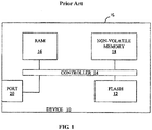
- FIG. 1 is a high level schematic block diagram of a conventional NAND flash media device in a non-volatile data storage unit.
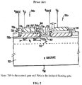
- FIG. 2 shows a cross sectional view of a conventional flash memory device.
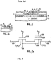
- FIG. 3 An example of a conventional multiple level (MLC) flash memory cell is illustrated in FIG. 3 , where a split channel device has two different threshold voltages, Vt1 and Vt2.
- MLC multiple level flash memory cell
- FIG. 4 depicts the threshold voltage spans in a conventional two-bit MLC device.
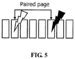
- Pages of data sharing the same multiple level cells are called "shared pages". Each manufacturer may use a different distance between its shared pages. Many memory vendors prefer to set the distance at four. For example, at a pair distance of 4, page 0 is paired with page 4, page 1 is paired with page 5, page 2 is paired with page 6, and page 3 is paired with page 7.
- FIG. 5 shows the paired pages concept at the pair distance of 4.
- the paired pages may share the same memory cells in a MLC flash memory system (e.g., in a 2-bit MLC flash memory, bit 0 and bit 1 of a memory cell are bits from the first and second pages of the paired pages, respectively).
- a program operation is abnormally aborted, for example, during a power down or a reset, not only is the page data that is being programmed damaged, the data in the paired page may also be damaged, even though it may have been written correctly at a previous time.
- RAID techniques are applied in a method along two dimensions.
- the method preserves parity information on the same page.
- the first dimensional RAID uses row parity or the sector parity, which is calculated using data from the first sector to the last sector in the same page.
- FIG. 7 there are 31 sectors of data in each page, respectively labeled Sec 00 to Sec 30.
- a single sector within each page is reserved for storing the first dimensional RAID data (i.e., the row or sector parity).
- p0 sector is the parity sector for Page 0
- sector pX is the parity sector for Page X.
- ECC error correction code
- parity data in the parity sector allows recovery of any sector in a page within the ECC capability of the sector, in the event of a power interruption.
- Sector parity may be calculated from all the data in the page at the time the data is moved from the controller to a chip buffer.
- the method preserves parity data calculated over a number of pages in a parity group.
- parity data is referred to as group parity.
- the number of pages in each parity group is variable. In one implementation, for example, the number of pages in a parity group is 8 pages.
- FIG. 6 illustrates column parity in a 64 page data set.
- each column parity value is calculated over the same sectors, for example, Sec X, from all the pages.
- the parity value is calculated and written in a parity page designated for the block, with a column parity calculated for the same sector in all the pages of the block.
- Group parity in the second dimensional RAID provides additional parity protection in a flash memory device.
- a group parity for a parity group that includes less than all pages of a block sets a higher level of protection than column parity which is illustrated in FIG. 6 .
- the number of pages in the parity group is selected as the group size. This number is chosen carefully in order to provide adequate protection from paired page faults and is often selected by the MLC flash memory manufacturer. For the pairing chosen, a typical group size is 8.
- FIG. 8 shows group parity with 8 pages in each parity sector group. In FIG. 8 , pages p3, p11, ..., p59 are parity pages.
- Figure 10 illustrates a parity grouping configuration applicable to the configuration shown in FIG. 8 , according to one embodiment of the present invention.
- the first group i.e., Group 1
- the first 4 pages are paired with the 4 pages in the previous group.
- the page pairing sequence at the multiple level cells is 0-4, 1-5, 2-6 and 3-7 (i.e. page 0 is paired to page 4, page 1 is paired to page 5, page 2 is paired to page 6, and page 3 is paired to page 7)
- page 0 is paired to page 4
- page 1 is paired to page 5
- page 2 is paired to page 6
- page 3 is paired to page 7
- FIG. 9 is a table that summarizes the 2-dimensional RAID group parity scheme showing a flash memory data set of 63 pages (rows) and 31 sectors (columns). As shown in FIG. 9 , Page 3, Page 11 ... and Page 59 are such selected to be the group parity pages for 8-page groups. First half of each group is paired, or co-resided with the second half of the previous group, on the same MLC flash memory device.
- FIG. 11 illustrates a parity grouping configuration in another embodiment of the present invention.
- all groups contain 8 pages.
- the page pairing sequence at the multiple level cells is 0-4, 1-5, 2-6 and 3-7 (i.e. page 0 is paired to page 4, page 1 is paired to page 5, page 2 is paired to page 6, and page 3 is paired to page 7).
- the group parity for pages 0-3 is written to a set-aside parity page in parity block outside the data pages. If there is power interruption during a subsequent writing of any of pages 4-7, the parity page in the set-aside parity block may be used to recover the damaged data in pages 0-3. If pages 4-7 are written successfully, the parity page for pages 0-3 in the parity block outside the data pages can be saved for future reference, and also can be erased if desirable. This process is repeated for every 8 pages.
- RAID protection does not require reads to generate the parity data on writes. All that is required is a parity cache for the pages being written. This simplifies the algorithm required for parity generation and does not cause a write performance penalty. The only time performance is affected is during the rebuild of data in the event that a hard error is encountered.
- each of the 64 pages is provided with a parity sector (located, for example, in the second sector of each page).
- the parity sector in each page provides the first dimensional RAID.
- each sector stores the column parity calculated based on all the corresponding sectors of all the pages.
- the group parity may be written to set-aside parity blocks. Alternatively, the group parity may use the 4 th , 11 th , 19 th ... 59 th pages to store group parity pages along with the data pages.
- the set-aside parity blocks after the second half group of the paired pages are written without any power interruptions, the set-aside parity block written for the first half of the paired pages may be erased or may be saved for future reference.
- FIG. 12 illustrates how the two dimensional RAID protection works when a number of uncorrectable sectors occur in one embodiment of the present invention (the corrupted sectors are represented in FIG. 12 by densely lined blocks).
- Sec 00 in Page 4 and Sec 02 in Page 5 are single errors in the respective pages; therefore, the data loss in the corresponding sector can be recovered from the parity sector on each of those pages respectively.
- Page 7 is corrupted in two sectors
- the corruption in Sec 00 in Page 7 can be recovered from the group parity page 11.
- the corruption in Sec 02 in Page 9 can also be recovered from the group parity page 11.
- both Sec 30 in Page 7 and Sec 30 in Page 9 can be recovered from the parity sectors p7 and p9 respectively, since the other sectors in those pages have been recovered. Thus it is possible to recover data even though there are two bad sectors in one page or in one column.
- the group sector parity is able to recover corrupted data by combining the row parity, column parity and group parity.
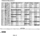
- One example of the recovery scheme is illustrated in FIG. 13 , where multiple hard errors exist (the error sectors are represented with dense-lined blocks).
- Sec 00 in Page 0, Sec 02 in Page 1 and Sec 02 in Page 5 are single errors in the corresponding pages; therefore, they can be recovered from the parity sectors in those pages respectively.
- Sec 29 in Page 9 can be recovered from the group parity in Sec 29 of Page 11.
- Sec 00 in Page 3 can be recovered by recalculating group parity of Sec 00 over pages 0-2, and Sec 02 in Page 9 can be recovered from the group parity of Sec 02 in Page 11. Subsequent to those corrections, Sec 00 in Page 7 is correctable from the group parity page 11, Sec 02 in Page 13, and Sec 29 in Page 13 can be recovered from the group parity page 19. Following the above corrections, Sec 30 in Page 3, Sec 30 in Page 7, Sec 30 in Page 9 and Sec 30 in Page 13 can be recovered from the corresponding parity sectors since the other bad sectors in relevant pages have been recovered. Thus it is possible to recover data even though there are four sectors with hard errors residing in one column.
- an algorithm can be written for the process of data writing, when data is protected against the write-corrupt at a power interruption.
- This algorithm comprises the following steps for a parity group of 8 pages:
- This algorithm is also illustrated in FIG. 14 .
Description
- The invention described herein relates to data storage management in semiconductor flash memories, and in particular to a data storage protection method that prevents data corruption in multiple level cell (MLC) memory devices in the event of a power interruption.
- Current enterprise-level mass storage relies on hard drives that are typically characterized by a 3.5" form factor, a 15,000 rpm spindle motor and a storage capacity between 73GB and 450GB. The mechanical design follows the traditional hard drive with a single actuator and 8 read/write heads moving across 8 surfaces. The constraints of the head/media technology limit the read/write capabilities to using only one active head at a time. All data requests that are sent to the drive are handled in a serial manner, with long delays between operations, as the actuator moves the read/write head to the required position and the media rotates to place the data under the read/write head.
- A solid state memory device is attractive in an enterprise mass-storage environment. For that environment, the flash memory is a good candidate among various solid state memory devices, since it does not have the mechanical delays
associated with hard drives, thereby allowing higher performance and commensurately lower cost, and better usage of power and space. - The flash memory is a form of non-volatile memory, i.e. EEPROM (electronically erasable programmable read-only memory). A memory cell in a flash memory array generally includes a transistor having a control gate and drain and source diffusion regions formed in a substrate. The transistor has a floating gate under the control gate, thus forming an electron storage device. A channel region lies under the floating gate, isolated by an insulation layer (e.g. a tunnel oxide layer) between the channel and the floating gate. The energy barrier imposed by the insulating layer against charge carriers movement into or out of the floating gate can be overcome by applying a sufficiently high electric field across the insulating layer. The charge stored in the floating gate determines the threshold voltage (Vt) of the cell, which represents the stored data of the cell. Charge stored in the floating gate causes the cell to have a higher Vt. To change the Vt of a cell to a higher or lower value, the charge stored in the floating gate is increased or decreased by applying appropriate voltages at the control gate, the drain and source diffusion regions, and the channel region. The appropriate voltages cause charge to move between one or more of these regions and through the insulation layer to the floating gate.
- A single-level cell (SLC) flash memory device has a single threshold voltage Vt and can store one bit of data per cell. A memory cell in a multiple-level cell (MLC) flash memory device has multiple threshold voltages, and depending on the amount of charge stored in the floating gate, can represent more than one bit of data. Because a MLC flash memory device enables the storage of multiple data bits per cell, high density mass storage applications (such as 512 Mb and beyond) are readily achievable. In a typical four-level two-bit MLC flash memory device, the cell threshold voltage Vt can be set at any of four levels to represent data "00", "01", "10", and "11". To program the memory cell to a given level, the cell may be programmed multiple times. Before each write, a flash memory array is erased to reset every cell in the array to a default state. As a result, multiple data bits that share the same cell and their electronic states, (hence their threshold voltage Vt's), are interdependent to a point that an unexpected power interruption can generate unpredictable consequences. Variations in the electronic states of the memory cells also generate variations within ranges of threshold voltages in a real system. Table 1 below shows the electronic states and the threshold voltage ranges in a two-bit MLC.
Table 1 Threshold voltages and bit values in a two-bit MLC memory cell Vt Bit 1 Bit 2 -4.25V to -1.75 V 1 1 -1.75V to 0.75 V 1 0 0.75V to 3.25 V 0 1 3.25V to 5.75 V 0 0 - In spite of the advantages of MLC over SLC, MLC flash memory devices have not traditionally been used because of certain technical constraints, among which data corruption presents one of the most severe challenges.
- All flash memories have a finite number of erase-write cycles. MLC flash memory devices are more vulnerable to data corruption than SLC flash memory devices. The specified erase cycle limit for each flash memory page is typically in the order of 100,000 cycles for SLC flash memory devices and typically in the order of 10,000 cycles for MLC devices. The lower cycle limit in the MLC flash memory devices poses particular problems for data centers that operate with unpredictable data streams. The unpredictable data streams may cause "hot spots", resulting in certain highly-used areas of memory being subject to a large number of erase cycles.
- In addition, various factors in normal operation can also affect flash memory integrity, including read disturbs or program disturbs. These disturbs lead to unpredictable loss of data bits in a memory cell, as a result of the reading or writing of memory cells adjacent to the disturbed cell. Sudden data losses in MLC flash memory devices due to unexpected power interruptions require frequent data recoveries. Because some data levels require more than one write operations to achieve and because more than one bit of data share the same memory cell, a power change or a program error during a write data operation leaves the data in a wrong state. When the power returns, the memory cell can be in an erratic state. Therefore a power interruption is a major risk to the integrity of data stored in MLC flash memory devices.
- Flash media typically are written in units called "pages"; each page typically includes between 2000 bytes and 8000 bytes. Flash media typically are erased in units called "blocks". Each block typically includes between 16 and 64 pages. Pages in MLC flash memory devices are coupled into paired pages. The number of paired pages maybe two for the 2-bit MLC and may go up to 3 to 4 or higher for higher bit MLCs. The paired pages may reside in shared MLC flash memory cells. If the power failure occurs while the MLC is in the middle of an operation that changes the contents of the flash media (e.g., in the middle of writing a page of data or in the middle of erasing a block of data), the electrical states of the interrupted page or block are unpredictable after the device is powered up again. The electrical states can even be random, because some of the affected bits may already be in the states assigned to them by the operation, at the time power is interrupted. However, other bits may be lagging behind and have not yet reached their target values yet. Furthermore, some bits might be caught in intermediate states and thus be in an unreliable mode, so that reading these bits returns different results under different read operations. Therefore power losses while programming a certain page can corrupt a paired page.
- In the prior arts, error correction codes (ECC) and Redundant Array of Inexpensive Disk (RAID) techniques have been used to mitigate data corruption. In one instance, data corruption is prevented by writing parity pages at a different page address. Those techniques require either additional memory or complicated error-searching and data rebuilding procedures after power returns. Such requirements or solutions make the process costly to implement and place significant strain on the processing power of a conventional flash memory controller, which generally includes only a single processor. Furthermore, if a power failure occurs during the writing of a page, the paired page data can become corrupt in a MLC flash memory device. Therefore even the conventional paired page technique is susceptible to a sudden power interruption. As a matter of fact, the severity of the possible corruption is high; in some cases, every 10th data bit can be lost. Relying on conventional ECC techniques to make a MLC flash memory system reliable would be impractical to implement.
- NAND flash memory data corruption can also result from program erase cycle wear outs. Electrons are injected and removed by tunneling through thin film oxide insulators. Repeated program/erase cycles damage the oxide and reduce its effectiveness. As device dimensions (e.g., oxide film thickness) shrink, data integrity problems from device wearing out can become more severe. One factor that influences this wearing out process is the speed at which the program and erase cycles are performed. However, if the speed of programming and erasing is slowed to avoid wearing out, overall performance can be impacted significantly.
- Currently, a technique exists which applies a lower sense voltage to measure the charge states of the flash memory, in order to extend the lifetime of the memory device. A flash memory device is a charge-trap device that uses sense circuits to detect if a cell contains a given charge level. However, as the device wears out, its ability to store a charge is compromised. A worn out memory device allows the stored charge on the floating gate to leak. Consequently a sense circuit will detect a reduced voltage from the device. One current recovery mechanism reduces the sense voltage that is used to determine the logic value a cell contains. However, a lower sense voltage also returns a lower detected voltage, thus resulting in an incorrect charge tracking.
-
US 2007/150790 discloses a method according to the pre-characterizing portion ofclaim 1. - According to an aspect of the present invention there is provided a method of managing a multiple level cell flash memory that is logically organized to include a block having a plurality of pages. Each page includes a plurality of sectors. The flash memory is erased in units of blocks. The method comprises choosing a parity sector in each page of the plurality of pages in the block, for each page, calculating a sector parity value for data stored in the sectors of the page and storing the sector parity value into the parity sector of the page, assigning the pages of the block into two or more groups and selecting a page in each group as a parity page of the group and, for each respective group of the two or more groups in the block, calculating a group parity value of data stored in the pages of the respective group and storing the group parity value in the parity page of the respective group.
- According to another aspect of the present invention there is provided a multiple level cell flash memory data storage device, comprising a flash memory array having a plurality of blocks. Each block forms an erase unit and having a plurality of pages. A respective block includes a plurality of groups of pages. Each group of pages includes an assigned parity page. Each page of a respective block has a plurality of sectors, including an assigned parity sector. The device is operable, for a respective page, to store data in data sectors of the respective page and to store, in the assigned parity sector of the respective page, a sector parity value of data stored in sectors of the respective page. The device is operable, for each respective group of pages of the plurality of groups of pages in the block, to store data in data pages of the respective group of pages and to store, in the parity page of the respective group, a group parity value of the data stored in the data pages of the respective group.
- The embodiments of the present invention provide a two-dimensional self-RAID method of protecting, following a power loss, page-based storage data in a multiple-level-cell flash memory device. The process includes reserving a parity sector in each data page under an application of RAID ("First dimensional RAID") technique, thereby forming a parity group containing a predetermined number of pages, and repeating the parity grouping for every subsequent data pages under a second application of a RAID technique ("Second dimensional RAID"). Thus if a subsequent write corrupts a paired page, the lost data can be recovered using the two dimensional RAID data.
- The first dimensional parity in the embodiments is associated with a data page. One sector within the page is reserved for the first dimensional RAID data. This parity sector allows the recovery of any single sector within the ECC capability of that sector. This level of RAID data can be calculated from the available data at the time the controller transfers the data to a chip buffer.
- The second dimensional parity in the embodiments is calculated across a column of sectors in a predetermined number of pages. When the specific page number is selected carefully, paired page faults can be recovered.
- Full data protection against power interruption is achieved because any corrupted data sector can be recovered by the RAID data either from the within page sector parity or from the crossed sector page parity.
- The embodiments provide a method of preserving page-based flash memory integrity during writing, in the event of a power loss. The embodiment can be used to manage a flash memory having multiple level cells (MLC).
- According to an embodiment of the present invention, a method is provided to protect a MLC flash memory data which includes numerous memory
pages. A method of managing a multiple level cell flash memory that includes a plurality of pages, each page including a plurality of sequentially numbered sectors, the method comprising: (a) choosing a sector in each page as a parity sector; (b) writing data into each page and calculating a parity value of the sectors in each page and storing the parity value in the reserved parity sectors; (c) dividing data pages into a plurality of groups, wherein each group, except the first group and the last group, consists of a first predetermined number of pages; (d) reserving a page in each group as a group parity page and writing data into each page of the group, calculating a parity value of the group and storing the parity value in the reserved group parity page; (e) repeating (a) to (d) for each group; (f) reserving a new page to store a column parity of all sectors sharing the same sector number. - According to another embodiment of the present invention, a method is provided to protect a MLC flash memory data which includes numerous memory pages. A method of managing a multiple level cell flash memory that includes a plurality of pages, each page including a plurality of sequentially numbered sectors, the method comprising: (a) reserving a parity block; (b) choosing a sector in each page as a parity sector; (c) writing data into each page and calculating a parity value of the sectors in each page and storing the parity value in the chosen parity sector; (d) dividing data pages into a plurality of groups, wherein each group, except the last group, consists of a second predetermined number of pages; (e) writing data into pages in a subset of a group and calculating the subset group parity; (f) storing the subset group parity value in the reserved parity block; (g) writing data into the remaining pages of the group; (h) repeating (b) to (g); (I) reserving a new page to store a column parity of sectors sharing the same sector number but residing in different pages.
- Also discloses is a data storage system in which the above methods can be operated upon.
- Further disclosed is a method for reducing data corruption from device wearing out is provided by extending the programming and erasing time on selected weak cells. Weak cells are identified by the rate they generate errors, and then the blocks and pages associated with the weak cells can be programmed and erased at a slower rate than other cells. By tracking the weaker blocks and treating them differently than other more robust blocks, endurance can be enhanced. Because the slower programming and erasure processes are only performed on the relatively few weak blocks, overall performance is not significantly compromised. A method of managing a multiple level cell flash memory with numerous pages, the method comprising: (a) programming and erasing data on a page at a predetermined speed; (b) detecting an error rate for each of the pages and identifying the pages associated with error rates that exceed a predetermined value; (c) programming and erasing the identified high error page set a speed that is slower than the predetermined speed.
- Also disclosed is a method for overcoming the leakage induced charge level shifts is provided. A method of managing a multiple level cell flash memory that includes a sense circuitry, the method comprising: (a) selecting a sense voltage; (b) detecting charge levels of memory cells in the multiple level cell flash memory with the selected sense
voltage, and making a first table that correlates the predetermined sense voltage and the sensed charge levels; (c) reducing the sense voltage and detecting charge levels of memory cells in the multiple level cell flash memory using the reduced sense voltage and making a second table that correlates the reduced sensed voltage with the sensed charge levels; (d) replacing the first table with the second table. - The present invention is better understood upon consideration of the detailed description below in conjunction with the accompanying drawings.
-
-
FIG. 1 shows a schematic block diagram of a device controller using a flash medium for non-volatile data storage. -
FIG. 2 is a cross sectional view of a flash memory device. -
FIG. 3 shows a cross sectional view of a multi-level flash memory cell and its equivalent circuit diagram. -
FIG. 4 shows a two bit-MLC threshold voltage ranges in a MLC flash memory device. -
FIG. 5 is a flash memory paired page diagram. -
FIG. 6 illustrates the concept of column parity without group parity. -
FIG. 7 illustrates the concept of sector parity or row parity. -
FIG. 8 shows group parity with 8 pages in each parity sector group. -
FIG. 9 is a table that summarizes the 2-dimensional RAID group parity scheme showing a flash memory data set of 63 pages (rows) and 31 sectors (columns). -
FIG. 10 shows 8-page group parity configuration in accordance with an embodiment of the present invention. -
FIG. 11 shows 8-page group parity configuration using a set aside parity block in accordance with another embodiment of the present invention. -
FIG. 12 shows a protection scheme using a two-dimensional RAID technique (example 1). -
FIG. 13 shows a protection scheme using a two-dimensional RAID technique (example 2). -
FIG. 14 is a flow chart of an algorithm which protects a MLC flash memory device against corruption resulting from a power interruption during a write operation. -
FIG. 1 is a high level schematic block diagram of a conventional NAND flash media device in a non-volatile data storage unit. -
FIG. 2 shows a cross sectional view of a conventional flash memory device. - An example of a conventional multiple level (MLC) flash memory cell is illustrated in
FIG. 3 , where a split channel device has two different threshold voltages, Vt1 and Vt2. The referenced cross sectional view and equivalent circuit are taken fromUS Pat. 5,045,940 (Harari ). - Variations of the electronic states generate ranges of threshold voltages in a real MLC system.
FIG. 4 depicts the threshold voltage spans in a conventional two-bit MLC device. - Pages of data sharing the same multiple level cells are called "shared pages". Each manufacturer may use a different distance between its shared pages. Many memory vendors prefer to set the distance at four. For example, at a pair distance of 4,
page 0 is paired withpage 4,page 1 is paired withpage 5,page 2 is paired withpage 6, andpage 3 is paired withpage 7.FIG. 5 shows the paired pages concept at the pair distance of 4. - The paired pages may share the same memory cells in a MLC flash memory system (e.g., in a 2-bit MLC flash memory,
bit 0 andbit 1 of a memory cell are bits from the first and second pages of the paired pages, respectively). When a program operation is abnormally aborted, for example, during a power down or a reset, not only is the page data that is being programmed damaged, the data in the paired page may also be damaged, even though it may have been written correctly at a previous time. - According to one embodiment of the present invention, RAID techniques are applied in a method along two dimensions. In the first dimension, "the first dimensional RAID"), the method preserves parity information on the same page. The first dimensional RAID uses row parity or the sector parity, which is calculated using data from the first sector to the last sector in the same page. As shown in
FIG. 7 , there are 31 sectors of data in each page, respectively labeledSec 00 toSec 30. A single sector within each page is reserved for storing the first dimensional RAID data (i.e., the row or sector parity). InFig. 7 , p0 sector is the parity sector forPage 0, and sector pX is the parity sector for Page X. One common error correction code (ECC) allows single-bit error correction. With an extra parity bit, double-bit errors can be detected. Therefore the parity data in the parity sector allows recovery of any sector in a page within the ECC capability of the sector, in the event of a power interruption. Sector parity may be calculated from all the data in the page at the time the data is moved from the controller to a chip buffer. - In the second dimension ("the second dimensional RAID"), the method preserves parity data calculated over a number of pages in a parity group. Such parity data is referred to as group parity. The number of pages in each parity group is variable. In one implementation, for example, the number of pages in a parity group is 8 pages.
- Group parity that is calculated for corresponding sectors over all pages in a block is referred to column parity.
FIG. 6 illustrates column parity in a 64 page data set. InFIG. 6 , each column parity value is calculated over the same sectors, for example, Sec X, from all the pages. The parity value is calculated and written in a parity page designated for the block, with a column parity calculated for the same sector in all the pages of the block. - Group parity in the second dimensional RAID provides additional parity protection in a flash memory device. A group parity for a parity group that includes less than all pages of a block sets a higher level of protection than column parity which is illustrated in
FIG. 6 . As a first step, the number of pages in the parity group is selected as the group size. This number is chosen carefully in order to provide adequate protection from paired page faults and is often selected by the MLC flash memory manufacturer. For the pairing chosen, a typical group size is 8.FIG. 8 shows group parity with 8 pages in each parity sector group. InFIG. 8 , pages p3, p11, ..., p59 are parity pages. -
Figure 10 illustrates a parity grouping configuration applicable to the configuration shown inFIG. 8 , according to one embodiment of the present invention. As shown inFIG. 10 , the first group (i.e., Group 1) is a half group. In each subsequent group of 8 pages, the first 4 pages are paired with the 4 pages in the previous group. For instance, if the page pairing sequence at the multiple level cells is 0-4, 1-5, 2-6 and 3-7 (i.e.page 0 is paired topage 4,page 1 is paired topage 5,page 2 is paired topage 6, andpage 3 is paired to page 7), then for each write of any ofpages group parity page 3. In the event that a subsequent write of a page in any ofpages 4 to 6 corrupts the corresponding pairedpage group parity page 3. Thus the group parity page protects page 0-2 inparity group 1 of 4 pages. Thegroup 2 parity page ispage 11, protectingpage pages 12 to 14.FIG. 9 is a table that summarizes the 2-dimensional RAID group parity scheme showing a flash memory data set of 63 pages (rows) and 31 sectors (columns). As shown inFIG. 9 ,Page 3,Page 11 ... andPage 59 are such selected to be the group parity pages for 8-page groups. First half of each group is paired, or co-resided with the second half of the previous group, on the same MLC flash memory device. -
FIG. 11 illustrates a parity grouping configuration in another embodiment of the present invention. InFIG. 11 , all groups contain 8 pages. The page pairing sequence at the multiple level cells is 0-4, 1-5, 2-6 and 3-7 (i.e.page 0 is paired topage 4,page 1 is paired topage 5,page 2 is paired topage 6, andpage 3 is
paired to page 7). The group parity for pages 0-3 is written to a set-aside parity page in parity block outside the data pages. If there is power interruption during a subsequent writing of any of pages 4-7, the parity page in the set-aside parity block may be used to recover the damaged data in pages 0-3. If pages 4-7 are written successfully, the parity page for pages 0-3 in the parity block outside the data pages can be saved for future reference, and also can be erased if desirable. This process is repeated for every 8 pages. - Another advantage of this type of RAID protection is that it does not require reads to generate the parity data on writes. All that is required is a parity cache for the pages being written. This simplifies the algorithm required for parity generation and does not cause a write performance penalty. The only time performance is affected is during the rebuild of data in the event that a hard error is encountered.
- Although in the detailed description of the current invention, an exemplary number of 8 are used as the number of pages in a group, the invention does not limit the number of pages in a group to 8.
- To implement the scheme shown in
FIG. 11 , in the first dimension, each of the 64 pages is provided with a parity sector (located, for example, in the second sector of each page). The parity sector in each page provides the first dimensional RAID. In the second dimension, there are two levels of parity protection. First, there is column parity for all pages. In the column parity page, each sector stores the column parity calculated based on all the corresponding sectors of all the pages. Second, group parity is also recorded according for pages grouped according to a selected group size. The group parity may be written to set-aside parity blocks. Alternatively, the group parity may use the 4th, 11th, 19th ... 59th pages to store group parity pages along with the data pages. In one embodiment using set-aside parity blocks, after the second half group of the paired pages are written without any power interruptions, the set-aside parity block written for the first half of the paired pages may be erased or may be saved for future reference. -
FIG. 12 illustrates how the two dimensional RAID protection works when a number of uncorrectable sectors occur in one embodiment of the present invention (the corrupted sectors are represented inFIG. 12 by densely lined blocks). For example,Sec 00 inPage 4 andSec 02 inPage 5 are single errors in the respective pages; therefore, the data loss in the corresponding sector can be recovered from the parity sector on each of those pages respectively. However, asPage 7 is corrupted in two sectors, the corruption inSec 00 inPage 7 can be recovered from thegroup parity page 11. Similarly, the corruption inSec 02 inPage 9 can also be recovered from thegroup parity page 11. Subsequent to the above corrections, bothSec 30 inPage 7 andSec 30 inPage 9 can be recovered from the parity sectors p7 and p9 respectively, since the other sectors in those pages have been recovered. Thus it is possible to recover data even though there are two bad sectors in one page or in one column. - In a more severe power interruption scenario when a number of paired pages are affected in a single page or in a single column, the group sector parity is able to recover corrupted data by combining the row parity, column parity and group parity. One example of the recovery scheme is illustrated in
FIG. 13 , where multiple hard errors exist (the error sectors are represented with dense-lined blocks).Sec 00 inPage 0,Sec 02 inPage 1 andSec 02 inPage 5 are single errors in the corresponding pages; therefore, they can be recovered from the parity sectors in those pages respectively.Sec 29 inPage 9 can be recovered from the group parity inSec 29 ofPage 11. After these corrections are made,Sec 00 inPage 3 can be recovered by recalculating group parity ofSec 00 over pages 0-2, andSec 02 inPage 9 can be recovered from the group parity ofSec 02 inPage 11. Subsequent to those corrections,Sec 00 inPage 7 is correctable from thegroup parity page 11,Sec 02 inPage 13, andSec 29 inPage 13 can be recovered from the group parity page 19. Following the above corrections,Sec 30 inPage 3,Sec 30 inPage 7,Sec 30 inPage 9 andSec 30 inPage 13 can be recovered from the corresponding parity sectors since the other bad sectors in relevant pages have been recovered. Thus it is possible to recover data even though there are four sectors with hard errors residing in one column. - In one embodiment of the present invention where a set aside parity block outside the data pages is used to reserve the group parity, an algorithm can be written for the process of data writing, when data is protected against the write-corrupt at a power interruption. This algorithm comprises the following steps for a parity group of 8 pages:
- a. Write 4 pages from
pages 0 topage 3 and calculate the group parity for pages 0-3; - b. Write the group parity page to a Parity-Block outside the data memory;
- c. Write pages 4-7;
- d. Release the Parity-Block of pages 0-3, used Parity-Block can be saved or erased;
- e. Repeat the process a) to d) for every subsequent group of 8 pages;
- f. Treat the last group the same way even if the last group has less than 8 pages.
- This algorithm is also illustrated in
FIG. 14 . - The foregoing description is intended to illustrate, but not to limit, the scope of the invention, which is defined by the scope of the appended claims. Other embodiments are within the scope of this disclosure.
Claims (13)
- A method of managing a multiple level cell flash memory (12) that is logically organized to include a block having a plurality of pages, each page including a plurality of sectors, wherein the flash memory is erased in units of blocks, the method comprising:choosing a parity sector in each page of the plurality of pages in the block;for each page, calculating a sector parity value for data stored in the sectors of the page and storing the sector parity value into the parity sector of the page;CHARACTERISED BY:assigning the pages of the block into two or more groups and selecting a page in each group as a parity page of the group; andfor each respective group of the two or more groups in the block, calculating a group parity value of data stored in the pages of the respective group and storing the group parity value in the parity page of the respective group.
- The method of managing flash memory as in claim 1, wherein the sectors of each page are each assigned a sector number, the method further comprising:selecting a column parity page for the block and calculating, for each sector number, a column parity for all sectors of the sector number in the pages of the block.
- The method of claim 1 or 2, wherein each group consists of 8 pages.
- The method of claim 1 or 2, wherein each multiple level cell is shared by at least two pages of the block.
- The method as in claim 4, wherein the pages sharing a respective multiple level cell are assigned to different groups.
- The method as in claim 5, wherein the groups are each assigned a group number and wherein the pages sharing the respective multiple level cell are assigned consecutive group numbers.
- The method as in claim 6, wherein one or more of the groups are assigned half the number of pages as assigned to each of the remainder of the groups of the block.
- A multiple level cell flash memory data storage device (15), comprising:a flash memory array (12) having a plurality of blocks, each block forming an erase unit and having a plurality of pages, a respective block including a plurality of groups of pages, each group of pages including an assigned parity page;each page of the respective block having a plurality of sectors, including an assigned parity sector;wherein the device is operable to, for a respective page,to store data in data sectors of the respective page;to store, in the assigned parity sector of the respective page, a sector parity value of data stored in sectors of the respective page; andwherein the device is operable, for each respective group of pages of the plurality of groups of pages in the block,to store data in data pages of the respective group of pages;to store, in the parity page of the respective group, a group parity value of the data stored in the data pages of the respective group.
- The multiple level cell flash memory data storage device of claim 8, wherein the sectors of each page are each assigned a sector number, and the device is operable, for the respective group of pages, to select a column parity page for the block and to calculate, for each sector number, a column parity for all sectors of the sector number in the pages of the block.
- The multiple level cell flash memory data storage device of claim 8 or 9, wherein each group consists of 8 pages.
- The multiple level cell flash memory data storage device of claim 8 or 9, wherein each multiple level cell of the multiple level cell flash memory device is shared by at least two pages of the block.
- The multiple level cell flash memory data storage device of claim 11, wherein the pages sharing a respective multiple level cell are assigned to different groups.
- The multiple level cell flash memory data storage device of claim 12, wherein the groups are each assigned a group number and wherein the pages sharing the respective multiple level cell are assigned consecutive group numbers.
Applications Claiming Priority (2)
| Application Number | Priority Date | Filing Date | Title |
|---|---|---|---|
| US12/726,200 US8365041B2 (en) | 2010-03-17 | 2010-03-17 | MLC self-raid flash data protection scheme |
| PCT/US2011/028637 WO2011116071A2 (en) | 2010-03-17 | 2011-03-16 | Mlc self-raid flash data protection scheme |
Publications (3)
| Publication Number | Publication Date |
|---|---|
| EP2548121A2 EP2548121A2 (en) | 2013-01-23 |
| EP2548121A4 EP2548121A4 (en) | 2015-11-18 |
| EP2548121B1 true EP2548121B1 (en) | 2017-11-29 |
Family
ID=44647151
Family Applications (1)
| Application Number | Title | Priority Date | Filing Date |
|---|---|---|---|
| EP11756916.0A Active EP2548121B1 (en) | 2010-03-17 | 2011-03-16 | Mlc self-raid flash data protection scheme |
Country Status (6)
| Country | Link |
|---|---|
| US (4) | US8365041B2 (en) |
| EP (1) | EP2548121B1 (en) |
| JP (1) | JP2013522776A (en) |
| KR (1) | KR101795093B1 (en) |
| CN (1) | CN102906712B (en) |
| WO (1) | WO2011116071A2 (en) |
Families Citing this family (187)
| Publication number | Priority date | Publication date | Assignee | Title |
|---|---|---|---|---|
| US7934052B2 (en) | 2007-12-27 | 2011-04-26 | Pliant Technology, Inc. | System and method for performing host initiated mass storage commands using a hierarchy of data structures |
| US8365041B2 (en) | 2010-03-17 | 2013-01-29 | Sandisk Enterprise Ip Llc | MLC self-raid flash data protection scheme |
| US8417877B2 (en) * | 2010-08-31 | 2013-04-09 | Micron Technology, Inc | Stripe-based non-volatile multilevel memory operation |
| US8909982B2 (en) | 2011-06-19 | 2014-12-09 | Sandisk Enterprise Ip Llc | System and method for detecting copyback programming problems |
| US8910020B2 (en) | 2011-06-19 | 2014-12-09 | Sandisk Enterprise Ip Llc | Intelligent bit recovery for flash memory |
| US8589640B2 (en) | 2011-10-14 | 2013-11-19 | Pure Storage, Inc. | Method for maintaining multiple fingerprint tables in a deduplicating storage system |
| US9058289B2 (en) | 2011-11-07 | 2015-06-16 | Sandisk Enterprise Ip Llc | Soft information generation for memory systems |
| US9053809B2 (en) * | 2011-11-09 | 2015-06-09 | Apple Inc. | Data protection from write failures in nonvolatile memory |
| US8954822B2 (en) | 2011-11-18 | 2015-02-10 | Sandisk Enterprise Ip Llc | Data encoder and decoder using memory-specific parity-check matrix |
| US8924815B2 (en) | 2011-11-18 | 2014-12-30 | Sandisk Enterprise Ip Llc | Systems, methods and devices for decoding codewords having multiple parity segments |
| US9048876B2 (en) | 2011-11-18 | 2015-06-02 | Sandisk Enterprise Ip Llc | Systems, methods and devices for multi-tiered error correction |
| US20130173972A1 (en) * | 2011-12-28 | 2013-07-04 | Robert Kubo | System and method for solid state disk flash plane failure detection |
| CN102609370B (en) * | 2012-02-06 | 2014-12-17 | 记忆科技(深圳)有限公司 | Solid-state disk and method for preventing data loss thereof |
| US8923045B2 (en) | 2012-05-31 | 2014-12-30 | Seagate Technology Llc | Multi-level cell (MLC) update with protected mode capability |
| US9699263B1 (en) | 2012-08-17 | 2017-07-04 | Sandisk Technologies Llc. | Automatic read and write acceleration of data accessed by virtual machines |
| US9298383B2 (en) * | 2012-08-17 | 2016-03-29 | International Business Machines Corporation | Memory with mixed cell array and system including the memory |
| US8887011B2 (en) * | 2012-09-13 | 2014-11-11 | Sandisk Technologies Inc. | Erased page confirmation in multilevel memory |
| US9047974B2 (en) | 2012-10-04 | 2015-06-02 | Sandisk Technologies Inc. | Erased state reading |
| US8464095B1 (en) * | 2012-11-15 | 2013-06-11 | DSSD, Inc. | Method and system for multi-dimensional raid reconstruction and defect avoidance |
| US9501398B2 (en) | 2012-12-26 | 2016-11-22 | Sandisk Technologies Llc | Persistent storage device with NVRAM for staging writes |
| US9612948B2 (en) | 2012-12-27 | 2017-04-04 | Sandisk Technologies Llc | Reads and writes between a contiguous data block and noncontiguous sets of logical address blocks in a persistent storage device |
| US9239751B1 (en) | 2012-12-27 | 2016-01-19 | Sandisk Enterprise Ip Llc | Compressing data from multiple reads for error control management in memory systems |
| CN103092765B (en) * | 2012-12-31 | 2015-08-05 | 记忆科技(深圳)有限公司 | Solid-state memory system, device and method for writing data |
| US9454420B1 (en) | 2012-12-31 | 2016-09-27 | Sandisk Technologies Llc | Method and system of reading threshold voltage equalization |
| US9003264B1 (en) | 2012-12-31 | 2015-04-07 | Sandisk Enterprise Ip Llc | Systems, methods, and devices for multi-dimensional flash RAID data protection |
| US9214965B2 (en) | 2013-02-20 | 2015-12-15 | Sandisk Enterprise Ip Llc | Method and system for improving data integrity in non-volatile storage |
| US9329928B2 (en) | 2013-02-20 | 2016-05-03 | Sandisk Enterprise IP LLC. | Bandwidth optimization in a non-volatile memory system |
| US9870830B1 (en) | 2013-03-14 | 2018-01-16 | Sandisk Technologies Llc | Optimal multilevel sensing for reading data from a storage medium |
| US9236886B1 (en) | 2013-03-15 | 2016-01-12 | Sandisk Enterprise Ip Llc | Universal and reconfigurable QC-LDPC encoder |
| US9009576B1 (en) | 2013-03-15 | 2015-04-14 | Sandisk Enterprise Ip Llc | Adaptive LLR based on syndrome weight |
| US9136877B1 (en) | 2013-03-15 | 2015-09-15 | Sandisk Enterprise Ip Llc | Syndrome layered decoding for LDPC codes |
| US9244763B1 (en) | 2013-03-15 | 2016-01-26 | Sandisk Enterprise Ip Llc | System and method for updating a reading threshold voltage based on symbol transition information |
| US9367246B2 (en) | 2013-03-15 | 2016-06-14 | Sandisk Technologies Inc. | Performance optimization of data transfer for soft information generation |
| US9092350B1 (en) | 2013-03-15 | 2015-07-28 | Sandisk Enterprise Ip Llc | Detection and handling of unbalanced errors in interleaved codewords |
| US9170941B2 (en) | 2013-04-05 | 2015-10-27 | Sandisk Enterprises IP LLC | Data hardening in a storage system |
| US10049037B2 (en) | 2013-04-05 | 2018-08-14 | Sandisk Enterprise Ip Llc | Data management in a storage system |
| US9159437B2 (en) | 2013-06-11 | 2015-10-13 | Sandisk Enterprise IP LLC. | Device and method for resolving an LM flag issue |
| US9384126B1 (en) | 2013-07-25 | 2016-07-05 | Sandisk Technologies Inc. | Methods and systems to avoid false negative results in bloom filters implemented in non-volatile data storage systems |
| US9524235B1 (en) | 2013-07-25 | 2016-12-20 | Sandisk Technologies Llc | Local hash value generation in non-volatile data storage systems |
| US9043517B1 (en) | 2013-07-25 | 2015-05-26 | Sandisk Enterprise Ip Llc | Multipass programming in buffers implemented in non-volatile data storage systems |
| US9639463B1 (en) | 2013-08-26 | 2017-05-02 | Sandisk Technologies Llc | Heuristic aware garbage collection scheme in storage systems |
| US9235509B1 (en) | 2013-08-26 | 2016-01-12 | Sandisk Enterprise Ip Llc | Write amplification reduction by delaying read access to data written during garbage collection |
| US9442670B2 (en) | 2013-09-03 | 2016-09-13 | Sandisk Technologies Llc | Method and system for rebalancing data stored in flash memory devices |
| US9519577B2 (en) | 2013-09-03 | 2016-12-13 | Sandisk Technologies Llc | Method and system for migrating data between flash memory devices |
| US9158349B2 (en) | 2013-10-04 | 2015-10-13 | Sandisk Enterprise Ip Llc | System and method for heat dissipation |
| US9323637B2 (en) | 2013-10-07 | 2016-04-26 | Sandisk Enterprise Ip Llc | Power sequencing and data hardening architecture |
| US9442662B2 (en) | 2013-10-18 | 2016-09-13 | Sandisk Technologies Llc | Device and method for managing die groups |
| US9298608B2 (en) | 2013-10-18 | 2016-03-29 | Sandisk Enterprise Ip Llc | Biasing for wear leveling in storage systems |
| US9436831B2 (en) | 2013-10-30 | 2016-09-06 | Sandisk Technologies Llc | Secure erase in a memory device |
| US9263156B2 (en) | 2013-11-07 | 2016-02-16 | Sandisk Enterprise Ip Llc | System and method for adjusting trip points within a storage device |
| US9244785B2 (en) | 2013-11-13 | 2016-01-26 | Sandisk Enterprise Ip Llc | Simulated power failure and data hardening |
| US9152555B2 (en) | 2013-11-15 | 2015-10-06 | Sandisk Enterprise IP LLC. | Data management with modular erase in a data storage system |
| US9703816B2 (en) | 2013-11-19 | 2017-07-11 | Sandisk Technologies Llc | Method and system for forward reference logging in a persistent datastore |
| US9520197B2 (en) | 2013-11-22 | 2016-12-13 | Sandisk Technologies Llc | Adaptive erase of a storage device |
| US9520162B2 (en) | 2013-11-27 | 2016-12-13 | Sandisk Technologies Llc | DIMM device controller supervisor |
| US9122636B2 (en) | 2013-11-27 | 2015-09-01 | Sandisk Enterprise Ip Llc | Hard power fail architecture |
| US9280429B2 (en) | 2013-11-27 | 2016-03-08 | Sandisk Enterprise Ip Llc | Power fail latching based on monitoring multiple power supply voltages in a storage device |
| US9250676B2 (en) | 2013-11-29 | 2016-02-02 | Sandisk Enterprise Ip Llc | Power failure architecture and verification |
| US9582058B2 (en) | 2013-11-29 | 2017-02-28 | Sandisk Technologies Llc | Power inrush management of storage devices |
| US9092370B2 (en) | 2013-12-03 | 2015-07-28 | Sandisk Enterprise Ip Llc | Power failure tolerant cryptographic erase |
| US9235245B2 (en) | 2013-12-04 | 2016-01-12 | Sandisk Enterprise Ip Llc | Startup performance and power isolation |
| US9129665B2 (en) | 2013-12-17 | 2015-09-08 | Sandisk Enterprise Ip Llc | Dynamic brownout adjustment in a storage device |
| US9262268B2 (en) * | 2013-12-20 | 2016-02-16 | Seagate Technology Llc | Method to distribute user data and error correction data over different page types by leveraging error rate variations |
| US10417090B2 (en) | 2013-12-23 | 2019-09-17 | Cnex Labs, Inc. | Computing system with data protection mechanism and method of operation thereof |
| US9389956B2 (en) | 2014-01-10 | 2016-07-12 | International Business Machines Corporation | Implementing ECC control for enhanced endurance and data retention of flash memories |
| US9405480B2 (en) | 2014-01-13 | 2016-08-02 | Seagate Technology Llc | Interleaving codewords over multiple flash planes |
| US9549457B2 (en) | 2014-02-12 | 2017-01-17 | Sandisk Technologies Llc | System and method for redirecting airflow across an electronic assembly |
| US9497889B2 (en) | 2014-02-27 | 2016-11-15 | Sandisk Technologies Llc | Heat dissipation for substrate assemblies |
| US9703636B2 (en) | 2014-03-01 | 2017-07-11 | Sandisk Technologies Llc | Firmware reversion trigger and control |
| WO2015134262A1 (en) * | 2014-03-01 | 2015-09-11 | CNEXLABS, Inc. | Computing system with data protection mechanism and method of operation thereof |
| US9348377B2 (en) | 2014-03-14 | 2016-05-24 | Sandisk Enterprise Ip Llc | Thermal isolation techniques |
| US9519319B2 (en) | 2014-03-14 | 2016-12-13 | Sandisk Technologies Llc | Self-supporting thermal tube structure for electronic assemblies |
| US9485851B2 (en) | 2014-03-14 | 2016-11-01 | Sandisk Technologies Llc | Thermal tube assembly structures |
| US9448876B2 (en) | 2014-03-19 | 2016-09-20 | Sandisk Technologies Llc | Fault detection and prediction in storage devices |
| US9454448B2 (en) | 2014-03-19 | 2016-09-27 | Sandisk Technologies Llc | Fault testing in storage devices |
| US9390814B2 (en) | 2014-03-19 | 2016-07-12 | Sandisk Technologies Llc | Fault detection and prediction for data storage elements |
| US9626400B2 (en) | 2014-03-31 | 2017-04-18 | Sandisk Technologies Llc | Compaction of information in tiered data structure |
| US9390021B2 (en) | 2014-03-31 | 2016-07-12 | Sandisk Technologies Llc | Efficient cache utilization in a tiered data structure |
| US9626399B2 (en) | 2014-03-31 | 2017-04-18 | Sandisk Technologies Llc | Conditional updates for reducing frequency of data modification operations |
| US9697267B2 (en) | 2014-04-03 | 2017-07-04 | Sandisk Technologies Llc | Methods and systems for performing efficient snapshots in tiered data structures |
| US9703491B2 (en) | 2014-05-30 | 2017-07-11 | Sandisk Technologies Llc | Using history of unaligned writes to cache data and avoid read-modify-writes in a non-volatile storage device |
| US10162748B2 (en) | 2014-05-30 | 2018-12-25 | Sandisk Technologies Llc | Prioritizing garbage collection and block allocation based on I/O history for logical address regions |
| US9645749B2 (en) | 2014-05-30 | 2017-05-09 | Sandisk Technologies Llc | Method and system for recharacterizing the storage density of a memory device or a portion thereof |
| US9208077B1 (en) | 2014-05-30 | 2015-12-08 | Avago Technologies General Ip (Singapore) Pte. Ltd. | Forced map entry flush to prevent return of old data |
| US10114557B2 (en) | 2014-05-30 | 2018-10-30 | Sandisk Technologies Llc | Identification of hot regions to enhance performance and endurance of a non-volatile storage device |
| US8891303B1 (en) | 2014-05-30 | 2014-11-18 | Sandisk Technologies Inc. | Method and system for dynamic word line based configuration of a three-dimensional memory device |
| US9070481B1 (en) | 2014-05-30 | 2015-06-30 | Sandisk Technologies Inc. | Internal current measurement for age measurements |
| US9093160B1 (en) | 2014-05-30 | 2015-07-28 | Sandisk Technologies Inc. | Methods and systems for staggered memory operations |
| US10372613B2 (en) | 2014-05-30 | 2019-08-06 | Sandisk Technologies Llc | Using sub-region I/O history to cache repeatedly accessed sub-regions in a non-volatile storage device |
| US10656842B2 (en) | 2014-05-30 | 2020-05-19 | Sandisk Technologies Llc | Using history of I/O sizes and I/O sequences to trigger coalesced writes in a non-volatile storage device |
| US10146448B2 (en) | 2014-05-30 | 2018-12-04 | Sandisk Technologies Llc | Using history of I/O sequences to trigger cached read ahead in a non-volatile storage device |
| US10656840B2 (en) | 2014-05-30 | 2020-05-19 | Sandisk Technologies Llc | Real-time I/O pattern recognition to enhance performance and endurance of a storage device |
| US11652884B2 (en) | 2014-06-04 | 2023-05-16 | Pure Storage, Inc. | Customized hash algorithms |
| US11960371B2 (en) | 2014-06-04 | 2024-04-16 | Pure Storage, Inc. | Message persistence in a zoned system |
| US11068363B1 (en) | 2014-06-04 | 2021-07-20 | Pure Storage, Inc. | Proactively rebuilding data in a storage cluster |
| US9367243B1 (en) | 2014-06-04 | 2016-06-14 | Pure Storage, Inc. | Scalable non-uniform storage sizes |
| US9003144B1 (en) | 2014-06-04 | 2015-04-07 | Pure Storage, Inc. | Mechanism for persisting messages in a storage system |
| US9218244B1 (en) | 2014-06-04 | 2015-12-22 | Pure Storage, Inc. | Rebuilding data across storage nodes |
| US10574754B1 (en) | 2014-06-04 | 2020-02-25 | Pure Storage, Inc. | Multi-chassis array with multi-level load balancing |
| US9836234B2 (en) | 2014-06-04 | 2017-12-05 | Pure Storage, Inc. | Storage cluster |
| US9652381B2 (en) | 2014-06-19 | 2017-05-16 | Sandisk Technologies Llc | Sub-block garbage collection |
| US9021297B1 (en) | 2014-07-02 | 2015-04-28 | Pure Storage, Inc. | Redundant, fault-tolerant, distributed remote procedure call cache in a storage system |
| US11604598B2 (en) | 2014-07-02 | 2023-03-14 | Pure Storage, Inc. | Storage cluster with zoned drives |
| US9836245B2 (en) | 2014-07-02 | 2017-12-05 | Pure Storage, Inc. | Non-volatile RAM and flash memory in a non-volatile solid-state storage |
| US11886308B2 (en) | 2014-07-02 | 2024-01-30 | Pure Storage, Inc. | Dual class of service for unified file and object messaging |
| US8868825B1 (en) | 2014-07-02 | 2014-10-21 | Pure Storage, Inc. | Nonrepeating identifiers in an address space of a non-volatile solid-state storage |
| US9811677B2 (en) | 2014-07-03 | 2017-11-07 | Pure Storage, Inc. | Secure data replication in a storage grid |
| US9747229B1 (en) | 2014-07-03 | 2017-08-29 | Pure Storage, Inc. | Self-describing data format for DMA in a non-volatile solid-state storage |
| US10853311B1 (en) | 2014-07-03 | 2020-12-01 | Pure Storage, Inc. | Administration through files in a storage system |
| US10983859B2 (en) | 2014-08-07 | 2021-04-20 | Pure Storage, Inc. | Adjustable error correction based on memory health in a storage unit |
| US9483346B2 (en) | 2014-08-07 | 2016-11-01 | Pure Storage, Inc. | Data rebuild on feedback from a queue in a non-volatile solid-state storage |
| US9495255B2 (en) | 2014-08-07 | 2016-11-15 | Pure Storage, Inc. | Error recovery in a storage cluster |
| US9082512B1 (en) | 2014-08-07 | 2015-07-14 | Pure Storage, Inc. | Die-level monitoring in a storage cluster |
| US10079711B1 (en) | 2014-08-20 | 2018-09-18 | Pure Storage, Inc. | Virtual file server with preserved MAC address |
| US9443601B2 (en) | 2014-09-08 | 2016-09-13 | Sandisk Technologies Llc | Holdup capacitor energy harvesting |
| US9940234B2 (en) | 2015-03-26 | 2018-04-10 | Pure Storage, Inc. | Aggressive data deduplication using lazy garbage collection |
| US10178169B2 (en) | 2015-04-09 | 2019-01-08 | Pure Storage, Inc. | Point to point based backend communication layer for storage processing |
| US9672125B2 (en) | 2015-04-10 | 2017-06-06 | Pure Storage, Inc. | Ability to partition an array into two or more logical arrays with independently running software |
| US10846275B2 (en) | 2015-06-26 | 2020-11-24 | Pure Storage, Inc. | Key management in a storage device |
| US10983732B2 (en) | 2015-07-13 | 2021-04-20 | Pure Storage, Inc. | Method and system for accessing a file |
| US10108355B2 (en) | 2015-09-01 | 2018-10-23 | Pure Storage, Inc. | Erase block state detection |
| US11341136B2 (en) | 2015-09-04 | 2022-05-24 | Pure Storage, Inc. | Dynamically resizable structures for approximate membership queries |
| US9768953B2 (en) | 2015-09-30 | 2017-09-19 | Pure Storage, Inc. | Resharing of a split secret |
| US10762069B2 (en) | 2015-09-30 | 2020-09-01 | Pure Storage, Inc. | Mechanism for a system where data and metadata are located closely together |
| US9843453B2 (en) | 2015-10-23 | 2017-12-12 | Pure Storage, Inc. | Authorizing I/O commands with I/O tokens |
| KR102435873B1 (en) * | 2015-12-18 | 2022-08-25 | 삼성전자주식회사 | Storage device and read reclaim method thereof |
| US10007457B2 (en) | 2015-12-22 | 2018-06-26 | Pure Storage, Inc. | Distributed transactions with token-associated execution |
| KR20170083386A (en) | 2016-01-08 | 2017-07-18 | 에스케이하이닉스 주식회사 | Data storage device and operating method thereof |
| US9984771B2 (en) | 2016-01-11 | 2018-05-29 | Sandisk Technologies Llc | Multi-level raid-type encoding with random correction capability |
| KR102572357B1 (en) | 2016-02-03 | 2023-08-29 | 삼성전자주식회사 | Raid-6 data storage device and data processing system having the same |
| US10198315B2 (en) | 2016-02-29 | 2019-02-05 | Sandisk Technologies Llc | Non-volatile memory with corruption recovery |
| US9959168B2 (en) | 2016-03-04 | 2018-05-01 | Sandisk Technologies Llc | ECC and RAID-type decoding |
| US10536172B2 (en) | 2016-03-04 | 2020-01-14 | Western Digital Technologies, Inc. | ECC and raid-type decoding |
| US9940194B2 (en) | 2016-03-04 | 2018-04-10 | Sandisk Technologies Llc | ECC decoding using raid-type parity |
| US10261690B1 (en) | 2016-05-03 | 2019-04-16 | Pure Storage, Inc. | Systems and methods for operating a storage system |
| US11861188B2 (en) | 2016-07-19 | 2024-01-02 | Pure Storage, Inc. | System having modular accelerators |
| US10768819B2 (en) | 2016-07-22 | 2020-09-08 | Pure Storage, Inc. | Hardware support for non-disruptive upgrades |
| US9672905B1 (en) | 2016-07-22 | 2017-06-06 | Pure Storage, Inc. | Optimize data protection layouts based on distributed flash wear leveling |
| US11604690B2 (en) | 2016-07-24 | 2023-03-14 | Pure Storage, Inc. | Online failure span determination |
| US11886334B2 (en) | 2016-07-26 | 2024-01-30 | Pure Storage, Inc. | Optimizing spool and memory space management |
| US10366004B2 (en) | 2016-07-26 | 2019-07-30 | Pure Storage, Inc. | Storage system with elective garbage collection to reduce flash contention |
| US10203903B2 (en) | 2016-07-26 | 2019-02-12 | Pure Storage, Inc. | Geometry based, space aware shelf/writegroup evacuation |
| US11797212B2 (en) | 2016-07-26 | 2023-10-24 | Pure Storage, Inc. | Data migration for zoned drives |
| US11734169B2 (en) | 2016-07-26 | 2023-08-22 | Pure Storage, Inc. | Optimizing spool and memory space management |
| US11422719B2 (en) | 2016-09-15 | 2022-08-23 | Pure Storage, Inc. | Distributed file deletion and truncation |
| US9747039B1 (en) | 2016-10-04 | 2017-08-29 | Pure Storage, Inc. | Reservations over multiple paths on NVMe over fabrics |
| US11550481B2 (en) | 2016-12-19 | 2023-01-10 | Pure Storage, Inc. | Efficiently writing data in a zoned drive storage system |
| US11307998B2 (en) | 2017-01-09 | 2022-04-19 | Pure Storage, Inc. | Storage efficiency of encrypted host system data |
| US9747158B1 (en) | 2017-01-13 | 2017-08-29 | Pure Storage, Inc. | Intelligent refresh of 3D NAND |
| US11955187B2 (en) | 2017-01-13 | 2024-04-09 | Pure Storage, Inc. | Refresh of differing capacity NAND |
| US10545805B2 (en) | 2017-03-29 | 2020-01-28 | Macronix International Co., Ltd. | Memory system, reading method thereof and writing method thereof |
| TWI622882B (en) * | 2017-03-30 | 2018-05-01 | 旺宏電子股份有限公司 | Memory system, reading method thereof and writing method thereof |
| US10528488B1 (en) | 2017-03-30 | 2020-01-07 | Pure Storage, Inc. | Efficient name coding |
| US11016667B1 (en) | 2017-04-05 | 2021-05-25 | Pure Storage, Inc. | Efficient mapping for LUNs in storage memory with holes in address space |
| US10516645B1 (en) | 2017-04-27 | 2019-12-24 | Pure Storage, Inc. | Address resolution broadcasting in a networked device |
| US10141050B1 (en) | 2017-04-27 | 2018-11-27 | Pure Storage, Inc. | Page writes for triple level cell flash memory |
| US10296738B2 (en) | 2017-05-03 | 2019-05-21 | Nuvoton Technology Corporation | Secure integrated-circuit state management |
| US11782625B2 (en) | 2017-06-11 | 2023-10-10 | Pure Storage, Inc. | Heterogeneity supportive resiliency groups |
| US10425473B1 (en) | 2017-07-03 | 2019-09-24 | Pure Storage, Inc. | Stateful connection reset in a storage cluster with a stateless load balancer |
| US10402266B1 (en) | 2017-07-31 | 2019-09-03 | Pure Storage, Inc. | Redundant array of independent disks in a direct-mapped flash storage system |
| CN107704338B (en) * | 2017-08-22 | 2020-10-30 | 深圳市硅格半导体有限公司 | Data recovery method and device for data storage type flash memory |
| US10545687B1 (en) | 2017-10-31 | 2020-01-28 | Pure Storage, Inc. | Data rebuild when changing erase block sizes during drive replacement |
| US10496330B1 (en) | 2017-10-31 | 2019-12-03 | Pure Storage, Inc. | Using flash storage devices with different sized erase blocks |
| US10860475B1 (en) | 2017-11-17 | 2020-12-08 | Pure Storage, Inc. | Hybrid flash translation layer |
| US10929226B1 (en) * | 2017-11-21 | 2021-02-23 | Pure Storage, Inc. | Providing for increased flexibility for large scale parity |
| US10467527B1 (en) | 2018-01-31 | 2019-11-05 | Pure Storage, Inc. | Method and apparatus for artificial intelligence acceleration |
| US10976948B1 (en) | 2018-01-31 | 2021-04-13 | Pure Storage, Inc. | Cluster expansion mechanism |
| US11036596B1 (en) | 2018-02-18 | 2021-06-15 | Pure Storage, Inc. | System for delaying acknowledgements on open NAND locations until durability has been confirmed |
| WO2019178538A1 (en) * | 2018-03-16 | 2019-09-19 | Micron Technology, Inc | Clustered parity for nand data placement schema |
| EP3766070A4 (en) | 2018-03-16 | 2021-10-27 | Micron Technology, Inc. | Nand data placement schema |
| US11385792B2 (en) | 2018-04-27 | 2022-07-12 | Pure Storage, Inc. | High availability controller pair transitioning |
| US11500570B2 (en) | 2018-09-06 | 2022-11-15 | Pure Storage, Inc. | Efficient relocation of data utilizing different programming modes |
| US11868309B2 (en) | 2018-09-06 | 2024-01-09 | Pure Storage, Inc. | Queue management for data relocation |
| US11354058B2 (en) | 2018-09-06 | 2022-06-07 | Pure Storage, Inc. | Local relocation of data stored at a storage device of a storage system |
| US11334254B2 (en) | 2019-03-29 | 2022-05-17 | Pure Storage, Inc. | Reliability based flash page sizing |
| US11099986B2 (en) | 2019-04-12 | 2021-08-24 | Pure Storage, Inc. | Efficient transfer of memory contents |
| US11281394B2 (en) | 2019-06-24 | 2022-03-22 | Pure Storage, Inc. | Replication across partitioning schemes in a distributed storage system |
| US11893126B2 (en) | 2019-10-14 | 2024-02-06 | Pure Storage, Inc. | Data deletion for a multi-tenant environment |
| US11847331B2 (en) | 2019-12-12 | 2023-12-19 | Pure Storage, Inc. | Budgeting open blocks of a storage unit based on power loss prevention |
| US11416144B2 (en) | 2019-12-12 | 2022-08-16 | Pure Storage, Inc. | Dynamic use of segment or zone power loss protection in a flash device |
| US11704192B2 (en) | 2019-12-12 | 2023-07-18 | Pure Storage, Inc. | Budgeting open blocks based on power loss protection |
| CN111240887A (en) * | 2020-01-07 | 2020-06-05 | 苏州大学 | Error page identification method based on three-dimensional flash memory storage structure |
| US11474986B2 (en) | 2020-04-24 | 2022-10-18 | Pure Storage, Inc. | Utilizing machine learning to streamline telemetry processing of storage media |
| US11487455B2 (en) | 2020-12-17 | 2022-11-01 | Pure Storage, Inc. | Dynamic block allocation to optimize storage system performance |
| US11614880B2 (en) | 2020-12-31 | 2023-03-28 | Pure Storage, Inc. | Storage system with selectable write paths |
| US11847324B2 (en) | 2020-12-31 | 2023-12-19 | Pure Storage, Inc. | Optimizing resiliency groups for data regions of a storage system |
| US11507597B2 (en) | 2021-03-31 | 2022-11-22 | Pure Storage, Inc. | Data replication to meet a recovery point objective |
Family Cites Families (131)
| Publication number | Priority date | Publication date | Assignee | Title |
|---|---|---|---|---|
| US4916652A (en) * | 1987-09-30 | 1990-04-10 | International Business Machines Corporation | Dynamic multiple instruction stream multiple data multiple pipeline apparatus for floating-point single instruction stream single data architectures |
| US5657332A (en) | 1992-05-20 | 1997-08-12 | Sandisk Corporation | Soft errors handling in EEPROM devices |
| US5416915A (en) * | 1992-12-11 | 1995-05-16 | International Business Machines Corporation | Method and system for minimizing seek affinity and enhancing write sensitivity in a DASD array |
| US5537555A (en) * | 1993-03-22 | 1996-07-16 | Compaq Computer Corporation | Fully pipelined and highly concurrent memory controller |
| GB9419246D0 (en) * | 1994-09-23 | 1994-11-09 | Cambridge Consultants | Data processing circuits and interfaces |
| US5666114A (en) * | 1994-11-22 | 1997-09-09 | International Business Machines Corporation | Method and means for managing linear mapped address spaces storing compressed data at the storage subsystem control unit or device level |
| US5530705A (en) * | 1995-02-08 | 1996-06-25 | International Business Machines Corporation | Soft error recovery system and method |
| US6016560A (en) * | 1995-06-14 | 2000-01-18 | Hitachi, Ltd. | Semiconductor memory, memory device, and memory card |
| US6728851B1 (en) | 1995-07-31 | 2004-04-27 | Lexar Media, Inc. | Increasing the memory performance of flash memory devices by writing sectors simultaneously to multiple flash memory devices |
| US6134148A (en) * | 1997-09-30 | 2000-10-17 | Hitachi, Ltd. | Semiconductor integrated circuit and data processing system |
| US5943692A (en) * | 1997-04-30 | 1999-08-24 | International Business Machines Corporation | Mobile client computer system with flash memory management utilizing a virtual address map and variable length data |
| US6000006A (en) | 1997-08-25 | 1999-12-07 | Bit Microsystems, Inc. | Unified re-map and cache-index table with dual write-counters for wear-leveling of non-volatile flash RAM mass storage |
| JPH11126497A (en) * | 1997-10-22 | 1999-05-11 | Oki Electric Ind Co Ltd | Non-volatile semiconductor memory |
| US6505305B1 (en) | 1998-07-16 | 2003-01-07 | Compaq Information Technologies Group, L.P. | Fail-over of multiple memory blocks in multiple memory modules in computer system |
| US6295592B1 (en) * | 1998-07-31 | 2001-09-25 | Micron Technology, Inc. | Method of processing memory requests in a pipelined memory controller |
| US6438661B1 (en) | 1999-03-03 | 2002-08-20 | International Business Machines Corporation | Method, system, and program for managing meta data in a storage system and rebuilding lost meta data in cache |
| US6449625B1 (en) * | 1999-04-20 | 2002-09-10 | Lucent Technologies Inc. | Use of a two-way stack approach to optimize flash memory management for embedded database systems |
| US20050114587A1 (en) | 2003-11-22 | 2005-05-26 | Super Talent Electronics Inc. | ExpressCard with On-Card Flash Memory with Shared Flash-Control Bus but Separate Ready Lines |
| US7318117B2 (en) | 2004-02-26 | 2008-01-08 | Super Talent Electronics, Inc. | Managing flash memory including recycling obsolete sectors |
| US20080282128A1 (en) * | 1999-08-04 | 2008-11-13 | Super Talent Electronics, Inc. | Method of Error Correction Code on Solid State Disk to Gain Data Security and Higher Performance |
| US6484224B1 (en) * | 1999-11-29 | 2002-11-19 | Cisco Technology Inc. | Multi-interface symmetric multiprocessor |
| DE19961138C2 (en) | 1999-12-17 | 2001-11-22 | Siemens Ag | Multiport RAM memory device |
| US7082056B2 (en) | 2004-03-12 | 2006-07-25 | Super Talent Electronics, Inc. | Flash memory device and architecture with multi level cells |
| US8037234B2 (en) * | 2003-12-02 | 2011-10-11 | Super Talent Electronics, Inc. | Command queuing smart storage transfer manager for striping data to raw-NAND flash modules |
| US20020152305A1 (en) | 2000-03-03 | 2002-10-17 | Jackson Gregory J. | Systems and methods for resource utilization analysis in information management environments |
| US6615307B1 (en) | 2000-05-10 | 2003-09-02 | Micron Technology, Inc. | Flash with consistent latency for read operations |
| US20030188045A1 (en) | 2000-04-13 | 2003-10-02 | Jacobson Michael B. | System and method for distributing storage controller tasks |
| US6678788B1 (en) | 2000-05-26 | 2004-01-13 | Emc Corporation | Data type and topological data categorization and ordering for a mass storage system |
| US6442076B1 (en) * | 2000-06-30 | 2002-08-27 | Micron Technology, Inc. | Flash memory with multiple status reading capability |
| US6738870B2 (en) | 2000-12-22 | 2004-05-18 | International Business Machines Corporation | High speed remote storage controller |
| US20020156974A1 (en) | 2001-01-29 | 2002-10-24 | Ulrich Thomas R. | Redundant dynamically distributed file system |
| US7017107B2 (en) | 2001-04-30 | 2006-03-21 | Sun Microsystems, Inc. | Storage array employing scrubbing operations at the disk-controller level |
| US6757768B1 (en) | 2001-05-17 | 2004-06-29 | Cisco Technology, Inc. | Apparatus and technique for maintaining order among requests issued over an external bus of an intermediate network node |
| US7068603B2 (en) | 2001-07-06 | 2006-06-27 | Juniper Networks, Inc. | Cross-bar switch |
| US6836815B1 (en) | 2001-07-11 | 2004-12-28 | Pasternak Solutions Llc | Layered crossbar for interconnection of multiple processors and shared memories |
| TW539946B (en) | 2001-08-07 | 2003-07-01 | Solid State System Company Ltd | Window-based flash memory storage system, and the management method and the access method thereof |
| JP4437519B2 (en) * | 2001-08-23 | 2010-03-24 | スパンション エルエルシー | Memory controller for multilevel cell memory |
| US7028213B2 (en) | 2001-09-28 | 2006-04-11 | Hewlett-Packard Development Company, L.P. | Error indication in a raid memory system |
| US7032123B2 (en) | 2001-10-19 | 2006-04-18 | Sun Microsystems, Inc. | Error recovery |
| JP3663377B2 (en) | 2001-10-23 | 2005-06-22 | インターナショナル・ビジネス・マシーンズ・コーポレーション | Data storage device, read data processing device, and read data processing method |
| US6798696B2 (en) | 2001-12-04 | 2004-09-28 | Renesas Technology Corp. | Method of controlling the operation of non-volatile semiconductor memory chips |
| US6871257B2 (en) | 2002-02-22 | 2005-03-22 | Sandisk Corporation | Pipelined parallel programming operation in a non-volatile memory system |
| US6836808B2 (en) | 2002-02-25 | 2004-12-28 | International Business Machines Corporation | Pipelined packet processing |
| JP4079684B2 (en) | 2002-05-08 | 2008-04-23 | 株式会社日立製作所 | Heap memory management method and computer system using the same |
| US6895464B2 (en) | 2002-06-03 | 2005-05-17 | Honeywell International Inc. | Flash memory management system and method utilizing multiple block list windows |
| US6978343B1 (en) * | 2002-08-05 | 2005-12-20 | Netlogic Microsystems, Inc. | Error-correcting content addressable memory |
| US7051155B2 (en) | 2002-08-05 | 2006-05-23 | Sun Microsystems, Inc. | Method and system for striping data to accommodate integrity metadata |
| US20040153902A1 (en) | 2003-01-21 | 2004-08-05 | Nexflash Technologies, Inc. | Serial flash integrated circuit having error detection and correction |
| US7043505B1 (en) | 2003-01-28 | 2006-05-09 | Unisys Corporation | Method variation for collecting stability data from proprietary systems |
| US7162678B2 (en) | 2003-03-14 | 2007-01-09 | Quantum Corporation | Extended error correction codes |
| KR100543447B1 (en) | 2003-04-03 | 2006-01-23 | 삼성전자주식회사 | Flash memory with error correction for page copy |
| JP4170988B2 (en) | 2003-05-09 | 2008-10-22 | 富士通株式会社 | Risk prediction / avoidance method, system, program, and recording medium for execution environment |
| EP2528000B1 (en) | 2003-05-23 | 2017-07-26 | IP Reservoir, LLC | Intelligent data storage and processing using FPGA devices |
| US7877647B2 (en) | 2003-05-23 | 2011-01-25 | Hewlett-Packard Development Company, L.P. | Correcting a target address in parallel with determining whether the target address was received in error |
| US7685254B2 (en) | 2003-06-10 | 2010-03-23 | Pandya Ashish A | Runtime adaptable search processor |
| US7100002B2 (en) | 2003-09-16 | 2006-08-29 | Denali Software, Inc. | Port independent data transaction interface for multi-port devices |
| US7054968B2 (en) | 2003-09-16 | 2006-05-30 | Denali Software, Inc. | Method and apparatus for multi-port memory controller |
| US7173852B2 (en) | 2003-10-03 | 2007-02-06 | Sandisk Corporation | Corrected data storage and handling methods |
| US7012835B2 (en) * | 2003-10-03 | 2006-03-14 | Sandisk Corporation | Flash memory data correction and scrub techniques |
| US7376887B2 (en) | 2003-12-22 | 2008-05-20 | International Business Machines Corporation | Method for fast ECC memory testing by software including ECC check byte |
| JP4477365B2 (en) | 2004-01-29 | 2010-06-09 | 株式会社日立製作所 | Storage device having a plurality of interfaces and control method of the storage device |
| US7350044B2 (en) | 2004-01-30 | 2008-03-25 | Micron Technology, Inc. | Data move method and apparatus |
| US20080147964A1 (en) * | 2004-02-26 | 2008-06-19 | Chow David Q | Using various flash memory cells to build usb data flash cards with multiple partitions and autorun function |
| US7020017B2 (en) * | 2004-04-06 | 2006-03-28 | Sandisk Corporation | Variable programming of non-volatile memory |
| EP1870814B1 (en) | 2006-06-19 | 2014-08-13 | Texas Instruments France | Method and apparatus for secure demand paging for processor devices |
| US7490283B2 (en) | 2004-05-13 | 2009-02-10 | Sandisk Corporation | Pipelined data relocation and improved chip architectures |
| US20050273560A1 (en) | 2004-06-03 | 2005-12-08 | Hulbert Jared E | Method and apparatus to avoid incoherency between a cache memory and flash memory |
| US7334179B2 (en) * | 2004-06-04 | 2008-02-19 | Broadcom Corporation | Method and system for detecting and correcting errors while accessing memory devices in microprocessor systems |
| US7159069B2 (en) | 2004-06-23 | 2007-01-02 | Atmel Corporation | Simultaneous external read operation during internal programming in a flash memory device |
| WO2006026645A2 (en) | 2004-08-30 | 2006-03-09 | Silicon Storage Technology, Inc. | Systems and methods for providing nonvolatile memory management in wireless phones |
| US20060156177A1 (en) | 2004-12-29 | 2006-07-13 | Sailesh Kottapalli | Method and apparatus for recovering from soft errors in register files |
| US7657696B2 (en) | 2005-02-25 | 2010-02-02 | Lsi Corporation | Method to detect NAND-flash parameters by hardware automatically |
| US8200887B2 (en) * | 2007-03-29 | 2012-06-12 | Violin Memory, Inc. | Memory management system and method |
| US7707232B2 (en) | 2005-05-13 | 2010-04-27 | Microsoft Corporation | Implementation for collecting unmanaged memory |
| US20070061597A1 (en) | 2005-09-14 | 2007-03-15 | Micky Holtzman | Secure yet flexible system architecture for secure devices with flash mass storage memory |
| KR100705220B1 (en) | 2005-09-15 | 2007-04-06 | 주식회사 하이닉스반도체 | Erasing and Programming methods of a flash memory device for increasing program speed of the flash memory device |
| US7652922B2 (en) | 2005-09-30 | 2010-01-26 | Mosaid Technologies Incorporated | Multiple independent serial link memory |
| KR100715147B1 (en) | 2005-10-06 | 2007-05-10 | 삼성전자주식회사 | Multi-Chip Semiconductor Memory Device having Internal Power Voltage Generating Circuit with reducing current consumption |
| US20070083697A1 (en) | 2005-10-07 | 2007-04-12 | Microsoft Corporation | Flash memory management |
| US8223553B2 (en) * | 2005-10-12 | 2012-07-17 | Macronix International Co., Ltd. | Systems and methods for programming a memory device |
| US7954037B2 (en) * | 2005-10-25 | 2011-05-31 | Sandisk Il Ltd | Method for recovering from errors in flash memory |
| US7500062B2 (en) | 2005-11-17 | 2009-03-03 | International Business Machines Corporation | Fast path memory read request processing in a multi-level memory architecture |
| WO2007058617A1 (en) | 2005-11-17 | 2007-05-24 | Chee Keng Chang | A controller for non-volatile memories, and methods of operating the memory controller |
| US7546515B2 (en) * | 2005-12-27 | 2009-06-09 | Sandisk Corporation | Method of storing downloadable firmware on bulk media |
| US7349264B2 (en) * | 2005-12-28 | 2008-03-25 | Sandisk Corporation | Alternate sensing techniques for non-volatile memories |
| KR100725410B1 (en) | 2006-01-20 | 2007-06-07 | 삼성전자주식회사 | Apparatus and method for executing garbage collection of non volatile memory according to power state |
| US20070234143A1 (en) * | 2006-01-25 | 2007-10-04 | Samsung Electronics Co., Ltd. | Semiconductor memory devices and methods of testing for failed bits of semiconductor memory devices |
| JP4859471B2 (en) | 2006-02-02 | 2012-01-25 | 株式会社日立製作所 | Storage system and storage controller |
| US7681106B2 (en) | 2006-03-29 | 2010-03-16 | Freescale Semiconductor, Inc. | Error correction device and methods thereof |
| JP4863749B2 (en) * | 2006-03-29 | 2012-01-25 | 株式会社日立製作所 | Storage device using flash memory, erase number leveling method thereof, and erase number level program |
| US20070245061A1 (en) | 2006-04-13 | 2007-10-18 | Intel Corporation | Multiplexing a parallel bus interface and a flash memory interface |
| US7707481B2 (en) | 2006-05-16 | 2010-04-27 | Pitney Bowes Inc. | System and method for efficient uncorrectable error detection in flash memory |
| US20070300130A1 (en) * | 2006-05-17 | 2007-12-27 | Sandisk Corporation | Method of Error Correction Coding for Multiple-Sector Pages in Flash Memory Devices |
| US7606084B2 (en) | 2006-06-19 | 2009-10-20 | Sandisk Corporation | Programming differently sized margins and sensing with compensations at select states for improved read operations in non-volatile memory |
| JP4842719B2 (en) | 2006-06-28 | 2011-12-21 | 株式会社日立製作所 | Storage system and data protection method thereof |
| US7774684B2 (en) | 2006-06-30 | 2010-08-10 | Intel Corporation | Reliability, availability, and serviceability in a memory device |
| JP2008047273A (en) | 2006-07-20 | 2008-02-28 | Toshiba Corp | Semiconductor storage device and its control method |
| US20080052446A1 (en) | 2006-08-28 | 2008-02-28 | Sandisk Il Ltd. | Logical super block mapping for NAND flash memory |
| US7886204B2 (en) | 2006-09-27 | 2011-02-08 | Sandisk Corporation | Methods of cell population distribution assisted read margining |
| JP2008117195A (en) | 2006-11-06 | 2008-05-22 | Hitachi Ltd | Semiconductor storage device |
| TWI307100B (en) | 2006-11-07 | 2009-03-01 | Macronix Int Co Ltd | Memory and method for reading error checking thereof |
| US7596643B2 (en) | 2007-02-07 | 2009-09-29 | Siliconsystems, Inc. | Storage subsystem with configurable buffer |
| US7913022B1 (en) | 2007-02-14 | 2011-03-22 | Xilinx, Inc. | Port interface modules (PIMs) in a multi-port memory controller (MPMC) |
| KR100918707B1 (en) | 2007-03-12 | 2009-09-23 | 삼성전자주식회사 | Flash memory-based memory system |
| JP4897524B2 (en) * | 2007-03-15 | 2012-03-14 | 株式会社日立製作所 | Storage system and storage system write performance deterioration prevention method |
| KR100907218B1 (en) | 2007-03-28 | 2009-07-10 | 삼성전자주식회사 | Apparatus for controlling read level and method using the same |
| WO2008121553A1 (en) | 2007-03-29 | 2008-10-09 | Sandisk Corporation | Non-volatile storage with decoding of data using reliability metrics based on multiple reads |
| WO2008121577A1 (en) | 2007-03-31 | 2008-10-09 | Sandisk Corporation | Soft bit data transmission for error correction control in non-volatile memory |
| US8032724B1 (en) | 2007-04-04 | 2011-10-04 | Marvell International Ltd. | Demand-driven opportunistic garbage collection in memory components |
| US7996642B1 (en) | 2007-04-25 | 2011-08-09 | Marvell International Ltd. | Digital locked loop on channel tagged memory requests for memory optimization |
| US8073648B2 (en) * | 2007-05-14 | 2011-12-06 | Sandisk Il Ltd. | Measuring threshold voltage distribution in memory using an aggregate characteristic |
| WO2009058140A1 (en) | 2007-10-31 | 2009-05-07 | Agere Systems Inc. | Systematic error correction for multi-level flash memory |
| US7934052B2 (en) | 2007-12-27 | 2011-04-26 | Pliant Technology, Inc. | System and method for performing host initiated mass storage commands using a hierarchy of data structures |
| US20090172335A1 (en) * | 2007-12-31 | 2009-07-02 | Anand Krishnamurthi Kulkarni | Flash devices with raid |
| US8159874B2 (en) | 2008-01-22 | 2012-04-17 | Micron Technology, Inc. | Cell operation monitoring |
| US8271515B2 (en) | 2008-01-29 | 2012-09-18 | Cadence Design Systems, Inc. | System and method for providing copyback data integrity in a non-volatile memory system |
| JP4617405B2 (en) | 2008-02-05 | 2011-01-26 | 富士通株式会社 | Electronic device for detecting defective memory, defective memory detecting method, and program therefor |
| JP5166074B2 (en) * | 2008-02-29 | 2013-03-21 | 株式会社東芝 | Semiconductor memory device, control method thereof, and error correction system |
| US8185706B2 (en) | 2008-04-30 | 2012-05-22 | Apple Inc. | Copyback optimization for memory system |
| KR101412690B1 (en) | 2008-05-28 | 2014-06-27 | 삼성전자주식회사 | Memory device and memory programming method |
| KR101412974B1 (en) | 2008-05-28 | 2014-06-30 | 삼성전자주식회사 | Memory device and memory programming method |
| US8627169B2 (en) | 2008-06-20 | 2014-01-07 | Cadence Design Systems, Inc. | Method and apparatus for dynamically configurable multi level error correction |
| KR101484556B1 (en) | 2008-10-28 | 2015-01-20 | 삼성전자주식회사 | Read compensation circuit |
| US8645749B2 (en) * | 2009-02-04 | 2014-02-04 | Micron Technology, Inc. | Systems and methods for storing and recovering controller data in non-volatile memory devices |
| KR20100090439A (en) | 2009-02-06 | 2010-08-16 | 주식회사 하이닉스반도체 | Reading method of nonvolatile memory device, and nonvolatile memory device implementing the same |
| US20100281207A1 (en) * | 2009-04-30 | 2010-11-04 | Miller Steven C | Flash-based data archive storage system |
| US7941696B2 (en) * | 2009-08-11 | 2011-05-10 | Texas Memory Systems, Inc. | Flash-based memory system with static or variable length page stripes including data protection information and auxiliary protection stripes |
| JP5197544B2 (en) | 2009-10-05 | 2013-05-15 | 株式会社東芝 | Memory system |
| US8130553B2 (en) | 2009-12-02 | 2012-03-06 | Seagate Technology Llc | Systems and methods for low wear operation of solid state memory |
| US8213255B2 (en) | 2010-02-19 | 2012-07-03 | Sandisk Technologies Inc. | Non-volatile storage with temperature compensation based on neighbor state information |
| US8365041B2 (en) | 2010-03-17 | 2013-01-29 | Sandisk Enterprise Ip Llc | MLC self-raid flash data protection scheme |
-
2010
- 2010-03-17 US US12/726,200 patent/US8365041B2/en active Active
-
2011
- 2011-03-16 WO PCT/US2011/028637 patent/WO2011116071A2/en active Application Filing
- 2011-03-16 EP EP11756916.0A patent/EP2548121B1/en active Active
- 2011-03-16 KR KR1020127027049A patent/KR101795093B1/en active IP Right Grant
- 2011-03-16 JP JP2013500173A patent/JP2013522776A/en not_active Withdrawn
- 2011-03-16 CN CN201180021660.2A patent/CN102906712B/en active Active
-
2012
- 2012-06-27 US US13/535,237 patent/US8484533B2/en active Active
- 2012-06-27 US US13/535,250 patent/US8473814B2/en active Active
- 2012-06-27 US US13/535,243 patent/US8484534B2/en active Active
Non-Patent Citations (1)
| Title |
|---|
| None * |
Also Published As
| Publication number | Publication date |
|---|---|
| US20110228601A1 (en) | 2011-09-22 |
| US8365041B2 (en) | 2013-01-29 |
| EP2548121A4 (en) | 2015-11-18 |
| KR20130055583A (en) | 2013-05-28 |
| EP2548121A2 (en) | 2013-01-23 |
| US20120266032A1 (en) | 2012-10-18 |
| CN102906712B (en) | 2016-02-10 |
| JP2013522776A (en) | 2013-06-13 |
| US20120266052A1 (en) | 2012-10-18 |
| KR101795093B1 (en) | 2017-11-07 |
| WO2011116071A3 (en) | 2011-12-22 |
| CN102906712A (en) | 2013-01-30 |
| WO2011116071A2 (en) | 2011-09-22 |
| US8484533B2 (en) | 2013-07-09 |
| US8473814B2 (en) | 2013-06-25 |
| US20120272106A1 (en) | 2012-10-25 |
| US8484534B2 (en) | 2013-07-09 |
Similar Documents
| Publication | Publication Date | Title |
|---|---|---|
| EP2548121B1 (en) | Mlc self-raid flash data protection scheme | |
| US10635585B2 (en) | On-chip copy with data folding in three-dimensional non-volatile memory array | |
| US8621266B2 (en) | Nonvolatile memory system and related method of performing erase refresh operation | |
| EP2154687B1 (en) | Erased sector detection mechanisms | |
| US7437631B2 (en) | Soft errors handling in EEPROM devices | |
| US7573773B2 (en) | Flash memory with data refresh triggered by controlled scrub data reads | |
| US9164830B2 (en) | Methods and devices to increase memory device data reliability | |
| US11475972B2 (en) | Non-volatile memory device, controller for controlling the same, storage device having the same, and reading method thereof | |
| TWI566252B (en) | Method of performing wear management in non-volatile memory devices | |
| US20090265598A1 (en) | Using programming-time information to support error correction | |
| KR101119614B1 (en) | Memory system | |
| WO2008118705A1 (en) | Flash memory refresh techniques triggered by controlled scrub data reads | |
| US20160077913A1 (en) | Method of controlling nonvolatile memory | |
| US10084487B2 (en) | Apparatuses and methods for erasure-assisted ECC decoding | |
| CN113157486A (en) | Error correction method and device for memory | |
| CN112735498A (en) | Memory decoding method |
Legal Events
| Date | Code | Title | Description |
|---|---|---|---|
| PUAI | Public reference made under article 153(3) epc to a published international application that has entered the european phase |
Free format text: ORIGINAL CODE: 0009012 |
|
| 17P | Request for examination filed |
Effective date: 20121016 |
|
| AK | Designated contracting states |
Kind code of ref document: A2 Designated state(s): AL AT BE BG CH CY CZ DE DK EE ES FI FR GB GR HR HU IE IS IT LI LT LU LV MC MK MT NL NO PL PT RO RS SE SI SK SM TR |
|
| DAX | Request for extension of the european patent (deleted) | ||
| A4 | Supplementary search report drawn up and despatched |
Effective date: 20151019 |
|
| RIC1 | Information provided on ipc code assigned before grant |
Ipc: G06F 12/16 20060101ALI20151013BHEP Ipc: G06F 11/10 20060101ALI20151013BHEP Ipc: G06F 12/02 20060101AFI20151013BHEP |
|
| RAP1 | Party data changed (applicant data changed or rights of an application transferred) |
Owner name: SANDISK ENTERPRISE IP LLC |
|
| RAP1 | Party data changed (applicant data changed or rights of an application transferred) |
Owner name: SANDISK TECHNOLOGIES, INC. |
|
| RAP1 | Party data changed (applicant data changed or rights of an application transferred) |
Owner name: SANDISK TECHNOLOGIES LLC |
|
| 17Q | First examination report despatched |
Effective date: 20161004 |
|
| GRAP | Despatch of communication of intention to grant a patent |
Free format text: ORIGINAL CODE: EPIDOSNIGR1 |
|
| INTG | Intention to grant announced |
Effective date: 20170516 |
|
| GRAJ | Information related to disapproval of communication of intention to grant by the applicant or resumption of examination proceedings by the epo deleted |
Free format text: ORIGINAL CODE: EPIDOSDIGR1 |
|
| GRAR | Information related to intention to grant a patent recorded |
Free format text: ORIGINAL CODE: EPIDOSNIGR71 |
|
| GRAS | Grant fee paid |
Free format text: ORIGINAL CODE: EPIDOSNIGR3 |
|
| GRAA | (expected) grant |
Free format text: ORIGINAL CODE: 0009210 |
|
| INTC | Intention to grant announced (deleted) | ||
| INTG | Intention to grant announced |
Effective date: 20171019 |
|
| AK | Designated contracting states |
Kind code of ref document: B1 Designated state(s): AL AT BE BG CH CY CZ DE DK EE ES FI FR GB GR HR HU IE IS IT LI LT LU LV MC MK MT NL NO PL PT RO RS SE SI SK SM TR |
|
| REG | Reference to a national code |
Ref country code: CH Ref legal event code: EP |
|
| REG | Reference to a national code |
Ref country code: AT Ref legal event code: REF Ref document number: 950997 Country of ref document: AT Kind code of ref document: T Effective date: 20171215 |
|
| REG | Reference to a national code |
Ref country code: IE Ref legal event code: FG4D |
|
| REG | Reference to a national code |
Ref country code: DE Ref legal event code: R096 Ref document number: 602011043791 Country of ref document: DE |
|
| REG | Reference to a national code |
Ref country code: NL Ref legal event code: MP Effective date: 20171129 |
|
| REG | Reference to a national code |
Ref country code: LT Ref legal event code: MG4D |
|
| REG | Reference to a national code |
Ref country code: AT Ref legal event code: MK05 Ref document number: 950997 Country of ref document: AT Kind code of ref document: T Effective date: 20171129 |
|
| PG25 | Lapsed in a contracting state [announced via postgrant information from national office to epo] |
Ref country code: NO Free format text: LAPSE BECAUSE OF FAILURE TO SUBMIT A TRANSLATION OF THE DESCRIPTION OR TO PAY THE FEE WITHIN THE PRESCRIBED TIME-LIMIT Effective date: 20180228 Ref country code: LT Free format text: LAPSE BECAUSE OF FAILURE TO SUBMIT A TRANSLATION OF THE DESCRIPTION OR TO PAY THE FEE WITHIN THE PRESCRIBED TIME-LIMIT Effective date: 20171129 Ref country code: FI Free format text: LAPSE BECAUSE OF FAILURE TO SUBMIT A TRANSLATION OF THE DESCRIPTION OR TO PAY THE FEE WITHIN THE PRESCRIBED TIME-LIMIT Effective date: 20171129 Ref country code: ES Free format text: LAPSE BECAUSE OF FAILURE TO SUBMIT A TRANSLATION OF THE DESCRIPTION OR TO PAY THE FEE WITHIN THE PRESCRIBED TIME-LIMIT Effective date: 20171129 Ref country code: SE Free format text: LAPSE BECAUSE OF FAILURE TO SUBMIT A TRANSLATION OF THE DESCRIPTION OR TO PAY THE FEE WITHIN THE PRESCRIBED TIME-LIMIT Effective date: 20171129 |
|
| PG25 | Lapsed in a contracting state [announced via postgrant information from national office to epo] |
Ref country code: GR Free format text: LAPSE BECAUSE OF FAILURE TO SUBMIT A TRANSLATION OF THE DESCRIPTION OR TO PAY THE FEE WITHIN THE PRESCRIBED TIME-LIMIT Effective date: 20180301 Ref country code: BG Free format text: LAPSE BECAUSE OF FAILURE TO SUBMIT A TRANSLATION OF THE DESCRIPTION OR TO PAY THE FEE WITHIN THE PRESCRIBED TIME-LIMIT Effective date: 20180228 Ref country code: AT Free format text: LAPSE BECAUSE OF FAILURE TO SUBMIT A TRANSLATION OF THE DESCRIPTION OR TO PAY THE FEE WITHIN THE PRESCRIBED TIME-LIMIT Effective date: 20171129 Ref country code: RS Free format text: LAPSE BECAUSE OF FAILURE TO SUBMIT A TRANSLATION OF THE DESCRIPTION OR TO PAY THE FEE WITHIN THE PRESCRIBED TIME-LIMIT Effective date: 20171129 Ref country code: HR Free format text: LAPSE BECAUSE OF FAILURE TO SUBMIT A TRANSLATION OF THE DESCRIPTION OR TO PAY THE FEE WITHIN THE PRESCRIBED TIME-LIMIT Effective date: 20171129 Ref country code: LV Free format text: LAPSE BECAUSE OF FAILURE TO SUBMIT A TRANSLATION OF THE DESCRIPTION OR TO PAY THE FEE WITHIN THE PRESCRIBED TIME-LIMIT Effective date: 20171129 |
|
| PG25 | Lapsed in a contracting state [announced via postgrant information from national office to epo] |
Ref country code: NL Free format text: LAPSE BECAUSE OF FAILURE TO SUBMIT A TRANSLATION OF THE DESCRIPTION OR TO PAY THE FEE WITHIN THE PRESCRIBED TIME-LIMIT Effective date: 20171129 |
|
| PG25 | Lapsed in a contracting state [announced via postgrant information from national office to epo] |
Ref country code: CZ Free format text: LAPSE BECAUSE OF FAILURE TO SUBMIT A TRANSLATION OF THE DESCRIPTION OR TO PAY THE FEE WITHIN THE PRESCRIBED TIME-LIMIT Effective date: 20171129 Ref country code: SK Free format text: LAPSE BECAUSE OF FAILURE TO SUBMIT A TRANSLATION OF THE DESCRIPTION OR TO PAY THE FEE WITHIN THE PRESCRIBED TIME-LIMIT Effective date: 20171129 Ref country code: CY Free format text: LAPSE BECAUSE OF FAILURE TO SUBMIT A TRANSLATION OF THE DESCRIPTION OR TO PAY THE FEE WITHIN THE PRESCRIBED TIME-LIMIT Effective date: 20171129 Ref country code: EE Free format text: LAPSE BECAUSE OF FAILURE TO SUBMIT A TRANSLATION OF THE DESCRIPTION OR TO PAY THE FEE WITHIN THE PRESCRIBED TIME-LIMIT Effective date: 20171129 Ref country code: DK Free format text: LAPSE BECAUSE OF FAILURE TO SUBMIT A TRANSLATION OF THE DESCRIPTION OR TO PAY THE FEE WITHIN THE PRESCRIBED TIME-LIMIT Effective date: 20171129 |
|
| REG | Reference to a national code |
Ref country code: DE Ref legal event code: R097 Ref document number: 602011043791 Country of ref document: DE |
|
| PG25 | Lapsed in a contracting state [announced via postgrant information from national office to epo] |
Ref country code: RO Free format text: LAPSE BECAUSE OF FAILURE TO SUBMIT A TRANSLATION OF THE DESCRIPTION OR TO PAY THE FEE WITHIN THE PRESCRIBED TIME-LIMIT Effective date: 20171129 Ref country code: IT Free format text: LAPSE BECAUSE OF FAILURE TO SUBMIT A TRANSLATION OF THE DESCRIPTION OR TO PAY THE FEE WITHIN THE PRESCRIBED TIME-LIMIT Effective date: 20171129 Ref country code: PL Free format text: LAPSE BECAUSE OF FAILURE TO SUBMIT A TRANSLATION OF THE DESCRIPTION OR TO PAY THE FEE WITHIN THE PRESCRIBED TIME-LIMIT Effective date: 20171129 Ref country code: SM Free format text: LAPSE BECAUSE OF FAILURE TO SUBMIT A TRANSLATION OF THE DESCRIPTION OR TO PAY THE FEE WITHIN THE PRESCRIBED TIME-LIMIT Effective date: 20171129 |
|
| PLBE | No opposition filed within time limit |
Free format text: ORIGINAL CODE: 0009261 |
|
| STAA | Information on the status of an ep patent application or granted ep patent |
Free format text: STATUS: NO OPPOSITION FILED WITHIN TIME LIMIT |
|
| REG | Reference to a national code |
Ref country code: CH Ref legal event code: PL |
|
| 26N | No opposition filed |
Effective date: 20180830 |
|
| GBPC | Gb: european patent ceased through non-payment of renewal fee |
Effective date: 20180316 |
|
| PG25 | Lapsed in a contracting state [announced via postgrant information from national office to epo] |
Ref country code: MC Free format text: LAPSE BECAUSE OF FAILURE TO SUBMIT A TRANSLATION OF THE DESCRIPTION OR TO PAY THE FEE WITHIN THE PRESCRIBED TIME-LIMIT Effective date: 20171129 Ref country code: SI Free format text: LAPSE BECAUSE OF FAILURE TO SUBMIT A TRANSLATION OF THE DESCRIPTION OR TO PAY THE FEE WITHIN THE PRESCRIBED TIME-LIMIT Effective date: 20171129 |
|
| REG | Reference to a national code |
Ref country code: BE Ref legal event code: MM Effective date: 20180331 |
|
| REG | Reference to a national code |
Ref country code: IE Ref legal event code: MM4A |
|
| PG25 | Lapsed in a contracting state [announced via postgrant information from national office to epo] |
Ref country code: LU Free format text: LAPSE BECAUSE OF NON-PAYMENT OF DUE FEES Effective date: 20180316 |
|
| PG25 | Lapsed in a contracting state [announced via postgrant information from national office to epo] |
Ref country code: IE Free format text: LAPSE BECAUSE OF NON-PAYMENT OF DUE FEES Effective date: 20180316 |
|
| PG25 | Lapsed in a contracting state [announced via postgrant information from national office to epo] |
Ref country code: GB Free format text: LAPSE BECAUSE OF NON-PAYMENT OF DUE FEES Effective date: 20180316 Ref country code: BE Free format text: LAPSE BECAUSE OF NON-PAYMENT OF DUE FEES Effective date: 20180331 Ref country code: CH Free format text: LAPSE BECAUSE OF NON-PAYMENT OF DUE FEES Effective date: 20180331 Ref country code: LI Free format text: LAPSE BECAUSE OF NON-PAYMENT OF DUE FEES Effective date: 20180331 |
|
| PG25 | Lapsed in a contracting state [announced via postgrant information from national office to epo] |
Ref country code: FR Free format text: LAPSE BECAUSE OF NON-PAYMENT OF DUE FEES Effective date: 20180331 |
|
| PG25 | Lapsed in a contracting state [announced via postgrant information from national office to epo] |
Ref country code: MT Free format text: LAPSE BECAUSE OF NON-PAYMENT OF DUE FEES Effective date: 20180316 |
|
| PG25 | Lapsed in a contracting state [announced via postgrant information from national office to epo] |
Ref country code: TR Free format text: LAPSE BECAUSE OF FAILURE TO SUBMIT A TRANSLATION OF THE DESCRIPTION OR TO PAY THE FEE WITHIN THE PRESCRIBED TIME-LIMIT Effective date: 20171129 |
|
| PG25 | Lapsed in a contracting state [announced via postgrant information from national office to epo] |
Ref country code: PT Free format text: LAPSE BECAUSE OF FAILURE TO SUBMIT A TRANSLATION OF THE DESCRIPTION OR TO PAY THE FEE WITHIN THE PRESCRIBED TIME-LIMIT Effective date: 20171129 Ref country code: HU Free format text: LAPSE BECAUSE OF FAILURE TO SUBMIT A TRANSLATION OF THE DESCRIPTION OR TO PAY THE FEE WITHIN THE PRESCRIBED TIME-LIMIT; INVALID AB INITIO Effective date: 20110316 |
|
| PG25 | Lapsed in a contracting state [announced via postgrant information from national office to epo] |
Ref country code: MK Free format text: LAPSE BECAUSE OF NON-PAYMENT OF DUE FEES Effective date: 20171129 |
|
| PG25 | Lapsed in a contracting state [announced via postgrant information from national office to epo] |
Ref country code: AL Free format text: LAPSE BECAUSE OF FAILURE TO SUBMIT A TRANSLATION OF THE DESCRIPTION OR TO PAY THE FEE WITHIN THE PRESCRIBED TIME-LIMIT Effective date: 20171129 Ref country code: IS Free format text: LAPSE BECAUSE OF FAILURE TO SUBMIT A TRANSLATION OF THE DESCRIPTION OR TO PAY THE FEE WITHIN THE PRESCRIBED TIME-LIMIT Effective date: 20180329 |
|
| PGFP | Annual fee paid to national office [announced via postgrant information from national office to epo] |
Ref country code: DE Payment date: 20230117 Year of fee payment: 13 |
|
| P01 | Opt-out of the competence of the unified patent court (upc) registered |
Effective date: 20230606 |