EP2544224A1 - Semiconductor transistor production method - Google Patents
Semiconductor transistor production method Download PDFInfo
- Publication number
- EP2544224A1 EP2544224A1 EP11750723A EP11750723A EP2544224A1 EP 2544224 A1 EP2544224 A1 EP 2544224A1 EP 11750723 A EP11750723 A EP 11750723A EP 11750723 A EP11750723 A EP 11750723A EP 2544224 A1 EP2544224 A1 EP 2544224A1
- Authority
- EP
- European Patent Office
- Prior art keywords
- layer
- semiconductor transistor
- electrode
- gan
- ohmic
- Prior art date
- Legal status (The legal status is an assumption and is not a legal conclusion. Google has not performed a legal analysis and makes no representation as to the accuracy of the status listed.)
- Withdrawn
Links
Images




Classifications
-
- H—ELECTRICITY
- H10—SEMICONDUCTOR DEVICES; ELECTRIC SOLID-STATE DEVICES NOT OTHERWISE PROVIDED FOR
- H10D—INORGANIC ELECTRIC SEMICONDUCTOR DEVICES
- H10D64/00—Electrodes of devices having potential barriers
- H10D64/01—Manufacture or treatment
- H10D64/011—Manufacture or treatment of electrodes ohmically coupled to a semiconductor
- H10D64/0116—Manufacture or treatment of electrodes ohmically coupled to a semiconductor to Group III-V semiconductors
-
- H—ELECTRICITY
- H10—SEMICONDUCTOR DEVICES; ELECTRIC SOLID-STATE DEVICES NOT OTHERWISE PROVIDED FOR
- H10D—INORGANIC ELECTRIC SEMICONDUCTOR DEVICES
- H10D30/00—Field-effect transistors [FET]
- H10D30/01—Manufacture or treatment
- H10D30/021—Manufacture or treatment of FETs having insulated gates [IGFET]
-
- H—ELECTRICITY
- H10—SEMICONDUCTOR DEVICES; ELECTRIC SOLID-STATE DEVICES NOT OTHERWISE PROVIDED FOR
- H10D—INORGANIC ELECTRIC SEMICONDUCTOR DEVICES
- H10D62/00—Semiconductor bodies, or regions thereof, of devices having potential barriers
- H10D62/80—Semiconductor bodies, or regions thereof, of devices having potential barriers characterised by the materials
- H10D62/85—Semiconductor bodies, or regions thereof, of devices having potential barriers characterised by the materials being Group III-V materials, e.g. GaAs
-
- H—ELECTRICITY
- H10—SEMICONDUCTOR DEVICES; ELECTRIC SOLID-STATE DEVICES NOT OTHERWISE PROVIDED FOR
- H10D—INORGANIC ELECTRIC SEMICONDUCTOR DEVICES
- H10D64/00—Electrodes of devices having potential barriers
- H10D64/60—Electrodes characterised by their materials
- H10D64/62—Electrodes ohmically coupled to a semiconductor
-
- H—ELECTRICITY
- H10—SEMICONDUCTOR DEVICES; ELECTRIC SOLID-STATE DEVICES NOT OTHERWISE PROVIDED FOR
- H10D—INORGANIC ELECTRIC SEMICONDUCTOR DEVICES
- H10D62/00—Semiconductor bodies, or regions thereof, of devices having potential barriers
- H10D62/80—Semiconductor bodies, or regions thereof, of devices having potential barriers characterised by the materials
- H10D62/85—Semiconductor bodies, or regions thereof, of devices having potential barriers characterised by the materials being Group III-V materials, e.g. GaAs
- H10D62/8503—Nitride Group III-V materials, e.g. AlN or GaN
-
- H—ELECTRICITY
- H10—SEMICONDUCTOR DEVICES; ELECTRIC SOLID-STATE DEVICES NOT OTHERWISE PROVIDED FOR
- H10D—INORGANIC ELECTRIC SEMICONDUCTOR DEVICES
- H10D64/00—Electrodes of devices having potential barriers
- H10D64/01—Manufacture or treatment
- H10D64/013—Manufacture or treatment of electrodes having a conductor capacitively coupled to a semiconductor by an insulator
- H10D64/01358—Manufacture or treatment of electrodes having a conductor capacitively coupled to a semiconductor by an insulator the insulator being formed after the semiconductor body, the semiconductor being a Group III-V material
Definitions
- the present invention relates to a method of producing a semiconductor transistor, and more particularly to a method of producing a semiconductor transistor involving formation of an ohmic electrode in ohmic contact with an active layer composed of a GaN-based semiconductor.
- GaN-based semiconductor transistor As a gallium nitride-based semiconductor transistor (hereinafter referred to as a GaN-based semiconductor transistor), a GaN-based semiconductor transistor that has an ohmic electrode composed of Ti/Al on an active layer composed of a GaN-based semiconductor is known (for example, Japanese Patent Application Laid-Open (JP-A) No. 2002-359256 ).
- JP-A Japanese Patent Application Laid-Open
- JP-A Nos. 2006-165207 and 2007-273545 and Japanese Patent No. 4268099 describe techniques for forming an ohmic electrode composed of Ta/Al, in which Ta, which has a higher melting point than Ti, is used.
- Ti/Al electrode and the Ta/Al electrode are both problematic in that Ti and Ta have a tendency to be oxidized. Accordingly, when film formation of Ti (Ta) and Al is performed individually using a single target film formation device, there has been a problem of increased resistance due to the oxidation of the Ti (Ta).
- Patent Document 4 describes an ohmic electrode in which MoxGal-x is formed on TaN.
- formation of the ohmic electrode requires a heating treatment at 700°C or higher, and there are concerns about the effect of the heat on the GaN-based semiconductor.
- An object of the present invention is to provide a method of producing a semiconductor transistor in which an ohmic electrode that makes ohmic contact with an active layer can be formed, with an increased degree of freedom in terms of process.
- the present invention provides a method of producing a semiconductor transistor involving formation of an ohmic electrode on an active layer composed of a GaN-based semiconductor, the method including:
- the method of producing a semiconductor transistor of the present invention can form an ohmic electrode in ohmic contact with the active layer, with an increased degree of freedom in terms of process.
- Fig. 1A is a cross-sectional view showing a configuration of the GaN-based semiconductor transistor according to an embodiment of the invention.
- FIG. 1A and Fig. 1B are each cross-sectional views showing a configuration of a semiconductor transistor according to an embodiment of the invention.
- a semiconductor transistor 10 is a GaN-based semiconductor transistor having an active layer composed of a GaN-based semiconductor. As shown in Fig. 1A , the semiconductor transistor 10 has a buffer layer 2 formed on a substrate 1, a p-type active layer (p-GaN) 3 formed on the buffer layer 2 using a group III nitride semiconductor, and a gate insulating film 6 composed of a silicon oxide film formed on the active layer 3.
- p-GaN p-type active layer
- the semiconductor transistor 10 includes a gate electrode 7g which is provided on the active layer 3 with the gate insulating film 6 therebetween, and a source electrode 9s and a drain electrode 9d.
- the source electrode 9s and the drain electrode 9d which are provided suitably for the gate electrode 7g and are in ohmic contact with an n+ type source region 5s and an n+ type drain region 5d of the active layer 3, respectively, are ohmic electrodes.
- the source electrode 9s and the drain electrode 9d each have a TaN layer (first layer) 11 composed of tantalum nitride (TaN) formed on the n+ type source region 5s and the n+ type drain region 5d of the active layer 3, respectively; and an Al layer (second layer) 12 composed of Al laminated on the TaN layer 11.
- first layer composed of tantalum nitride (TaN) formed on the n+ type source region 5s and the n+ type drain region 5d of the active layer 3, respectively
- an Al layer (second layer) 12 composed of Al laminated on the TaN layer 11.
- the present inventors have conducted intensive and extensive investigation regarding ohmic electrode formation techniques with a view to suppressing electromigration and improving productivity.
- the present inventors have conceived of making the material of the first layer 11 TaN, in which Ta is nitrided to prevent oxidation of Ta, and of layering the Al layer 12 thereon, thereby forming the TaN/Al-based electrode.
- the present inventors have found that the ohmic characteristics of the TaN/Al-based electrode depend on the temperature in a heat treatment (annealing) process.
- Fig. 2 shows the relationship between the annealing temperature represented by the horizontal axis and the resistance Rch represented by the vertical axis, where the annealing time was 1 min.
- the resistance of the TaN/Al-based electrode in a case of performing annealing for 10 minutes at a temperature of 600°C is shown.
- the TaN/Al-based electrode had a resistance value of 1.0E-04 ⁇ cm -2 or less at an annealing temperature of 520°C or more, and it was apparent that the electrode has ohmic characteristics.
- an upper limit value of the annealing temperature was set to a temperature of 600°C or less, which does not exceed the melting point of Al.
- the present inventors have found that the ohmic characteristics of the TaN/Al-based electrode also depend on the film thickness of TaN.
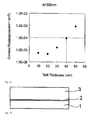
- Fig. 3 shows the relationship between the film thickness of TaN represented by the horizontal axis and the contact resistance represented by the vertical axis, where the film thickness of the Al layer 12 was set to 300 nm.
- the TaN/Al-based electrode had a contact resistance value of 1.0E-04 ⁇ cm -2 or less at a film thickness of TaN of 40 nm or less, and it was apparent that the electrode has ohmic characteristics.
- the film thickness of the Al layer 12 was restricted to 300 nm. However, for example, even when the film thickness of the Al layer is set to approximately 200 nm, it is assumed that the TaN/Al-based electrode will have ohmic characteristics as a result of setting the film thickness of TaN to 40 nm or less.
- the source electrode 9s and the drain electrode 9d serve as the TaN/Al electrodes, respectively, and are treated with heat at a temperature ranging from 520 to 600°C, and further, the film thickness of the TaN layer 11 is set to, for example, 40 nm or less, whereby ohmic contact with the active layer 3 can be attained.
- the buffer layer 2 composed of AlN or GaN and having a thickness of approximately 20 nm and the p-GaN layer 3 having a thickness of approximately 1 ⁇ m are sequentially grown on the substrate 1 made of, for example, sapphire, SiC, Si, GaN, or the like, by a metal organic chemical vapor deposition (MOCVD) method.
- MOCVD metal organic chemical vapor deposition
- Mg is used as p-type dopant, and the dopant concentration is set to, for example, 1 ⁇ 10 16 to 1 ⁇ 10 17 /cm 3 .
- the growth of GaN or the like on the substrate 1 is not limited to the MOCVD method and other growth methods such as a hydride vapor phase epitaxy (HVPE) method or a molecular beam epitaxy (MBE) method may be used.
- HVPE hydride vapor phase epitaxy
- MBE molecular beam epitaxy
- a photoresist 4 is applied to the p-GaN layer 3, and exposed to light and developed to form openings in each of a source region and a drain region.
- an n-type dopant such as silicon is injected to form the n+ type source region 5s and the n+ type drain region 5d.
- the concentration of the n-type dopant is set to, for example, 1 ⁇ 10 18 to 2 ⁇ 10 20 /cm 3 .
- a silicon oxide film (SiO 2 film) 6 is formed so as to have a thickness of approximately from 50 nm to 100 nm by a plasma-free catalytic chemical vapor deposition (Cat-CVD) method.
- Cat-CVD plasma-free catalytic chemical vapor deposition
- a conductive film 7 is formed on the silicon oxide film 6.
- Polysilicon is generally used for the conductive film 7, but the conductive film 7 is not restricted thereto, and may be a metal film such as Ni/Al or WSi.
- P phosphorous
- B boron
- polysilicon is grown by the CVD method, whereas, in the case of a metal film, it is formed by sputtering or the like.
- a photoresist 8 is applied to the conductive film 7 and is exposed to light and developed, as a result of which the photoresist 9 remains in the gate region but is removed from the source region 5s and the drain region 5d.
- etching is performed on the conductive film 7 and the silicon oxide film 6, and the conductive film 7 left on the gate region serves as the gate electrode 7g.
- the silicon oxide film 6 under the gate electrode 7g serves as the gate insulating film.
- the photoresist 8 is removed, and then, as shown in Fig. 1B , the TaN layer 11, which is to be the first layer in the source electrode 9s and the drain electrode 9d, is formed on the source region 5s and the drain region 5d by a facing target sputtering (facing sputtering) method.
- the Al layer 12 which is to be the second layer in the source electrode 9s and the drain electrode 9d, is formed on the TaN layer.
- the film thickness of the Al layer 12 was set to approximately 300 nm and the film thickness of the TaN layer 11 was set to 40 nm or less.
- heat treatment was performed in the range of from 520 to 600°C.
- each of the source electrode 9s and the drain electrode 9d can be in ohmic contact with the n+ GaN layer that forms the drain region 5d and the source region 5s.
- the first layer 11 in the source electrode 9s and the drain electrode 9d is made of tantalum nitride and thus is hardly oxidized. Accordingly, consecutive film formation of the first layer 11 and the second layer 12 is not necessary, and the first and the second layers 11 and 12 each can be film-formed by a single-target film formation apparatus. Since a multi-target film formation apparatus performs sputtering from an oblique direction, film quality tends to be poorer compared to the single-target film formation apparatus. Particularly, when a wafer having a large diameter is used, there has been a problem of reduced yield.
- the first layer 11 and the second layer 12 can be individually film-formed by the single-target film formation apparatus, whereby process flexibility is increased, and productivity can be improved.
- each of the source electrode 9s and the drain electrode 9d can be an ohmic electrode that are in ohmic contact with the source region 5s and the drain region 5d, respectively.
- the first layer 11 is made of tantalum nitride, electromigration can be suppressed even in a high temperature environment.
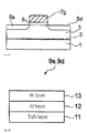
- Fig. 6A and Fig. 6B are each cross-sectional views showing another configuration of the source electrode 9s and the drain electrode 9d.
- a third layer 13 composed of W is formed on the second layer 12.
- the third layer 13 is not restricted to W and may be made of any one material selected from Ni, Pd, Mo, Ta, Ti, TaN, and TiN.
- formation of the third layer 13 reduces resistance of the metal itself, and can reduce resistance of the semiconductor transistor 10.
- a fourth layer 14 composed of Au is formed on the third layer 13.
- the source electrode 9s and the drain electrode 9d shown in Fig. 6B when Au is provided on the third layer 13, diffusion of Au is prevented. Additionally, since Au is provided on the surface, it is preferable, for example, to perform bonding or the like.
Landscapes
- Electrodes Of Semiconductors (AREA)
- Thin Film Transistor (AREA)
- Insulated Gate Type Field-Effect Transistor (AREA)
Abstract
Description
- The present invention relates to a method of producing a semiconductor transistor, and more particularly to a method of producing a semiconductor transistor involving formation of an ohmic electrode in ohmic contact with an active layer composed of a GaN-based semiconductor.
- As a gallium nitride-based semiconductor transistor (hereinafter referred to as a GaN-based semiconductor transistor), a GaN-based semiconductor transistor that has an ohmic electrode composed of Ti/Al on an active layer composed of a GaN-based semiconductor is known (for example, Japanese Patent Application Laid-Open (JP-A) No.
2002-359256 - With respect to this problem,
JP-A Nos. 2006-165207 2007-273545 4268099 - However, the Ti/Al electrode and the Ta/Al electrode are both problematic in that Ti and Ta have a tendency to be oxidized. Accordingly, when film formation of Ti (Ta) and Al is performed individually using a single target film formation device, there has been a problem of increased resistance due to the oxidation of the Ti (Ta).
- Therefore, it is necessary to consecutively perform film formation of Ti (Ta) and Al using a so-called multi-target film formation apparatus to form the Ti/Al electrode and the Ta/Al electrode. In the multi-target film-formation apparatus, however, sputtering of a target is performed from an oblique direction. Therefore, in the case of a wafer having a large diameter, uniformity of in-plane film thickness and the like of the wafer are adversely affected, thereby reducing yield.
- Patent Document 4 describes an ohmic electrode in which MoxGal-x is formed on TaN. However, formation of the ohmic electrode requires a heating treatment at 700°C or higher, and there are concerns about the effect of the heat on the GaN-based semiconductor.
- An object of the present invention is to provide a method of producing a semiconductor transistor in which an ohmic electrode that makes ohmic contact with an active layer can be formed, with an increased degree of freedom in terms of process.
- To achieve the object, the present invention provides a method of producing a semiconductor transistor involving formation of an ohmic electrode on an active layer composed of a GaN-based semiconductor, the method including:
- a process of forming a first layer composed of tantalum nitride on the active layer and a second layer composed of Al layered on the first layer; and
- a process of forming the ohmic electrode in ohmic contact with the active layer by heat treating the first layer and the second layer at a temperature of from 520°C to 600°C.
- The method of producing a semiconductor transistor of the present invention can form an ohmic electrode in ohmic contact with the active layer, with an increased degree of freedom in terms of process.
-
Fig. 1A is a cross-sectional view showing a configuration of the GaN-based semiconductor transistor according to an embodiment of the invention. -
Fig. 1B is a cross-sectional view showing a configuration of the GaN-based semiconductor transistor according to an embodiment of the invention. -
Fig. 2 is a chart showing the relationship between the ohmic characteristics of TaN/Al and the film thickness of TaN. -
Fig. 3 is a chart showing the relationship between the ohmic characteristics of TaN/Al and the temperature of the heat treatment. -
Fig. 4A is a view showing the process of producing the GaN-based semiconductor transistor according to an embodiment of the invention. -
Fig. 4B is a view showing the process of producing the GaN-based semiconductor transistor according to an embodiment of the invention. -
Fig. 4C is a view showing the process of producing the GaN-based semiconductor transistor according to an embodiment of the invention. -
Fig. 5A is a view showing the process of producing the GaN-based semiconductor transistor, following on fromFig. 4 . -
Fig. 5B is a view showing the process of producing the GaN-based semiconductor transistor, following on fromFig. 4 . -
Fig. 5C is a view showing the process of producing the GaN-based semiconductor transistor, following on fromFig. 4 . -
Fig. 6A is a cross-sectional view showing a configuration of another ohmic electrode. -
Fig. 6B is a cross-sectional view showing a configuration of another ohmic electrode. - Hereinafter, an exemplary embodiment of the present invention is described with reference to the drawings.
Fig. 1A and Fig. 1B are each cross-sectional views showing a configuration of a semiconductor transistor according to an embodiment of the invention. Asemiconductor transistor 10 is a GaN-based semiconductor transistor having an active layer composed of a GaN-based semiconductor. As shown inFig. 1A , thesemiconductor transistor 10 has abuffer layer 2 formed on asubstrate 1, a p-type active layer (p-GaN) 3 formed on thebuffer layer 2 using a group III nitride semiconductor, and a gateinsulating film 6 composed of a silicon oxide film formed on theactive layer 3. - In addition, the
semiconductor transistor 10 includes agate electrode 7g which is provided on theactive layer 3 with thegate insulating film 6 therebetween, and asource electrode 9s and adrain electrode 9d. Thesource electrode 9s and thedrain electrode 9d, which are provided suitably for thegate electrode 7g and are in ohmic contact with an n+type source region 5s and an n+type drain region 5d of theactive layer 3, respectively, are ohmic electrodes. - As shown in 1B, the
source electrode 9s and thedrain electrode 9d each have a TaN layer (first layer) 11 composed of tantalum nitride (TaN) formed on the n+type source region 5s and the n+type drain region 5d of theactive layer 3, respectively; and an Al layer (second layer) 12 composed of Al laminated on theTaN layer 11. - In consideration of the use of the GaN-based
semiconductor transistor 10 in a high temperature environment, the present inventors have conducted intensive and extensive investigation regarding ohmic electrode formation techniques with a view to suppressing electromigration and improving productivity. As a result, the present inventors have conceived of making the material of thefirst layer 11 TaN, in which Ta is nitrided to prevent oxidation of Ta, and of layering theAl layer 12 thereon, thereby forming the TaN/Al-based electrode. - In addition, the present inventors have found that the ohmic characteristics of the TaN/Al-based electrode depend on the temperature in a heat treatment (annealing) process.
-
Fig. 2 shows the relationship between the annealing temperature represented by the horizontal axis and the resistance Rch represented by the vertical axis, where the annealing time was 1 min. In the chart, for reference purposes, the resistance of the TaN/Al-based electrode in a case of performing annealing for 10 minutes at a temperature of 600°C is shown. As shown inFig. 2 , the TaN/Al-based electrode had a resistance value of 1.0E-04 Ω cm-2 or less at an annealing temperature of 520°C or more, and it was apparent that the electrode has ohmic characteristics. In contrast, an upper limit value of the annealing temperature was set to a temperature of 600°C or less, which does not exceed the melting point of Al. - Furthermore, the present inventors have found that the ohmic characteristics of the TaN/Al-based electrode also depend on the film thickness of TaN.
Fig. 3 shows the relationship between the film thickness of TaN represented by the horizontal axis and the contact resistance represented by the vertical axis, where the film thickness of theAl layer 12 was set to 300 nm. As shown inFig. 3 , the TaN/Al-based electrode had a contact resistance value of 1.0E-04 Ω cm-2 or less at a film thickness of TaN of 40 nm or less, and it was apparent that the electrode has ohmic characteristics. Herein, as one example, the film thickness of theAl layer 12 was restricted to 300 nm. However, for example, even when the film thickness of the Al layer is set to approximately 200 nm, it is assumed that the TaN/Al-based electrode will have ohmic characteristics as a result of setting the film thickness of TaN to 40 nm or less. - That is, the
source electrode 9s and thedrain electrode 9d serve as the TaN/Al electrodes, respectively, and are treated with heat at a temperature ranging from 520 to 600°C, and further, the film thickness of theTaN layer 11 is set to, for example, 40 nm or less, whereby ohmic contact with theactive layer 3 can be attained. - Hereinafter, a method of producing the
semiconductor transistor 10 is described. First, as shown inFig. 4A , thebuffer layer 2 composed of AlN or GaN and having a thickness of approximately 20 nm and the p-GaN layer 3 having a thickness of approximately 1 µm are sequentially grown on thesubstrate 1 made of, for example, sapphire, SiC, Si, GaN, or the like, by a metal organic chemical vapor deposition (MOCVD) method. For example, Mg is used as p-type dopant, and the dopant concentration is set to, for example, 1×10¹⁶ to 1×10¹⁷/cm3. The growth of GaN or the like on thesubstrate 1 is not limited to the MOCVD method and other growth methods such as a hydride vapor phase epitaxy (HVPE) method or a molecular beam epitaxy (MBE) method may be used. - Next, as shown in
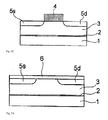
Fig. 4B , a photoresist 4 is applied to the p-GaN layer 3, and exposed to light and developed to form openings in each of a source region and a drain region. After that, through the openings, an n-type dopant such as silicon is injected to form the n+type source region 5s and the n+type drain region 5d. In this case, the concentration of the n-type dopant is set to, for example, 1×10¹⁸ to 2×10²⁰/cm3. - After the photoresist 4 is removed with a solvent, as shown in
Fig. 4C , for example, a silicon oxide film (SiO2 film) 6 is formed so as to have a thickness of approximately from 50 nm to 100 nm by a plasma-free catalytic chemical vapor deposition (Cat-CVD) method. - Next, as shown in
Fig. 5A , aconductive film 7 is formed on thesilicon oxide film 6. Polysilicon is generally used for theconductive film 7, but theconductive film 7 is not restricted thereto, and may be a metal film such as Ni/Al or WSi. In the case of using polysilicon, As, P (phosphorous), B (boron), or the like is doped and polysilicon is grown by the CVD method, whereas, in the case of a metal film, it is formed by sputtering or the like. - Furthermore, a
photoresist 8 is applied to theconductive film 7 and is exposed to light and developed, as a result of which the photoresist 9 remains in the gate region but is removed from thesource region 5s and thedrain region 5d. - Then, as shown in
Fig. 5B , using the patternedphotoresist 8 as a mask, etching is performed on theconductive film 7 and thesilicon oxide film 6, and theconductive film 7 left on the gate region serves as thegate electrode 7g. Thesilicon oxide film 6 under thegate electrode 7g serves as the gate insulating film. - Next, as shown in
Fig. 5C , thephotoresist 8 is removed, and then, as shown inFig. 1B , theTaN layer 11, which is to be the first layer in thesource electrode 9s and thedrain electrode 9d, is formed on thesource region 5s and thedrain region 5d by a facing target sputtering (facing sputtering) method. Next, by vacuum deposition, theAl layer 12, which is to be the second layer in thesource electrode 9s and thedrain electrode 9d, is formed on the TaN layer. Herein, the film thickness of theAl layer 12 was set to approximately 300 nm and the film thickness of theTaN layer 11 was set to 40 nm or less. Then, heat treatment was performed in the range of from 520 to 600°C. In this manner, each of thesource electrode 9s and thedrain electrode 9d can be in ohmic contact with the n+ GaN layer that forms thedrain region 5d and thesource region 5s. Through the above processes, thesemiconductor transistor 10 shown inFig. 1A can be produced. - In the method of producing the
semiconductor transistor 10 according to an embodiment of the invention, thefirst layer 11 in thesource electrode 9s and thedrain electrode 9d is made of tantalum nitride and thus is hardly oxidized. Accordingly, consecutive film formation of thefirst layer 11 and thesecond layer 12 is not necessary, and the first and thesecond layers - Thus, in the method of producing the
semiconductor transistor 10 according to an embodiment of the invention, thefirst layer 11 and thesecond layer 12 can be individually film-formed by the single-target film formation apparatus, whereby process flexibility is increased, and productivity can be improved. In addition, by performing the heat treatment in the range of from 520 to 600°C and by setting the film thickness of thefirst layer 11 to 40 nm or less, each of thesource electrode 9s and thedrain electrode 9d can be an ohmic electrode that are in ohmic contact with thesource region 5s and thedrain region 5d, respectively. Furthermore, since thefirst layer 11 is made of tantalum nitride, electromigration can be suppressed even in a high temperature environment. -
Fig. 6A and Fig. 6B are each cross-sectional views showing another configuration of thesource electrode 9s and thedrain electrode 9d. In Fig. 9A, athird layer 13 composed of W is formed on thesecond layer 12. Herein, thethird layer 13 is not restricted to W and may be made of any one material selected from Ni, Pd, Mo, Ta, Ti, TaN, and TiN. In thesource electrode 9s and thedrain electrode 9d shown inFig. 6A , formation of thethird layer 13 reduces resistance of the metal itself, and can reduce resistance of thesemiconductor transistor 10. - In
Fig. 6B , afourth layer 14 composed of Au is formed on thethird layer 13. In thesource electrode 9s and thedrain electrode 9d shown inFig. 6B , when Au is provided on thethird layer 13, diffusion of Au is prevented. Additionally, since Au is provided on the surface, it is preferable, for example, to perform bonding or the like. - Hereinabove, the present invention has been described based on a preferable embodiment. However, the method of producing a semiconductor transistor according to the present invention is not restricted simply to the configuration of this embodiment, and various changes and modifications in the configuration of the embodiment are also encompassed in the scope of the invention.
- The entire disclosure of Japanese Patent Application No.
2010-045548 - All publications, patent applications, and technical standards described in the present specification are incorporated herein by reference to the same extent as if each publication, patent application, or technical standard was specifically and individually indicated to be incorporated by reference.
Claims (4)
- A method of producing a semiconductor transistor involving formation of an ohmic electrode on an active layer composed of a GaN-based semiconductor, the method comprising:forming a first layer composed of tantalum nitride on the active layer and a second layer composed of Al layered on the first layer; andforming the ohmic electrode in ohmic contact with the active layer by heat treating the first and the second layers at a temperature of from 520°C to 600°C.
- The method of producing a semiconductor transistor according to claim 1, wherein a film thickness of the first layer is 40 nm or less.
- The method of producing a semiconductor transistor according to claim 1 or 2, further comprising forming a third layer composed of any one material selected from W, Ni, Pd, Mo, Ta, Ti, TaN, and TiN on the ohmic electrode.
- The method of producing a semiconductor transistor according to claim 3, further comprising forming a fourth layer composed ofAu on the third layer.
Applications Claiming Priority (2)
| Application Number | Priority Date | Filing Date | Title |
|---|---|---|---|
| JP2010045548A JP5437114B2 (en) | 2010-03-02 | 2010-03-02 | Manufacturing method of semiconductor transistor |
| PCT/JP2011/054814 WO2011108614A1 (en) | 2010-03-02 | 2011-03-02 | Semiconductor transistor production method |
Publications (2)
| Publication Number | Publication Date |
|---|---|
| EP2544224A1 true EP2544224A1 (en) | 2013-01-09 |
| EP2544224A4 EP2544224A4 (en) | 2014-06-25 |
Family
ID=44542261
Family Applications (1)
| Application Number | Title | Priority Date | Filing Date |
|---|---|---|---|
| EP11750723.6A Withdrawn EP2544224A4 (en) | 2010-03-02 | 2011-03-02 | METHOD FOR PRODUCING A SEMICONDUCTOR TRANSISTOR |
Country Status (5)
| Country | Link |
|---|---|
| US (1) | US8906796B2 (en) |
| EP (1) | EP2544224A4 (en) |
| JP (1) | JP5437114B2 (en) |
| CN (1) | CN102792422A (en) |
| WO (1) | WO2011108614A1 (en) |
Families Citing this family (3)
| Publication number | Priority date | Publication date | Assignee | Title |
|---|---|---|---|---|
| US9200365B2 (en) * | 2012-08-15 | 2015-12-01 | Applied Material, Inc. | Method of catalytic film deposition |
| US11222982B2 (en) * | 2016-09-29 | 2022-01-11 | Intel Corporation | Methods and apparatus to form silicon-based transistors on group III-nitride materials using aspect ratio trapping |
| CN108231565A (en) * | 2017-12-07 | 2018-06-29 | 华南理工大学 | The preparation method of the Ohmic contact of GaN high electron mobility transistor |
Family Cites Families (13)
| Publication number | Priority date | Publication date | Assignee | Title |
|---|---|---|---|---|
| JPH053168A (en) * | 1991-06-25 | 1993-01-08 | Toshiba Corp | Method of forming semiconductor electrode |
| DE69617192T2 (en) * | 1995-08-24 | 2002-07-18 | Sony Corp., Tokio/Tokyo | LAMINATE AND METHOD FOR PRODUCING AN OHMS ELECTRODE |
| JPH11330546A (en) * | 1998-05-12 | 1999-11-30 | Fuji Electric Co Ltd | Group III nitride semiconductor and method of manufacturing the same |
| JP3846150B2 (en) * | 2000-03-27 | 2006-11-15 | 豊田合成株式会社 | Group III nitride compound semiconductor device and electrode forming method |
| JP4663156B2 (en) | 2001-05-31 | 2011-03-30 | 富士通株式会社 | Compound semiconductor device |
| JP4268099B2 (en) | 2004-07-16 | 2009-05-27 | 富士通株式会社 | Nitride-based compound semiconductor device and manufacturing method thereof |
| JP5216184B2 (en) | 2004-12-07 | 2013-06-19 | 富士通株式会社 | Compound semiconductor device and manufacturing method thereof |
| JP4841844B2 (en) * | 2005-01-05 | 2011-12-21 | 三菱電機株式会社 | Semiconductor element |
| KR100719379B1 (en) | 2006-03-30 | 2007-05-17 | 삼성전자주식회사 | Nonvolatile memory device |
| JP5231719B2 (en) * | 2006-03-30 | 2013-07-10 | 富士通株式会社 | Method for manufacturing field effect transistor |
| JP5462161B2 (en) * | 2007-07-20 | 2014-04-02 | アイメック | Method for manufacturing damascene contact in III-V group MESFET |
| JP5324076B2 (en) * | 2007-11-21 | 2013-10-23 | シャープ株式会社 | Schottky electrode for nitride semiconductor and nitride semiconductor device |
| JP2010045548A (en) | 2008-08-11 | 2010-02-25 | Ntt Docomo Inc | Base station, mobile station, signal transmitting method and signal receiving method |
-
2010
- 2010-03-02 JP JP2010045548A patent/JP5437114B2/en active Active
-
2011
- 2011-03-02 US US13/582,239 patent/US8906796B2/en active Active
- 2011-03-02 WO PCT/JP2011/054814 patent/WO2011108614A1/en not_active Ceased
- 2011-03-02 CN CN2011800118756A patent/CN102792422A/en active Pending
- 2011-03-02 EP EP11750723.6A patent/EP2544224A4/en not_active Withdrawn
Also Published As
| Publication number | Publication date |
|---|---|
| US20130052816A1 (en) | 2013-02-28 |
| EP2544224A4 (en) | 2014-06-25 |
| JP5437114B2 (en) | 2014-03-12 |
| US8906796B2 (en) | 2014-12-09 |
| WO2011108614A1 (en) | 2011-09-09 |
| JP2011181753A (en) | 2011-09-15 |
| CN102792422A (en) | 2012-11-21 |
Similar Documents
| Publication | Publication Date | Title |
|---|---|---|
| US10896969B2 (en) | Manufacturing method of an HEMT transistor of the normally off type with reduced resistance in the on state and HEMT transistor | |
| US9875899B2 (en) | Semiconductor transistor | |
| TW201212286A (en) | Method for manufacturing nitride semiconductor crystal layer | |
| US9934978B2 (en) | Method of fabricating an electrical contact for use on a semiconductor device | |
| JP2008135700A (en) | Group III nitride film manufacturing method and group III nitride semiconductor device | |
| JP5303948B2 (en) | Ohmic electrode forming method and method of manufacturing field effect transistor | |
| CN111527587B (en) | Preparation method of Group III nitride semiconductor substrate | |
| JP4889203B2 (en) | Nitride semiconductor device and manufacturing method thereof | |
| JP5242156B2 (en) | III-V nitride compound semiconductor device and electrode forming method | |
| US8906796B2 (en) | Method of producing semiconductor transistor | |
| WO2015045628A1 (en) | Method for manufacturing silicon-carbide semiconductor device | |
| JP2011210780A (en) | GaN-MIS TRANSISTOR, GaN-IGBT AND METHOD FOR MANUFACTURING THEM | |
| TWI890939B (en) | Nucleation layers for growth of gallium-and-nitrogen-containing regions | |
| JP2006165207A (en) | Compound semiconductor device and manufacturing method thereof | |
| JP5090968B2 (en) | Method for manufacturing silicon carbide semiconductor device | |
| WO2015115126A1 (en) | Nitride semiconductor laminate, method for producing same and nitride semiconductor device | |
| JP6519920B2 (en) | Method of manufacturing semiconductor substrate, and method of manufacturing semiconductor device | |
| JP2005268507A (en) | Field effect transistor and manufacturing method thereof | |
| JP2008112750A (en) | Semiconductor device manufacturing method | |
| JP2009224643A (en) | Field-effect transistor and its manufacturing method | |
| JP5431756B2 (en) | Semiconductor device made of group III nitride semiconductor | |
| JP2010016105A (en) | HEAT TREATMENT METHOD FOR GaN-BASED DEVICE ON Si SUBSTRATE | |
| JP2007123824A (en) | Electronic device using group III nitride compound semiconductor | |
| JP6582736B2 (en) | Manufacturing method of nitride semiconductor device | |
| JP2011258781A (en) | Manufacturing method of field-effect semiconductor device |
Legal Events
| Date | Code | Title | Description |
|---|---|---|---|
| PUAI | Public reference made under article 153(3) epc to a published international application that has entered the european phase |
Free format text: ORIGINAL CODE: 0009012 |
|
| 17P | Request for examination filed |
Effective date: 20120913 |
|
| AK | Designated contracting states |
Kind code of ref document: A1 Designated state(s): AL AT BE BG CH CY CZ DE DK EE ES FI FR GB GR HR HU IE IS IT LI LT LU LV MC MK MT NL NO PL PT RO RS SE SI SK SM TR |
|
| DAX | Request for extension of the european patent (deleted) | ||
| RAP1 | Party data changed (applicant data changed or rights of an application transferred) |
Owner name: TOHOKU UNIVERSITY Owner name: FUJI ELECTRIC CO., LTD. Owner name: FURUKAWA ELECTRIC CO., LTD. |
|
| A4 | Supplementary search report drawn up and despatched |
Effective date: 20140526 |
|
| RIC1 | Information provided on ipc code assigned before grant |
Ipc: H01L 29/45 20060101ALI20140520BHEP Ipc: H01L 29/20 20060101ALN20140520BHEP Ipc: H01L 29/78 20060101ALN20140520BHEP Ipc: H01L 21/285 20060101AFI20140520BHEP Ipc: H01L 21/336 20060101ALN20140520BHEP Ipc: H01L 21/28 20060101ALN20140520BHEP |
|
| RAP1 | Party data changed (applicant data changed or rights of an application transferred) |
Owner name: TOHOKU UNIVERSITY Owner name: FURUKAWA ELECTRIC CO., LTD. |
|
| STAA | Information on the status of an ep patent application or granted ep patent |
Free format text: STATUS: THE APPLICATION IS DEEMED TO BE WITHDRAWN |
|
| 18D | Application deemed to be withdrawn |
Effective date: 20141224 |