EP2544029B1 - Künstliches dielektrisches material - Google Patents
Künstliches dielektrisches material Download PDFInfo
- Publication number
- EP2544029B1 EP2544029B1 EP11860700.1A EP11860700A EP2544029B1 EP 2544029 B1 EP2544029 B1 EP 2544029B1 EP 11860700 A EP11860700 A EP 11860700A EP 2544029 B1 EP2544029 B1 EP 2544029B1
- Authority
- EP
- European Patent Office
- Prior art keywords
- artificial
- substrate
- metamaterial
- carbon nanotube
- transparent
- Prior art date
- Legal status (The legal status is an assumption and is not a legal conclusion. Google has not performed a legal analysis and makes no representation as to the accuracy of the status listed.)
- Active
Links
Images


Classifications
-
- G—PHYSICS
- G02—OPTICS
- G02B—OPTICAL ELEMENTS, SYSTEMS OR APPARATUS
- G02B1/00—Optical elements characterised by the material of which they are made; Optical coatings for optical elements
- G02B1/002—Optical elements characterised by the material of which they are made; Optical coatings for optical elements made of materials engineered to provide properties not available in nature, e.g. metamaterials
-
- B—PERFORMING OPERATIONS; TRANSPORTING
- B82—NANOTECHNOLOGY
- B82Y—SPECIFIC USES OR APPLICATIONS OF NANOSTRUCTURES; MEASUREMENT OR ANALYSIS OF NANOSTRUCTURES; MANUFACTURE OR TREATMENT OF NANOSTRUCTURES
- B82Y20/00—Nanooptics, e.g. quantum optics or photonic crystals
-
- B—PERFORMING OPERATIONS; TRANSPORTING
- B82—NANOTECHNOLOGY
- B82Y—SPECIFIC USES OR APPLICATIONS OF NANOSTRUCTURES; MEASUREMENT OR ANALYSIS OF NANOSTRUCTURES; MANUFACTURE OR TREATMENT OF NANOSTRUCTURES
- B82Y30/00—Nanotechnology for materials or surface science, e.g. nanocomposites
-
- B—PERFORMING OPERATIONS; TRANSPORTING
- B82—NANOTECHNOLOGY
- B82Y—SPECIFIC USES OR APPLICATIONS OF NANOSTRUCTURES; MEASUREMENT OR ANALYSIS OF NANOSTRUCTURES; MANUFACTURE OR TREATMENT OF NANOSTRUCTURES
- B82Y40/00—Manufacture or treatment of nanostructures
-
- C—CHEMISTRY; METALLURGY
- C01—INORGANIC CHEMISTRY
- C01B—NON-METALLIC ELEMENTS; COMPOUNDS THEREOF; METALLOIDS OR COMPOUNDS THEREOF NOT COVERED BY SUBCLASS C01C
- C01B32/00—Carbon; Compounds thereof
- C01B32/15—Nano-sized carbon materials
- C01B32/158—Carbon nanotubes
-
- H—ELECTRICITY
- H01—ELECTRIC ELEMENTS
- H01Q—ANTENNAS, i.e. RADIO AERIALS
- H01Q15/00—Devices for reflection, refraction, diffraction or polarisation of waves radiated from an antenna, e.g. quasi-optical devices
- H01Q15/0006—Devices acting selectively as reflecting surface, as diffracting or as refracting device, e.g. frequency filtering or angular spatial filtering devices
- H01Q15/0013—Devices acting selectively as reflecting surface, as diffracting or as refracting device, e.g. frequency filtering or angular spatial filtering devices said selective devices working as frequency-selective reflecting surfaces, e.g. FSS, dichroic plates, surfaces being partly transmissive and reflective
- H01Q15/0026—Devices acting selectively as reflecting surface, as diffracting or as refracting device, e.g. frequency filtering or angular spatial filtering devices said selective devices working as frequency-selective reflecting surfaces, e.g. FSS, dichroic plates, surfaces being partly transmissive and reflective said selective devices having a stacked geometry or having multiple layers
-
- H—ELECTRICITY
- H01—ELECTRIC ELEMENTS
- H01Q—ANTENNAS, i.e. RADIO AERIALS
- H01Q15/00—Devices for reflection, refraction, diffraction or polarisation of waves radiated from an antenna, e.g. quasi-optical devices
- H01Q15/0006—Devices acting selectively as reflecting surface, as diffracting or as refracting device, e.g. frequency filtering or angular spatial filtering devices
- H01Q15/006—Selective devices having photonic band gap materials or materials of which the material properties are frequency dependent, e.g. perforated substrates, high-impedance surfaces
-
- H—ELECTRICITY
- H01—ELECTRIC ELEMENTS
- H01Q—ANTENNAS, i.e. RADIO AERIALS
- H01Q15/00—Devices for reflection, refraction, diffraction or polarisation of waves radiated from an antenna, e.g. quasi-optical devices
- H01Q15/02—Refracting or diffracting devices, e.g. lens, prism
- H01Q15/08—Refracting or diffracting devices, e.g. lens, prism formed of solid dielectric material
-
- G—PHYSICS
- G02—OPTICS
- G02B—OPTICAL ELEMENTS, SYSTEMS OR APPARATUS
- G02B5/00—Optical elements other than lenses
- G02B5/008—Surface plasmon devices
-
- G—PHYSICS
- G02—OPTICS
- G02F—OPTICAL DEVICES OR ARRANGEMENTS FOR THE CONTROL OF LIGHT BY MODIFICATION OF THE OPTICAL PROPERTIES OF THE MEDIA OF THE ELEMENTS INVOLVED THEREIN; NON-LINEAR OPTICS; FREQUENCY-CHANGING OF LIGHT; OPTICAL LOGIC ELEMENTS; OPTICAL ANALOGUE/DIGITAL CONVERTERS
- G02F2202/00—Materials and properties
- G02F2202/30—Metamaterials
-
- G—PHYSICS
- G02—OPTICS
- G02F—OPTICAL DEVICES OR ARRANGEMENTS FOR THE CONTROL OF LIGHT BY MODIFICATION OF THE OPTICAL PROPERTIES OF THE MEDIA OF THE ELEMENTS INVOLVED THEREIN; NON-LINEAR OPTICS; FREQUENCY-CHANGING OF LIGHT; OPTICAL LOGIC ELEMENTS; OPTICAL ANALOGUE/DIGITAL CONVERTERS
- G02F2202/00—Materials and properties
- G02F2202/36—Micro- or nanomaterials
-
- G—PHYSICS
- G02—OPTICS
- G02F—OPTICAL DEVICES OR ARRANGEMENTS FOR THE CONTROL OF LIGHT BY MODIFICATION OF THE OPTICAL PROPERTIES OF THE MEDIA OF THE ELEMENTS INVOLVED THEREIN; NON-LINEAR OPTICS; FREQUENCY-CHANGING OF LIGHT; OPTICAL LOGIC ELEMENTS; OPTICAL ANALOGUE/DIGITAL CONVERTERS
- G02F2202/00—Materials and properties
- G02F2202/40—Materials having a particular birefringence, retardation
-
- Y—GENERAL TAGGING OF NEW TECHNOLOGICAL DEVELOPMENTS; GENERAL TAGGING OF CROSS-SECTIONAL TECHNOLOGIES SPANNING OVER SEVERAL SECTIONS OF THE IPC; TECHNICAL SUBJECTS COVERED BY FORMER USPC CROSS-REFERENCE ART COLLECTIONS [XRACs] AND DIGESTS
- Y10—TECHNICAL SUBJECTS COVERED BY FORMER USPC
- Y10T—TECHNICAL SUBJECTS COVERED BY FORMER US CLASSIFICATION
- Y10T428/00—Stock material or miscellaneous articles
- Y10T428/24—Structurally defined web or sheet [e.g., overall dimension, etc.]
- Y10T428/24802—Discontinuous or differential coating, impregnation or bond [e.g., artwork, printing, retouched photograph, etc.]
-
- Y—GENERAL TAGGING OF NEW TECHNOLOGICAL DEVELOPMENTS; GENERAL TAGGING OF CROSS-SECTIONAL TECHNOLOGIES SPANNING OVER SEVERAL SECTIONS OF THE IPC; TECHNICAL SUBJECTS COVERED BY FORMER USPC CROSS-REFERENCE ART COLLECTIONS [XRACs] AND DIGESTS
- Y10—TECHNICAL SUBJECTS COVERED BY FORMER USPC
- Y10T—TECHNICAL SUBJECTS COVERED BY FORMER US CLASSIFICATION
- Y10T428/00—Stock material or miscellaneous articles
- Y10T428/24—Structurally defined web or sheet [e.g., overall dimension, etc.]
- Y10T428/24942—Structurally defined web or sheet [e.g., overall dimension, etc.] including components having same physical characteristic in differing degree
Definitions
- the present invention relates to material, and particularly to an artificial metamaterial.
- Metamaterials are new synthetic artificial materials which can generate responses to electromagnetic waves, composed of at least one substrate and a plurality of artificial microstructures embedded into the substrate.
- the artificial microstructures are usually made from metal wires and configured into a certain geometric structure. Therefore, the artificial microstructure is capable of generating responses to electromagnetic waves. Therefore the metamaterials usually perform electromagnetic properties which are different from electromagnetic properties of the substrate.
- the electromagnetic properties can achieve some special functions that common materials can not achieve, such as to achieve convergence or divergence for electromagnetic waves and so on. It can be applied in the electromagnetic communication filed such as the antennas and radars.
- the metamaterial can be applied to electromagnetic waves of different frequency ranges, however currently application fields for the metamaterial are usually limited to the electromagnetic communication field while inoperative to visible light wave. This is limited by the materials of the substrate and the material of the artificial microstructures. If the problem that using the metamaterials for convergence, divergence for the visible light wave is solved, the application range of the metamaterials can be extended to visible light wave.
- an artificial metamaterial as set out in claim 1.
- the artificial metamaterial includes at least one material sheet, each material sheet including a laminary substrate and a plurality of artificial microstructures attached to the substrate.
- the substrate is made from transparent material.
- the substrate can be made from transparent polymer material.
- the substrate can be made from polymethyl methacrylate.
- the substrate can be made from transparent polyurethane, polyethylene, polyethylene glycol terephthalate or PVC.
- the light transmittance of the artificial electromagnetic material can be equal to or greater than 85 % .
- the artificial microstructure is a carbon nanotube film with a geometric pattern.
- a light transmittance of the carbon nanotube film can be equal to or greater than 80%.
- the thickness of the carbon nanotube film can range from 50 to 1000nm.
- the carbon nanotube film includes an ion conductive polymer adhesive and carbon nanotubes are dispersed in the electrical conductive polymer adhesive.
- Refractive indexes of the material sheet can vary according to a number of concentric circles.
- Each substrate can be virtually divided into a variety of substrate units arranged in an array.
- One artificial microstructure can be attached to each of substrate units respectively.
- a material unit may be composed of a substrate unit and an artificial microstructure attached to the substrate unit.
- the material unit in the center of material sheet can be treated as the center of the concentric circles.
- Material units which have the same distance to the center of the concentric circles can be positioned on the same circle.
- the refractive indexes of material units positioned on the same circle may be the same.
- the refractive indexes of the material units may decrease when the radius of the circle increases. Refractive index difference value between two adjacent circles may gradually increases when the radiuses of the circles increase.
- Each of material sheets can include a plurality of artificial microstructures.
- the plurality of artificial microstructures may be attached to the substrate arranged in an array.
- the sizes of the plurality of artificial microstructures may decrease along one direction of the array.
- the artificial metamaterial of the invention has the following beneficial effects: because the substrate is made from transparent materials, therefore is capable of generating responses to visible light wave, which causing convergence, divergence, deflection and so on.
- the artificial metamaterial 100 includes at least one material sheet 1. If there are several material sheets 1, the material sheets are stacked along the X direction perpendicular to the outer surface to form into one whole.
- Each material sheet 1 includes a laminary substrate 3 and a plurality of artificial microstructures 4 attached to the laminary substrate 3.
- the laminary substrate 3 is virtually divided into a plurality of identical rectangular grids. Each grid is a substrate unit 30, and an artificial microstructure 4 is attached to each substrate unit 30.
- a material unit 2 is composed of a substrate unit 30 and an artificial microstructure 4 attached to the substrate unit 30.
- the material sheet 1 can be defined as a plurality of material units 2 arranged in an array.
- the Z direction is defined as a direction of rows and the Y direction is defined as a direction of columns.
- the size of rectangular grid can be freely determined.
- the lengths of the grid along the directions Y, Z are both one tenth of the wavelength of electromagnetic wave to be converged.
- the length of the grid along the direction X is equal to the thickness of the substrate sheet 3 in the direction X.
- the lengths of the material unit along the direction X, Y, Z direction can be one fifty to one half of the wavelength of electromagnetic wave to be converged.
- Each material unit 2 includes a substrate unit 30 and an artificial microstructure 4 attached to the surface of the substrate unit 30.
- the artificial microstructure 4 is in a planar "I" shaped and made from metal wires.
- the artificial microstructure 4 includes a first metal wire in straight line and two second metal wires which are respectively perpendicularly connected with the two ends of the first metal wire.
- the artificial microstructure 4 can also be other shapes, such as a flat two-dimensional snowflake shape, which includes two first metal wires and four second metal wires.
- the first metal wires are mutually orthogonal.
- Each first metal wire includes two ends.
- Each second metal wire is perpendicularly connected to one end of each first metal wire.
- the artificial microstructure 4 further can be a three-dimensional snowflake shape, which includes three first metal wires and six second metal wires. Every two first metal wires are mutually orthogonal such the three first metal wires intersect at a same point. Each first metal wire includes two ends. Each second metal wire is perpendicularly connected to one ends of each first metal wire.
- the three-dimensional artificial microstructure 4 can be attached to the inside of the substrate 3 through a certain processing technology.
- Each substrate unit 30 and the artificial microstructure 4 attached to the each substrate unit 30 cooperatively determined the permittivity and permeability of the material unit 2 which is composed of them.
- n ⁇
- the refractive index n can be obtained.
- the size of refractive index indicates the influence degree in the direction of electromagnetic wave propagation. Therefore through design of shape and size of each artificial microstructure and so on, it can change the permittivity and permeability of each material unit 2, such to obtain certain refractive index distribution to achieve the deflection, convergence or divergence of the electromagnetic wave and so on.
- the artificial microstructure 4 can usually made from silver, copper and other materials of non-ferrous metal. Because silver and copper are good conductors. A surface plasma effect is generated on the surface of metal structure. The good conductors also can stimulate and enhance the surface plasma effect as much as possible and thus the electromagnetic wave response is more sensitive and the effect is stronger.
- the substrate 3 is required to be chosen from the materials which cannot generate response and influence for electromagnetic wave or the influence is as lower as possible.
- the permittivity and permeability must be close to 1 as much as possible.
- Ceramic is usually chosen as a material for the substrate of the conventional artificial metamaterials.
- the artificial electromagnetic material shows the electromagnetic characteristic which common nature materials without, such as negative refraction, convergent beam, deflection beam, and beam parallel characteristics. According to physical characteristics, it extends many new applications, such as in communication, optics, device miniaturization, and detection and so on.
- the conventional artificial metamaterials are mainly applied in microwave band and can not have the effect to visible light wave.
- transparent means that the light transmittance of a material is equal to or greater than 85%.
- the first innovation point of the invention is that the transparent materials are used for substrate 3, such as transparent organic polymer materials and so on.
- the transparent organic glass namely polymethyl methacrylate of which an abbreviated form is PMMA, is used for the substrate 3 of the invention.
- the other transparent organic polymer materials used for the substrate 3 also can be transparent polyurethane, polyethylene (PE), low density polyethylene (LDPE), polypropylene (PP), polyethylene glycol terephthalate (PET), polyvinyl chloride (PVC) and so on.
- the dielectric constant of these materials used for the substrate is not high and is chosen from 1 to 3.
- the permeability is substantially 1. It meets the premise requirement of substrate 3.
- these materials can be transparent or translucent through current technologies of the manufacturing process to let visible light wave travels through.
- the second innovation point of the invention is that the artificial micro structure 4 is also made from transparent or translucent materials.
- the artificial metamaterial When manufacturing the artificial metamaterial, transparent polymer materials such as the transparent organic glass can be used for substrate 3.
- a variety of artificial microstructures 4 are formed on the surface of the substrate 3 by electron beam evaporation, physical vapor deposition, or sputtering deposition technologies such as to form a material sheet 1.
- Several material sheets 1 can be encapsulated to be a whole piece of the artificial metamaterial. Because the substrate 3 and the artificial microstructures 4 are transparent material, therefore the artificial metamaterial can be used in visible light wave field. It can greatly expand the application fields and the application ranges of the artificial metamaterials. It has important scientific value and economic value.
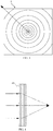
- the refractive index of material sheet varies according to a number of concentric circles, as shown in FIG. 3 .
- the material unit 2 in the center of material sheet is treated as the center of the concentric circles.
- Material units 2 which have the same distance to the center of the concentric circles are positioned on the same circle.
- the refractive indexes of materials units positioned on the same circle are the same.
- the refractive indexes of the material units positioned in the same circle decrease when the radius of the circle increases. Refractive index difference between two adjacent neighbored circles gradually increases when the radiuses of the circles increase.
- the material sheet 1 with the refractive index varies according to a number of concentric circles meets the condition can achieve the convergence of the electromagnetic wave.
- the artificial microstructure 4 with the same shape the smaller the artificial microstructure is, the lower the refractive index of corresponding material unit 2 is.
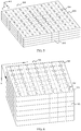
- FIG. 4 As shown in FIG. 4 , several material sheets 1 of FIG. 3 are stacked to form an artificial metamaterial 100.
- a parallel beam of visible light wave can travel through the transparent substrate 3 and the artificial microstructures 4.
- the refractive indexes vary according to a number of concentric circles which the material units 2 positioned make the visible light wave converge to a point to achieve the similar function of a convex lens.
- the difference between the artificial metamaterial 200 provided in an embodiment of the invention and the artificial metamaterial of FIGs. 1 and 2 is that the artificial metamaterial 200 of the artificial microstructure 204 is carbon nanotube film.
- carbon nanotube As a new material, carbon nanotube is very light and has high strength characteristics. More importantly, carbon nanotube has excellent conductive property. When the diameter of the carbon nanotube is less than 6 nanometers (nm), it can be treated as one-dimensional quantum conductive wire with good electrically conductivity.
- the carbon nanotube film of the invention is one type of film which contains carbon nanotubes.
- the carbon nanotube includes an ion conductive polymer adhesive and carbon nanotubes dispersed in the adhesive.
- the adhesive is sulfonyl fluorinated polyethylene, or as carboxyl group, the acyl phosphate or sub sulfamoyl of thermoplastic polymer.
- the thickness of the carbon nanotube film is ranged from 50 to 1000nm.
- the carbon nanotube is transparent and colorless and has good electrical conductivity, therefore can be used as the conductive film to replace silver and copper to make the artificial microstructure respond to the electromagnetic wave. At the same time, it also has good light transmittance, such applications of artificial metamaterial can be extended from microwave field to visible light wave field.
- carbon nanotube is dispersed in aqueous solvent to form carbon nanotube solution and the ion conducting polymer adhesive is dissolved in ethanol solvent to form ion conducting polymer adhesive water solution. Then the carbon nanotube solution is mixed with the ionic conductive polymer adhesive solution. The mixed solution is stirred by an agitator. Then the stirred solution is coated onto the substrate 203 made from transparent organic glass of polymer material. Water and ethanol vaporize and carbon nanotube film is formed being adhered to the substrate. The carbon nanotube film forms the artificial microstructure 204. Each of the artificial microstructures 204 can be coated according to a certain designation, therefore making a material sheet 201. At last multiply of material sheets 201 are encapsulated into a whole of artificial metamaterial.
- the mainly difference between the artificial metamaterial 300 and the artificial metamaterial of FIGs. 1 and 2 is, aluminum doped zinc oxide thin film is used in the artificial microstructure 304 of the artificial metamaterial 300.
- ZAO film Aluminum doped zinc oxide (abbreviation for ZAO) film, is get from Al doped in ZnO system.
- ZnO film has many grains with C axis preferentially growth. Each of grains is hexagonal lead-zinc mine structure with good growth.
- ZnO crystal is composed of oxygen six angle close-packed and zinc six angle compactly-stacked and reversely nested. The structure of the film has transparent conductivity, however the resistance is great.
- Al doped in ZnO ZAO film can be formed and the electrical resistivity is greatly reduced. Therefore it has good conductive performance, at the same time the stability of the film is greatly improved.
- the thickness of the aluminum doped zinc oxide is usually ranged from 50 to 1000nm.
- the aluminum doped zinc oxide is transparent and colorless.
- the light transmittance is reached to 90%. Because of good electrical conductivity, it can be used as conductive film to replace silver and copper to make artificial microstructure respond to the electromagnetic wave. At the same time, application can extended from microwave field to the visible light wave for good light transmittance of the metamaterial.
- the substrate 303 made from transparent polymer materials such as the transparent organic glass is firstly prepared, a protection film is attached to the substrate 303.
- the protection film defines a plurality of through holes with the same shape as the artificial microstructure.
- ZAO can be deposited on the protection film through evaporation. The ZAO will be directly attached to the substrate 3 by the through holes.
- the substrate attached with the artificial microstructure made from ZAO film is obtained. Therefore a material sheet 301 is obtained. At last several material sheets 301 are encapsulated into a complete artificial metamaterial 300.
- the artificial microstructures of each of columns are the same, and along the Z direction the artificial microstructures of each of columns have the same geometric shape while the size gradually decreases.
- the refractive index along X and Y direction keeps the same and the refractive index along Z direction gradually decreases.
- the material sheet 1 which meets the refractive index distribution can achieve the electromagnetic deflection. As shown in FIG. 7 , the electromagnetic wave traveling from low refractive index to the transparent synthetic material will be deflected to the high refractive index direction.
- the electromagnetic wave can be extended from microwave band to visible light band. It is a revolutionary progress and useful to replace the traditional optical elements such as convex lens, concave mirror, and the material sheet of the invention is planar board without the need for special designations of convex or concave or complex surface. It greatly simplify the designation process and manufacturing process. It can effectively reduce the costs of designation and manufacturing.
Landscapes
- Chemical & Material Sciences (AREA)
- Engineering & Computer Science (AREA)
- Nanotechnology (AREA)
- Physics & Mathematics (AREA)
- Optics & Photonics (AREA)
- General Physics & Mathematics (AREA)
- Crystallography & Structural Chemistry (AREA)
- Materials Engineering (AREA)
- Condensed Matter Physics & Semiconductors (AREA)
- Organic Chemistry (AREA)
- Composite Materials (AREA)
- Manufacturing & Machinery (AREA)
- Life Sciences & Earth Sciences (AREA)
- Biophysics (AREA)
- Inorganic Chemistry (AREA)
- Laminated Bodies (AREA)
- Shielding Devices Or Components To Electric Or Magnetic Fields (AREA)
Claims (4)
- Künstliches Metamaterial, das Folgendes umfasst:zumindest eine Materiallage (1), wobei jede Materiallage (1) ein Laminatsubstrat (3) und eine Vielzahl von künstlichen Mikrostrukturen (4), die auf dem Substrat (3) befestigt sind, umfasst, wobeidas Substrat (3) aus transparentem Material hergestellt ist, wobeijede künstliche Mikrostruktur (4) ein Kohlenstoffnanoröhrenfilm mit einer geometrischen Struktur ist, wobeijeder Kohlenstoffnanoröhrenfilm ein elektrisch leitendes Polymerhaftmittel umfasst, das darin dispergierte Kohlenstoffnanoröhren aufweist, wobeidas elektrisch leitende Polymerhaftmittel sulfonylfluoriertes Polyethylen oder, als Carboxylgruppe, Acylphosphat oder Subsulfamoyl von thermoplastischem Polymer ist, undwobei jede künstliche Mikrostruktur (4) eine planare "I"-Form aufweist, die einen ersten Draht in einer geraden Linie und zwei zweite Drähte, die an entsprechenden Enden des ersten Drahts im rechten Winkel verbunden sind umfasst.
- Künstliches Metamaterial nach Anspruch 1, wobei das Substrat aus transparentem Polymermaterial hergestellt ist.
- Künstliches Metamaterial nach Anspruch 2, wobei das Substrat aus Polymethylmethacrylat, transparentem Polyurethan, Polyethylen, Polyethylenglykolterephthalat oder PVC hergestellt ist.
- Künstliches Metamaterial nach Anspruch 1, wobei eine Dicke des Kohlenstoffnanoröhrenfilms 500 bis 1000 nm beträgt und die Lichtdurchlässigkeit des Kohlenstoffnanoröhrenfilms gleich oder größer 80 % ist.
Applications Claiming Priority (4)
| Application Number | Priority Date | Filing Date | Title |
|---|---|---|---|
| CN 201110091287 CN102480006B (zh) | 2011-04-12 | 2011-04-12 | 一种透明超材料 |
| CN201110120011.XA CN102778705B (zh) | 2011-05-10 | 2011-05-10 | 一种透明超材料 |
| CN201110120041.0A CN102890992B (zh) | 2011-05-10 | 2011-05-10 | 一种透明人工电磁材料 |
| PCT/CN2011/081389 WO2012139368A1 (zh) | 2011-04-12 | 2011-10-27 | 一种人工电磁材料 |
Publications (3)
| Publication Number | Publication Date |
|---|---|
| EP2544029A1 EP2544029A1 (de) | 2013-01-09 |
| EP2544029A4 EP2544029A4 (de) | 2015-04-01 |
| EP2544029B1 true EP2544029B1 (de) | 2019-12-25 |
Family
ID=47008814
Family Applications (1)
| Application Number | Title | Priority Date | Filing Date |
|---|---|---|---|
| EP11860700.1A Active EP2544029B1 (de) | 2011-04-12 | 2011-10-27 | Künstliches dielektrisches material |
Country Status (3)
| Country | Link |
|---|---|
| US (1) | US9268062B2 (de) |
| EP (1) | EP2544029B1 (de) |
| WO (1) | WO2012139368A1 (de) |
Families Citing this family (7)
| Publication number | Priority date | Publication date | Assignee | Title |
|---|---|---|---|---|
| JP2014145982A (ja) * | 2013-01-30 | 2014-08-14 | Toshiba Corp | 光学装置、固体撮像装置及び光学装置の製造方法 |
| CN106405972B (zh) * | 2016-10-28 | 2019-02-01 | 同济大学 | 一种磁控可调频远红外光开关及其实现方法 |
| CN115117633B (zh) * | 2021-03-19 | 2025-10-31 | 深圳光启尖端技术有限责任公司 | 超材料和飞行器 |
| CN113328261B (zh) * | 2021-05-11 | 2022-11-08 | 中国科学院上海光学精密机械研究所 | 基于齿状弯折环和方形环的双谐振宽带透明超材料吸波器 |
| CN116470300A (zh) * | 2023-05-15 | 2023-07-21 | 上海大学 | 一种具有光学透明特性的宽带微波吸收材料及其应用 |
| WO2025125169A1 (en) * | 2023-12-11 | 2025-06-19 | Iee International Electronics & Engineering S.A. | Object detection system |
| LU506584B1 (en) * | 2024-03-14 | 2025-09-15 | Iee Sa | Object Detection System |
Citations (3)
| Publication number | Priority date | Publication date | Assignee | Title |
|---|---|---|---|---|
| US20010038325A1 (en) * | 2000-03-17 | 2001-11-08 | The Regents Of The Uinversity Of California | Left handed composite media |
| US20100040887A1 (en) * | 2008-08-14 | 2010-02-18 | Korea Electrotechnology Research Institute | Transparent Conductive Films Containing Carbon Nanotubes And Touch Panel |
| CN201450116U (zh) * | 2009-07-01 | 2010-05-05 | 东南大学 | 频带宽增益高和定向性好的透镜天线 |
Family Cites Families (7)
| Publication number | Priority date | Publication date | Assignee | Title |
|---|---|---|---|---|
| WO2003075291A1 (en) * | 2002-02-28 | 2003-09-12 | University Of Delaware | Left handed materials using magnetic composites |
| TWI263063B (en) * | 2004-12-31 | 2006-10-01 | Ind Tech Res Inst | A super-resolution optical component and a left-handed material thereof |
| US7406222B2 (en) | 2006-02-16 | 2008-07-29 | Pavel Kornilovich | Composite evanescent waveguides and associated methods |
| CN101493531A (zh) * | 2008-01-25 | 2009-07-29 | 致和光电股份有限公司 | 具有无规则凹凸弧形曲面的光学膜 |
| US9030286B2 (en) | 2009-04-08 | 2015-05-12 | New Jersey Institute Of Technology | Metamaterials with terahertz response and methods of making same |
| CN101597810B (zh) | 2009-07-03 | 2011-11-09 | 东华大学 | 一种聚丙烯/掺杂氧化物复合功能纤维的制备方法 |
| CN101694558B (zh) | 2009-10-21 | 2012-04-25 | 电子科技大学 | 一种用于太赫兹波调制的超材料结构 |
-
2011
- 2011-10-27 EP EP11860700.1A patent/EP2544029B1/de active Active
- 2011-10-27 WO PCT/CN2011/081389 patent/WO2012139368A1/zh not_active Ceased
- 2011-10-27 US US13/635,863 patent/US9268062B2/en active Active
Patent Citations (3)
| Publication number | Priority date | Publication date | Assignee | Title |
|---|---|---|---|---|
| US20010038325A1 (en) * | 2000-03-17 | 2001-11-08 | The Regents Of The Uinversity Of California | Left handed composite media |
| US20100040887A1 (en) * | 2008-08-14 | 2010-02-18 | Korea Electrotechnology Research Institute | Transparent Conductive Films Containing Carbon Nanotubes And Touch Panel |
| CN201450116U (zh) * | 2009-07-01 | 2010-05-05 | 东南大学 | 频带宽增益高和定向性好的透镜天线 |
Also Published As
| Publication number | Publication date |
|---|---|
| US20130089715A1 (en) | 2013-04-11 |
| WO2012139368A1 (zh) | 2012-10-18 |
| EP2544029A4 (de) | 2015-04-01 |
| US9268062B2 (en) | 2016-02-23 |
| EP2544029A1 (de) | 2013-01-09 |
Similar Documents
| Publication | Publication Date | Title |
|---|---|---|
| CN102480006B (zh) | 一种透明超材料 | |
| US9268062B2 (en) | Artificial electromagnetic material | |
| US8827502B2 (en) | Metamaterial for deflecting electromagnetic wave | |
| CN113328261A (zh) | 基于齿状弯折环和方形环的双谐振宽带透明超材料吸波器 | |
| CN102780096A (zh) | 超材料透镜天线 | |
| CN102778705B (zh) | 一种透明超材料 | |
| CN102738592B (zh) | 一种实现电磁波偏折的超材料 | |
| CN102882007B (zh) | 一种微波平板菲涅尔透镜 | |
| CN102683892B (zh) | 一种超材料电磁透镜天线 | |
| US8729511B2 (en) | Electromagnetic wave beam splitter | |
| EP2701237B1 (de) | Metamaterial zur streuung elektromagnetischer strahlen | |
| CN103675955A (zh) | 一种透明超材料的制备方法 | |
| CN102683893B (zh) | 一种天线 | |
| CN103675956B (zh) | 一种透明超材料及其制备方法 | |
| CN102480059B (zh) | 基于超材料的天线 | |
| CN102890992B (zh) | 一种透明人工电磁材料 | |
| CN102800990B (zh) | 一种极化分波装置 | |
| CN102683811B (zh) | 一种超材料卫星天线及卫星接收系统 | |
| CN102891371B (zh) | 基站天线 | |
| CN102683815B (zh) | 一种超材料卫星天线及卫星接收系统 | |
| CN102751577B (zh) | 基于超材料的反射器 | |
| CN102769195B (zh) | 一种超材料成像装置 | |
| CN102751580B (zh) | 基于超材料的漫反射装置 | |
| CN119542756A (zh) | 一种吸收-偏转一体化的多层电磁超表面 | |
| CN103036057A (zh) | 一种波束分离元件 |
Legal Events
| Date | Code | Title | Description |
|---|---|---|---|
| PUAI | Public reference made under article 153(3) epc to a published international application that has entered the european phase |
Free format text: ORIGINAL CODE: 0009012 |
|
| 17P | Request for examination filed |
Effective date: 20121001 |
|
| AK | Designated contracting states |
Kind code of ref document: A1 Designated state(s): AL AT BE BG CH CY CZ DE DK EE ES FI FR GB GR HR HU IE IS IT LI LT LU LV MC MK MT NL NO PL PT RO RS SE SI SK SM TR |
|
| RAP1 | Party data changed (applicant data changed or rights of an application transferred) |
Owner name: KUANG-CHI INSTITUTE OF ADVANCED TECHNOLOGY Owner name: KUANG-CHI INNOVATIVE TECHNOLOGY LTD. |
|
| DAX | Request for extension of the european patent (deleted) | ||
| RIC1 | Information provided on ipc code assigned before grant |
Ipc: B82Y 20/00 20110101ALN20141106BHEP Ipc: H01P 1/00 20060101ALI20141106BHEP Ipc: B82Y 30/00 20110101ALN20141106BHEP Ipc: H01Q 15/00 20060101ALI20141106BHEP Ipc: G02B 1/00 20060101AFI20141106BHEP Ipc: G02B 5/00 20060101ALN20141106BHEP |
|
| A4 | Supplementary search report drawn up and despatched |
Effective date: 20150302 |
|
| RIC1 | Information provided on ipc code assigned before grant |
Ipc: G02B 5/00 20060101ALN20150224BHEP Ipc: B82Y 30/00 20110101ALN20150224BHEP Ipc: B82Y 20/00 20110101ALN20150224BHEP Ipc: H01Q 15/00 20060101ALI20150224BHEP Ipc: G02B 1/00 20060101AFI20150224BHEP Ipc: H01P 1/00 20060101ALI20150224BHEP |
|
| STAA | Information on the status of an ep patent application or granted ep patent |
Free format text: STATUS: EXAMINATION IS IN PROGRESS |
|
| 17Q | First examination report despatched |
Effective date: 20180102 |
|
| REG | Reference to a national code |
Ref country code: DE Ref legal event code: R079 Ref document number: 602011064290 Country of ref document: DE Free format text: PREVIOUS MAIN CLASS: G02B0001100000 Ipc: G02B0001000000 |
|
| GRAP | Despatch of communication of intention to grant a patent |
Free format text: ORIGINAL CODE: EPIDOSNIGR1 |
|
| STAA | Information on the status of an ep patent application or granted ep patent |
Free format text: STATUS: GRANT OF PATENT IS INTENDED |
|
| RIC1 | Information provided on ipc code assigned before grant |
Ipc: H01Q 15/00 20060101ALI20190917BHEP Ipc: B82Y 30/00 20110101ALN20190917BHEP Ipc: B82Y 20/00 20110101ALN20190917BHEP Ipc: G02B 1/00 20060101AFI20190917BHEP Ipc: H01Q 15/08 20060101ALI20190917BHEP Ipc: G02B 5/00 20060101ALN20190917BHEP Ipc: C01B 32/158 20170101ALI20190917BHEP Ipc: H01P 1/00 20060101ALI20190917BHEP Ipc: B82Y 40/00 20110101ALI20190917BHEP |
|
| INTG | Intention to grant announced |
Effective date: 20191002 |
|
| GRAS | Grant fee paid |
Free format text: ORIGINAL CODE: EPIDOSNIGR3 |
|
| GRAA | (expected) grant |
Free format text: ORIGINAL CODE: 0009210 |
|
| STAA | Information on the status of an ep patent application or granted ep patent |
Free format text: STATUS: THE PATENT HAS BEEN GRANTED |
|
| AK | Designated contracting states |
Kind code of ref document: B1 Designated state(s): AL AT BE BG CH CY CZ DE DK EE ES FI FR GB GR HR HU IE IS IT LI LT LU LV MC MK MT NL NO PL PT RO RS SE SI SK SM TR |
|
| REG | Reference to a national code |
Ref country code: GB Ref legal event code: FG4D |
|
| REG | Reference to a national code |
Ref country code: CH Ref legal event code: EP |
|
| REG | Reference to a national code |
Ref country code: AT Ref legal event code: REF Ref document number: 1217745 Country of ref document: AT Kind code of ref document: T Effective date: 20200115 |
|
| REG | Reference to a national code |
Ref country code: DE Ref legal event code: R096 Ref document number: 602011064290 Country of ref document: DE |
|
| REG | Reference to a national code |
Ref country code: IE Ref legal event code: FG4D |
|
| REG | Reference to a national code |
Ref country code: NL Ref legal event code: MP Effective date: 20191225 |
|
| PG25 | Lapsed in a contracting state [announced via postgrant information from national office to epo] |
Ref country code: NO Free format text: LAPSE BECAUSE OF FAILURE TO SUBMIT A TRANSLATION OF THE DESCRIPTION OR TO PAY THE FEE WITHIN THE PRESCRIBED TIME-LIMIT Effective date: 20200325 Ref country code: LT Free format text: LAPSE BECAUSE OF FAILURE TO SUBMIT A TRANSLATION OF THE DESCRIPTION OR TO PAY THE FEE WITHIN THE PRESCRIBED TIME-LIMIT Effective date: 20191225 Ref country code: GR Free format text: LAPSE BECAUSE OF FAILURE TO SUBMIT A TRANSLATION OF THE DESCRIPTION OR TO PAY THE FEE WITHIN THE PRESCRIBED TIME-LIMIT Effective date: 20200326 Ref country code: LV Free format text: LAPSE BECAUSE OF FAILURE TO SUBMIT A TRANSLATION OF THE DESCRIPTION OR TO PAY THE FEE WITHIN THE PRESCRIBED TIME-LIMIT Effective date: 20191225 Ref country code: FI Free format text: LAPSE BECAUSE OF FAILURE TO SUBMIT A TRANSLATION OF THE DESCRIPTION OR TO PAY THE FEE WITHIN THE PRESCRIBED TIME-LIMIT Effective date: 20191225 Ref country code: BG Free format text: LAPSE BECAUSE OF FAILURE TO SUBMIT A TRANSLATION OF THE DESCRIPTION OR TO PAY THE FEE WITHIN THE PRESCRIBED TIME-LIMIT Effective date: 20200325 Ref country code: SE Free format text: LAPSE BECAUSE OF FAILURE TO SUBMIT A TRANSLATION OF THE DESCRIPTION OR TO PAY THE FEE WITHIN THE PRESCRIBED TIME-LIMIT Effective date: 20191225 |
|
| REG | Reference to a national code |
Ref country code: LT Ref legal event code: MG4D |
|
| PG25 | Lapsed in a contracting state [announced via postgrant information from national office to epo] |
Ref country code: RS Free format text: LAPSE BECAUSE OF FAILURE TO SUBMIT A TRANSLATION OF THE DESCRIPTION OR TO PAY THE FEE WITHIN THE PRESCRIBED TIME-LIMIT Effective date: 20191225 Ref country code: HR Free format text: LAPSE BECAUSE OF FAILURE TO SUBMIT A TRANSLATION OF THE DESCRIPTION OR TO PAY THE FEE WITHIN THE PRESCRIBED TIME-LIMIT Effective date: 20191225 |
|
| PG25 | Lapsed in a contracting state [announced via postgrant information from national office to epo] |
Ref country code: AL Free format text: LAPSE BECAUSE OF FAILURE TO SUBMIT A TRANSLATION OF THE DESCRIPTION OR TO PAY THE FEE WITHIN THE PRESCRIBED TIME-LIMIT Effective date: 20191225 |
|
| PG25 | Lapsed in a contracting state [announced via postgrant information from national office to epo] |
Ref country code: PT Free format text: LAPSE BECAUSE OF FAILURE TO SUBMIT A TRANSLATION OF THE DESCRIPTION OR TO PAY THE FEE WITHIN THE PRESCRIBED TIME-LIMIT Effective date: 20200520 Ref country code: CZ Free format text: LAPSE BECAUSE OF FAILURE TO SUBMIT A TRANSLATION OF THE DESCRIPTION OR TO PAY THE FEE WITHIN THE PRESCRIBED TIME-LIMIT Effective date: 20191225 Ref country code: NL Free format text: LAPSE BECAUSE OF FAILURE TO SUBMIT A TRANSLATION OF THE DESCRIPTION OR TO PAY THE FEE WITHIN THE PRESCRIBED TIME-LIMIT Effective date: 20191225 Ref country code: RO Free format text: LAPSE BECAUSE OF FAILURE TO SUBMIT A TRANSLATION OF THE DESCRIPTION OR TO PAY THE FEE WITHIN THE PRESCRIBED TIME-LIMIT Effective date: 20191225 Ref country code: EE Free format text: LAPSE BECAUSE OF FAILURE TO SUBMIT A TRANSLATION OF THE DESCRIPTION OR TO PAY THE FEE WITHIN THE PRESCRIBED TIME-LIMIT Effective date: 20191225 |
|
| PG25 | Lapsed in a contracting state [announced via postgrant information from national office to epo] |
Ref country code: SM Free format text: LAPSE BECAUSE OF FAILURE TO SUBMIT A TRANSLATION OF THE DESCRIPTION OR TO PAY THE FEE WITHIN THE PRESCRIBED TIME-LIMIT Effective date: 20191225 Ref country code: SK Free format text: LAPSE BECAUSE OF FAILURE TO SUBMIT A TRANSLATION OF THE DESCRIPTION OR TO PAY THE FEE WITHIN THE PRESCRIBED TIME-LIMIT Effective date: 20191225 Ref country code: IS Free format text: LAPSE BECAUSE OF FAILURE TO SUBMIT A TRANSLATION OF THE DESCRIPTION OR TO PAY THE FEE WITHIN THE PRESCRIBED TIME-LIMIT Effective date: 20200425 |
|
| REG | Reference to a national code |
Ref country code: DE Ref legal event code: R097 Ref document number: 602011064290 Country of ref document: DE |
|
| PG25 | Lapsed in a contracting state [announced via postgrant information from national office to epo] |
Ref country code: ES Free format text: LAPSE BECAUSE OF FAILURE TO SUBMIT A TRANSLATION OF THE DESCRIPTION OR TO PAY THE FEE WITHIN THE PRESCRIBED TIME-LIMIT Effective date: 20191225 Ref country code: DK Free format text: LAPSE BECAUSE OF FAILURE TO SUBMIT A TRANSLATION OF THE DESCRIPTION OR TO PAY THE FEE WITHIN THE PRESCRIBED TIME-LIMIT Effective date: 20191225 |
|
| PLBE | No opposition filed within time limit |
Free format text: ORIGINAL CODE: 0009261 |
|
| STAA | Information on the status of an ep patent application or granted ep patent |
Free format text: STATUS: NO OPPOSITION FILED WITHIN TIME LIMIT |
|
| REG | Reference to a national code |
Ref country code: AT Ref legal event code: MK05 Ref document number: 1217745 Country of ref document: AT Kind code of ref document: T Effective date: 20191225 |
|
| PG25 | Lapsed in a contracting state [announced via postgrant information from national office to epo] |
Ref country code: SI Free format text: LAPSE BECAUSE OF FAILURE TO SUBMIT A TRANSLATION OF THE DESCRIPTION OR TO PAY THE FEE WITHIN THE PRESCRIBED TIME-LIMIT Effective date: 20191225 |
|
| 26N | No opposition filed |
Effective date: 20200928 |
|
| PG25 | Lapsed in a contracting state [announced via postgrant information from national office to epo] |
Ref country code: AT Free format text: LAPSE BECAUSE OF FAILURE TO SUBMIT A TRANSLATION OF THE DESCRIPTION OR TO PAY THE FEE WITHIN THE PRESCRIBED TIME-LIMIT Effective date: 20191225 Ref country code: IT Free format text: LAPSE BECAUSE OF FAILURE TO SUBMIT A TRANSLATION OF THE DESCRIPTION OR TO PAY THE FEE WITHIN THE PRESCRIBED TIME-LIMIT Effective date: 20191225 |
|
| PG25 | Lapsed in a contracting state [announced via postgrant information from national office to epo] |
Ref country code: PL Free format text: LAPSE BECAUSE OF FAILURE TO SUBMIT A TRANSLATION OF THE DESCRIPTION OR TO PAY THE FEE WITHIN THE PRESCRIBED TIME-LIMIT Effective date: 20191225 |
|
| REG | Reference to a national code |
Ref country code: CH Ref legal event code: PL |
|
| PG25 | Lapsed in a contracting state [announced via postgrant information from national office to epo] |
Ref country code: LU Free format text: LAPSE BECAUSE OF NON-PAYMENT OF DUE FEES Effective date: 20201027 Ref country code: MC Free format text: LAPSE BECAUSE OF FAILURE TO SUBMIT A TRANSLATION OF THE DESCRIPTION OR TO PAY THE FEE WITHIN THE PRESCRIBED TIME-LIMIT Effective date: 20191225 |
|
| REG | Reference to a national code |
Ref country code: BE Ref legal event code: MM Effective date: 20201031 |
|
| PG25 | Lapsed in a contracting state [announced via postgrant information from national office to epo] |
Ref country code: LI Free format text: LAPSE BECAUSE OF NON-PAYMENT OF DUE FEES Effective date: 20201031 Ref country code: BE Free format text: LAPSE BECAUSE OF NON-PAYMENT OF DUE FEES Effective date: 20201031 Ref country code: CH Free format text: LAPSE BECAUSE OF NON-PAYMENT OF DUE FEES Effective date: 20201031 |
|
| PG25 | Lapsed in a contracting state [announced via postgrant information from national office to epo] |
Ref country code: IE Free format text: LAPSE BECAUSE OF NON-PAYMENT OF DUE FEES Effective date: 20201027 |
|
| PG25 | Lapsed in a contracting state [announced via postgrant information from national office to epo] |
Ref country code: TR Free format text: LAPSE BECAUSE OF FAILURE TO SUBMIT A TRANSLATION OF THE DESCRIPTION OR TO PAY THE FEE WITHIN THE PRESCRIBED TIME-LIMIT Effective date: 20191225 Ref country code: MT Free format text: LAPSE BECAUSE OF FAILURE TO SUBMIT A TRANSLATION OF THE DESCRIPTION OR TO PAY THE FEE WITHIN THE PRESCRIBED TIME-LIMIT Effective date: 20191225 Ref country code: CY Free format text: LAPSE BECAUSE OF FAILURE TO SUBMIT A TRANSLATION OF THE DESCRIPTION OR TO PAY THE FEE WITHIN THE PRESCRIBED TIME-LIMIT Effective date: 20191225 |
|
| PG25 | Lapsed in a contracting state [announced via postgrant information from national office to epo] |
Ref country code: MK Free format text: LAPSE BECAUSE OF FAILURE TO SUBMIT A TRANSLATION OF THE DESCRIPTION OR TO PAY THE FEE WITHIN THE PRESCRIBED TIME-LIMIT Effective date: 20191225 |
|
| PGFP | Annual fee paid to national office [announced via postgrant information from national office to epo] |
Ref country code: DE Payment date: 20251126 Year of fee payment: 15 |
|
| PGFP | Annual fee paid to national office [announced via postgrant information from national office to epo] |
Ref country code: GB Payment date: 20251029 Year of fee payment: 15 |
|
| PGFP | Annual fee paid to national office [announced via postgrant information from national office to epo] |
Ref country code: FR Payment date: 20251030 Year of fee payment: 15 |