EP2541594A1 - Semiconductor module manufacturing method, semiconductor module, and manufacturing device - Google Patents
Semiconductor module manufacturing method, semiconductor module, and manufacturing device Download PDFInfo
- Publication number
- EP2541594A1 EP2541594A1 EP10846493A EP10846493A EP2541594A1 EP 2541594 A1 EP2541594 A1 EP 2541594A1 EP 10846493 A EP10846493 A EP 10846493A EP 10846493 A EP10846493 A EP 10846493A EP 2541594 A1 EP2541594 A1 EP 2541594A1
- Authority
- EP
- European Patent Office
- Prior art keywords
- metal layer
- cooler
- thermal expansion
- heating
- subject
- Prior art date
- Legal status (The legal status is an assumption and is not a legal conclusion. Google has not performed a legal analysis and makes no representation as to the accuracy of the status listed.)
- Withdrawn
Links
Images


Classifications
-
- B—PERFORMING OPERATIONS; TRANSPORTING
- B23—MACHINE TOOLS; METAL-WORKING NOT OTHERWISE PROVIDED FOR
- B23K—SOLDERING OR UNSOLDERING; WELDING; CLADDING OR PLATING BY SOLDERING OR WELDING; CUTTING BY APPLYING HEAT LOCALLY, e.g. FLAME CUTTING; WORKING BY LASER BEAM
- B23K1/00—Soldering, e.g. brazing, or unsoldering
- B23K1/0008—Soldering, e.g. brazing, or unsoldering specially adapted for particular articles or work
- B23K1/0016—Soldering of electronic components
-
- B—PERFORMING OPERATIONS; TRANSPORTING
- B23—MACHINE TOOLS; METAL-WORKING NOT OTHERWISE PROVIDED FOR
- B23K—SOLDERING OR UNSOLDERING; WELDING; CLADDING OR PLATING BY SOLDERING OR WELDING; CUTTING BY APPLYING HEAT LOCALLY, e.g. FLAME CUTTING; WORKING BY LASER BEAM
- B23K1/00—Soldering, e.g. brazing, or unsoldering
- B23K1/0008—Soldering, e.g. brazing, or unsoldering specially adapted for particular articles or work
- B23K1/0012—Brazing of heat exchangers
-
- B—PERFORMING OPERATIONS; TRANSPORTING
- B23—MACHINE TOOLS; METAL-WORKING NOT OTHERWISE PROVIDED FOR
- B23K—SOLDERING OR UNSOLDERING; WELDING; CLADDING OR PLATING BY SOLDERING OR WELDING; CUTTING BY APPLYING HEAT LOCALLY, e.g. FLAME CUTTING; WORKING BY LASER BEAM
- B23K1/00—Soldering, e.g. brazing, or unsoldering
- B23K1/002—Soldering by means of induction heating
-
- B—PERFORMING OPERATIONS; TRANSPORTING
- B23—MACHINE TOOLS; METAL-WORKING NOT OTHERWISE PROVIDED FOR
- B23K—SOLDERING OR UNSOLDERING; WELDING; CLADDING OR PLATING BY SOLDERING OR WELDING; CUTTING BY APPLYING HEAT LOCALLY, e.g. FLAME CUTTING; WORKING BY LASER BEAM
- B23K1/00—Soldering, e.g. brazing, or unsoldering
- B23K1/005—Soldering by means of radiant energy
-
- B—PERFORMING OPERATIONS; TRANSPORTING
- B23—MACHINE TOOLS; METAL-WORKING NOT OTHERWISE PROVIDED FOR
- B23K—SOLDERING OR UNSOLDERING; WELDING; CLADDING OR PLATING BY SOLDERING OR WELDING; CUTTING BY APPLYING HEAT LOCALLY, e.g. FLAME CUTTING; WORKING BY LASER BEAM
- B23K1/00—Soldering, e.g. brazing, or unsoldering
- B23K1/005—Soldering by means of radiant energy
- B23K1/0056—Soldering by means of radiant energy soldering by means of beams, e.g. lasers, electron beams [EB]
-
- B—PERFORMING OPERATIONS; TRANSPORTING
- B23—MACHINE TOOLS; METAL-WORKING NOT OTHERWISE PROVIDED FOR
- B23K—SOLDERING OR UNSOLDERING; WELDING; CLADDING OR PLATING BY SOLDERING OR WELDING; CUTTING BY APPLYING HEAT LOCALLY, e.g. FLAME CUTTING; WORKING BY LASER BEAM
- B23K1/00—Soldering, e.g. brazing, or unsoldering
- B23K1/012—Soldering with the use of hot gas
-
- B—PERFORMING OPERATIONS; TRANSPORTING
- B23—MACHINE TOOLS; METAL-WORKING NOT OTHERWISE PROVIDED FOR
- B23K—SOLDERING OR UNSOLDERING; WELDING; CLADDING OR PLATING BY SOLDERING OR WELDING; CUTTING BY APPLYING HEAT LOCALLY, e.g. FLAME CUTTING; WORKING BY LASER BEAM
- B23K9/00—Arc welding or cutting
- B23K9/16—Arc welding or cutting making use of shielding gas
-
- H—ELECTRICITY
- H10—SEMICONDUCTOR DEVICES; ELECTRIC SOLID-STATE DEVICES NOT OTHERWISE PROVIDED FOR
- H10W—GENERIC PACKAGES, INTERCONNECTIONS, CONNECTORS OR OTHER CONSTRUCTIONAL DETAILS OF DEVICES COVERED BY CLASS H10
- H10W40/00—Arrangements for thermal protection or thermal control
- H10W40/01—Manufacture or treatment
- H10W40/03—Manufacture or treatment of arrangements for cooling
- H10W40/037—Assembling together parts thereof
-
- H—ELECTRICITY
- H10—SEMICONDUCTOR DEVICES; ELECTRIC SOLID-STATE DEVICES NOT OTHERWISE PROVIDED FOR
- H10W—GENERIC PACKAGES, INTERCONNECTIONS, CONNECTORS OR OTHER CONSTRUCTIONAL DETAILS OF DEVICES COVERED BY CLASS H10
- H10W40/00—Arrangements for thermal protection or thermal control
- H10W40/40—Arrangements for thermal protection or thermal control involving heat exchange by flowing fluids
- H10W40/47—Arrangements for thermal protection or thermal control involving heat exchange by flowing fluids by flowing liquids, e.g. forced water cooling
-
- B—PERFORMING OPERATIONS; TRANSPORTING
- B23—MACHINE TOOLS; METAL-WORKING NOT OTHERWISE PROVIDED FOR
- B23K—SOLDERING OR UNSOLDERING; WELDING; CLADDING OR PLATING BY SOLDERING OR WELDING; CUTTING BY APPLYING HEAT LOCALLY, e.g. FLAME CUTTING; WORKING BY LASER BEAM
- B23K2101/00—Articles made by soldering, welding or cutting
- B23K2101/04—Tubular or hollow articles
- B23K2101/14—Heat exchangers
-
- B—PERFORMING OPERATIONS; TRANSPORTING
- B23—MACHINE TOOLS; METAL-WORKING NOT OTHERWISE PROVIDED FOR
- B23K—SOLDERING OR UNSOLDERING; WELDING; CLADDING OR PLATING BY SOLDERING OR WELDING; CUTTING BY APPLYING HEAT LOCALLY, e.g. FLAME CUTTING; WORKING BY LASER BEAM
- B23K2101/00—Articles made by soldering, welding or cutting
- B23K2101/36—Electric or electronic devices
- B23K2101/42—Printed circuits
-
- B—PERFORMING OPERATIONS; TRANSPORTING
- B23—MACHINE TOOLS; METAL-WORKING NOT OTHERWISE PROVIDED FOR
- B23K—SOLDERING OR UNSOLDERING; WELDING; CLADDING OR PLATING BY SOLDERING OR WELDING; CUTTING BY APPLYING HEAT LOCALLY, e.g. FLAME CUTTING; WORKING BY LASER BEAM
- B23K2103/00—Materials to be soldered, welded or cut
- B23K2103/08—Non-ferrous metals or alloys
- B23K2103/10—Aluminium or alloys thereof
-
- B—PERFORMING OPERATIONS; TRANSPORTING
- B23—MACHINE TOOLS; METAL-WORKING NOT OTHERWISE PROVIDED FOR
- B23K—SOLDERING OR UNSOLDERING; WELDING; CLADDING OR PLATING BY SOLDERING OR WELDING; CUTTING BY APPLYING HEAT LOCALLY, e.g. FLAME CUTTING; WORKING BY LASER BEAM
- B23K2103/00—Materials to be soldered, welded or cut
- B23K2103/08—Non-ferrous metals or alloys
- B23K2103/12—Copper or alloys thereof
-
- B—PERFORMING OPERATIONS; TRANSPORTING
- B23—MACHINE TOOLS; METAL-WORKING NOT OTHERWISE PROVIDED FOR
- B23K—SOLDERING OR UNSOLDERING; WELDING; CLADDING OR PLATING BY SOLDERING OR WELDING; CUTTING BY APPLYING HEAT LOCALLY, e.g. FLAME CUTTING; WORKING BY LASER BEAM
- B23K2103/00—Materials to be soldered, welded or cut
- B23K2103/18—Dissimilar materials
-
- H—ELECTRICITY
- H10—SEMICONDUCTOR DEVICES; ELECTRIC SOLID-STATE DEVICES NOT OTHERWISE PROVIDED FOR
- H10W—GENERIC PACKAGES, INTERCONNECTIONS, CONNECTORS OR OTHER CONSTRUCTIONAL DETAILS OF DEVICES COVERED BY CLASS H10
- H10W40/00—Arrangements for thermal protection or thermal control
- H10W40/20—Arrangements for cooling
- H10W40/25—Arrangements for cooling characterised by their materials
- H10W40/255—Arrangements for cooling characterised by their materials having a laminate or multilayered structure, e.g. direct bond copper [DBC] ceramic substrates
-
- H—ELECTRICITY
- H10—SEMICONDUCTOR DEVICES; ELECTRIC SOLID-STATE DEVICES NOT OTHERWISE PROVIDED FOR
- H10W—GENERIC PACKAGES, INTERCONNECTIONS, CONNECTORS OR OTHER CONSTRUCTIONAL DETAILS OF DEVICES COVERED BY CLASS H10
- H10W72/00—Interconnections or connectors in packages
- H10W72/071—Connecting or disconnecting
- H10W72/0711—Apparatus therefor
- H10W72/07141—Means for applying energy, e.g. ovens or lasers
-
- H—ELECTRICITY
- H10—SEMICONDUCTOR DEVICES; ELECTRIC SOLID-STATE DEVICES NOT OTHERWISE PROVIDED FOR
- H10W—GENERIC PACKAGES, INTERCONNECTIONS, CONNECTORS OR OTHER CONSTRUCTIONAL DETAILS OF DEVICES COVERED BY CLASS H10
- H10W72/00—Interconnections or connectors in packages
- H10W72/071—Connecting or disconnecting
- H10W72/0711—Apparatus therefor
- H10W72/07152—Means for cooling
-
- H—ELECTRICITY
- H10—SEMICONDUCTOR DEVICES; ELECTRIC SOLID-STATE DEVICES NOT OTHERWISE PROVIDED FOR
- H10W—GENERIC PACKAGES, INTERCONNECTIONS, CONNECTORS OR OTHER CONSTRUCTIONAL DETAILS OF DEVICES COVERED BY CLASS H10
- H10W72/00—Interconnections or connectors in packages
- H10W72/071—Connecting or disconnecting
- H10W72/073—Connecting or disconnecting of die-attach connectors
-
- H—ELECTRICITY
- H10—SEMICONDUCTOR DEVICES; ELECTRIC SOLID-STATE DEVICES NOT OTHERWISE PROVIDED FOR
- H10W—GENERIC PACKAGES, INTERCONNECTIONS, CONNECTORS OR OTHER CONSTRUCTIONAL DETAILS OF DEVICES COVERED BY CLASS H10
- H10W72/00—Interconnections or connectors in packages
- H10W72/071—Connecting or disconnecting
- H10W72/073—Connecting or disconnecting of die-attach connectors
- H10W72/07331—Connecting techniques
-
- H—ELECTRICITY
- H10—SEMICONDUCTOR DEVICES; ELECTRIC SOLID-STATE DEVICES NOT OTHERWISE PROVIDED FOR
- H10W—GENERIC PACKAGES, INTERCONNECTIONS, CONNECTORS OR OTHER CONSTRUCTIONAL DETAILS OF DEVICES COVERED BY CLASS H10
- H10W72/00—Interconnections or connectors in packages
- H10W72/071—Connecting or disconnecting
- H10W72/073—Connecting or disconnecting of die-attach connectors
- H10W72/07331—Connecting techniques
- H10W72/07335—Applying EM radiation, e.g. induction heating or using a laser
-
- H—ELECTRICITY
- H10—SEMICONDUCTOR DEVICES; ELECTRIC SOLID-STATE DEVICES NOT OTHERWISE PROVIDED FOR
- H10W—GENERIC PACKAGES, INTERCONNECTIONS, CONNECTORS OR OTHER CONSTRUCTIONAL DETAILS OF DEVICES COVERED BY CLASS H10
- H10W72/00—Interconnections or connectors in packages
- H10W72/071—Connecting or disconnecting
- H10W72/073—Connecting or disconnecting of die-attach connectors
- H10W72/07331—Connecting techniques
- H10W72/07336—Soldering or alloying
-
- H—ELECTRICITY
- H10—SEMICONDUCTOR DEVICES; ELECTRIC SOLID-STATE DEVICES NOT OTHERWISE PROVIDED FOR
- H10W—GENERIC PACKAGES, INTERCONNECTIONS, CONNECTORS OR OTHER CONSTRUCTIONAL DETAILS OF DEVICES COVERED BY CLASS H10
- H10W72/00—Interconnections or connectors in packages
- H10W72/30—Die-attach connectors
- H10W72/351—Materials of die-attach connectors
- H10W72/352—Materials of die-attach connectors comprising metals or metalloids, e.g. solders
-
- H—ELECTRICITY
- H10—SEMICONDUCTOR DEVICES; ELECTRIC SOLID-STATE DEVICES NOT OTHERWISE PROVIDED FOR
- H10W—GENERIC PACKAGES, INTERCONNECTIONS, CONNECTORS OR OTHER CONSTRUCTIONAL DETAILS OF DEVICES COVERED BY CLASS H10
- H10W72/00—Interconnections or connectors in packages
- H10W72/30—Die-attach connectors
- H10W72/351—Materials of die-attach connectors
- H10W72/353—Materials of die-attach connectors not comprising solid metals or solid metalloids, e.g. ceramics
- H10W72/354—Materials of die-attach connectors not comprising solid metals or solid metalloids, e.g. ceramics comprising polymers
-
- H—ELECTRICITY
- H10—SEMICONDUCTOR DEVICES; ELECTRIC SOLID-STATE DEVICES NOT OTHERWISE PROVIDED FOR
- H10W—GENERIC PACKAGES, INTERCONNECTIONS, CONNECTORS OR OTHER CONSTRUCTIONAL DETAILS OF DEVICES COVERED BY CLASS H10
- H10W72/00—Interconnections or connectors in packages
- H10W72/50—Bond wires
- H10W72/531—Shapes of wire connectors
- H10W72/5363—Shapes of wire connectors the connected ends being wedge-shaped
-
- H—ELECTRICITY
- H10—SEMICONDUCTOR DEVICES; ELECTRIC SOLID-STATE DEVICES NOT OTHERWISE PROVIDED FOR
- H10W—GENERIC PACKAGES, INTERCONNECTIONS, CONNECTORS OR OTHER CONSTRUCTIONAL DETAILS OF DEVICES COVERED BY CLASS H10
- H10W72/00—Interconnections or connectors in packages
- H10W72/50—Bond wires
- H10W72/541—Dispositions of bond wires
- H10W72/5438—Dispositions of bond wires the bond wires having multiple connections on the same bond pad
-
- H—ELECTRICITY
- H10—SEMICONDUCTOR DEVICES; ELECTRIC SOLID-STATE DEVICES NOT OTHERWISE PROVIDED FOR
- H10W—GENERIC PACKAGES, INTERCONNECTIONS, CONNECTORS OR OTHER CONSTRUCTIONAL DETAILS OF DEVICES COVERED BY CLASS H10
- H10W72/00—Interconnections or connectors in packages
- H10W72/851—Dispositions of multiple connectors or interconnections
- H10W72/874—On different surfaces
- H10W72/884—Die-attach connectors and bond wires
-
- H—ELECTRICITY
- H10—SEMICONDUCTOR DEVICES; ELECTRIC SOLID-STATE DEVICES NOT OTHERWISE PROVIDED FOR
- H10W—GENERIC PACKAGES, INTERCONNECTIONS, CONNECTORS OR OTHER CONSTRUCTIONAL DETAILS OF DEVICES COVERED BY CLASS H10
- H10W90/00—Package configurations
- H10W90/701—Package configurations characterised by the relative positions of pads or connectors relative to package parts
- H10W90/731—Package configurations characterised by the relative positions of pads or connectors relative to package parts of die-attach connectors
- H10W90/734—Package configurations characterised by the relative positions of pads or connectors relative to package parts of die-attach connectors between a chip and a stacked insulating package substrate, interposer or RDL
-
- H—ELECTRICITY
- H10—SEMICONDUCTOR DEVICES; ELECTRIC SOLID-STATE DEVICES NOT OTHERWISE PROVIDED FOR
- H10W—GENERIC PACKAGES, INTERCONNECTIONS, CONNECTORS OR OTHER CONSTRUCTIONAL DETAILS OF DEVICES COVERED BY CLASS H10
- H10W90/00—Package configurations
- H10W90/701—Package configurations characterised by the relative positions of pads or connectors relative to package parts
- H10W90/731—Package configurations characterised by the relative positions of pads or connectors relative to package parts of die-attach connectors
- H10W90/736—Package configurations characterised by the relative positions of pads or connectors relative to package parts of die-attach connectors between a chip and a stacked lead frame, conducting package substrate or heat sink
Definitions
- the present invention relates to a semiconductor module in which an electrode layer that mounts thereon a semiconductor element and a cooler are assembled together by interposing an insulating joining layer therebetween, and a manufacturing method of the semiconductor module. More specifically, the present invention relates to a manufacturing method and a manufacturing device for a semiconductor module to reduce peeling of an insulating joining layer.
- a high-pressure-resistant and large-current power module to be mounted in a hybrid electric vehicle, an electric vehicle, etc. provides a large self-heating value or amount during operation of a semiconductor element. Accordingly, such a vehicle-mounted power module has to include a cooling structure having high heat dissipation performance.
- the power module including the cooling structure for example, there is known a configuration that an insulating resin sheet, a metal layer serving as an electrode, and a semiconductor element are laminated on a cooler having coolant flow passages.
- the semiconductor element is fixed to the metal layer with solder, and the metal layer and the cooler are joined through the insulating resin sheet.
- This power module is configured to efficiently release the heat generated from the semiconductor element by the cooler through the metal layer which is superior in thermal conductivity and the thin-layer insulating resin sheet.
- Patent Document 1 discloses a reflow device for mounting an electronic component onto an electronic circuit board by heating, melting, and then cooling solder.
- Patent Document 1 describes that this reflow device is arranged so that a heat shielding member having a plurality of openings is interposed between a far-infrared heater and a subject to be processed to partially adjust a heating temperature in the surface of the electronic circuit board.
- Patent Document 1 JP2003-332727A
- the aforementioned conventional semiconductor modules have the following disadvantages. Specifically, since the metal layer and the cooler have a difference in coefficient of thermal expansion (coefficient of linear expansion), the insulating resin sheet is apt to peel off due to such a difference in coefficient of thermal expansion.
- the metal layer is made of copper and the cooler is made of aluminum in the aforementioned conventional power module, in which the copper has a coefficient of linear expansion of about 17 ⁇ 10 -6 /K and the aluminum has a coefficient of linear expansion of about 24 ⁇ 10 -6 /K
- a difference in thermal expansion amount is generated in a high-temperature environment where soldering is performed.
- shear stress occurs in the insulating resin sheet, causing peeling of the insulating resin sheet.
- This peeling could be caused even when the heating temperature in the surface of the electronic circuit board is partially adjusted as in the reflow device shown in Patent Document 1.
- Gaps generated due to the peeling may decrease the joint area between the insulating resin sheet serving as an insulating joining layer and the metal layer (or the cooler), thereby lowering a heat dissipation performance of the power module.
- the present invention has been made to solve the aforementioned problems of the conventional semiconductor modules and has a purpose to provide a method of manufacturing a semiconductor module to reduce stress concentration in an insulating joining layer and prevent an insulating resin layer from peeling off.
- one aspect of the invention provides a method of manufacturing a semiconductor module, the module including: a semiconductor element: a metal layer on which the semiconductor element is mounted; a cooler consisting of a material having a coefficient of thermal expansion different from a coefficient of thermal expansion of the metal layer; and an insulating joining layer joining the metal layer and the cooler to each other and electrically insulating the metal layer and the cooler from each other, wherein the method includes a mounting process of heating a subject to be heated in which the metal layer and the cooler are joined integrally through the insulating joining layer and the semiconductor element is placed on the metal layer through solder, so that one of the metal layer and the cooler, corresponding to a low thermal expansion member having a lower coefficient of thermal expansion, is higher in temperature than the other corresponding to a high thermal expansion member having a higher coefficient of thermal expansion.
- the above semiconductor module manufacturing method is achieved by preparing a subject to be heated (a work) in which the metal layer and the cooler, which have different coefficients of thermal expansion (coefficients of linear expansion) from each other, are joined together through the insulating joining layer, and the semiconductor element is mounted on the metal layer with solder.
- the subject is heated to melt the solder, thereby joining the semiconductor element on the metal layer.
- the subject is heated so that the temperature of the low thermal expansion member becomes higher than that of the high thermal expansion member.
- the metal layer is heated to a melting temperature of the solder, and the cooler is heated so that the thermal expansion amount of the cooler becomes approximately equal to that of the metal layer. Specifically, if the cooler is the high thermal expansion member, the cooler is heated to a lower temperature than the metal layer. On the other hand, if the cooler is the low thermal expansion member, the cooler is heated to a higher temperature than the metal layer.
- the above mounting process preferably includes heating the subject from both sides in a height direction of the subject by a first heating member for heating the subject from above and a second heating member for heating subject from below, and controlling at least one of the first heating member and the second heating member so that the thermal expansion amount of the high thermal expansion member and the thermal expansion amount of the low thermal expansion member are approximately equal to each other.
- the temperature difference can be provided with high precision.
- the above mounting process preferably includes heating the subject from a semiconductor element side in the height direction of the subject by a radiation-heating type heating device, and holding a shielding member on at least a surface of the cooler facing to the semiconductor element to shield radiation from the heating device while the heating device heats the subject.
- the mounting process includes heating the subject while cooling the high thermal expansion member.
- the cooling device for example, an air blow or a cooling plate is available. Since the high thermal expansion member is cooled by such a cooling device, the temperature difference is more easily provided.
- a semiconductor module including: a semiconductor element; a metal layer on which the semiconductor element is mounted; a cooler consisting of a material having a coefficient of thermal expansion different from a coefficient of thermal expansion of the metal layer; and an insulating joining layer joining the metal layer and the cooler to each other and electrically insulating the metal layer and the cooler from each other; and a shielding film electrically insulated from the metal layer and provided to cover a surface of the cooler facing to the semiconductor element to shield radiation.
- Still another aspect of the invention provides a device for manufacturing a semiconductor module, the module including: a semiconductor element; a metal layer on which the semiconductor element is mounted; a cooler consisting of a material having a coefficient of thermal expansion different from a coefficient of thermal expansion of the metal layer; and an insulating joining layer joining the metal layer and the cooler to each other and electrically insulating the metal layer and the cooler from each other, wherein the device includes: a heating chamber for accommodating a subject to be heated, the subject being configured such that the metal layer and the cooler are integrally joined through the insulating joining layer and the semiconductor element is placed on the metal layer with solder, and a heating device for heating the subject so that a temperature of one of the metal layer and the cooler, corresponding to a low thermal expansion member having a lower coefficient of thermal expansion, is higher than the other corresponding to a temperature of a high thermal expansion member having a higher coefficient of thermal expansion.
- a method of manufacturing a semiconductor module can be achieved capable of reducing stress concentration in an insulating joining layer and preventing peeling of the insulating joining layer.
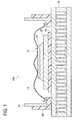
- a power module 100 of this embodiment includes, as shown in FIG 1 , a semiconductor element 10 which is a heat generating element, a metal layer 20 on which the semiconductor element 10 is mounted, a cooler 30 internally formed with coolant flow passages, an insulating resin sheet 40 that insulates the metal layer 20 and the cooler 30 from each other and joins them to each other, and a bus bar housing 60 fixed on the cooler 30 and holding a bus bar 61.
- the power module 100 is configured to dissipate the heat generated in the semiconductor element 10 to the cooler 30 through the metal layer 20 and the insulating resin sheet 40.
- the power module 100 is assembled as shown in FIG 1 such that the insulating resin sheet 40, the metal layer 20, and the semiconductor element 10 are laminated on the cooler 30.
- this lamination direction is referred to as a height direction
- the semiconductor element 10 side in the height direction is referred to as an upper side
- the cooler 30 side in the height direction is referred to as a lower side.
- the semiconductor element 10 is a device such as IGBT constituting an inverter circuit and is electrically connected to the bus bar 61 in the bus bar housing 60 with bonding wires 13.
- the semiconductor element 10 is mounted on the metal layer 20 and fixed thereto with solder 15. It is to be noted that a vehicle-mounted power module mounts thereon many semiconductor elements, but it is schematically illustrated in the present description to simplify the explanation.
- the metal layer 20 is a board on which the semiconductor element 10 is mounted.
- the metal layer 20 serves as an electrode and also as a heat dissipating plate to dissipate the heat from the semiconductor element 10.
- the metal layer 20 is made of a material having high thermal conductivity and high electric conductivity.
- the metal layer 20 is made of copper (Cu) having a thickness of 2 mm to 3 mm.
- the insulating resin sheet 40 is a joining sheet for bonding the cooler 30 and the metal layer 20 together. Further, the insulating resin sheet 40 also has a function to electrically insulate the cooler 30 and the metal layer 20 from each other. As the insulating resin sheet 40, therefore, a sheet having a joining function and an insulating function is used. In the present embodiment, the insulating resin sheet 40 is made of epoxy-system thermosetting resin with a thickness of about 200 ⁇ m.
- the cooler 30 has cooling fins each of which is formed of a rolled sheet shaped in wave form, and a top plate and a bottom plate that fix the cooling fins interposed therebetween.
- Each component constituting the cooler 30 is made of aluminum (Al) having high thermal conductivity and light weight.
- a hollow area defined by the top plate, the bottom plate, and the cooling fins provides flow passages for coolant.
- the coolant may be selected from liquid and gas.
- the components constituting the cooler 30 are integrally joined together with a brazing material in order to efficiently transfer the heat from the semiconductor element 10 to the cooler 30.
- Available brazing materials are aluminum brazing materials such as Al-Si alloy and Al-Si-Mg alloy.
- the cooler 30 configured as above is one example and not limited thereto.
- a coefficient of linear expansion of the metal layer 20 made of copper is about 17 ⁇ 10 -6 /K and a coefficient of linear expansion of the cooler 30 made of aluminum is about 24 ⁇ 10 -6 /K.
- coefficient of linear expansion coefficient of thermal expansion
- a reflow furnace 200 in the present embodiment includes, as shown in FIG 2 , a heating chamber 201 to accommodate a work 1, a radiation-heating type heater 202 placed in an upper side in the heating chamber 201 and configured to emit radiation to heat the work 1, a hot plate 203 located in a lower side in the heating chamber 201 to hold thereon the work 1 and heat the work 1, shielding plates 204 and 205 to block the passage of radiation from the heater 202, and an air blow gun 206 configured to inject cooling air in the heating chamber 201.
- the work 1 in the present embodiment corresponds to the power module 100 to which the semiconductor element 10 is not yet soldered.
- the work 1 is in a state where the semiconductor element 10 is placed on cream solder printed on the metal layer 20.
- the metal layer 20 and the cooler 30 are bonded together through the insulating resin sheet 40.
- the work 1 is placed on the hot plate 203.
- the work 1 is heated from below.
- the work 1 is placed below the heater 202 and thus heated from above by the radiation from the heater 202.
- the reflow furnace 200 is configured to heat the work 1 from both sides, above and below, in the height direction.
- the shielding plates 204 and 205 are movably provided in the heating chamber 201.
- the shielding plate 204 covers upper surfaces (especially, exposed portions) of the cooler 30 and the insulating resin sheet 40 and the shielding plate 205 covers an upper surface of the semiconductor element 10.
- the shielding plates 204 and 205 cover other portions than the metal layer 20 of the work 1 when seen from above in the height direction of the work 1.
- the shielding plates 204 and 205 may be made of any materials capable of reflecting the radiation form the heater 202 to restrain the passage of radiation.
- the plates 204 and 205 are steel plates whose surfaces coated with Au plating.
- the shielding plate 204 includes, as shown in FIG 2 , a shielding part 214 for covering the upper surface of the cooler 30 and a shielding part 224 for covering the upper surface of the insulating resin sheet 40.
- the shielding plate 204 is formed in a shape including the shielding parts 214 and 224 integrally.
- the shielding part 214 and the shielding part 224 of the shielding plate 204 may be provided as separate parts.
- the shielding plates 204 and 205 may consist of a plurality of parts which are assembled to cover necessary portions of the work 1 or may be formed of a single plate having a cutout(s) corresponding to an uncovered portion(s) (the metal layer 20 in this embodiment) of a work.
- the air blow gun 206 is movably provided in the heating chamber 201. This gun 206 injects cooling air toward a portion or portions difficult to be covered by the shielding plate 204 of the cooler 30, thereby cooling the surface of the cooler 30. In the case where it is unnecessary to cool the cooler 30 by use of the air blow gun 206 (e.g., in the case where temperature control mentioned later is enabled by using only the shielding plates 204 and 205), the air blow gun 206 is held outside the heating chamber 201.
- the work 1 is first put on the hot plate 203 as shown in FIG 2 . Further, the shielding plates 204 and 205 are moved to between the work 1 and the heater 202. To be concrete, the shielding plate 204 is placed to cover the upper surfaces of the cooler 30 and the insulating resin sheet 40, while the shielding plate 205 is placed to cover the upper surface of the semiconductor element 10.
- the metal layer 20 is heated to at least a melting temperature of the solder 15.
- the metal layer 20 uncovered with the shielding plates 204 and 205 absorbs the radiation from the heater 202. Accordingly, the metal layer 20 is heated by the heater 202. As the metal layer 20 is heated, the heat is transferred to the solder 15, and thus the solder 15 is melted.
- the cooler 30 and the insulating resin sheet 40 each being covered by the shielding plate 204 hardly absorb the radiation from the heater 202.
- the cooler 30 and the insulating resin sheet 40 are not influenced by the radiation from the heater 202.
- the semiconductor element 10 covered by the shielding plate 205 is little influenced by the radiation from the heater 202.
- the cooler 30 is heated by the hot plate 203.
- heating control of the hot plate 203 is performed so that a thermal expansion amount (i.e., an expanding amount in a width direction) of the cooler 30 is approximately equal to that of the metal layer 20.
- soldering is to be performed at 300°C
- the work 1 is heated by the radiation from the heater 202 so that the temperature of the metal layer 20 reaches 300°C, while the cooler 30 side is controlled so that the temperature of the cooler 30 becomes 212°C.
- the hot plate 203 is controlled to maintain a difference in thermal expansion amount between the metal layer 20 and the cooler 30 within a predetermined value.
- a difference in temperature is provided between the metal layer 20 and the cooler 30 so that the difference in thermal expansion amount between the metal layer 20 and the cooler 30 is a threshold value or less. Since the control is performed to prevent the occurrence of a difference in thermal expansion amount between the metal layer 20 and the cooler 30, the insulating resin sheet 40 is less likely to be deformed or warped and hence stress concentration is restrained.
- the temperature of the cooler 30 is adjusted simply by heating control of the hot plate 203.
- the air blow gun 206 may be used to blow cooling air to the cooler 30 for the purpose of fine adjustment of the temperature of the cooler 30.
- the cooler 30 may be cooled by cooling air to provide a temperature difference between the metal layer 20 and the cooler 30.
- FIG 3 shows a relationship between temperature and coefficient of thermal expansion of a subject to be heated.
- both the temperature of the metal layer 20 and the temperature of the cooler 30 are increased to the melting temperature (a sign A in FIG 3 ) of the solder 15. That is, the temperature of the metal layer 20 and the temperature of the cooler 30 are equal to each other. Accordingly, a difference in thermal expansion amount occurs due to the difference in coefficient of thermal expansion as indicated by a sign D in FIG 3 . This causes peeling of the insulating resin sheet 40.
- the temperature of the metal layer 20 and the temperature of the cooler 30 are controlled to be different from each other so that their thermal expansion amounts are equal to each other.
- the coefficient of thermal expansion of the cooler 30 is higher than that of the metal layer 20. Therefore, the temperature of the cooler 30 is made lower than the metal layer 20 so that the thermal expansion amount of the cooler 30 is equal to the metal layer 20.
- the thermal expansion amounts are equal as above, so that the insulating resin sheet 40 is less warped. This can consequently prevent peeling of the insulating resin sheet 40.
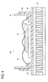
- a power module 110 in a second embodiment is configured, as shown in FIG 4 , such that a shielding film 50 covers a portion of a surface of the cooler 30 facing to the semiconductor element 10, the portion being in noncontact with the insulating resin sheet 40.
- the bus bar housing 60 is fixed onto the shielding film 50.
- the shielding film 50 reflects the radiation from the heater 202 to restrain the passage of radiation.
- an Au film is usable.
- the shielding film 50 has a function similar to the shielding plates 204 and 205 of the reflow furnace 200. Further, the shielding film 50 is in noncontact with the metal layer 20 and electrically insulated from the metal layer 20 by the insulating resin sheet 40.
- the surface of the cooler 30 facing to the heater 202 is covered by the shielding film 50.
- the heater 202 does not contribute to heating of the cooler 30. Accordingly, in a similar manner to the first embodiment, a temperature difference can be provided between the metal layer 20 and the cooler 30.
- the power module 110 is provided in itself with a shielding member, any shielding plate does not need to be provided in the reflow furnace as disclosed in the first embodiment. Even when the configuration of the power module is changed, therefore, there is no need to change the configuration of the reflow furnace. Therefore, the reflow furnace has a simpler configuration than that in the first embodiment.
- the power module does not need any shielding film.
- the number of components of the power module can be small. Further, manufacturing of such cooler needs no step of covering the cooler by the shielding film and the cooler can be made simpler than that in the second embodiment.
- the work 1 is heated so that the metal layer 20 (a low thermal expansion member) becomes higher in temperature as compared with the cooler 30 (a high thermal expansion member).
- the metal layer 20 is heated to a melting temperature of the solder 15 and the cooler 30 is heated to have a thermal expansion amount approximately equal to the thermal expansion amount of the metal layer 20. Since the metal layer 20 and the cooler 30 are heated as above to different temperatures, their thermal expansion amounts are little different from each other as compared with the case where the metal layer 20 and the cooler 30 are heated to almost the same temperature. Accordingly, shear stress generated in the insulating resin sheet 40 is small and thus it can be expected to prevent peeling of the insulating resin sheet 40.
- the radiation-heating type heater 202 and the hot plate 203 are used as heating devices for heating the work 1 in the above embodiments, the invention is not limited thereto.
- the work 1 may be heated by heated air, laser heating, arc heating, electromagnetic induction heating, electronic beam heating, or ion beam heating.
- the cooling air from the air blow gun 206 is used as a cooling device for cooling the work 1, but the invention is not limited thereto.
- the work 1 may be cooled by a cooling plate, cooling water, or compression cooling.
- the sheet-like member 40 is used as a member for joining the metal layer 20 and the cooler 30 and insulating them from each other.
- a plate-like member (a ceramic insulating plate, etc.) may be used.
- heating of the metal layer 20 and the cooler 30 is controlled so that the temperature of the cooler 30 is lower than the temperature of the metal layer 20.
- the invention is not limited to such heating control.
- heating is controlled so that the temperature of the cooler 30 is higher than that of the metal layer 20, thereby making their thermal expansion amounts equal to each other.
Landscapes
- Engineering & Computer Science (AREA)
- Mechanical Engineering (AREA)
- Physics & Mathematics (AREA)
- Plasma & Fusion (AREA)
- Optics & Photonics (AREA)
- Cooling Or The Like Of Semiconductors Or Solid State Devices (AREA)
- Cooling Or The Like Of Electrical Apparatus (AREA)
- Die Bonding (AREA)
Abstract
Description
- The present invention relates to a semiconductor module in which an electrode layer that mounts thereon a semiconductor element and a cooler are assembled together by interposing an insulating joining layer therebetween, and a manufacturing method of the semiconductor module. More specifically, the present invention relates to a manufacturing method and a manufacturing device for a semiconductor module to reduce peeling of an insulating joining layer.
- A high-pressure-resistant and large-current power module to be mounted in a hybrid electric vehicle, an electric vehicle, etc. provides a large self-heating value or amount during operation of a semiconductor element. Accordingly, such a vehicle-mounted power module has to include a cooling structure having high heat dissipation performance.
- As the power module including the cooling structure, for example, there is known a configuration that an insulating resin sheet, a metal layer serving as an electrode, and a semiconductor element are laminated on a cooler having coolant flow passages. The semiconductor element is fixed to the metal layer with solder, and the metal layer and the cooler are joined through the insulating resin sheet. This power module is configured to efficiently release the heat generated from the semiconductor element by the cooler through the metal layer which is superior in thermal conductivity and the thin-layer insulating resin sheet.
- As a device to solder an electronic component onto an electronic circuit board, for example, Patent Document 1 discloses a reflow device for mounting an electronic component onto an electronic circuit board by heating, melting, and then cooling solder. Patent Document 1 describes that this reflow device is arranged so that a heat shielding member having a plurality of openings is interposed between a far-infrared heater and a subject to be processed to partially adjust a heating temperature in the surface of the electronic circuit board.
- Patent Document 1:
JP2003-332727A - However, the aforementioned conventional semiconductor modules have the following disadvantages. Specifically, since the metal layer and the cooler have a difference in coefficient of thermal expansion (coefficient of linear expansion), the insulating resin sheet is apt to peel off due to such a difference in coefficient of thermal expansion.
- For instance, in the case where the metal layer is made of copper and the cooler is made of aluminum in the aforementioned conventional power module, in which the copper has a coefficient of linear expansion of about 17 × 10-6/K and the aluminum has a coefficient of linear expansion of about 24 × 10-6/K, a difference in thermal expansion amount is generated in a high-temperature environment where soldering is performed. Thus, shear stress occurs in the insulating resin sheet, causing peeling of the insulating resin sheet. This peeling could be caused even when the heating temperature in the surface of the electronic circuit board is partially adjusted as in the reflow device shown in Patent Document 1. Gaps generated due to the peeling may decrease the joint area between the insulating resin sheet serving as an insulating joining layer and the metal layer (or the cooler), thereby lowering a heat dissipation performance of the power module.
- The present invention has been made to solve the aforementioned problems of the conventional semiconductor modules and has a purpose to provide a method of manufacturing a semiconductor module to reduce stress concentration in an insulating joining layer and prevent an insulating resin layer from peeling off.
- To achieve the above purpose, one aspect of the invention provides a method of manufacturing a semiconductor module, the module including: a semiconductor element: a metal layer on which the semiconductor element is mounted; a cooler consisting of a material having a coefficient of thermal expansion different from a coefficient of thermal expansion of the metal layer; and an insulating joining layer joining the metal layer and the cooler to each other and electrically insulating the metal layer and the cooler from each other, wherein the method includes a mounting process of heating a subject to be heated in which the metal layer and the cooler are joined integrally through the insulating joining layer and the semiconductor element is placed on the metal layer through solder, so that one of the metal layer and the cooler, corresponding to a low thermal expansion member having a lower coefficient of thermal expansion, is higher in temperature than the other corresponding to a high thermal expansion member having a higher coefficient of thermal expansion.
- The above semiconductor module manufacturing method is achieved by preparing a subject to be heated (a work) in which the metal layer and the cooler, which have different coefficients of thermal expansion (coefficients of linear expansion) from each other, are joined together through the insulating joining layer, and the semiconductor element is mounted on the metal layer with solder. The subject is heated to melt the solder, thereby joining the semiconductor element on the metal layer. During the heating of the subject, assuming that one of the metal layer and the cooling part, the one having a lower coefficient of thermal expansion, is a low thermal expansion member and the other having a higher coefficient of thermal expansion is a high thermal expansion member, the subject is heated so that the temperature of the low thermal expansion member becomes higher than that of the high thermal expansion member. To be concrete, the metal layer is heated to a melting temperature of the solder, and the cooler is heated so that the thermal expansion amount of the cooler becomes approximately equal to that of the metal layer. Specifically, if the cooler is the high thermal expansion member, the cooler is heated to a lower temperature than the metal layer. On the other hand, if the cooler is the low thermal expansion member, the cooler is heated to a higher temperature than the metal layer.
- In the above semiconductor module manufacturing method, he metal layer and the cooler are heated to different temperatures from each other so that their thermal expansion amounts are equal to each other. According to this method, it can be expected to reduce shear stress occurring in the insulating joining layer as compared with the conventional case where the metal layer and the cooler are heated to an almost equal temperature. It is therefore expected to prevent the insulating joining layer from peeling.
- The above mounting process preferably includes heating the subject from both sides in a height direction of the subject by a first heating member for heating the subject from above and a second heating member for heating subject from below, and controlling at least one of the first heating member and the second heating member so that the thermal expansion amount of the high thermal expansion member and the thermal expansion amount of the low thermal expansion member are approximately equal to each other. When the subject is heated from both sides in a height direction of the subject and the temperature of at least one of the heating members is controlled, the temperature difference can be provided with high precision.
- The above mounting process preferably includes heating the subject from a semiconductor element side in the height direction of the subject by a radiation-heating type heating device, and holding a shielding member on at least a surface of the cooler facing to the semiconductor element to shield radiation from the heating device while the heating device heats the subject. As this configuration, when an upper surface (an exposed portion) of the cooler is covered by the shielding member to restrict heating of the cooler, the temperature difference between the cooler and the metal layer is easily provided.
- Preferably, the mounting process includes heating the subject while cooling the high thermal expansion member. For the cooling device, for example, an air blow or a cooling plate is available. Since the high thermal expansion member is cooled by such a cooling device, the temperature difference is more easily provided.
- Another aspect of the invention provides a semiconductor module including: a semiconductor element; a metal layer on which the semiconductor element is mounted; a cooler consisting of a material having a coefficient of thermal expansion different from a coefficient of thermal expansion of the metal layer; and an insulating joining layer joining the metal layer and the cooler to each other and electrically insulating the metal layer and the cooler from each other; and a shielding film electrically insulated from the metal layer and provided to cover a surface of the cooler facing to the semiconductor element to shield radiation.
- Still another aspect of the invention provides a device for manufacturing a semiconductor module, the module including: a semiconductor element; a metal layer on which the semiconductor element is mounted; a cooler consisting of a material having a coefficient of thermal expansion different from a coefficient of thermal expansion of the metal layer; and an insulating joining layer joining the metal layer and the cooler to each other and electrically insulating the metal layer and the cooler from each other, wherein the device includes: a heating chamber for accommodating a subject to be heated, the subject being configured such that the metal layer and the cooler are integrally joined through the insulating joining layer and the semiconductor element is placed on the metal layer with solder, and a heating device for heating the subject so that a temperature of one of the metal layer and the cooler, corresponding to a low thermal expansion member having a lower coefficient of thermal expansion, is higher than the other corresponding to a temperature of a high thermal expansion member having a higher coefficient of thermal expansion.
- According to the invention, a method of manufacturing a semiconductor module can be achieved capable of reducing stress concentration in an insulating joining layer and preventing peeling of the insulating joining layer.
-
-
FIG 1 is a configuration view of a power module in an embodiment; -
FIG 2 is a configuration view of a reflow furnace in the embodiment; -
FIG 3 is a graph showing a relationship between temperature and thermal expansion amount of a subject to be heated; and -
FIG 4 is a configuration view of a power module in a modified example. - A detailed description of a preferred embodiment of the present invention will now be given referring to the accompanying drawings. In the following explanation, the invention is applied to an intelligent power module for hybrid vehicle.
- A
power module 100 of this embodiment includes, as shown inFIG 1 , asemiconductor element 10 which is a heat generating element, ametal layer 20 on which thesemiconductor element 10 is mounted, acooler 30 internally formed with coolant flow passages, aninsulating resin sheet 40 that insulates themetal layer 20 and thecooler 30 from each other and joins them to each other, and abus bar housing 60 fixed on thecooler 30 and holding abus bar 61. Thepower module 100 is configured to dissipate the heat generated in thesemiconductor element 10 to thecooler 30 through themetal layer 20 and theinsulating resin sheet 40. - The
power module 100 is assembled as shown inFIG 1 such that theinsulating resin sheet 40, themetal layer 20, and thesemiconductor element 10 are laminated on thecooler 30. In this description, this lamination direction is referred to as a height direction, thesemiconductor element 10 side in the height direction is referred to as an upper side, and thecooler 30 side in the height direction is referred to as a lower side. - The
semiconductor element 10 is a device such as IGBT constituting an inverter circuit and is electrically connected to thebus bar 61 in thebus bar housing 60 withbonding wires 13. Thesemiconductor element 10 is mounted on themetal layer 20 and fixed thereto withsolder 15. It is to be noted that a vehicle-mounted power module mounts thereon many semiconductor elements, but it is schematically illustrated in the present description to simplify the explanation. - The
metal layer 20 is a board on which thesemiconductor element 10 is mounted. Themetal layer 20 serves as an electrode and also as a heat dissipating plate to dissipate the heat from thesemiconductor element 10. Accordingly, themetal layer 20 is made of a material having high thermal conductivity and high electric conductivity. In the present embodiment, themetal layer 20 is made of copper (Cu) having a thickness of 2 mm to 3 mm. - The
insulating resin sheet 40 is a joining sheet for bonding thecooler 30 and themetal layer 20 together. Further, theinsulating resin sheet 40 also has a function to electrically insulate thecooler 30 and themetal layer 20 from each other. As the insulatingresin sheet 40, therefore, a sheet having a joining function and an insulating function is used. In the present embodiment, the insulatingresin sheet 40 is made of epoxy-system thermosetting resin with a thickness of about 200 µm. - The cooler 30 has cooling fins each of which is formed of a rolled sheet shaped in wave form, and a top plate and a bottom plate that fix the cooling fins interposed therebetween. Each component constituting the cooler 30 is made of aluminum (Al) having high thermal conductivity and light weight. A hollow area defined by the top plate, the bottom plate, and the cooling fins provides flow passages for coolant. The coolant may be selected from liquid and gas. The components constituting the cooler 30 are integrally joined together with a brazing material in order to efficiently transfer the heat from the
semiconductor element 10 to the cooler 30. Available brazing materials are aluminum brazing materials such as Al-Si alloy and Al-Si-Mg alloy. The cooler 30 configured as above is one example and not limited thereto. - In the present embodiment, a coefficient of linear expansion of the
metal layer 20 made of copper is about 17 × 10-6/K and a coefficient of linear expansion of the cooler 30 made of aluminum is about 24 × 10-6/K. Thus, there is a difference in coefficient of linear expansion (coefficient of thermal expansion) between themetal layer 20 and the cooler 30. The cooler 30 is easier to expand than themetal layer 20. - The reflow furnace for mounting the
semiconductor element 10 of thepower module 100 will be explained below. Areflow furnace 200 in the present embodiment includes, as shown inFIG 2 , aheating chamber 201 to accommodate a work 1, a radiation-heating type heater 202 placed in an upper side in theheating chamber 201 and configured to emit radiation to heat the work 1, ahot plate 203 located in a lower side in theheating chamber 201 to hold thereon the work 1 and heat the work 1, shieldingplates heater 202, and anair blow gun 206 configured to inject cooling air in theheating chamber 201. - The work 1 in the present embodiment corresponds to the
power module 100 to which thesemiconductor element 10 is not yet soldered. In other words, for example, the work 1 is in a state where thesemiconductor element 10 is placed on cream solder printed on themetal layer 20. In the work 1, themetal layer 20 and the cooler 30 are bonded together through the insulatingresin sheet 40. - In the
reflow furnace 200, as shown inFIG 2 , the work 1 is placed on thehot plate 203. By the heat from thehot plate 203, the work 1 is heated from below. Further, the work 1 is placed below theheater 202 and thus heated from above by the radiation from theheater 202. In other words, thereflow furnace 200 is configured to heat the work 1 from both sides, above and below, in the height direction. - The shielding
plates heating chamber 201. During heating of the work 1, the shieldingplate 204 covers upper surfaces (especially, exposed portions) of the cooler 30 and the insulatingresin sheet 40 and theshielding plate 205 covers an upper surface of thesemiconductor element 10. Specifically, the shieldingplates metal layer 20 of the work 1 when seen from above in the height direction of the work 1. The shieldingplates heater 202 to restrain the passage of radiation. In the present embodiment, theplates - The shielding
plate 204 includes, as shown inFIG 2 , a shieldingpart 214 for covering the upper surface of the cooler 30 and a shieldingpart 224 for covering the upper surface of the insulatingresin sheet 40. The shieldingplate 204 is formed in a shape including the shieldingparts - The shielding
part 214 and the shieldingpart 224 of theshielding plate 204 may be provided as separate parts. For instance, the shieldingplates metal layer 20 in this embodiment) of a work. - The
air blow gun 206 is movably provided in theheating chamber 201. Thisgun 206 injects cooling air toward a portion or portions difficult to be covered by the shieldingplate 204 of the cooler 30, thereby cooling the surface of the cooler 30. In the case where it is unnecessary to cool the cooler 30 by use of the air blow gun 206 (e.g., in the case where temperature control mentioned later is enabled by using only the shieldingplates 204 and 205), theair blow gun 206 is held outside theheating chamber 201. - A soldering procedure in the
power module 100 by use of theaforementioned reflow furnace 200 will be explained below. - The work 1 is first put on the
hot plate 203 as shown inFIG 2 . Further, the shieldingplates heater 202. To be concrete, the shieldingplate 204 is placed to cover the upper surfaces of the cooler 30 and the insulatingresin sheet 40, while theshielding plate 205 is placed to cover the upper surface of thesemiconductor element 10. - Subsequently, heating using the
heater 202 and thehot plate 203 is started. Specifically, themetal layer 20 is heated to at least a melting temperature of thesolder 15. At that time, themetal layer 20 uncovered with the shieldingplates heater 202. Accordingly, themetal layer 20 is heated by theheater 202. As themetal layer 20 is heated, the heat is transferred to thesolder 15, and thus thesolder 15 is melted. - The cooler 30 and the insulating
resin sheet 40 each being covered by the shieldingplate 204 hardly absorb the radiation from theheater 202. Thus, the cooler 30 and the insulatingresin sheet 40 are not influenced by the radiation from theheater 202. Similarly, thesemiconductor element 10 covered by the shieldingplate 205 is little influenced by the radiation from theheater 202. - In the cooler 30 side, on the other hand, the cooler 30 is heated by the
hot plate 203. In thereflow furnace 200, concretely, heating control of thehot plate 203 is performed so that a thermal expansion amount (i.e., an expanding amount in a width direction) of the cooler 30 is approximately equal to that of themetal layer 20. When soldering is to be performed at 300°C, the work 1 is heated by the radiation from theheater 202 so that the temperature of themetal layer 20 reaches 300°C, while the cooler 30 side is controlled so that the temperature of the cooler 30 becomes 212°C. While the work 1 is heated by theheater 202 and thehot plate 203, the temperature of themetal layer 20 and the temperature of the cooler 30 are continuously detected and the temperature of the cooler 30 is increased following the increasing temperature of themetal layer 20 so that their thermal expansion amounts are approximately equal to each other. Specifically, thehot plate 203 is controlled to maintain a difference in thermal expansion amount between themetal layer 20 and the cooler 30 within a predetermined value. - In this reflow process (one example of the mounting process), a difference in temperature is provided between the
metal layer 20 and the cooler 30 so that the difference in thermal expansion amount between themetal layer 20 and the cooler 30 is a threshold value or less. Since the control is performed to prevent the occurrence of a difference in thermal expansion amount between themetal layer 20 and the cooler 30, the insulatingresin sheet 40 is less likely to be deformed or warped and hence stress concentration is restrained. - During adjustment of the temperature of the cooler 30, the temperature of the cooler 30 is adjusted simply by heating control of the
hot plate 203. As an alternative, theair blow gun 206 may be used to blow cooling air to the cooler 30 for the purpose of fine adjustment of the temperature of the cooler 30. As another alternative, instead of using the shieldingplates metal layer 20 and the cooler 30. -
FIG 3 shows a relationship between temperature and coefficient of thermal expansion of a subject to be heated. In the conventional example, both the temperature of themetal layer 20 and the temperature of the cooler 30 are increased to the melting temperature (a sign A inFIG 3 ) of thesolder 15. That is, the temperature of themetal layer 20 and the temperature of the cooler 30 are equal to each other. Accordingly, a difference in thermal expansion amount occurs due to the difference in coefficient of thermal expansion as indicated by a sign D inFIG 3 . This causes peeling of the insulatingresin sheet 40. - In the present embodiment, in contrast, the temperature of the
metal layer 20 and the temperature of the cooler 30 are controlled to be different from each other so that their thermal expansion amounts are equal to each other. In the present embodiment, specifically, the coefficient of thermal expansion of the cooler 30 is higher than that of themetal layer 20. Therefore, the temperature of the cooler 30 is made lower than themetal layer 20 so that the thermal expansion amount of the cooler 30 is equal to themetal layer 20. For instance, when themetal layer 20 reaches the temperature A inFIG 3 , the temperature of the cooler 30 is adjusted to a temperature B at which the thermal expansion amount of the cooler 30 becomes equal to a thermal expansion amount C of the metal layer A. In the present embodiment, the thermal expansion amounts are equal as above, so that the insulatingresin sheet 40 is less warped. This can consequently prevent peeling of the insulatingresin sheet 40. - A
power module 110 in a second embodiment is configured, as shown inFIG 4 , such that a shieldingfilm 50 covers a portion of a surface of the cooler 30 facing to thesemiconductor element 10, the portion being in noncontact with the insulatingresin sheet 40. Thebus bar housing 60 is fixed onto the shieldingfilm 50. - The shielding
film 50 reflects the radiation from theheater 202 to restrain the passage of radiation. For example, an Au film is usable. Specifically, the shieldingfilm 50 has a function similar to the shieldingplates reflow furnace 200. Further, the shieldingfilm 50 is in noncontact with themetal layer 20 and electrically insulated from themetal layer 20 by the insulatingresin sheet 40. - In the
power module 110, the surface of the cooler 30 facing to theheater 202 is covered by the shieldingfilm 50. Thus, theheater 202 does not contribute to heating of the cooler 30. Accordingly, in a similar manner to the first embodiment, a temperature difference can be provided between themetal layer 20 and the cooler 30. - Since the
power module 110 is provided in itself with a shielding member, any shielding plate does not need to be provided in the reflow furnace as disclosed in the first embodiment. Even when the configuration of the power module is changed, therefore, there is no need to change the configuration of the reflow furnace. Therefore, the reflow furnace has a simpler configuration than that in the first embodiment. - On the other hand, in the case where the shielding plate is provided in the reflow furnace as in the first embodiment, the power module does not need any shielding film. Thus, the number of components of the power module can be small. Further, manufacturing of such cooler needs no step of covering the cooler by the shielding film and the cooler can be made simpler than that in the second embodiment.
- As explained in detail above, in the soldering process of the power module in the present embodiments, the work 1 is heated so that the metal layer 20 (a low thermal expansion member) becomes higher in temperature as compared with the cooler 30 (a high thermal expansion member). Specifically, the
metal layer 20 is heated to a melting temperature of thesolder 15 and the cooler 30 is heated to have a thermal expansion amount approximately equal to the thermal expansion amount of themetal layer 20. Since themetal layer 20 and the cooler 30 are heated as above to different temperatures, their thermal expansion amounts are little different from each other as compared with the case where themetal layer 20 and the cooler 30 are heated to almost the same temperature. Accordingly, shear stress generated in the insulatingresin sheet 40 is small and thus it can be expected to prevent peeling of the insulatingresin sheet 40. - The above embodiments are mere examples and do not give any limitations to the present invention. The present invention therefore may be embodied in other specific forms without departing from the essential characteristics thereof. For instance, although the above embodiments show that the present invention is applied to the intelligent power module for hybrid vehicle, the invention is also applicable to general modules including electronic components mounted on electronic circuit boards.
- Although the radiation-
heating type heater 202 and thehot plate 203 are used as heating devices for heating the work 1 in the above embodiments, the invention is not limited thereto. For instance, the work 1 may be heated by heated air, laser heating, arc heating, electromagnetic induction heating, electronic beam heating, or ion beam heating. - In the above embodiments, the cooling air from the
air blow gun 206 is used as a cooling device for cooling the work 1, but the invention is not limited thereto. For instance, the work 1 may be cooled by a cooling plate, cooling water, or compression cooling. - In the above embodiments, the sheet-
like member 40 is used as a member for joining themetal layer 20 and the cooler 30 and insulating them from each other. Instead of such a sheet-like member, a plate-like member (a ceramic insulating plate, etc.) may be used. - In the above embodiments, on ground that the coefficient of thermal expansion of the cooler 30 is higher than that of the
metal layer 20, heating of themetal layer 20 and the cooler 30 is controlled so that the temperature of the cooler 30 is lower than the temperature of themetal layer 20. However, the invention is not limited to such heating control. In the case where the coefficient of thermal expansion of the cooler 30 is lower than that of themetal layer 20, heating is controlled so that the temperature of the cooler 30 is higher than that of themetal layer 20, thereby making their thermal expansion amounts equal to each other. -
- 1
- Work (Subject to be heated)
- 10
- Semiconductor element
- 15
- Solder
- 20
- Metal layer
- 30
- Cooler
- 40
- Insulating resin sheet (Insulating joining layer)
- 100
- Power module (Semiconductor module)
- 200
- Reflow furnace
- 201
- Heating chamber
- 202
- Radiation-heating type heater
- 203
- Hot plate
- 204
- Shielding plate
Claims (11)
- A method of manufacturing a semiconductor module, the module including:a semiconductor element:a metal layer on which the semiconductor element is mounted;a cooler consisting of a material having a coefficient of thermal expansion different from a coefficient of thermal expansion of the metal layer; andan insulating joining layer joining the metal layer and the cooler to each other and electrically insulating the metal layer and the cooler from each other,wherein the method includes a mounting process of heating a subject to be heated in which the metal layer and the cooler are joined integrally through the insulating joining layer and the semiconductor element is placed on the metal layer through solder, so that one of the metal layer and the cooler, corresponding to a low thermal expansion member having a lower coefficient of thermal expansion, is higher in temperature than the other corresponding to a high thermal expansion member having a higher coefficient of thermal expansion.
- The method of manufacturing a semiconductor module according to claim 1, wherein the mounting process includes heating the metal layer to a melting temperature of the solder and heating the cooler so that a thermal expansion amount of the cooler is approximately equal to a thermal expansion amount of the metal layer.
- The method of manufacturing a semiconductor module according to claim 1 or 2, wherein the mounting process includes heating the subject from both sides in a height direction of the subject by a first heating member for heating the subject from above and a second heating member for heating subject from below, and controlling at least one of the first heating member and the second heating member so that the thermal expansion amount of the high thermal expansion member and the thermal expansion amount of the low thermal expansion member are approximately equal to each other.
- The method of manufacturing a semiconductor module according to any one of claims 1 to 3, wherein the mounting process heating the subject from a semiconductor element side in the height direction of the subject by a radiation-heating type heating device, and holding a shielding member on at least a surface of the cooler facing to the semiconductor element to shield radiation from the heating device while the heating device heats the subject.
- The method of manufacturing a semiconductor module according to any one of claims 1 to 4, wherein the mounting process includes heating the subject while cooling the high thermal expansion member.
- A semiconductor module including:a semiconductor element;a metal layer on which the semiconductor element is mounted;a cooler consisting of a material having a coefficient of thermal expansion different from a coefficient of thermal expansion of the metal layer; andan insulating joining layer joining the metal layer and the cooler to each other and electrically insulating the metal layer and the cooler from each other; anda shielding film electrically insulated from the metal layer and provided to cover a surface of the cooler facing to the semiconductor element to shield radiation.
- A device for manufacturing a semiconductor module, the module including:a semiconductor element;a metal layer on which the semiconductor element is mounted;a cooler consisting of a material having a coefficient of thermal expansion different from a coefficient of thermal expansion of the metal layer; andan insulating joining layer joining the metal layer and the cooler to each other and electrically insulating the metal layer and the cooler from each other,wherein the device includes:a heating chamber for accommodating a subject to be heated, the subject being configured such that the metal layer and the cooler are integrally joined through the insulating joining layer and the semiconductor element is placed on the metal layer with solder, anda heating device for heating the subject so that a temperature of one of the metal layer and the cooler, corresponding to a low thermal expansion member having a lower coefficient of thermal expansion, is higher than the other corresponding to a temperature of a high thermal expansion member having a higher coefficient of thermal expansion.
- The device for manufacturing a semiconductor module according to claim 7, wherein the heating device heats the metal layer to a melting temperature of the solder and heats the cooler so that a thermal expansion amount of the cooler is approximately equal to a thermal expansion amount of the metal layer.
- The device for manufacturing a semiconductor module according to claim 7 or 8, wherein the heating device includes:a first heating member for heating the subject from above in a height direction of the subject; anda second heating member for heating the subject from below in the height direction of the subject,wherein at least one of the first heating member and the second heating member is controlled so that a thermal expansion amount of the high thermal expansion member and a thermal expansion amount of the low thermal expansion member are approximately equal to each other.
- The device for manufacturing a semiconductor module according to any one of claims 7 to 9, wherein
the heating device is a radiation-heating type heating device for heating the subject from a semiconductor element side in the height direction of the subject,
the device includes a shielding member for shielding radiation from the heating device, and
the shielding member is placed on at least a surface of the cooler facing to the semiconductor element while the heating device heats the subject. - The device for manufacturing a semiconductor module according to any one of claims 7 to 10 further including a cooling device for cooling the high thermal expansion member.
Applications Claiming Priority (1)
| Application Number | Priority Date | Filing Date | Title |
|---|---|---|---|
| PCT/JP2010/052810 WO2011104826A1 (en) | 2010-02-24 | 2010-02-24 | Semiconductor module manufacturing method, semiconductor module, and manufacturing device |
Publications (2)
| Publication Number | Publication Date |
|---|---|
| EP2541594A1 true EP2541594A1 (en) | 2013-01-02 |
| EP2541594A4 EP2541594A4 (en) | 2016-12-07 |
Family
ID=44506273
Family Applications (1)
| Application Number | Title | Priority Date | Filing Date |
|---|---|---|---|
| EP10846493.4A Withdrawn EP2541594A4 (en) | 2010-02-24 | 2010-02-24 | SEMICONDUCTOR MODULE MANUFACTURING METHOD, SEMICONDUCTOR MODULE, AND MANUFACTURING DEVICE |
Country Status (5)
| Country | Link |
|---|---|
| US (1) | US8791564B2 (en) |
| EP (1) | EP2541594A4 (en) |
| JP (1) | JP5561356B2 (en) |
| CN (1) | CN102782836B (en) |
| WO (1) | WO2011104826A1 (en) |
Cited By (1)
| Publication number | Priority date | Publication date | Assignee | Title |
|---|---|---|---|---|
| EP4266363A1 (en) * | 2022-04-21 | 2023-10-25 | Airbus SAS | Improved power component for electric or hybrid aircraft |
Families Citing this family (23)
| Publication number | Priority date | Publication date | Assignee | Title |
|---|---|---|---|---|
| US9012766B2 (en) | 2009-11-12 | 2015-04-21 | Silevo, Inc. | Aluminum grid as backside conductor on epitaxial silicon thin film solar cells |
| US9214576B2 (en) | 2010-06-09 | 2015-12-15 | Solarcity Corporation | Transparent conducting oxide for photovoltaic devices |
| US9054256B2 (en) | 2011-06-02 | 2015-06-09 | Solarcity Corporation | Tunneling-junction solar cell with copper grid for concentrated photovoltaic application |
| JP5813137B2 (en) * | 2011-12-26 | 2015-11-17 | 三菱電機株式会社 | Power semiconductor device and manufacturing method thereof |
| US9865754B2 (en) | 2012-10-10 | 2018-01-09 | Tesla, Inc. | Hole collectors for silicon photovoltaic cells |
| US10074755B2 (en) | 2013-01-11 | 2018-09-11 | Tesla, Inc. | High efficiency solar panel |
| US9219174B2 (en) | 2013-01-11 | 2015-12-22 | Solarcity Corporation | Module fabrication of solar cells with low resistivity electrodes |
| US9412884B2 (en) | 2013-01-11 | 2016-08-09 | Solarcity Corporation | Module fabrication of solar cells with low resistivity electrodes |
| US10309012B2 (en) | 2014-07-03 | 2019-06-04 | Tesla, Inc. | Wafer carrier for reducing contamination from carbon particles and outgassing |
| US9296056B2 (en) * | 2014-07-08 | 2016-03-29 | International Business Machines Corporation | Device for thermal management of surface mount devices during reflow soldering |
| US9899546B2 (en) | 2014-12-05 | 2018-02-20 | Tesla, Inc. | Photovoltaic cells with electrodes adapted to house conductive paste |
| US9947822B2 (en) | 2015-02-02 | 2018-04-17 | Tesla, Inc. | Bifacial photovoltaic module using heterojunction solar cells |
| US9761744B2 (en) | 2015-10-22 | 2017-09-12 | Tesla, Inc. | System and method for manufacturing photovoltaic structures with a metal seed layer |
| US9842956B2 (en) | 2015-12-21 | 2017-12-12 | Tesla, Inc. | System and method for mass-production of high-efficiency photovoltaic structures |
| US10115838B2 (en) | 2016-04-19 | 2018-10-30 | Tesla, Inc. | Photovoltaic structures with interlocking busbars |
| CN109983350B (en) * | 2016-11-29 | 2022-02-22 | 东京毅力科创株式会社 | Stages and test equipment for electronic devices |
| US10672919B2 (en) | 2017-09-19 | 2020-06-02 | Tesla, Inc. | Moisture-resistant solar cells for solar roof tiles |
| US11190128B2 (en) | 2018-02-27 | 2021-11-30 | Tesla, Inc. | Parallel-connected solar roof tile modules |
| DE102019206262A1 (en) | 2019-05-02 | 2020-11-05 | Abb Schweiz Ag | Semiconductor component, motor vehicle and method for producing a semiconductor component |
| JP2021011830A (en) * | 2019-07-04 | 2021-02-04 | 本田技研工業株式会社 | How to assemble the pump |
| US11633797B2 (en) * | 2019-11-15 | 2023-04-25 | General Electric Company | Braze joints for a component and methods of forming the same |
| WO2022249234A1 (en) * | 2021-05-24 | 2022-12-01 | 日本電信電話株式会社 | Wavelength conversion device and method for manufacturing wavelength conversion device |
| DE102024205421B3 (en) | 2024-06-12 | 2025-10-30 | Schaeffler Technologies AG & Co. KG | Method for manufacturing an electronic module-cooler assembly, inverter with an electronic module-cooler assembly |
Family Cites Families (13)
| Publication number | Priority date | Publication date | Assignee | Title |
|---|---|---|---|---|
| JPH01272123A (en) * | 1988-04-25 | 1989-10-31 | Fujitsu Ltd | Mounting of semiconductor chip |
| JPH08213724A (en) * | 1995-01-31 | 1996-08-20 | Mitsumi Electric Co Ltd | Circuit board |
| JPH09219582A (en) | 1996-02-09 | 1997-08-19 | Fuji Xerox Co Ltd | Reflow device and its temperature control method |
| JP4272306B2 (en) * | 1999-06-15 | 2009-06-03 | 株式会社タムラ製作所 | Reflow device |
| JP2001358263A (en) * | 2000-06-12 | 2001-12-26 | Hitachi Ltd | Semiconductor device and circuit forming method thereof |
| JP2003332727A (en) | 2002-05-15 | 2003-11-21 | Sony Corp | Heat shielding parts and reflow equipment |
| JP2004146512A (en) * | 2002-10-23 | 2004-05-20 | Toyota Motor Corp | Semiconductor device and method of manufacturing the same |
| CN100468725C (en) * | 2006-07-25 | 2009-03-11 | 威盛电子股份有限公司 | Anti-electrostatic discharge heat dissipation module and system thereof |
| US8030760B2 (en) * | 2006-12-05 | 2011-10-04 | Kabushiki Kaisha Toyota Jidoshokki | Semiconductor apparatus and manufacturing method thereof |
| JP5145715B2 (en) * | 2007-01-12 | 2013-02-20 | 富士電機株式会社 | Semiconductor device and manufacturing method thereof |
| US8169789B1 (en) * | 2007-04-10 | 2012-05-01 | Nvidia Corporation | Graphics processing unit stiffening frame |
| JP2008294280A (en) * | 2007-05-25 | 2008-12-04 | Showa Denko Kk | Semiconductor device |
| JP5103064B2 (en) | 2007-06-19 | 2012-12-19 | 株式会社タムラ製作所 | Reflow device |
-
2010
- 2010-02-24 JP JP2012501565A patent/JP5561356B2/en not_active Expired - Fee Related
- 2010-02-24 US US13/580,754 patent/US8791564B2/en not_active Expired - Fee Related
- 2010-02-24 WO PCT/JP2010/052810 patent/WO2011104826A1/en not_active Ceased
- 2010-02-24 CN CN201080064816.0A patent/CN102782836B/en not_active Expired - Fee Related
- 2010-02-24 EP EP10846493.4A patent/EP2541594A4/en not_active Withdrawn
Cited By (1)
| Publication number | Priority date | Publication date | Assignee | Title |
|---|---|---|---|---|
| EP4266363A1 (en) * | 2022-04-21 | 2023-10-25 | Airbus SAS | Improved power component for electric or hybrid aircraft |
Also Published As
| Publication number | Publication date |
|---|---|
| JPWO2011104826A1 (en) | 2013-06-17 |
| WO2011104826A1 (en) | 2011-09-01 |
| CN102782836B (en) | 2016-03-09 |
| CN102782836A (en) | 2012-11-14 |
| US20120319253A1 (en) | 2012-12-20 |
| JP5561356B2 (en) | 2014-07-30 |
| EP2541594A4 (en) | 2016-12-07 |
| US8791564B2 (en) | 2014-07-29 |
Similar Documents
| Publication | Publication Date | Title |
|---|---|---|
| US8791564B2 (en) | Method of Manufacturing a semiconductor module and device for the same | |
| KR101384426B1 (en) | Base for power module | |
| KR101971756B1 (en) | Substrate for power module, substrate for power module with heat sink, power module, and method for manufacturing substrate for power module | |
| TWI305064B (en) | Thermoelectric module | |
| JP5344888B2 (en) | Semiconductor device | |
| US20150055302A1 (en) | Power module substrate with heatsink, power module substrate with cooler and power module | |
| EP2477223B1 (en) | Method of manufacturing a semiconductor apparatus | |
| CN111448654B (en) | Heat sink for electronic components, electronic assembly having such heat sink and method of manufacturing such heat sink | |
| CN101237746A (en) | Electronic board with heating resistors | |
| JP5029139B2 (en) | In-vehicle semiconductor device and method for manufacturing in-vehicle semiconductor device | |
| KR101933810B1 (en) | Cooling device, method for producing a cooling device and power circuit | |
| CN106856180A (en) | A kind of method for welding IGBT module | |
| JP3505950B2 (en) | Heat sink plate | |
| KR102720892B1 (en) | Ceramic substrate with heat sink and manufacturing method thereof | |
| KR102645303B1 (en) | Ceramic substrate and manufacturing method thereof | |
| WO2008075409A1 (en) | Base for power module, method for producing base for power module and power module | |
| JP2004327711A (en) | Semiconductor module | |
| CN107851625A (en) | Cooling device, the method for producing cooling device and power circuit | |
| JP5631100B2 (en) | Electronic component mounting board cooling structure | |
| JP7529038B2 (en) | Semiconductor device and method for manufacturing the same | |
| EP2403026A2 (en) | Connection structure of elements and connection method | |
| JP2018107367A (en) | Power semiconductor module | |
| JP2006269572A (en) | Thermoelectric conversion module, circuit board, and method of manufacturing thermoelectric conversion module | |
| JP2007141932A (en) | Power module base | |
| JP2001118970A (en) | Joint of ceramics layer and metal conductor layer |
Legal Events
| Date | Code | Title | Description |
|---|---|---|---|
| PUAI | Public reference made under article 153(3) epc to a published international application that has entered the european phase |
Free format text: ORIGINAL CODE: 0009012 |
|
| 17P | Request for examination filed |
Effective date: 20120813 |
|
| AK | Designated contracting states |
Kind code of ref document: A1 Designated state(s): AT BE BG CH CY CZ DE DK EE ES FI FR GB GR HR HU IE IS IT LI LT LU LV MC MK MT NL NO PL PT RO SE SI SK SM TR |
|
| RAP1 | Party data changed (applicant data changed or rights of an application transferred) |
Owner name: TOYOTA JIDOSHA KABUSHIKI KAISHA |
|
| DAX | Request for extension of the european patent (deleted) | ||
| RA4 | Supplementary search report drawn up and despatched (corrected) |
Effective date: 20161107 |
|
| RIC1 | Information provided on ipc code assigned before grant |
Ipc: B23K 31/02 20060101ALI20161031BHEP Ipc: B23K 1/19 20060101ALI20161031BHEP Ipc: H01L 23/40 20060101AFI20161031BHEP Ipc: B23K 1/005 20060101ALI20161031BHEP |
|
| RIC1 | Information provided on ipc code assigned before grant |
Ipc: B23K 1/005 20060101ALI20170512BHEP Ipc: B23K 1/19 20060101ALI20170512BHEP Ipc: H01L 23/40 20060101AFI20170512BHEP Ipc: B23K 31/02 20060101ALI20170512BHEP |
|
| GRAP | Despatch of communication of intention to grant a patent |
Free format text: ORIGINAL CODE: EPIDOSNIGR1 |
|
| STAA | Information on the status of an ep patent application or granted ep patent |
Free format text: STATUS: GRANT OF PATENT IS INTENDED |
|
| INTG | Intention to grant announced |
Effective date: 20170629 |
|
| RIN1 | Information on inventor provided before grant (corrected) |
Inventor name: MIZUNO, HIROKI |
|
| STAA | Information on the status of an ep patent application or granted ep patent |
Free format text: STATUS: THE APPLICATION IS DEEMED TO BE WITHDRAWN |
|
| 18D | Application deemed to be withdrawn |
Effective date: 20171110 |