EP2538472A1 - Cladding material for leads and method of welding cladding material for leads - Google Patents
Cladding material for leads and method of welding cladding material for leads Download PDFInfo
- Publication number
- EP2538472A1 EP2538472A1 EP10845754A EP10845754A EP2538472A1 EP 2538472 A1 EP2538472 A1 EP 2538472A1 EP 10845754 A EP10845754 A EP 10845754A EP 10845754 A EP10845754 A EP 10845754A EP 2538472 A1 EP2538472 A1 EP 2538472A1
- Authority
- EP
- European Patent Office
- Prior art keywords
- layer
- thickness
- welded
- lead
- welding
- Prior art date
- Legal status (The legal status is an assumption and is not a legal conclusion. Google has not performed a legal analysis and makes no representation as to the accuracy of the status listed.)
- Granted
Links
Images




Classifications
-
- B—PERFORMING OPERATIONS; TRANSPORTING
- B23—MACHINE TOOLS; METAL-WORKING NOT OTHERWISE PROVIDED FOR
- B23K—SOLDERING OR UNSOLDERING; WELDING; CLADDING OR PLATING BY SOLDERING OR WELDING; CUTTING BY APPLYING HEAT LOCALLY, e.g. FLAME CUTTING; WORKING BY LASER BEAM
- B23K35/00—Rods, electrodes, materials, or media, for use in soldering, welding, or cutting
- B23K35/22—Rods, electrodes, materials, or media, for use in soldering, welding, or cutting characterised by the composition or nature of the material
- B23K35/24—Selection of soldering or welding materials proper
- B23K35/30—Selection of soldering or welding materials proper with the principal constituent melting at less than 1550°C
- B23K35/3033—Ni as the principal constituent
-
- B—PERFORMING OPERATIONS; TRANSPORTING
- B32—LAYERED PRODUCTS
- B32B—LAYERED PRODUCTS, i.e. PRODUCTS BUILT-UP OF STRATA OF FLAT OR NON-FLAT, e.g. CELLULAR OR HONEYCOMB, FORM
- B32B15/00—Layered products comprising a layer of metal
- B32B15/01—Layered products comprising a layer of metal all layers being exclusively metallic
- B32B15/013—Layered products comprising a layer of metal all layers being exclusively metallic one layer being formed of an iron alloy or steel, another layer being formed of a metal other than iron or aluminium
- B32B15/015—Layered products comprising a layer of metal all layers being exclusively metallic one layer being formed of an iron alloy or steel, another layer being formed of a metal other than iron or aluminium the said other metal being copper or nickel or an alloy thereof
-
- B—PERFORMING OPERATIONS; TRANSPORTING
- B23—MACHINE TOOLS; METAL-WORKING NOT OTHERWISE PROVIDED FOR
- B23K—SOLDERING OR UNSOLDERING; WELDING; CLADDING OR PLATING BY SOLDERING OR WELDING; CUTTING BY APPLYING HEAT LOCALLY, e.g. FLAME CUTTING; WORKING BY LASER BEAM
- B23K11/00—Resistance welding; Severing by resistance heating
- B23K11/16—Resistance welding; Severing by resistance heating taking account of the properties of the material to be welded
- B23K11/20—Resistance welding; Severing by resistance heating taking account of the properties of the material to be welded of different metals
-
- B—PERFORMING OPERATIONS; TRANSPORTING
- B32—LAYERED PRODUCTS
- B32B—LAYERED PRODUCTS, i.e. PRODUCTS BUILT-UP OF STRATA OF FLAT OR NON-FLAT, e.g. CELLULAR OR HONEYCOMB, FORM
- B32B15/00—Layered products comprising a layer of metal
- B32B15/01—Layered products comprising a layer of metal all layers being exclusively metallic
- B32B15/012—Layered products comprising a layer of metal all layers being exclusively metallic one layer being formed of an iron alloy or steel, another layer being formed of aluminium or an aluminium alloy
-
- C—CHEMISTRY; METALLURGY
- C22—METALLURGY; FERROUS OR NON-FERROUS ALLOYS; TREATMENT OF ALLOYS OR NON-FERROUS METALS
- C22C—ALLOYS
- C22C38/00—Ferrous alloys, e.g. steel alloys
- C22C38/08—Ferrous alloys, e.g. steel alloys containing nickel
-
- H—ELECTRICITY
- H01—ELECTRIC ELEMENTS
- H01M—PROCESSES OR MEANS, e.g. BATTERIES, FOR THE DIRECT CONVERSION OF CHEMICAL ENERGY INTO ELECTRICAL ENERGY
- H01M50/00—Constructional details or processes of manufacture of the non-active parts of electrochemical cells other than fuel cells, e.g. hybrid cells
- H01M50/50—Current conducting connections for cells or batteries
- H01M50/502—Interconnectors for connecting terminals of adjacent batteries; Interconnectors for connecting cells outside a battery casing
- H01M50/509—Interconnectors for connecting terminals of adjacent batteries; Interconnectors for connecting cells outside a battery casing characterised by the type of connection, e.g. mixed connections
- H01M50/51—Connection only in series
-
- H—ELECTRICITY
- H01—ELECTRIC ELEMENTS
- H01M—PROCESSES OR MEANS, e.g. BATTERIES, FOR THE DIRECT CONVERSION OF CHEMICAL ENERGY INTO ELECTRICAL ENERGY
- H01M50/00—Constructional details or processes of manufacture of the non-active parts of electrochemical cells other than fuel cells, e.g. hybrid cells
- H01M50/50—Current conducting connections for cells or batteries
- H01M50/502—Interconnectors for connecting terminals of adjacent batteries; Interconnectors for connecting cells outside a battery casing
- H01M50/514—Methods for interconnecting adjacent batteries or cells
- H01M50/516—Methods for interconnecting adjacent batteries or cells by welding, soldering or brazing
-
- H—ELECTRICITY
- H01—ELECTRIC ELEMENTS
- H01M—PROCESSES OR MEANS, e.g. BATTERIES, FOR THE DIRECT CONVERSION OF CHEMICAL ENERGY INTO ELECTRICAL ENERGY
- H01M50/00—Constructional details or processes of manufacture of the non-active parts of electrochemical cells other than fuel cells, e.g. hybrid cells
- H01M50/50—Current conducting connections for cells or batteries
- H01M50/502—Interconnectors for connecting terminals of adjacent batteries; Interconnectors for connecting cells outside a battery casing
- H01M50/521—Interconnectors for connecting terminals of adjacent batteries; Interconnectors for connecting cells outside a battery casing characterised by the material
- H01M50/522—Inorganic material
-
- H—ELECTRICITY
- H01—ELECTRIC ELEMENTS
- H01M—PROCESSES OR MEANS, e.g. BATTERIES, FOR THE DIRECT CONVERSION OF CHEMICAL ENERGY INTO ELECTRICAL ENERGY
- H01M50/00—Constructional details or processes of manufacture of the non-active parts of electrochemical cells other than fuel cells, e.g. hybrid cells
- H01M50/50—Current conducting connections for cells or batteries
- H01M50/528—Fixed electrical connections, i.e. not intended for disconnection
-
- H—ELECTRICITY
- H01—ELECTRIC ELEMENTS
- H01M—PROCESSES OR MEANS, e.g. BATTERIES, FOR THE DIRECT CONVERSION OF CHEMICAL ENERGY INTO ELECTRICAL ENERGY
- H01M50/00—Constructional details or processes of manufacture of the non-active parts of electrochemical cells other than fuel cells, e.g. hybrid cells
- H01M50/50—Current conducting connections for cells or batteries
- H01M50/571—Methods or arrangements for affording protection against corrosion; Selection of materials therefor
-
- H—ELECTRICITY
- H01—ELECTRIC ELEMENTS
- H01M—PROCESSES OR MEANS, e.g. BATTERIES, FOR THE DIRECT CONVERSION OF CHEMICAL ENERGY INTO ELECTRICAL ENERGY
- H01M10/00—Secondary cells; Manufacture thereof
- H01M10/42—Methods or arrangements for servicing or maintenance of secondary cells or secondary half-cells
- H01M10/46—Accumulators structurally combined with charging apparatus
-
- Y—GENERAL TAGGING OF NEW TECHNOLOGICAL DEVELOPMENTS; GENERAL TAGGING OF CROSS-SECTIONAL TECHNOLOGIES SPANNING OVER SEVERAL SECTIONS OF THE IPC; TECHNICAL SUBJECTS COVERED BY FORMER USPC CROSS-REFERENCE ART COLLECTIONS [XRACs] AND DIGESTS
- Y02—TECHNOLOGIES OR APPLICATIONS FOR MITIGATION OR ADAPTATION AGAINST CLIMATE CHANGE
- Y02E—REDUCTION OF GREENHOUSE GAS [GHG] EMISSIONS, RELATED TO ENERGY GENERATION, TRANSMISSION OR DISTRIBUTION
- Y02E60/00—Enabling technologies; Technologies with a potential or indirect contribution to GHG emissions mitigation
- Y02E60/10—Energy storage using batteries
-
- Y—GENERAL TAGGING OF NEW TECHNOLOGICAL DEVELOPMENTS; GENERAL TAGGING OF CROSS-SECTIONAL TECHNOLOGIES SPANNING OVER SEVERAL SECTIONS OF THE IPC; TECHNICAL SUBJECTS COVERED BY FORMER USPC CROSS-REFERENCE ART COLLECTIONS [XRACs] AND DIGESTS
- Y10—TECHNICAL SUBJECTS COVERED BY FORMER USPC
- Y10T—TECHNICAL SUBJECTS COVERED BY FORMER US CLASSIFICATION
- Y10T428/00—Stock material or miscellaneous articles
- Y10T428/12—All metal or with adjacent metals
- Y10T428/12493—Composite; i.e., plural, adjacent, spatially distinct metal components [e.g., layers, joint, etc.]
- Y10T428/12771—Transition metal-base component
- Y10T428/12861—Group VIII or IB metal-base component
- Y10T428/12937—Co- or Ni-base component next to Fe-base component
Definitions
- the present invention relates to a cladding material for a lead and a method of welding a cladding material for a lead, and more particularly, it relates to a cladding material for a lead welded to a terminal of a battery and a method of welding a cladding material for a lead.
- a lead welded to a terminal of a battery is known in general.
- Such a lead is disclosed in Japanese Patent Laying-Open No. 2007-35650 , for example.
- the aforementioned Japanese Patent Laying-Open No. 2007-35650 discloses a method of welding a battery container by resistance-welding lead materials, in which plated layers made of Ni are formed on surfaces of mild steel sheets, to a battery can and a lid, in which plated layers made of an Ni-Fe alloy are formed on surfaces of mild steel sheets.
- the method is so constituted that current is fed to electrodes for resistance welding in a state where the plated layers, made of Ni, of the lead materials and the electrodes are in contact with each other in the resistance welding so that the lead materials are resistance-welded to the battery can and the lid.
- a plating bath is performed by introducing the mild steel sheets into an Ni plating tank in which moisture and an impurity other than Ni are contained when plating the mild steel sheets of the lead materials with Ni.
- Patent Document 1 Japanese Patent Laying-Open No. 2007-35650
- the present invention has been proposed in order to solve the aforementioned problem, and an object of the present invention is to provide a cladding material for a lead capable of inhibiting foreign matter from remaining on a surface and a method of welding a cladding material for a lead.
- a cladding material for a lead according to a first aspect of the present invention is a cladding material for a lead welded to a terminal of a battery, including a first Ni layer arranged on a side welded to the terminal of the battery, a second Ni layer arranged on a side opposite to the welded side and an Fe layer arranged to be held between the first Ni layer and the second Ni layer, in which the thickness of the first Ni layer is at least 2.1 % and not more than 8.2 % of the thickness of the cladding material consisting of the first Ni layer, the second Ni layer and the Fe layer.
- the cladding material for a lead consisting of the first Ni layer, the second Ni layer and the Fe layer is so employed as a lead material that the second Ni layer is not formed by employing an Ni plating tank in which moisture and an impurity other than Ni are contained dissimilarly to a case of employing a material plated with Ni as the lead material, whereby the moisture and the impurity other than Ni can be inhibited from remaining on the second Ni layer arranged on the side opposite to the welded side.
- the moisture and the impurity other than Ni can be inhibited from gasifying due to a high temperature at the time of welding, whereby foreign matter can be inhibited from remaining on a surface of the second Ni layer due to reaction between the second Ni layer and an electrode or the like employed for the welding when welding the cladding material for a lead to the terminal of the battery.
- the first Ni layer and the second Ni layer can be arranged on a surface of the lead material, whereby corrosion resistance of the cladding material for a lead can be improved as compared with a case of arranging an Ni-Fe alloy or the like on the surface of the lead material.
- the cladding material for a lead includes the Fe layer having iron lower in cost than Ni as a substrate, whereby the lead material can be prepared at a lower cost as compared with a lead material made of only Ni.
- the thickness of the first Ni layer is set to at least 2.1 % and not more than 8.2 % of the thickness of the cladding material, whereby bonding strength substantially equivalent to or higher than that in the case of employing the material plated with Ni as the lead material can be obtained at a time of welding the cladding material for a lead to the terminal of the battery.
- the inventor has found as a result of deep studies that the bonding strength substantially equivalent to or higher than that in the case of employing the material plated with Ni as the lead material can be obtained by setting the thickness of the first Ni layer set to at least 2.1 % and not more than 8.2 % of the thickness of the cladding material.
- the thickness of the first Ni layer is preferably at least 3.1 % and not more than 7.5 % of the cladding material. According to this structure, the bonding strength at the time of welding the cladding material for a lead to the terminal of the battery can be reliably ensured as compared with the case of employing the material plated with Ni as the lead material.
- the thickness of the first Ni layer is preferably at least 2.1 ⁇ m and not more than 20.5 ⁇ m. According to this structure, the bonding strength substantially equivalent to or higher than that in the case of employing the material plated with Ni as the lead material can be obtained when welding the cladding material for a lead to the terminal of the battery in a case where the thickness of the cladding layer is at least 0.1 mm and not more than 0.25 mm.
- the thickness of the first Ni layer and the thickness of the second Ni layer are preferably substantially equal to each other. According to this structure, the first Ni layer and the second Ni layer may not be distinguished from each other when welding the cladding material for a lead to the terminal of the battery. Thus, the cladding material for a lead can be easily welded to the terminal of the battery.
- the thickness of the second Ni layer is preferably at least 1.3 % and not more than 8.4 % of the thickness of the cladding layer. According to this structure, foreign matter can be more reliably inhibited from remaining on the surface of the second Ni layer.
- the first Ni layer is preferably formed to be welded to a surface of an Ni layer of the terminal of the battery including the Ni layer. According to this structure, the first Ni layer of the lead material and the Ni layer of the terminal of the battery containing the same Ni element can be welded to each other, whereby the bonding strength can be further improved and the welding can be more easily performed as compared with a case of welding layers made of other elements to each other.
- a method of welding a cladding material for a lead according to a second aspect of the present invention is a method of welding a cladding material for a lead by resistance-welding a cladding material including a first Ni layer, a second Ni layer and an Fe layer arranged to be held between the first Ni layer and the second Ni layer, in which the thickness of the first Ni layer is at least 2.1 % and not more than 8.2 % of the thickness of the cladding material consisting of the first Ni layer, the second Ni layer and the Fe layer, to a terminal of a battery, including the steps of arranging the cladding material on the terminal of the battery so that the first Ni layer is positioned on the side of the terminal of the battery and resistance-welding the first Ni layer to the terminal of the battery by feeding electricity to an electrode for resistance welding in a state of arranging the electrode on the side of the second Ni layer opposite to the side where the terminal of the battery is positioned.
- the cladding material consisting of the first Ni layer, the second Ni layer and the Fe layer is employed as a lead material resistance-welded to the terminal of the battery so that the second Ni layer is not formed by employing an Ni plating tank in which moisture and an impurity other than Ni are contained dissimilarly to a case of employing a material plated with Ni as the lead material, whereby the moisture and the impurity other than Ni can be inhibited from remaining on the second Ni layer arranged on the side opposite to the resistance-welded side.
- the moisture and the impurity other than Ni can be inhibited from gasifying due to a high temperature at the time of resistance welding, whereby foreign matter can be inhibited from remaining on a surface of the second Ni layer due to reaction between the second Ni layer and the electrode for resistance welding when resistance-welding the cladding material for a lead to the terminal of the battery.
- the first Ni layer and the second Ni layer can be arranged on a surface of the lead material, whereby corrosion resistance of the cladding material for a lead can be improved as compared with a case of arranging an Ni-Fe alloy or the like on the surface of the lead material.
- the cladding material for a lead includes the Fe layer having iron at a lower cost than Ni as a substrate, whereby the lead material can be prepared at a lower cost as compared with a lead material made of only Ni.
- the thickness of the first Ni layer is set to at least 2.1 % and not more than 8.2 % of the thickness of the cladding layer, whereby bonding strength substantially equivalent to or higher than that in the case of employing the material plated with Ni as the lead material can be obtained.
- the thickness of the first Ni layer is preferably at least 3.1 % and not more than 7.5 % of the thickness of the cladding material. According to this structure, the bonding strength can be reliably ensured as compared with the case of employing the material plated with Ni as the lead material.
- lead materials 1 are welded to an anode terminal 21 and a cathode terminal 22 of a secondary battery 2 for a portable telephone by resistance welding, as shown in Fig. 1 . More specifically, an end portion of one of a pair of lead materials 1 is welded to the anode terminal 21 consisting of a protruding portion formed on the secondary battery 2 for a portable telephone by resistance welding, while another end portion is connected to a protective circuit 3. An portion of the other one of the pair of lead materials 1 is welded to the cathode terminal 22 consisting of a case portion of the secondary battery 2 for a portable telephone by resistance welding, while another end portion is connected to the protective circuit 3.
- the lead materials 1 are examples of the "cladding material for a lead” in the present invention
- the secondary battery 2 for a portable telephone is an example of the "battery” in the present invention
- the anode terminal 21 and the cathode terminal 22 are examples of the "terminal" in the present invention.
- the protective circuit 3 is formed to control charging/discharging of the secondary battery 2 for a portable telephone, and so formed that overcharging to the secondary battery 2 and overdischarging from the secondary battery 2 to a control circuit portion (not shown) are suppressed by the protective circuit 3.
- each lead material 1 is formed by bonding a welded-side Ni layer 11 made of Ni and a non-welded-side Ni layer 12 made of Ni onto both surfaces, i.e. an upper surface and a lower surface of an Fe layer 10 made of SPCD (cold-rolled steel plate for deep drawing) respectively by pressure welding, as shown in Fig. 2 .
- the lead material 1 is formed as a cladding material consisting of three layers (Ni layer/Fe layer/Ni layer) including the Fe layer 10 as a substrate.
- the welded-side Ni layer 11 is arranged on a side (Zi side) welded to a surface of the anode terminal 21 or the cathode terminal 22 shown in Fig.
- the welded-side Ni layer 11 is an example of the "first Ni layer” in the present invention
- the non-welded-side Ni layer 12 is an example of the "second Ni layer” in the present invention.
- This embodiment is so formed that the thickness t3 of the lead material 1 is at least about 0.1 mm and not more than about 0.25 mm while the thickness t1 of the welded-side Ni layer 11 is at least about 2.1 % and not more than about 8.2 % of the thickness t3 of the lead material 1.
- the embodiment is so formed that, in a case where the thickness t3 of the lead material 1 is about 0.1 mm, the thickness t1 of the welded-side Ni layer 11 is at least about 2.1 ⁇ m (about 2.1 % of the thickness t3 of the lead material 1) and not more than about 8.2 ⁇ m (about 8.2 % of the thickness t3 of the lead material 1).
- the thickness t1 of the welded-side Ni layer 11 is more preferably at least about 3.1 ⁇ m (about 3.1 % of the thickness t3 of the lead material 1) and not more than about 7.5 ⁇ m (about 7.5 % of the thickness t3 of the lead material 1).
- the thickness t1 of the welded-side Ni layer 11 is further preferably about 5.2 ⁇ m (about 5.2 % of the thickness t3 of the lead material 1).
- the embodiment is so formed that, in the case where the thickness t3 of the lead material 1 is about 0.1 mm, the thickness t2 of the non-welded-side Ni layer 12 is at least about 2.1 ⁇ m (about 2.1 % of the thickness t3 of the lead material 1) and not more than about 8.2 ⁇ m (about 8.2 % of the thickness t3 of the lead material 1). Further, the embodiment is so formed that the thickness t4 of the Fe layer 10 is at least about 83.6 ⁇ m and not more than about 95.8 ⁇ m.
- the thickness t1 of the welded-side Ni layer 11 is at least about 5.3 ⁇ m (about 2.1 % of the thickness t3 of the lead material 1) and not more than about 20.5 ⁇ m (about 8.2 % of the thickness t3 of the lead material 1).
- the thickness t1 of the welded-side Ni layer 11 is more preferably at least about 7.8 ⁇ m (about 3.1 % of the thickness t3 of the lead material 1) and not more than about 18.8 ⁇ m (about 7.5 % of the thickness t3 of the lead material 1).
- the thickness t1 of the welded-side Ni layer 11 is further preferably about 13.0 ⁇ m (about 5.2 % of the thickness t3 of the lead material 1).
- the embodiment is so formed that, in the case where the thickness t3 of the lead material 1 is about 0.25 mm, the thickness t2 of the non-welded-side Ni layer 12 is at least about 5.3 ⁇ m (about 2.1 % of the thickness t3 of the lead material 1) and not more than about 20.5 ⁇ m (about 8.2 % of the thickness t3 of the lead material 1). Further, the embodiment is so formed that the thickness t4 of the Fe layer 10 is at least about 159.0 ⁇ m and not more than about 189.4 ⁇ m.
- This embodiment is so formed that the thickness t1 of the welded-side Ni layer 11 and the thickness t2 of the non-welded-side Ni layer 12 are substantially equal to each other.
- the anode terminal 21 and the cathode terminal 22 include substrates 21a and 22a made of Al or low-carbon steel and Ni layers 21b and 22b formed on surfaces of the substrates 21a and 22a on welded sides (side of a direction of arrow Z2) respectively, as shown in Fig. 2 .
- the embodiment is so formed that the welded-side Ni layer 11 of the lead material 1 is welded to the surface of the Ni layer 21b of the anode terminal 21 or the surface of the Ni layer 22b of the cathode terminal 22.
- the anode terminal 21 (cathode terminal 22) is formed as a cladding material in which the substrate 21a (22a) and the Ni layer 21b (22b) are bonded to each other.
- the anode terminal 21 (cathode terminal 22) is formed as an Ni-plated material in which the substrate 21a (22a) is plated with the Ni layer 21b (22b).
- a steel plate of SPCD having a thickness of about 2 mm and Ni plates made of Ni each having a thickness of at least about 43.8 ⁇ m and not more than about 196.2 ⁇ m are prepared.
- the thickness of the Ni plate is set to be about 2.1 % of the total (about 2087.6 ⁇ m) of the thickness of the steel plate of SPCD and the thicknesses of a pair of Ni plates.
- the thickness of the Ni plate is set to be about 8.2 % of the total (about 2392.4 ⁇ m) of the thickness of the steel plate of SPCD and the thicknesses of the pair of Ni plates.
- both of the thickness t1 of the welded-side Ni layer 11 and the thickness t2 of the non-welded-side Ni layer 12 are at least about 2.1 % and not more than about 8.2 % of the thickness t3 of the lead material 1.
- the lead material 1 is arranged on the anode terminal 21 (cathode terminal 22) so that the welded-side Ni layer 11 of the lead material 1 is positioned on the surface of the Ni layer 21b of the anode terminal 21 (surface of the Ni layer 22b of the cathode terminal 22) of the secondary battery 2, as shown in Fig. 3 .
- This embodiment is so formed that the thickness t1 of the welded-side Ni layer 11 and the thickness t2 of the non-welded-side Ni layer 12 are substantially identical to each other, and hence either one of both surfaces of the lead material 1 may simply be arranged on the surface of the Ni layer 21b (22b).
- the layer on the side arranged on the surface of the Ni layer 21b (22b) becomes the welded-side Ni layer 11
- the layer on the side opposite to the side arranged on the surface of the Ni layer 21b (22b) becomes the non-welded-side Ni layer 12.
- columnar electrodes 4a for resistance welding made of alumina dispersed copper, each having a diameter of about 1 mm are arranged in a pair on the surface of the lead material 1 on the side of the non-welded-side Ni layer 12.
- the pair of electrodes 4a are arranged at a distance L1 (about 4.5 mm).
- the pair of electrodes 4a are connected to a power unit 4b converting direct current to alternating current and supplying the same to the pair of electrodes 4a, and a DC inverter type resistance welder 4 is constituted of the pair of electrodes 4a and the power unit 4b.
- current of about 3.5 kA is fed to the electrodes 4a for about 0.004 seconds (4 msec.) while pressing the pair of electrodes 4a against the non-welded-side Ni layer 12 of the lead material 1 with force of about 78.5 N.
- the lead material 1 and the anode terminal 21 (cathode terminal 22) generate heat due to electrical resistance possessed by each when current flows to the lead material 1 in the vicinity of the pair of electrodes 4a and the anode terminal 21 (cathode terminal 22) of the secondary battery 2.
- the welded-side Ni layer 11 and the Ni layer 21b (22b) are melted, whereby the lead material 1 and the anode terminal 21 (cathode terminal 22) are welded to each other.
- the electrodes 4a are separated from the non-welded-side Ni layer 12 of the lead material 1, whereby wending of the lead material 1 to the anode terminal 21 (cathode terminal 22) is terminated.
- the cladding material of three layers (Ni layer/Fe layer/Ni layer) consisting of the welded-side Ni layer 11, the non-welded-side Ni layer 12 and the Fe layer 10 is so employed as the lead material 1 that the non-welded-side Ni layer 12 is not formed by employing an Ni plating tank in which moisture and an impurity other than Ni are contained dissimilarly to a case of employing a material plated with Ni as the lead material, whereby the moisture and the impurity other than Ni can be inhibited from remaining on the non-welded-side Ni layer 12 arranged on the side opposite to the welded side.
- the moisture and the impurity other than Ni can be inhibited from gasifying due to a high temperature at the time of welding, whereby foreign matter can be inhibited from remaining on the non-welded-side Ni layer 12 due to reaction between the non-welded-side Ni layer 12 and the pair of electrodes 4a employed for the welding when welding the lead material 1 to the anode terminal 21 or the cathode terminal 22.
- the welded-side Ni layer 11 and the non-welded-side Ni layer 12 can be arranged on the surfaces of the cladding material employed as the lead material 1, whereby corrosion resistance of the lead material 1 can be improved as compared with a case of arranging Ni-Fe alloys or the like on the surfaces of the lead material 1.
- the lead material 1 includes the Fe layer 10 having iron lower in cost than Ni as the substrate, whereby the lead material 1 can be prepared at a lower cost as compared with a lead material made of only Ni.
- the thickness t1 of the welded-side Ni layer 11 is set to at least about 2.1 % and not more than about 8.2 % of the thickness t3 of the lead material 1, whereby bonding strength substantially equivalent to or higher than that in the case of employing the material plated with Ni as the lead material can be obtained at the time of welding the lead material 1 to the anode terminal 21 or the cathode terminal 22.
- the thickness t1 of the welded-side Ni layer 11 is set to at least about 3.1 % and not more than about 7.5 % of the thickness t3 of the lead material 1, whereby the bonding strength at the time of welding the lead material 1 to the anode terminal 21 or the cathode terminal 22 can be reliably ensured as compared with the case of employing the material plated with Ni as the lead material.
- the thickness t1 of the welded-side Ni layer 11 is set to at least 2.1 ⁇ m and not more than 20.5 ⁇ m, whereby the bonding strength substantially equivalent to or higher than that in the case of employing the material plated with Ni as the lead material can be obtained when welding the lead material 1 to the anode terminal 21 or the cathode terminal 22 in the case where the thickness t3 of the lead material 1 is at least 0.1 mm and not more than 0.25 mm.
- the thickness t1 of the welded-side Ni layer 11 and the thickness t2 of the non-welded-side Ni layer 12 are substantially equalized to each other, whereby the welded-side Ni layer 11 and the non-welded-side Ni layer 12 may not be distinguished from each other when welding the lead material 1 to the anode terminal 21 or the cathode terminal 22.
- the lead material 11 can be easily welded to the anode terminal 21 or the cathode terminal 22.
- the thickness t2 of the non-welded-side Ni layer 12 is set to at least about 2.1 % and not more than about 8.2 % of the thickness t3 of the lead material 1, whereby foreign matter can be more reliably inhibited from remaining on the non-welded-side Ni layer 12.
- the thickness t1 of the welded-side Ni layer 11 is so welded to the surface of the Ni layer 21b of the anode terminal 21 (surface of the Ni layer 22b of the cathode terminal 22) that the welded-side Ni layer 11 and the Ni layer 21b (22b) containing the same Ni element can be welded to each other, whereby the bonding strength can be more improved and the welding can be easily performed as compared with a case of welding layers made of different elements to each other.
- the thickness t1 of the welded-side Ni layer 11 and the thickness t2 of the non-welded-side Ni layer 12 may be rendered different from each other, as a modification of the aforementioned embodiment.
- the thickness t1 of the welded-side Ni layer 11 is at least about 2.1 % and not more than about 8.2 % of the thickness t3 of the lead material 1, while the thickness t2 of the non-welded-side Ni layer 12 may be less than about 2.1 % of the thickness t3 of the lead material 1, or may be greater than about 8.2 % of the thickness t3 of the lead material 1.
- the thickness t2 of the non-welded-side Ni layer 12 is more preferably at least about 1.3 % and not more than about 8.4 % of the thickness t3 of the lead material 1, in order to more reliably inhibit foreign matter from remaining on the surface of the non-welded-side Ni layer 12.
- lead materials 1, having thicknesses t3 (see Fig. 2 ) of 0.1 mm, so formed that thicknesses t1 of welded-side Ni layers 11 (thicknesses t2 of non-welded-side Ni layers 12: see Fig. 2 ) were different from each other were prepared in plural as test materials 1 to 7 corresponding to the lead material 1 according to this embodiment, by employing the aforementioned method of welding the lead material 1 according to this embodiment. At this time, each lead material 1 was so prepared that the thickness t1 of the welded-side Ni layer 11 and the thickness t2 of the non-welded-side Ni layer 12 were identical to each other.
- the thickness t1 of the welded-side Ni layer 11 was set to 1.3 ⁇ m (1.3 % of the thickness t3 (0.1 mm) of the lead material 1) in the lead material 1 of the test material 1, as shown in Figs. 5 and 7 .
- the thickness t1 of the welded-side Ni layer 11 was set to 2.1 ⁇ m (2.1 % of the thickness t3 of the lead material 1).
- the thickness t1 of the welded-side Ni layer 11 was set to 3.1 ⁇ m (3.1 % of the thickness t3 of the lead material 1).
- the thickness t1 of the welded-side Ni layer 11 was set to 5.2 ⁇ m (5.2 % of the thickness t3 of the lead material 1).
- the thickness t1 of the welded-side Ni layer 11 was set to 7.5 ⁇ m (7.5 % of the thickness t3 of the lead material 1).
- the thickness t1 of the welded-side Ni layer 11 was set to 8.2 ⁇ m (8.2 % of the thickness t3 of the lead material 1).
- the thickness t1 of the welded-side Ni layer 11 was set to 8.4 ⁇ m (8.4 % of the thickness t3 of the lead material 1).
- a lead material 101 in which a welded-side Ni layer 111 and a non-welded-side Ni layer 112 (see Fig. 4 ) formed on both surfaces of an Fe layer 10 are plated layers of Ni was prepared as a test material 8 to be compared with the lead material 1 consisting of the cladding material of Ni layer/Fe layer/Ni layer according to this embodiment.
- the lead material 101 consists of an Ni-plated material.
- the thickness of the lead material 101 was set to 0.1 mm, while the thicknesses of the welded-side Ni layer 111 and the non-welded-side Ni layer 112 were set to 2.5 ⁇ m.
- each lead material 1 (101) of the prepared test materials 1 to 8 was welded to the welding base material 5 by resistance welding.
- the evaluation tests were conducted by employing the welding base material 5 having no Ni layers 21b and 22b (see Fig. 2 ) for improving bonding strength, in place of the anode terminal 21 and the cathode terminal 22 in the aforementioned embodiment. This is in order to obtain conditions for obtaining bonding strength of at least reference strength described later in a state of not providing the Ni layers 21b and 22b improving the bonding strength in these evaluation tests.
- the bonding strength evaluation test is now described.
- the lead material 1 (101) of each of the test materials 1 to 8 and the welding base material 5 resistance-welded to each other were pulled in directions opposite to each other at a speed of 10 mm/min., to obtain tensile strength at a time when welded portions were broken as bonding strength.
- test materials 2 to 6 correspond to Examples of this embodiment, while the test materials 1, 7 and 8 correspond to comparative examples.
- bonding strength evaluation test bonding strength was determined while regarding the bonding strength of the test material 8 (comparative example) employed in general as reference strength. In other words, in a case where a certain test material had bonding strength exceeding the bonding strength (126.5N shown in Fig. 5 ) of the test material 8, the test material was determined as having sufficient bonding strength (single circle determination), while in a case where another certain test material had bonding strength less than the bonding strength of the test material 8, the test material was determined as not having sufficient bonding strength (cross determination). In a case where still another certain test material had bonding strength of at least 176.5N, greater than the bonding strength (126.5N) of the test material 8 by 50N, further, the test material was determined as having more preferable bonding strength (double circle determination).
- the bonding strength reached 69.6N in the test material 1 (comparative example), while the bonding strength reached 121.6N in the test material 7 (comparative example), and became bonding strength less than the bonding strength (126.5N) of the test material 8.
- the bonding strength reached at least 128.5N (test material 2) and not more than 221.6N (test material 6), and became bonding strength exceeding the bonding strength (126.5N) of the test material 8.
- the thickness t1 of the welded-side Ni layer 11 is at least 2.1 % (test material 2) and not more than 8.2 % (test material 6) of the thickness t3 of the lead material 1.
- the bonding strength reached at least 176.5N (test material 3) and not more than 221.6N (test material 4), and became bonding strength of at least 176.5N.
- bonding strength greater than that of the test material 8 (comparative example) by at least 50N is obtained in the case where the thickness t1 of the welded-side Ni layer 11 is at least 3.1 % (test material 3) and not more than 7.5 % (test material 5) of the thickness t3 of the lead material 1.
- the bonding strength reached the maximum (221.6N).
- the bonding strength is maximized in the case where the thickness t1 of the welded-side Ni layer 11 is 5.2 % of the thickness t3 of the lead material 1.
- the thickness t1 of the welded-side Ni layer 11 is greater than 5.2 ⁇ m (test materials 5 to 7), therefore, it is conceivable that heat generation resulting from flowing current is small and generated heat is easily conducted to the whole of the welded-side Ni layer 11 at the time of resistance welding. In the test materials 5 to 7, therefore, it is conceivable that the quantity of heat employed for resistance welding became smaller as compared with the test material 4 and hence the bonding strength resulting from welding became small.
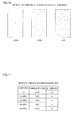
- the concentration of Cu on the surface of the non-welded-side Ni layer 12 (112) on an arbitrary straight line in either electrode arrangement position 6 of each of the test materials 1 to 8 was analyzed, and it was determined that Cu was welded (YES determination) in a case where there existed a location of measurement where the concentration of Cu was at least 73.5 %. In a case where there existed no location of measurement where the concentration of Cu was at least 73.5 %, on the other hand, it was determined that Cu was not welded (NO determination).
- test materials 1 to 7 correspond to Examples of this embodiment, while the test material 8 corresponds to comparative example.
- the thickness t1 of the non-welded-side Ni layer 12 was at least 1.3 % (test material 1) and not more than 8.4 % (test material 7) of the thickness t3 of the lead material 1.
- the non-welded-side Ni layer 12 of the lead material 1 and the electrodes 4a for resistance welding made of alumina dispersed copper can be inhibited from reacting with each other at the time of performing resistance welding by employing the lead material 1 consisting of the cladding material of Ni layer/Fe layer/Ni layer.
- the corrosion resistance evaluation test conducted as the confirmative experiment is described.
- evaluation of corrosion resistance of a plate material made of Ni and plate materials made of Ni-Fe alloys was performed. More specifically, the corrosion resistance evaluation test was conducted by employing a plate material made of Ni, a plate material made of an Ni-50Fe alloy containing 50 % of Fe, a plate material made of an Ni-58Fe alloy containing 58 % of Fe, a plate material made of an Ni-62Fe alloy containing 62 % of Fe and a plate material made of an Ni-64Fe alloy containing 64 % of Fe as test materials.
- the corrosion resistance evaluation test was conducted by spraying 5 % (50 g/L) aqueous NaCl solutions to the test materials continuously for 24 hours under a temperature condition of 35°C according to the "salt spray testing method" of JISZ2371.
- the corrosion resistance of each test material was evaluated by observing a corroded state of the test material after the test.
- the corroded state was determined with reference to the ratio of a corroded area to a constant area with reference to criteria of determination (JIS rating numbers) of corroded area ratios shown in Fig. 10 .
- the corroded area ratio reached 0.02 % in the plate material made of Ni, and it was confirmed that the plate material made of Ni was not much corroded.
- the corroded area ratios reached 0.5 % in the plate material made of the Ni-50Fe alloy, the plate material made of the Ni-58Fe alloy and the plate material made of the Ni-62Fe alloy, while the corroded area ratio was 0.25 % in the plate material made of the Ni-64Fe alloy.
- the plate materials made of the Ni-50Fe alloy, the Ni-58Fe alloy, the Ni-62Fe alloy and the Ni-64Fe alloy were more easily corroded by at least 10 times as compared with the plate material made of Ni.
- the corrosion resistance can be improved by arranging the welded-side Ni layer 11 made of Ni and the non-welded-side Ni layer 12 made of Ni on the surfaces of the lead material 1 as shown in Fig. 2 , as compared with a case where Ni-Fe alloys are arranged on surfaces of a lead material.
- the present invention is not restricted to this.
- the lead material 1 (cladding material for a lead according to the present invention) according to this embodiment may be applied to lead materials welded to anode terminals 81 and cathode terminals 82 of three secondary batteries 8 constituting a secondary battery 7 for a notebook computer by resistance welding, as shown in Fig. 12 , for example.
- the lead materials 1 are so welded as to connect the anode terminals 81 and the cathode terminals 82 of the three secondary batteries 8 with each other, and so welded as to connect the secondary battery 7 for a notebook computer and a protective circuit 3 with each other.
- the secondary batteries 8 are examples of the "battery" in the present invention
- the anode terminals 81 and the cathode terminals 82 are examples of the "terminal" in the present invention.
- the cladding material for a lead according to the present invention may be applied to a lead material welded to a terminal of a primary battery.
- the thickness t3 of the lead material 1 is at least about 0.1 mm and not more than about 0.25 mm
- the present invention is not restricted to this.
- the thickness of the lead material may be less than about 0.1 mm, or may be greater than about 0.25 mm.
- the thickness of the welded-side Ni layer (first Ni layer) must be at least about 2.1 % and not more than about 8.2 % of the thickness of the cladding material for a lead.
- the lead material 1 may be formed to consist of a three-layer cladding material only in the vicinity of a welded portion by bonding a welded-side Ni layer and a non-welded-side Ni layer only in the vicinity of the welded portion of the lead material.
- the present invention is not restricted to this.
- another Fe material such as SPCC (commercial cold-rolled steel plate) or hot-rolled steel plate may be employed as the Fe layer.
Landscapes
- Chemical & Material Sciences (AREA)
- Chemical Kinetics & Catalysis (AREA)
- Electrochemistry (AREA)
- General Chemical & Material Sciences (AREA)
- Engineering & Computer Science (AREA)
- Mechanical Engineering (AREA)
- Inorganic Chemistry (AREA)
- Materials Engineering (AREA)
- Metallurgy (AREA)
- Organic Chemistry (AREA)
- Connection Of Batteries Or Terminals (AREA)
Abstract
Description
- The present invention relates to a cladding material for a lead and a method of welding a cladding material for a lead, and more particularly, it relates to a cladding material for a lead welded to a terminal of a battery and a method of welding a cladding material for a lead.
- A lead welded to a terminal of a battery is known in general. Such a lead is disclosed in Japanese Patent Laying-Open No.
2007-35650 2007-35650 2007-35650 - Patent Document 1: Japanese Patent Laying-Open No.
2007-35650 - In the method of welding a battery container disclosed in the aforementioned Japanese Patent Laying-Open No.
2007-35650 - The present invention has been proposed in order to solve the aforementioned problem, and an object of the present invention is to provide a cladding material for a lead capable of inhibiting foreign matter from remaining on a surface and a method of welding a cladding material for a lead.
- A cladding material for a lead according to a first aspect of the present invention is a cladding material for a lead welded to a terminal of a battery, including a first Ni layer arranged on a side welded to the terminal of the battery, a second Ni layer arranged on a side opposite to the welded side and an Fe layer arranged to be held between the first Ni layer and the second Ni layer, in which the thickness of the first Ni layer is at least 2.1 % and not more than 8.2 % of the thickness of the cladding material consisting of the first Ni layer, the second Ni layer and the Fe layer.
- In the cladding material for a lead according to the first aspect of the present invention, as hereinabove described, the cladding material consisting of the first Ni layer, the second Ni layer and the Fe layer is so employed as a lead material that the second Ni layer is not formed by employing an Ni plating tank in which moisture and an impurity other than Ni are contained dissimilarly to a case of employing a material plated with Ni as the lead material, whereby the moisture and the impurity other than Ni can be inhibited from remaining on the second Ni layer arranged on the side opposite to the welded side. Thus, the moisture and the impurity other than Ni can be inhibited from gasifying due to a high temperature at the time of welding, whereby foreign matter can be inhibited from remaining on a surface of the second Ni layer due to reaction between the second Ni layer and an electrode or the like employed for the welding when welding the cladding material for a lead to the terminal of the battery. Further, the first Ni layer and the second Ni layer can be arranged on a surface of the lead material, whereby corrosion resistance of the cladding material for a lead can be improved as compared with a case of arranging an Ni-Fe alloy or the like on the surface of the lead material. In addition, the cladding material for a lead includes the Fe layer having iron lower in cost than Ni as a substrate, whereby the lead material can be prepared at a lower cost as compared with a lead material made of only Ni.
- In the aforementioned cladding material for a lead according to the first aspect, the thickness of the first Ni layer is set to at least 2.1 % and not more than 8.2 % of the thickness of the cladding material, whereby bonding strength substantially equivalent to or higher than that in the case of employing the material plated with Ni as the lead material can be obtained at a time of welding the cladding material for a lead to the terminal of the battery. The inventor has found as a result of deep studies that the bonding strength substantially equivalent to or higher than that in the case of employing the material plated with Ni as the lead material can be obtained by setting the thickness of the first Ni layer set to at least 2.1 % and not more than 8.2 % of the thickness of the cladding material.
- In the aforementioned cladding material for a lead according to the first aspect, the thickness of the first Ni layer is preferably at least 3.1 % and not more than 7.5 % of the cladding material. According to this structure, the bonding strength at the time of welding the cladding material for a lead to the terminal of the battery can be reliably ensured as compared with the case of employing the material plated with Ni as the lead material.
- In the aforementioned cladding material for a lead according to the first aspect, the thickness of the first Ni layer is preferably at least 2.1 µm and not more than 20.5 µm. According to this structure, the bonding strength substantially equivalent to or higher than that in the case of employing the material plated with Ni as the lead material can be obtained when welding the cladding material for a lead to the terminal of the battery in a case where the thickness of the cladding layer is at least 0.1 mm and not more than 0.25 mm.
- In the aforementioned cladding material for a lead according to the first aspect, the thickness of the first Ni layer and the thickness of the second Ni layer are preferably substantially equal to each other. According to this structure, the first Ni layer and the second Ni layer may not be distinguished from each other when welding the cladding material for a lead to the terminal of the battery. Thus, the cladding material for a lead can be easily welded to the terminal of the battery.
- In the aforementioned cladding material for a lead according to the first aspect, the thickness of the second Ni layer is preferably at least 1.3 % and not more than 8.4 % of the thickness of the cladding layer. According to this structure, foreign matter can be more reliably inhibited from remaining on the surface of the second Ni layer.
- In the aforementioned cladding material for a lead according to the first aspect, the first Ni layer is preferably formed to be welded to a surface of an Ni layer of the terminal of the battery including the Ni layer. According to this structure, the first Ni layer of the lead material and the Ni layer of the terminal of the battery containing the same Ni element can be welded to each other, whereby the bonding strength can be further improved and the welding can be more easily performed as compared with a case of welding layers made of other elements to each other.
- A method of welding a cladding material for a lead according to a second aspect of the present invention is a method of welding a cladding material for a lead by resistance-welding a cladding material including a first Ni layer, a second Ni layer and an Fe layer arranged to be held between the first Ni layer and the second Ni layer, in which the thickness of the first Ni layer is at least 2.1 % and not more than 8.2 % of the thickness of the cladding material consisting of the first Ni layer, the second Ni layer and the Fe layer, to a terminal of a battery, including the steps of arranging the cladding material on the terminal of the battery so that the first Ni layer is positioned on the side of the terminal of the battery and resistance-welding the first Ni layer to the terminal of the battery by feeding electricity to an electrode for resistance welding in a state of arranging the electrode on the side of the second Ni layer opposite to the side where the terminal of the battery is positioned.
- In the method of welding a cladding material for a lead according to the second aspect of the present invention, as hereinabove described, the cladding material consisting of the first Ni layer, the second Ni layer and the Fe layer is employed as a lead material resistance-welded to the terminal of the battery so that the second Ni layer is not formed by employing an Ni plating tank in which moisture and an impurity other than Ni are contained dissimilarly to a case of employing a material plated with Ni as the lead material, whereby the moisture and the impurity other than Ni can be inhibited from remaining on the second Ni layer arranged on the side opposite to the resistance-welded side. Thus, the moisture and the impurity other than Ni can be inhibited from gasifying due to a high temperature at the time of resistance welding, whereby foreign matter can be inhibited from remaining on a surface of the second Ni layer due to reaction between the second Ni layer and the electrode for resistance welding when resistance-welding the cladding material for a lead to the terminal of the battery. Further, the first Ni layer and the second Ni layer can be arranged on a surface of the lead material, whereby corrosion resistance of the cladding material for a lead can be improved as compared with a case of arranging an Ni-Fe alloy or the like on the surface of the lead material. In addition, the cladding material for a lead includes the Fe layer having iron at a lower cost than Ni as a substrate, whereby the lead material can be prepared at a lower cost as compared with a lead material made of only Ni. Further, the thickness of the first Ni layer is set to at least 2.1 % and not more than 8.2 % of the thickness of the cladding layer, whereby bonding strength substantially equivalent to or higher than that in the case of employing the material plated with Ni as the lead material can be obtained.
- In the aforementioned method of welding a cladding material for a lead according to the second aspect, the thickness of the first Ni layer is preferably at least 3.1 % and not more than 7.5 % of the thickness of the cladding material. According to this structure, the bonding strength can be reliably ensured as compared with the case of employing the material plated with Ni as the lead material.
-
- [
Fig. 1 ] A schematic diagram showing a state where lead materials according to an embodiment of the present invention are welded to an anode terminal and a cathode terminal of a secondary battery for a portable telephone. - [
Fig. 2 ] An enlarged sectional view showing a state where each lead material according to the embodiment of the present invention is welded onto a surface of the anode terminal or the cathode terminal. - [
Fig. 3 ] A perspective view showing a state at a time of welding the lead material according to the embodiment of the present invention to the anode terminal or the cathode terminal by resistance welding. - [
Fig. 4 ] A perspective view for illustrating a bonding strength evaluation test conducted for confirming effects of the present invention. - [
Fig. 5 ] A table showing results of the bonding strength evaluation test conducted for confirming effects of the present invention. - [
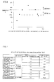
Fig. 6 ] A graph showing results of the bonding strength evaluation test conducted for confirming effects of the present invention. - [
Fig. 7 ] A table showing results of an electrode welding evaluation test conducted for confirming effects of the present invention. - [
Fig. 8 ] A graph showing a state of electrode welding in a test material 3 (Example) conducted for confirming effects of the present invention. - [
Fig. 9 ] A graph showing a state of electrode welding in a test material 8 (comparative example) conducted for confirming effects of the present invention. - [
Fig. 10 ] A diagram for illustrating a corrosion resistance evaluation test conducted for confirming effects of the present invention. - [
Fig. 11 ] A table showing results of the corrosion resistance evaluation test conducted for confirming effects of the present invention. - [
Fig. 12 ] A schematic diagram showing a state where lead materials according to the embodiment of the present invention are welded to an anode terminal and a cathode terminal of a secondary battery for a notebook computer. - An embodiment of the present invention is described on the basis of the drawings.
- First, the structure of a
lead material 1 according to the embodiment of the present invention is described with reference toFigs. 1 and2 . - As exemplary application of the
lead material 1 according to the embodiment of the present invention,lead materials 1 are welded to ananode terminal 21 and acathode terminal 22 of asecondary battery 2 for a portable telephone by resistance welding, as shown inFig. 1 . More specifically, an end portion of one of a pair oflead materials 1 is welded to theanode terminal 21 consisting of a protruding portion formed on thesecondary battery 2 for a portable telephone by resistance welding, while another end portion is connected to aprotective circuit 3. An portion of the other one of the pair oflead materials 1 is welded to thecathode terminal 22 consisting of a case portion of thesecondary battery 2 for a portable telephone by resistance welding, while another end portion is connected to theprotective circuit 3. Thelead materials 1 are examples of the "cladding material for a lead" in the present invention, thesecondary battery 2 for a portable telephone is an example of the "battery" in the present invention, and theanode terminal 21 and thecathode terminal 22 are examples of the "terminal" in the present invention. - The
protective circuit 3 is formed to control charging/discharging of thesecondary battery 2 for a portable telephone, and so formed that overcharging to thesecondary battery 2 and overdischarging from thesecondary battery 2 to a control circuit portion (not shown) are suppressed by theprotective circuit 3. - According to this embodiment, each
lead material 1 is formed by bonding a welded-side Ni layer 11 made of Ni and a non-welded-side Ni layer 12 made of Ni onto both surfaces, i.e. an upper surface and a lower surface of anFe layer 10 made of SPCD (cold-rolled steel plate for deep drawing) respectively by pressure welding, as shown inFig. 2 . In other words, thelead material 1 is formed as a cladding material consisting of three layers (Ni layer/Fe layer/Ni layer) including theFe layer 10 as a substrate. The welded-side Ni layer 11 is arranged on a side (Zi side) welded to a surface of theanode terminal 21 or thecathode terminal 22 shown inFig. 1 , while the non-welded-side Ni layer 12 is arranged on a side (Z2 side) opposite to the welded side. The welded-side Ni layer 11 is an example of the "first Ni layer" in the present invention, and the non-welded-side Ni layer 12 is an example of the "second Ni layer" in the present invention. - This embodiment is so formed that the thickness t3 of the
lead material 1 is at least about 0.1 mm and not more than about 0.25 mm while the thickness t1 of the welded-side Ni layer 11 is at least about 2.1 % and not more than about 8.2 % of the thickness t3 of thelead material 1. In other words, the embodiment is so formed that, in a case where the thickness t3 of thelead material 1 is about 0.1 mm, the thickness t1 of the welded-side Ni layer 11 is at least about 2.1 µm (about 2.1 % of the thickness t3 of the lead material 1) and not more than about 8.2 µm (about 8.2 % of the thickness t3 of the lead material 1). The thickness t1 of the welded-side Ni layer 11 is more preferably at least about 3.1 µm (about 3.1 % of the thickness t3 of the lead material 1) and not more than about 7.5 µm (about 7.5 % of the thickness t3 of the lead material 1). The thickness t1 of the welded-side Ni layer 11 is further preferably about 5.2 µm (about 5.2 % of the thickness t3 of the lead material 1). - The embodiment is so formed that, in the case where the thickness t3 of the
lead material 1 is about 0.1 mm, the thickness t2 of the non-welded-side Ni layer 12 is at least about 2.1 µm (about 2.1 % of the thickness t3 of the lead material 1) and not more than about 8.2 µm (about 8.2 % of the thickness t3 of the lead material 1). Further, the embodiment is so formed that the thickness t4 of theFe layer 10 is at least about 83.6 µm and not more than about 95.8 µm. - The embodiment is so formed that, in a case where the thickness t3 of the
lead material 1 is about 0.25 mm, the thickness t1 of the welded-side Ni layer 11 is at least about 5.3 µm (about 2.1 % of the thickness t3 of the lead material 1) and not more than about 20.5 µm (about 8.2 % of the thickness t3 of the lead material 1). The thickness t1 of the welded-side Ni layer 11 is more preferably at least about 7.8 µm (about 3.1 % of the thickness t3 of the lead material 1) and not more than about 18.8 µm (about 7.5 % of the thickness t3 of the lead material 1). The thickness t1 of the welded-side Ni layer 11 is further preferably about 13.0 µm (about 5.2 % of the thickness t3 of the lead material 1). - The embodiment is so formed that, in the case where the thickness t3 of the
lead material 1 is about 0.25 mm, the thickness t2 of the non-welded-side Ni layer 12 is at least about 5.3 µm (about 2.1 % of the thickness t3 of the lead material 1) and not more than about 20.5 µm (about 8.2 % of the thickness t3 of the lead material 1). Further, the embodiment is so formed that the thickness t4 of theFe layer 10 is at least about 159.0 µm and not more than about 189.4 µm. - This embodiment is so formed that the thickness t1 of the welded-
side Ni layer 11 and the thickness t2 of the non-welded-side Ni layer 12 are substantially equal to each other. - The
anode terminal 21 and thecathode terminal 22 includesubstrates substrates Fig. 2 . Thus, the embodiment is so formed that the welded-side Ni layer 11 of thelead material 1 is welded to the surface of theNi layer 21b of theanode terminal 21 or the surface of theNi layer 22b of thecathode terminal 22. - In a case where the
substrate 21a (22a) is made of Al, the anode terminal 21 (cathode terminal 22) is formed as a cladding material in which thesubstrate 21a (22a) and theNi layer 21b (22b) are bonded to each other. In a case where thesubstrate 21a (22a) is made of low-carbon steel, on the other hand, the anode terminal 21 (cathode terminal 22) is formed as an Ni-plated material in which thesubstrate 21a (22a) is plated with theNi layer 21b (22b). - A method of welding the
lead material 1 according to the embodiment of the present invention is now described with reference toFigs. 2 and 3 . - First, a steel plate of SPCD having a thickness of about 2 mm and Ni plates made of Ni each having a thickness of at least about 43.8 µm and not more than about 196.2 µm are prepared. In a case where the thickness of each Ni plate is about 43.8 µm, the thickness of the Ni plate is set to be about 2.1 % of the total (about 2087.6 µm) of the thickness of the steel plate of SPCD and the thicknesses of a pair of Ni plates. Similarly, in a case where the thickness of each Ni plate is about 196.2 µm, the thickness of the Ni plate is set to be about 8.2 % of the total (about 2392.4 µm) of the thickness of the steel plate of SPCD and the thicknesses of the pair of Ni plates.
- Then, the steel plate of SPCD and the pair of Ni plates are pressure-welded to each other in a state of arranging the same Ni plates on both surfaces of SPCD, so that the ratio of a thickness after rolling to a thickness before rolling is about 60 %. Thus, a cladding material of Ni layer/Fe layer/Ni layer having a thickness of at least about 0.84 mm (in the case where the thickness of each Ni plate is about 2.1 % of the total thickness) and not more than about 0.96 mm (in the case where the thickness of each Ni plate is about 8.2 % of the total thickness), in which the Ni layers are bonded onto both surfaces of the Fe layer, is prepared.
- Then, diffusion annealing is performed by holding the prepared cladding material of Ni layer/Fe layer/Ni layer having the thickness of at least about 0.84 mm and not more than about 0.96 mm in an environment of about 1000°C for about three minutes. Thereafter the
lead material 1 having the thickness t3 of at least about 0.1 mm and not more than about 0.25 mm is prepared by performing rolling. At this time, both of the thickness t1 of the welded-side Ni layer 11 and the thickness t2 of the non-welded-side Ni layer 12 are at least about 2.1 % and not more than about 8.2 % of the thickness t3 of thelead material 1. - Then, the
lead material 1 is arranged on the anode terminal 21 (cathode terminal 22) so that the welded-side Ni layer 11 of thelead material 1 is positioned on the surface of theNi layer 21b of the anode terminal 21 (surface of theNi layer 22b of the cathode terminal 22) of thesecondary battery 2, as shown inFig. 3 . This embodiment is so formed that the thickness t1 of the welded-side Ni layer 11 and the thickness t2 of the non-welded-side Ni layer 12 are substantially identical to each other, and hence either one of both surfaces of thelead material 1 may simply be arranged on the surface of theNi layer 21b (22b). In other words, the layer on the side arranged on the surface of theNi layer 21b (22b) becomes the welded-side Ni layer 11, and the layer on the side opposite to the side arranged on the surface of theNi layer 21b (22b) becomes the non-welded-side Ni layer 12. Then,columnar electrodes 4a for resistance welding, made of alumina dispersed copper, each having a diameter of about 1 mm are arranged in a pair on the surface of thelead material 1 on the side of the non-welded-side Ni layer 12. At this time, the pair ofelectrodes 4a are arranged at a distance L1 (about 4.5 mm). - The pair of
electrodes 4a are connected to apower unit 4b converting direct current to alternating current and supplying the same to the pair ofelectrodes 4a, and a DC invertertype resistance welder 4 is constituted of the pair ofelectrodes 4a and thepower unit 4b. - According to this embodiment, current of about 3.5 kA is fed to the
electrodes 4a for about 0.004 seconds (4 msec.) while pressing the pair ofelectrodes 4a against the non-welded-side Ni layer 12 of thelead material 1 with force of about 78.5 N. Thus, thelead material 1 and the anode terminal 21 (cathode terminal 22) generate heat due to electrical resistance possessed by each when current flows to thelead material 1 in the vicinity of the pair ofelectrodes 4a and the anode terminal 21 (cathode terminal 22) of thesecondary battery 2. As a result of this, the welded-side Ni layer 11 and theNi layer 21b (22b) are melted, whereby thelead material 1 and the anode terminal 21 (cathode terminal 22) are welded to each other. - Then, the
electrodes 4a are separated from the non-welded-side Ni layer 12 of thelead material 1, whereby wending of thelead material 1 to the anode terminal 21 (cathode terminal 22) is terminated. - According to this embodiment, as hereinabove described, the cladding material of three layers (Ni layer/Fe layer/Ni layer) consisting of the welded-
side Ni layer 11, the non-welded-side Ni layer 12 and theFe layer 10 is so employed as thelead material 1 that the non-welded-side Ni layer 12 is not formed by employing an Ni plating tank in which moisture and an impurity other than Ni are contained dissimilarly to a case of employing a material plated with Ni as the lead material, whereby the moisture and the impurity other than Ni can be inhibited from remaining on the non-welded-side Ni layer 12 arranged on the side opposite to the welded side. Thus, the moisture and the impurity other than Ni can be inhibited from gasifying due to a high temperature at the time of welding, whereby foreign matter can be inhibited from remaining on the non-welded-side Ni layer 12 due to reaction between the non-welded-side Ni layer 12 and the pair ofelectrodes 4a employed for the welding when welding thelead material 1 to theanode terminal 21 or thecathode terminal 22. Further, the welded-side Ni layer 11 and the non-welded-side Ni layer 12 can be arranged on the surfaces of the cladding material employed as thelead material 1, whereby corrosion resistance of thelead material 1 can be improved as compared with a case of arranging Ni-Fe alloys or the like on the surfaces of thelead material 1. In addition, thelead material 1 includes theFe layer 10 having iron lower in cost than Ni as the substrate, whereby thelead material 1 can be prepared at a lower cost as compared with a lead material made of only Ni. - According to this embodiment, as hereinabove described, the thickness t1 of the welded-
side Ni layer 11 is set to at least about 2.1 % and not more than about 8.2 % of the thickness t3 of thelead material 1, whereby bonding strength substantially equivalent to or higher than that in the case of employing the material plated with Ni as the lead material can be obtained at the time of welding thelead material 1 to theanode terminal 21 or thecathode terminal 22. - According to this embodiment, as hereinabove described, the thickness t1 of the welded-
side Ni layer 11 is set to at least about 3.1 % and not more than about 7.5 % of the thickness t3 of thelead material 1, whereby the bonding strength at the time of welding thelead material 1 to theanode terminal 21 or thecathode terminal 22 can be reliably ensured as compared with the case of employing the material plated with Ni as the lead material. - According to this embodiment, as hereinabove described, the thickness t1 of the welded-
side Ni layer 11 is set to at least 2.1 µm and not more than 20.5 µm, whereby the bonding strength substantially equivalent to or higher than that in the case of employing the material plated with Ni as the lead material can be obtained when welding thelead material 1 to theanode terminal 21 or thecathode terminal 22 in the case where the thickness t3 of thelead material 1 is at least 0.1 mm and not more than 0.25 mm. - According to this embodiment, as hereinabove described, the thickness t1 of the welded-
side Ni layer 11 and the thickness t2 of the non-welded-side Ni layer 12 are substantially equalized to each other, whereby the welded-side Ni layer 11 and the non-welded-side Ni layer 12 may not be distinguished from each other when welding thelead material 1 to theanode terminal 21 or thecathode terminal 22. Thus, thelead material 11 can be easily welded to theanode terminal 21 or thecathode terminal 22. - Further, the thickness t2 of the non-welded-
side Ni layer 12 is set to at least about 2.1 % and not more than about 8.2 % of the thickness t3 of thelead material 1, whereby foreign matter can be more reliably inhibited from remaining on the non-welded-side Ni layer 12. - According to this embodiment, as hereinabove described, the thickness t1 of the welded-
side Ni layer 11 is so welded to the surface of theNi layer 21b of the anode terminal 21 (surface of theNi layer 22b of the cathode terminal 22) that the welded-side Ni layer 11 and theNi layer 21b (22b) containing the same Ni element can be welded to each other, whereby the bonding strength can be more improved and the welding can be easily performed as compared with a case of welding layers made of different elements to each other. - While the example of substantially equalizing the thickness t1 of the welded-
side Ni layer 11 and the thickness t2 of the non-welded-side Ni layer 12 to each other has been shown in the aforementioned embodiment, the thickness t1 of the welded-side Ni layer 11 and the thickness t2 of the non-welded-side Ni layer 12 may be rendered different from each other, as a modification of the aforementioned embodiment. In this case, the thickness t1 of the welded-side Ni layer 11 is at least about 2.1 % and not more than about 8.2 % of the thickness t3 of thelead material 1, while the thickness t2 of the non-welded-side Ni layer 12 may be less than about 2.1 % of the thickness t3 of thelead material 1, or may be greater than about 8.2 % of the thickness t3 of thelead material 1. The thickness t2 of the non-welded-side Ni layer 12 is more preferably at least about 1.3 % and not more than about 8.4 % of the thickness t3 of thelead material 1, in order to more reliably inhibit foreign matter from remaining on the surface of the non-welded-side Ni layer 12. - Confirmative experiments related to a bonding strength evaluation test, an electrode welding evaluation test and a corrosion resistance evaluation test conducted for confirming effects according to this embodiment are now described with reference to
Figs. 2 to 11 . - In the bonding strength evaluation test and the electrode welding evaluation test described below,
lead materials 1, having thicknesses t3 (seeFig. 2 ) of 0.1 mm, so formed that thicknesses t1 of welded-side Ni layers 11 (thicknesses t2 of non-welded-side Ni layers 12: seeFig. 2 ) were different from each other were prepared in plural astest materials 1 to 7 corresponding to thelead material 1 according to this embodiment, by employing the aforementioned method of welding thelead material 1 according to this embodiment. At this time, eachlead material 1 was so prepared that the thickness t1 of the welded-side Ni layer 11 and the thickness t2 of the non-welded-side Ni layer 12 were identical to each other. - More specifically, the thickness t1 of the welded-side Ni layer 11 (thickness t2 of the non-welded-side Ni layer 12) was set to 1.3 µm (1.3 % of the thickness t3 (0.1 mm) of the lead material 1) in the
lead material 1 of thetest material 1, as shown inFigs. 5 and7 . In thelead material 1 of thetest material 2, the thickness t1 of the welded-side Ni layer 11 (thickness t2 of the non-welded-side Ni layer 12) was set to 2.1 µm (2.1 % of the thickness t3 of the lead material 1). - In the
lead material 1 of thetest material 3, the thickness t1 of the welded-side Ni layer 11 (thickness t2 of the non-welded-side Ni layer 12) was set to 3.1 µm (3.1 % of the thickness t3 of the lead material 1). In thelead material 1 of thetest material 4, the thickness t1 of the welded-side Ni layer 11 (thickness t2 of the non-welded-side Ni layer 12) was set to 5.2 µm (5.2 % of the thickness t3 of the lead material 1). - In the
lead material 1 of thetest material 5, the thickness t1 of the welded-side Ni layer 11 (thickness t2 of the non-welded-side Ni layer 12) was set to 7.5 µm (7.5 % of the thickness t3 of the lead material 1). In thelead material 1 of thetest material 6, the thickness t1 of the welded-side Ni layer 11 (thickness t2 of the non-welded-side Ni layer 12) was set to 8.2 µm (8.2 % of the thickness t3 of the lead material 1). - In the
lead material 1 of thetest material 7, the thickness t1 of the welded-side Ni layer 11 (thickness t2 of the non-welded-side Ni layer 12) was set to 8.4 µm (8.4 % of the thickness t3 of the lead material 1). - On the other hand, a lead material 101 (see
Fig. 4 ) in which a welded-side Ni layer 111 and a non-welded-side Ni layer 112 (seeFig. 4 ) formed on both surfaces of anFe layer 10 are plated layers of Ni was prepared as atest material 8 to be compared with thelead material 1 consisting of the cladding material of Ni layer/Fe layer/Ni layer according to this embodiment. In other words, thelead material 101 consists of an Ni-plated material. At this time, the thickness of thelead material 101 was set to 0.1 mm, while the thicknesses of the welded-side Ni layer 111 and the non-welded-side Ni layer 112 were set to 2.5 µm. - Then, current of 3.5 kA was fed to
electrodes 4a for 0.004 seconds while pressing theelectrodes 4a (seeFig. 3 ) against the non-welded-side Ni layer 12 (112) of each lead material 1 (101) with force of 78.5 N so that the welded-side Ni layer 11 (111) of the lead material 1 (101) was positioned on a surface of a welding base material 5 (seeFig. 4 ) made of low-carbon steel. Thus, each of the lead materials 1 (101) of theprepared test materials 1 to 8 was welded to thewelding base material 5 by resistance welding. - In these evaluation tests (the bonding strength evaluation test and the electrode welding evaluation test), the evaluation tests were conducted by employing the
welding base material 5 having no Ni layers 21b and 22b (seeFig. 2 ) for improving bonding strength, in place of theanode terminal 21 and thecathode terminal 22 in the aforementioned embodiment. This is in order to obtain conditions for obtaining bonding strength of at least reference strength described later in a state of not providing the Ni layers 21b and 22b improving the bonding strength in these evaluation tests. - The bonding strength evaluation test is now described. In this bonding strength evaluation test, the lead material 1 (101) of each of the
test materials 1 to 8 and thewelding base material 5 resistance-welded to each other were pulled in directions opposite to each other at a speed of 10 mm/min., to obtain tensile strength at a time when welded portions were broken as bonding strength. - In the bonding strength evaluation test, the
test materials 2 to 6 correspond to Examples of this embodiment, while thetest materials - In the bonding strength evaluation test, bonding strength was determined while regarding the bonding strength of the test material 8 (comparative example) employed in general as reference strength. In other words, in a case where a certain test material had bonding strength exceeding the bonding strength (126.5N shown in
Fig. 5 ) of thetest material 8, the test material was determined as having sufficient bonding strength (single circle determination), while in a case where another certain test material had bonding strength less than the bonding strength of thetest material 8, the test material was determined as not having sufficient bonding strength (cross determination). In a case where still another certain test material had bonding strength of at least 176.5N, greater than the bonding strength (126.5N) of thetest material 8 by 50N, further, the test material was determined as having more preferable bonding strength (double circle determination). - As results of the bonding strength evaluation test shown in
Figs. 5 and6 , the bonding strength reached 69.6N in the test material 1 (comparative example), while the bonding strength reached 121.6N in the test material 7 (comparative example), and became bonding strength less than the bonding strength (126.5N) of thetest material 8. In thetest materials 2 to 6 (Examples), on the other hand, the bonding strength reached at least 128.5N (test material 2) and not more than 221.6N (test material 6), and became bonding strength exceeding the bonding strength (126.5N) of thetest material 8. Thus, it could be confirmed that bonding strength substantially equivalent to or higher than that of thetest material 8 can be obtained in the case where the thickness t1 of the welded-side Ni layer 11 is at least 2.1 % (test material 2) and not more than 8.2 % (test material 6) of the thickness t3 of thelead material 1. - In the
test materials 3 to 5 (Examples), the bonding strength reached at least 176.5N (test material 3) and not more than 221.6N (test material 4), and became bonding strength of at least 176.5N. Thus, it could be confirmed that bonding strength greater than that of the test material 8 (comparative example) by at least 50N is obtained in the case where the thickness t1 of the welded-side Ni layer 11 is at least 3.1 % (test material 3) and not more than 7.5 % (test material 5) of the thickness t3 of thelead material 1. In the test material 4 (Example), the bonding strength reached the maximum (221.6N). Thus, it could be confirmed that the bonding strength is maximized in the case where the thickness t1 of the welded-side Ni layer 11 is 5.2 % of the thickness t3 of thelead material 1. - The bonding strength reached the maximum in the test material 4 (thickness t1 of the welded-
side Ni layer 11 was 5.2 µm) conceivably because the thickness t1 of the welded-side Ni layer 11 contributing to welding was small and the quantity of Ni contributing to the welding was small in the case where the thickness t1 of the welded-side Ni layer 11 was smaller than 5.2 µm (test materials 1 to 3) and hence the bonding strength became small as compared with thetest material 4. Further, Ni of the welded-side Ni layer 11 has smaller electric resistance and larger thermal conductivity as compared with theFe layer 10. In the case where the thickness t1 of the welded-side Ni layer 11 is greater than 5.2 µm (test materials 5 to 7), therefore, it is conceivable that heat generation resulting from flowing current is small and generated heat is easily conducted to the whole of the welded-side Ni layer 11 at the time of resistance welding. In thetest materials 5 to 7, therefore, it is conceivable that the quantity of heat employed for resistance welding became smaller as compared with thetest material 4 and hence the bonding strength resulting from welding became small. - The electrode welding evaluation test is now described. In this electrode welding evaluation test, the surface of the non-welded Ni layer 12 (112) on
electrode arrangement positions 6 of each of thetest materials 1 to 8 shown inFig. 4 where theelectrodes 4a (seeFig. 3 ) had been arranged was analyzed with an electron probe microanalyzer (EPMA) after the welding by resistance welding, and presence or absence of welding of Cu contained in theelectrodes 4a was confirmed. More specifically, the concentration of Cu on the surface of the non-welded-side Ni layer 12 (112) on an arbitrary straight line in eitherelectrode arrangement position 6 of each of thetest materials 1 to 8 was analyzed, and it was determined that Cu was welded (YES determination) in a case where there existed a location of measurement where the concentration of Cu was at least 73.5 %. In a case where there existed no location of measurement where the concentration of Cu was at least 73.5 %, on the other hand, it was determined that Cu was not welded (NO determination). - In the electrode welding evaluation test, the
test materials 1 to 7 correspond to Examples of this embodiment, while thetest material 8 corresponds to comparative example. - As results of the electrode welding evaluation test shown in
Fig. 7 , no welding of Cu was confirmed in any of thetest materials 1 to 7 (Examples) of thelead materials 1 consisting of cladding materials of Ni layers/Fe layers/Ni layers. On the surface of the non-welded-side Ni layer 12 on theelectrode arrangement positions 6 of the test material 3 (thickness t1 of the non-welded-side Ni layer 12 is 3.1 µm) shown inFig. 8 , for example, only welding of Cu in a concentration of about 10 % could be confirmed at a maximum, and there existed no location of measurement where the concentration of Cu was at least 73.5 %. Thus, it could be confirmed that there was no welding of theelectrodes 4a in the case where the thickness t1 of the non-welded-side Ni layer 12 was at least 1.3 % (test material 1) and not more than 8.4 % (test material 7) of the thickness t3 of thelead material 1. - In the test material 8 (comparative example) of the
lead material 101 in which the non-welded-side Ni layer 112 consisted of the plated layer of Ni, on the other hand, welding of Cu in a concentration of about 90 % was confirmed on locations of measurement from 1.1 mm to 1.5 mm on the surface of the non-welded-side Ni layer 112 on theelectrode arrangement positions 6, as shown inFig. 9 . Thus, there existed locations of measurement where the concentrations of Cu were at least 73.5 %, and hence it could be confirmed that welding of theelectrodes 4a took place in thelead material 101 whose non-welded-side Ni layer 112 consisted of the plated layer of Ni. Thus, it could be confirmed that the non-welded-side Ni layer 12 of thelead material 1 and theelectrodes 4a for resistance welding made of alumina dispersed copper can be inhibited from reacting with each other at the time of performing resistance welding by employing thelead material 1 consisting of the cladding material of Ni layer/Fe layer/Ni layer. - Finally, the corrosion resistance evaluation test conducted as the confirmative experiment is described. In this confirmative experiment, evaluation of corrosion resistance of a plate material made of Ni and plate materials made of Ni-Fe alloys was performed. More specifically, the corrosion resistance evaluation test was conducted by employing a plate material made of Ni, a plate material made of an Ni-50Fe alloy containing 50 % of Fe, a plate material made of an Ni-58Fe alloy containing 58 % of Fe, a plate material made of an Ni-62Fe alloy containing 62 % of Fe and a plate material made of an Ni-64Fe alloy containing 64 % of Fe as test materials. The corrosion resistance evaluation test was conducted by spraying 5 % (50 g/L) aqueous NaCl solutions to the test materials continuously for 24 hours under a temperature condition of 35°C according to the "salt spray testing method" of JISZ2371. The corrosion resistance of each test material was evaluated by observing a corroded state of the test material after the test. The corroded state was determined with reference to the ratio of a corroded area to a constant area with reference to criteria of determination (JIS rating numbers) of corroded area ratios shown in
Fig. 10 . - As results of the corrosion resistance evaluation test shown in
Fig. 11 , the corroded area ratio reached 0.02 % in the plate material made of Ni, and it was confirmed that the plate material made of Ni was not much corroded. On the other hand, the corroded area ratios reached 0.5 % in the plate material made of the Ni-50Fe alloy, the plate material made of the Ni-58Fe alloy and the plate material made of the Ni-62Fe alloy, while the corroded area ratio was 0.25 % in the plate material made of the Ni-64Fe alloy. As a result of this, it could be confirmed that the plate materials made of the Ni-50Fe alloy, the Ni-58Fe alloy, the Ni-62Fe alloy and the Ni-64Fe alloy were more easily corroded by at least 10 times as compared with the plate material made of Ni. Thus, it could be confirmed that the corrosion resistance can be improved by arranging the welded-side Ni layer 11 made of Ni and the non-welded-side Ni layer 12 made of Ni on the surfaces of thelead material 1 as shown inFig. 2 , as compared with a case where Ni-Fe alloys are arranged on surfaces of a lead material. - The embodiment and Examples disclosed this time must be considered as illustrative in all points and not restrictive. The range of the present invention is shown not by the above description of the embodiment and Examples but by the scope of claims for patent, and all modifications within the meaning and range equivalent to the scope of claims for patent are further included.
- For example, while the example of applying the
lead material 1 to the lead materials welded to theanode terminal 21 and thecathode terminal 22 of thesecondary battery 2 for a portable telephone by resistance welding has been shown in the aforementioned embodiment, the present invention is not restricted to this. The lead material 1 (cladding material for a lead according to the present invention) according to this embodiment may be applied to lead materials welded toanode terminals 81 andcathode terminals 82 of threesecondary batteries 8 constituting asecondary battery 7 for a notebook computer by resistance welding, as shown inFig. 12 , for example. In this application example, thelead materials 1 are so welded as to connect theanode terminals 81 and thecathode terminals 82 of the threesecondary batteries 8 with each other, and so welded as to connect thesecondary battery 7 for a notebook computer and aprotective circuit 3 with each other. Thesecondary batteries 8 are examples of the "battery" in the present invention, and theanode terminals 81 and thecathode terminals 82 are examples of the "terminal" in the present invention. As an application example other than the aforementioned application example, the cladding material for a lead according to the present invention may be applied to a lead material welded to a terminal of a primary battery. - While the example in which the thickness t3 of the
lead material 1 is at least about 0.1 mm and not more than about 0.25 mm has been shown in the aforementioned embodiment, the present invention is not restricted to this. According to the present invention, the thickness of the lead material may be less than about 0.1 mm, or may be greater than about 0.25 mm. Also in this case, the thickness of the welded-side Ni layer (first Ni layer) must be at least about 2.1 % and not more than about 8.2 % of the thickness of the cladding material for a lead. - While the example of forming the
lead material 1 by bonding the welded-side Ni layer 11 and the non-welded-side Ni layer 12 onto both surfaces of theFe layer 10 respectively has been shown in the aforementioned embodiment, the present invention is not restricted to this. According to the present invention, the lead material may be formed to consist of a three-layer cladding material only in the vicinity of a welded portion by bonding a welded-side Ni layer and a non-welded-side Ni layer only in the vicinity of the welded portion of the lead material. - While the example of employing the SPCD (cold-rolled steel plate for deep drawing) as the
Fe layer 10 of thelead material 1 has been shown in the aforementioned embodiment, the present invention is not restricted to this. According to the present invention, another Fe material such as SPCC (commercial cold-rolled steel plate) or hot-rolled steel plate may be employed as the Fe layer.
Claims (8)
- A cladding material (1) for a lead welded to a terminal (21, 22) of a battery (2), comprising:a first Ni layer (11) arranged on a side welded to the terminal of said battery;a second Ni layer (12) arranged on a side opposite to said welded side; andan Fe layer (10) arranged to be held between said first Ni layer and said second Ni layer, whereinthe thickness of said first Ni layer is at least 2.1 % and not more than 8.2 % of the thickness of said cladding material consisting of said first Ni layer, said second Ni layer and said Fe layer.
- The cladding material for a lead according to claim 1, wherein
the thickness of said first Ni layer is at least 3.1 % and not more than 7.5 % of the thickness of said cladding material. - The cladding material for a lead according to claim 1 or 2, wherein
the thickness of said first Ni layer is at least 2.1 µm and not more than 20.5 µm. - The cladding material for a lead according to any of claims 1 to 3, wherein
the thickness of said first Ni layer and the thickness of said second Ni layer are substantially equal to each other. - The cladding material for a lead according to any of claims 1 to 4, wherein
the thickness of said second Ni layer is at least 1.3 % and not more than 8.4 % of the thickness of said cladding layer. - The cladding material for a lead according to any of claims 1 to 5, wherein
said first Ni layer is formed to be welded to a surface of an Ni layer (21b, 22b) of the terminal of said battery including said Ni layer. - A method of welding a cladding material for a lead by resistance-welding a cladding material (1) including a first Ni layer (11), a second Ni layer (12) and an Fe layer (10) arranged to be held between said first Ni layer and said second Ni layer, wherein the thickness of said first Ni layer is at least 2.1 % and not more than 8.2 % of the thickness of said cladding material consisting of said first Ni layer, said second Ni layer and said Fe layer, to a terminal (21, 22) of a battery (2), comprising the steps of:
arranging said cladding material on the terminal of said battery so that said first Ni layer is positioned on the side of the terminal of said battery; and
resistance-welding said first Ni layer to the terminal of said battery by feeding electricity to an electrode (4a) for resistance welding in a state of arranging the electrode on the side of said second Ni layer opposite to the side where the terminal of said battery is positioned. - The method of welding a cladding material for a lead according to claim 7, wherein
the thickness of said first Ni layer is at least 3.1 % and not more than 7.5 % of the thickness of said cladding material.
Applications Claiming Priority (1)
| Application Number | Priority Date | Filing Date | Title |
|---|---|---|---|
| PCT/JP2010/052182 WO2011099160A1 (en) | 2010-02-15 | 2010-02-15 | Cladding material for leads and method of welding cladding material for leads |
Publications (3)
| Publication Number | Publication Date |
|---|---|
| EP2538472A1 true EP2538472A1 (en) | 2012-12-26 |
| EP2538472A4 EP2538472A4 (en) | 2013-07-03 |
| EP2538472B1 EP2538472B1 (en) | 2017-03-29 |
Family
ID=44367460
Family Applications (1)
| Application Number | Title | Priority Date | Filing Date |
|---|---|---|---|
| EP10845754.0A Active EP2538472B1 (en) | 2010-02-15 | 2010-02-15 | Cladding material for leads and method of welding cladding material for leads |
Country Status (6)
| Country | Link |
|---|---|
| US (1) | US20120292294A1 (en) |
| EP (1) | EP2538472B1 (en) |
| JP (1) | JP4944279B2 (en) |
| KR (1) | KR101228722B1 (en) |
| CN (1) | CN102652373B (en) |
| WO (1) | WO2011099160A1 (en) |
Families Citing this family (6)
| Publication number | Priority date | Publication date | Assignee | Title |
|---|---|---|---|---|
| DE102012008816A1 (en) * | 2012-05-07 | 2013-11-07 | Bernhard STUTH | Process for producing a metallic layer composite, in particular band-shaped layer composite |
| JP6421595B2 (en) * | 2014-12-26 | 2018-11-14 | 日立金属株式会社 | Hermetic sealing lid material, method for manufacturing hermetic sealing lid material, and electronic component storage package |
| CN111889858A (en) * | 2020-07-15 | 2020-11-06 | 芜湖天弋能源科技有限公司 | Resistance welding structure and welding method of lithium ion battery |
| US12611725B2 (en) * | 2021-03-09 | 2026-04-28 | Osaka University | Dissimilar material solid-phase bonding method and dissimilar material solid-phase bonded structure |
| CN118251287B (en) * | 2021-11-12 | 2025-01-10 | 日本制铁株式会社 | Welding components |
| US20250196790A1 (en) * | 2023-12-19 | 2025-06-19 | GM Global Technology Operations LLC | Methods of Joining Multilayer Copper-Graphene Coated Current Collectors to Battery Cans and Between Windings in Electric Motor Stators |
Family Cites Families (15)
| Publication number | Priority date | Publication date | Assignee | Title |
|---|---|---|---|---|
| US3775182A (en) * | 1972-02-25 | 1973-11-27 | Du Pont | Tubular electrochemical cell with coiled electrodes and compressed central spindle |
| JPS61118962A (en) | 1984-11-14 | 1986-06-06 | Shin Kobe Electric Mach Co Ltd | Lead plate for connecting nickel-cadmium storage battery |
| US4826736A (en) * | 1985-06-14 | 1989-05-02 | Sumitomo Special Metals Co., Ltd. | Clad sheets |
| US4737418A (en) * | 1986-12-22 | 1988-04-12 | Advanced Materials Technology Corp. | Nickel clad corrosion resistant lid for semiconductor package |
| US5553770A (en) * | 1994-03-07 | 1996-09-10 | Texas Instruments Incorporated | Heat exchanger assemblies-material for use therin, and a method of making the material |
| JPH10241697A (en) * | 1997-02-21 | 1998-09-11 | Matsushita Electric Ind Co Ltd | Electrode for alkaline storage battery and method for producing the same |
| TW502467B (en) * | 1998-03-18 | 2002-09-11 | Toshiba Battery | Battery, lead member for battery connection, and battery pack using the same |
| DE69806722T2 (en) * | 1998-03-27 | 2003-03-13 | Katayama Special Industries, Ltd. | Sheet for battery case and method of making the sheet |
| JP2000164194A (en) | 1998-11-30 | 2000-06-16 | Toshiba Battery Co Ltd | Battery lead material and battery pack using the same |
| KR100890715B1 (en) * | 2000-11-01 | 2009-03-27 | 소니 가부시끼 가이샤 | Battery, Method for Manufacturing Battery, Method for Manufacturing Weld and Pedestal |
| JP2003019569A (en) | 2001-07-04 | 2003-01-21 | At Battery:Kk | Resistance welding method, battery pack manufactured using the same |
| KR100493887B1 (en) * | 2002-08-09 | 2005-06-08 | 한국과학기술연구원 | Clad sheets for corrosion resistance and fabricating method thereof |
| JP4492342B2 (en) * | 2004-12-24 | 2010-06-30 | 日立電線株式会社 | Brazing clad material, brazing method using the same, and brazed product |
| US8088508B2 (en) * | 2005-01-31 | 2012-01-03 | Panasonic Corporation | Thermal battery |
| JP2007035650A (en) | 2006-10-02 | 2007-02-08 | Toshiba Battery Co Ltd | Battery container welding method |
-
2010
- 2010-02-15 WO PCT/JP2010/052182 patent/WO2011099160A1/en not_active Ceased
- 2010-02-15 EP EP10845754.0A patent/EP2538472B1/en active Active
- 2010-02-15 CN CN201080056076.6A patent/CN102652373B/en active Active
- 2010-02-15 KR KR1020127017626A patent/KR101228722B1/en active Active
- 2010-02-15 JP JP2011549371A patent/JP4944279B2/en active Active
-
2012
- 2012-08-02 US US13/564,942 patent/US20120292294A1/en not_active Abandoned
Also Published As
| Publication number | Publication date |
|---|---|
| CN102652373B (en) | 2014-08-20 |
| CN102652373A (en) | 2012-08-29 |
| JPWO2011099160A1 (en) | 2013-06-13 |
| JP4944279B2 (en) | 2012-05-30 |
| US20120292294A1 (en) | 2012-11-22 |
| KR101228722B1 (en) | 2013-02-01 |
| EP2538472B1 (en) | 2017-03-29 |
| EP2538472A4 (en) | 2013-07-03 |
| WO2011099160A1 (en) | 2011-08-18 |
| KR20120084336A (en) | 2012-07-27 |
Similar Documents
| Publication | Publication Date | Title |
|---|---|---|
| US9979004B2 (en) | Clad material | |
| US11355871B2 (en) | Joint of copper terminal and aluminium conductor and ultrasonic welding method hereof | |
| EP2538472B1 (en) | Cladding material for leads and method of welding cladding material for leads | |
| US10026947B2 (en) | Battery terminal and method for manufacturing battery | |
| KR101240890B1 (en) | Titanium fuel cell separator | |
| JP5202772B1 (en) | Battery negative terminal | |
| US20130171494A1 (en) | Contact element for diverters of electrochemical cells | |
| JP2016207258A (en) | Clad material for battery negative electrode lead material and method of manufacturing clad material for battery negative electrode lead material | |
| US20110274964A1 (en) | Battery Tabs and Method of Making the Same | |
| EP3152049B1 (en) | Low nickel, multiple layer laminate composite | |
| JP2021157897A (en) | Terminal seal structure | |
| JP6610098B2 (en) | Ni-plated steel foil, battery conductive member, and method for producing Ni-plated steel foil | |
| HK1177555A (en) | Cladding material for leads and method of welding cladding material for leads | |
| US20140038013A1 (en) | Method for manufacturing a connecting contact for an electrode of an electrochemical store, method for manufacturing an electrochemical store, and electrochemical store | |
| US20140134473A1 (en) | Electrical interconnect and method of assembling a rechargeable battery | |
| HK1177555B (en) | Cladding material for leads and method of welding cladding material for leads | |
| JP2006139987A (en) | Plate-like wiring material for battery pack and battery pack | |
| KR101579489B1 (en) | Surface-treated copper foil, method for manufacturing same, electrode for lithium ion secondary battery, and lithium ion secondary battery | |
| WO2007071425A1 (en) | Plate or strip for producing connectors, connector and use thereof, and process for manufacturing such a strip | |
| JP5669352B2 (en) | Dissimilar material joint with excellent corrosion resistance against contact corrosion of dissimilar metals | |
| JP2009233723A (en) | Method for manufacturing joint material, and joint material | |
| CA3065848C (en) | Joint of copper terminal and aluminium conductor and ultrasonic welding method thereof | |
| JP2007035650A (en) | Battery container welding method | |
| JP2008210730A (en) | Battery pack and welding method thereof | |
| US20140134471A1 (en) | Electrical interconnect and method of assembling a rechargeable battery |
Legal Events
| Date | Code | Title | Description |
|---|---|---|---|
| PUAI | Public reference made under article 153(3) epc to a published international application that has entered the european phase |
Free format text: ORIGINAL CODE: 0009012 |
|
| 17P | Request for examination filed |
Effective date: 20120724 |
|
| AK | Designated contracting states |
Kind code of ref document: A1 Designated state(s): AT BE BG CH CY CZ DE DK EE ES FI FR GB GR HR HU IE IS IT LI LT LU LV MC MK MT NL NO PL PT RO SE SI SK SM TR |
|
| DAX | Request for extension of the european patent (deleted) | ||
| A4 | Supplementary search report drawn up and despatched |
Effective date: 20130531 |
|
| RIC1 | Information provided on ipc code assigned before grant |
Ipc: B23K 35/02 20060101ALI20130524BHEP Ipc: H01M 2/20 20060101ALI20130524BHEP Ipc: H01M 10/46 20060101ALI20130524BHEP Ipc: B32B 15/01 20060101ALI20130524BHEP Ipc: H01M 2/32 20060101ALI20130524BHEP Ipc: H01M 2/22 20060101AFI20130524BHEP |
|
| REG | Reference to a national code |
Ref country code: HK Ref legal event code: DE Ref document number: 1177555 Country of ref document: HK |
|
| 17Q | First examination report despatched |
Effective date: 20140915 |
|
| RIC1 | Information provided on ipc code assigned before grant |
Ipc: H01M 2/32 20060101ALI20150616BHEP Ipc: B32B 15/01 20060101ALI20150616BHEP Ipc: H01M 2/20 20060101ALI20150616BHEP Ipc: H01M 2/22 20060101AFI20150616BHEP Ipc: H01M 10/46 20060101ALN20150616BHEP Ipc: C22C 38/08 20060101ALI20150616BHEP Ipc: B23K 11/20 20060101ALI20150616BHEP Ipc: B23K 35/02 20060101ALI20150616BHEP Ipc: B23K 35/30 20060101ALI20150616BHEP |
|
| GRAP | Despatch of communication of intention to grant a patent |
Free format text: ORIGINAL CODE: EPIDOSNIGR1 |
|
| RIC1 | Information provided on ipc code assigned before grant |
Ipc: H01M 10/46 20060101ALN20160809BHEP Ipc: B23K 35/30 20060101ALI20160809BHEP Ipc: B32B 15/01 20060101ALI20160809BHEP Ipc: B23K 11/20 20060101ALI20160809BHEP Ipc: C22C 38/08 20060101ALI20160809BHEP Ipc: H01M 2/20 20060101ALI20160809BHEP Ipc: H01M 2/22 20060101AFI20160809BHEP Ipc: H01M 2/32 20060101ALI20160809BHEP |
|
| INTG | Intention to grant announced |
Effective date: 20160829 |
|
| RIN1 | Information on inventor provided before grant (corrected) |
Inventor name: ODA, YOSHIMITSU Inventor name: ISHIO, MASAAKI |
|
| GRAS | Grant fee paid |
Free format text: ORIGINAL CODE: EPIDOSNIGR3 |
|
| GRAJ | Information related to disapproval of communication of intention to grant by the applicant or resumption of examination proceedings by the epo deleted |
Free format text: ORIGINAL CODE: EPIDOSDIGR1 |
|
| GRAL | Information related to payment of fee for publishing/printing deleted |
Free format text: ORIGINAL CODE: EPIDOSDIGR3 |
|
| REG | Reference to a national code |
Ref country code: DE Ref legal event code: R079 Ref document number: 602010041197 Country of ref document: DE Free format text: PREVIOUS MAIN CLASS: H01M0002300000 Ipc: H01M0002220000 |
|
| GRAR | Information related to intention to grant a patent recorded |
Free format text: ORIGINAL CODE: EPIDOSNIGR71 |
|
| RIN1 | Information on inventor provided before grant (corrected) |
Inventor name: ISHIO, MASAAKI Inventor name: ODA, YOSHIMITSU |
|
| INTC | Intention to grant announced (deleted) | ||
| RAP1 | Party data changed (applicant data changed or rights of an application transferred) |
Owner name: HITACHI METALS, LTD. |
|
| RIC1 | Information provided on ipc code assigned before grant |
Ipc: H01M 2/20 20060101ALI20170117BHEP Ipc: H01M 10/46 20060101ALN20170117BHEP Ipc: H01M 2/32 20060101ALI20170117BHEP Ipc: C22C 38/08 20060101ALI20170117BHEP Ipc: B23K 11/20 20060101ALI20170117BHEP Ipc: B23K 35/30 20060101ALI20170117BHEP Ipc: B32B 15/01 20060101ALI20170117BHEP Ipc: H01M 2/22 20060101AFI20170117BHEP |
|
| GRAA | (expected) grant |
Free format text: ORIGINAL CODE: 0009210 |
|
| INTG | Intention to grant announced |
Effective date: 20170127 |
|
| AK | Designated contracting states |
Kind code of ref document: B1 Designated state(s): AT BE BG CH CY CZ DE DK EE ES FI FR GB GR HR HU IE IS IT LI LT LU LV MC MK MT NL NO PL PT RO SE SI SK SM TR |
|
| REG | Reference to a national code |
Ref country code: GB Ref legal event code: FG4D |
|
| REG | Reference to a national code |
Ref country code: CH Ref legal event code: EP |
|
| REG | Reference to a national code |
Ref country code: AT Ref legal event code: REF Ref document number: 880515 Country of ref document: AT Kind code of ref document: T Effective date: 20170415 |
|
| REG | Reference to a national code |
Ref country code: IE Ref legal event code: FG4D |
|
| REG | Reference to a national code |
Ref country code: DE Ref legal event code: R096 Ref document number: 602010041197 Country of ref document: DE |
|
| PG25 | Lapsed in a contracting state [announced via postgrant information from national office to epo] |
Ref country code: HR Free format text: LAPSE BECAUSE OF FAILURE TO SUBMIT A TRANSLATION OF THE DESCRIPTION OR TO PAY THE FEE WITHIN THE PRESCRIBED TIME-LIMIT Effective date: 20170329 Ref country code: FI Free format text: LAPSE BECAUSE OF FAILURE TO SUBMIT A TRANSLATION OF THE DESCRIPTION OR TO PAY THE FEE WITHIN THE PRESCRIBED TIME-LIMIT Effective date: 20170329 Ref country code: NO Free format text: LAPSE BECAUSE OF FAILURE TO SUBMIT A TRANSLATION OF THE DESCRIPTION OR TO PAY THE FEE WITHIN THE PRESCRIBED TIME-LIMIT Effective date: 20170629 Ref country code: LT Free format text: LAPSE BECAUSE OF FAILURE TO SUBMIT A TRANSLATION OF THE DESCRIPTION OR TO PAY THE FEE WITHIN THE PRESCRIBED TIME-LIMIT Effective date: 20170329 Ref country code: GR Free format text: LAPSE BECAUSE OF FAILURE TO SUBMIT A TRANSLATION OF THE DESCRIPTION OR TO PAY THE FEE WITHIN THE PRESCRIBED TIME-LIMIT Effective date: 20170630 |
|
| REG | Reference to a national code |
Ref country code: NL Ref legal event code: MP Effective date: 20170329 |
|
| REG | Reference to a national code |
Ref country code: AT Ref legal event code: MK05 Ref document number: 880515 Country of ref document: AT Kind code of ref document: T Effective date: 20170329 |
|
| PG25 | Lapsed in a contracting state [announced via postgrant information from national office to epo] |
Ref country code: BG Free format text: LAPSE BECAUSE OF FAILURE TO SUBMIT A TRANSLATION OF THE DESCRIPTION OR TO PAY THE FEE WITHIN THE PRESCRIBED TIME-LIMIT Effective date: 20170629 Ref country code: SE Free format text: LAPSE BECAUSE OF FAILURE TO SUBMIT A TRANSLATION OF THE DESCRIPTION OR TO PAY THE FEE WITHIN THE PRESCRIBED TIME-LIMIT Effective date: 20170329 Ref country code: LV Free format text: LAPSE BECAUSE OF FAILURE TO SUBMIT A TRANSLATION OF THE DESCRIPTION OR TO PAY THE FEE WITHIN THE PRESCRIBED TIME-LIMIT Effective date: 20170329 |
|
| PG25 | Lapsed in a contracting state [announced via postgrant information from national office to epo] |
Ref country code: NL Free format text: LAPSE BECAUSE OF FAILURE TO SUBMIT A TRANSLATION OF THE DESCRIPTION OR TO PAY THE FEE WITHIN THE PRESCRIBED TIME-LIMIT Effective date: 20170329 |
|
| PG25 | Lapsed in a contracting state [announced via postgrant information from national office to epo] |
Ref country code: EE Free format text: LAPSE BECAUSE OF FAILURE TO SUBMIT A TRANSLATION OF THE DESCRIPTION OR TO PAY THE FEE WITHIN THE PRESCRIBED TIME-LIMIT Effective date: 20170329 Ref country code: CZ Free format text: LAPSE BECAUSE OF FAILURE TO SUBMIT A TRANSLATION OF THE DESCRIPTION OR TO PAY THE FEE WITHIN THE PRESCRIBED TIME-LIMIT Effective date: 20170329 Ref country code: RO Free format text: LAPSE BECAUSE OF FAILURE TO SUBMIT A TRANSLATION OF THE DESCRIPTION OR TO PAY THE FEE WITHIN THE PRESCRIBED TIME-LIMIT Effective date: 20170329 Ref country code: AT Free format text: LAPSE BECAUSE OF FAILURE TO SUBMIT A TRANSLATION OF THE DESCRIPTION OR TO PAY THE FEE WITHIN THE PRESCRIBED TIME-LIMIT Effective date: 20170329 Ref country code: ES Free format text: LAPSE BECAUSE OF FAILURE TO SUBMIT A TRANSLATION OF THE DESCRIPTION OR TO PAY THE FEE WITHIN THE PRESCRIBED TIME-LIMIT Effective date: 20170329 Ref country code: SK Free format text: LAPSE BECAUSE OF FAILURE TO SUBMIT A TRANSLATION OF THE DESCRIPTION OR TO PAY THE FEE WITHIN THE PRESCRIBED TIME-LIMIT Effective date: 20170329 |
|
| PG25 | Lapsed in a contracting state [announced via postgrant information from national office to epo] |
Ref country code: SM Free format text: LAPSE BECAUSE OF FAILURE TO SUBMIT A TRANSLATION OF THE DESCRIPTION OR TO PAY THE FEE WITHIN THE PRESCRIBED TIME-LIMIT Effective date: 20170329 Ref country code: IS Free format text: LAPSE BECAUSE OF FAILURE TO SUBMIT A TRANSLATION OF THE DESCRIPTION OR TO PAY THE FEE WITHIN THE PRESCRIBED TIME-LIMIT Effective date: 20170729 Ref country code: PT Free format text: LAPSE BECAUSE OF FAILURE TO SUBMIT A TRANSLATION OF THE DESCRIPTION OR TO PAY THE FEE WITHIN THE PRESCRIBED TIME-LIMIT Effective date: 20170731 Ref country code: PL Free format text: LAPSE BECAUSE OF FAILURE TO SUBMIT A TRANSLATION OF THE DESCRIPTION OR TO PAY THE FEE WITHIN THE PRESCRIBED TIME-LIMIT Effective date: 20170329 |
|
| REG | Reference to a national code |
Ref country code: DE Ref legal event code: R097 Ref document number: 602010041197 Country of ref document: DE |
|
| REG | Reference to a national code |
Ref country code: FR Ref legal event code: PLFP Year of fee payment: 9 |
|
| PG25 | Lapsed in a contracting state [announced via postgrant information from national office to epo] |
Ref country code: DK Free format text: LAPSE BECAUSE OF FAILURE TO SUBMIT A TRANSLATION OF THE DESCRIPTION OR TO PAY THE FEE WITHIN THE PRESCRIBED TIME-LIMIT Effective date: 20170329 |
|
| PLBE | No opposition filed within time limit |
Free format text: ORIGINAL CODE: 0009261 |
|
| STAA | Information on the status of an ep patent application or granted ep patent |
Free format text: STATUS: NO OPPOSITION FILED WITHIN TIME LIMIT |
|
| PG25 | Lapsed in a contracting state [announced via postgrant information from national office to epo] |
Ref country code: IT Free format text: LAPSE BECAUSE OF FAILURE TO SUBMIT A TRANSLATION OF THE DESCRIPTION OR TO PAY THE FEE WITHIN THE PRESCRIBED TIME-LIMIT Effective date: 20170329 |
|
| 26N | No opposition filed |
Effective date: 20180103 |
|
| REG | Reference to a national code |
Ref country code: HK Ref legal event code: GR Ref document number: 1177555 Country of ref document: HK |
|
| PG25 | Lapsed in a contracting state [announced via postgrant information from national office to epo] |
Ref country code: SI Free format text: LAPSE BECAUSE OF FAILURE TO SUBMIT A TRANSLATION OF THE DESCRIPTION OR TO PAY THE FEE WITHIN THE PRESCRIBED TIME-LIMIT Effective date: 20170329 |
|
| REG | Reference to a national code |
Ref country code: CH Ref legal event code: PL |
|
| PG25 | Lapsed in a contracting state [announced via postgrant information from national office to epo] |
Ref country code: MC Free format text: LAPSE BECAUSE OF FAILURE TO SUBMIT A TRANSLATION OF THE DESCRIPTION OR TO PAY THE FEE WITHIN THE PRESCRIBED TIME-LIMIT Effective date: 20170329 |
|
| REG | Reference to a national code |
Ref country code: IE Ref legal event code: MM4A |
|
| REG | Reference to a national code |
Ref country code: BE Ref legal event code: MM Effective date: 20180228 |
|
| PG25 | Lapsed in a contracting state [announced via postgrant information from national office to epo] |
Ref country code: CH Free format text: LAPSE BECAUSE OF NON-PAYMENT OF DUE FEES Effective date: 20180228 Ref country code: LI Free format text: LAPSE BECAUSE OF NON-PAYMENT OF DUE FEES Effective date: 20180228 Ref country code: LU Free format text: LAPSE BECAUSE OF NON-PAYMENT OF DUE FEES Effective date: 20180215 |
|
| PG25 | Lapsed in a contracting state [announced via postgrant information from national office to epo] |
Ref country code: IE Free format text: LAPSE BECAUSE OF NON-PAYMENT OF DUE FEES Effective date: 20180215 |
|
| PG25 | Lapsed in a contracting state [announced via postgrant information from national office to epo] |
Ref country code: BE Free format text: LAPSE BECAUSE OF NON-PAYMENT OF DUE FEES Effective date: 20180228 |
|
| PG25 | Lapsed in a contracting state [announced via postgrant information from national office to epo] |
Ref country code: MT Free format text: LAPSE BECAUSE OF NON-PAYMENT OF DUE FEES Effective date: 20180215 |
|
| PG25 | Lapsed in a contracting state [announced via postgrant information from national office to epo] |
Ref country code: TR Free format text: LAPSE BECAUSE OF FAILURE TO SUBMIT A TRANSLATION OF THE DESCRIPTION OR TO PAY THE FEE WITHIN THE PRESCRIBED TIME-LIMIT Effective date: 20170329 |
|
| PG25 | Lapsed in a contracting state [announced via postgrant information from national office to epo] |
Ref country code: HU Free format text: LAPSE BECAUSE OF FAILURE TO SUBMIT A TRANSLATION OF THE DESCRIPTION OR TO PAY THE FEE WITHIN THE PRESCRIBED TIME-LIMIT; INVALID AB INITIO Effective date: 20100215 |
|
| PG25 | Lapsed in a contracting state [announced via postgrant information from national office to epo] |
Ref country code: MK Free format text: LAPSE BECAUSE OF NON-PAYMENT OF DUE FEES Effective date: 20170329 Ref country code: CY Free format text: LAPSE BECAUSE OF FAILURE TO SUBMIT A TRANSLATION OF THE DESCRIPTION OR TO PAY THE FEE WITHIN THE PRESCRIBED TIME-LIMIT Effective date: 20170329 |
|
| REG | Reference to a national code |
Ref country code: DE Ref legal event code: R079 Ref document number: 602010041197 Country of ref document: DE Free format text: PREVIOUS MAIN CLASS: H01M0002220000 Ipc: H01M0050528000 |
|
| PGFP | Annual fee paid to national office [announced via postgrant information from national office to epo] |
Ref country code: FR Payment date: 20251231 Year of fee payment: 17 |
|
| PGFP | Annual fee paid to national office [announced via postgrant information from national office to epo] |
Ref country code: GB Payment date: 20260106 Year of fee payment: 17 |
|
| PGFP | Annual fee paid to national office [announced via postgrant information from national office to epo] |
Ref country code: DE Payment date: 20251230 Year of fee payment: 17 |