EP2536040B1 - Récupération de support à moyenne nulle - Google Patents
Récupération de support à moyenne nulle Download PDFInfo
- Publication number
- EP2536040B1 EP2536040B1 EP11170260.1A EP11170260A EP2536040B1 EP 2536040 B1 EP2536040 B1 EP 2536040B1 EP 11170260 A EP11170260 A EP 11170260A EP 2536040 B1 EP2536040 B1 EP 2536040B1
- Authority
- EP
- European Patent Office
- Prior art keywords
- phase
- symbol
- estimate
- sync
- rotated
- Prior art date
- Legal status (The legal status is an assumption and is not a legal conclusion. Google has not performed a legal analysis and makes no representation as to the accuracy of the status listed.)
- Active
Links
Images


Classifications
-
- H—ELECTRICITY
- H04—ELECTRIC COMMUNICATION TECHNIQUE
- H04B—TRANSMISSION
- H04B10/00—Transmission systems employing electromagnetic waves other than radio-waves, e.g. infrared, visible or ultraviolet light, or employing corpuscular radiation, e.g. quantum communication
- H04B10/60—Receivers
-
- H—ELECTRICITY
- H04—ELECTRIC COMMUNICATION TECHNIQUE
- H04B—TRANSMISSION
- H04B10/00—Transmission systems employing electromagnetic waves other than radio-waves, e.g. infrared, visible or ultraviolet light, or employing corpuscular radiation, e.g. quantum communication
- H04B10/60—Receivers
- H04B10/61—Coherent receivers
- H04B10/616—Details of the electronic signal processing in coherent optical receivers
- H04B10/6164—Estimation or correction of the frequency offset between the received optical signal and the optical local oscillator
-
- H—ELECTRICITY
- H04—ELECTRIC COMMUNICATION TECHNIQUE
- H04L—TRANSMISSION OF DIGITAL INFORMATION, e.g. TELEGRAPHIC COMMUNICATION
- H04L27/00—Modulated-carrier systems
- H04L27/0014—Carrier regulation
-
- H—ELECTRICITY
- H04—ELECTRIC COMMUNICATION TECHNIQUE
- H04L—TRANSMISSION OF DIGITAL INFORMATION, e.g. TELEGRAPHIC COMMUNICATION
- H04L27/00—Modulated-carrier systems
- H04L27/0014—Carrier regulation
- H04L2027/0024—Carrier regulation at the receiver end
- H04L2027/0026—Correction of carrier offset
-
- H—ELECTRICITY
- H04—ELECTRIC COMMUNICATION TECHNIQUE
- H04L—TRANSMISSION OF DIGITAL INFORMATION, e.g. TELEGRAPHIC COMMUNICATION
- H04L27/00—Modulated-carrier systems
- H04L27/0014—Carrier regulation
- H04L2027/0044—Control loops for carrier regulation
- H04L2027/0063—Elements of loops
- H04L2027/0067—Phase error detectors
Definitions
- the present invention relates generally to optical communication systems, and in particular to systems and methods for cycle slip detection and correction in a coherent receiver.
- the modulated optical signal received at the coherent receiver is mixed with a narrow-line-width local oscillator (LO) signal, and the combined signal is made incident on one or more photodetectors.
- the frequency spectrum of the electrical current appearing at the photodetector output(s) is substantially proportional to the convolution of the received optical signal and the local oscillator (LO), and contains a signal component lying at an intermediate frequency that contains data modulated onto the received signal. Consequently, this "data component" can be isolated and detected by electronically filtering and processing the photodetector output current.
- the LO signal is typically produced using a semiconductor laser, which is typically designed to have a frequency that closely matches the frequency of the laser producing the carrier signal at the transmitter.
- semiconductor lasers exhibit a finite line width from non-zero phase noise.
- frequency transients as high as ⁇ 400MHz at rates of up to 50kHz are common.
- This frequency offset creates an unbounded linear ramp in the phase difference between the two lasers.
- many such lasers often exhibit a line width of the order of 1 MHz with a Lorentzian spectral shape.
- This Lorentzian spectrum creates a phase variance that grows linearly with time, and the intial phase difference is random, so over the lifetime of operation of the optical connection the phase error is unbounded.
- data is typically encoded in accordance with a selected encoding scheme (eg Binary Phase shift Keying (BPSK); Quadrature Phase Shift Keying (QPSK), 16-Quadrature Amplitude Modulation (16-QAM) etc.) to produce symbols having predetermined amplitude and phase.
- BPSK Binary Phase shift Keying
- QPSK Quadrature Phase Shift Keying
- 16-QAM 16-Quadrature Amplitude Modulation
- phase error As is known in the art, a frequency mismatch or offset ⁇ f, and independent phase noise, between the transmitter and LO laser appears as a time-varying phase error between detected symbols and the correct (or ideal) phase of the corresponding transmitted symbols as determined by the applicable encoding scheme.
- This phase error is exacerbated by phase non-linearities of the optical communications system, and in particular, cross-phase modulation (XPM).
- XPM cross-phase modulation
- phase error is unbounded, it cannot be compensated by a bounded filtering function.
- an unbounded filtering function is susceptible to cycle slips, as will be described in greater detail below.
- Applicant's U.S. Patent No. 7,606,498 entitled Carrier Recovery in a Coherent Optical Receiver which issued October 20, 2009, teaches techniques for detecting symbols in the presence of a frequency mismatch between the received carrier (that is, the transmitter) and the LO laser.
- SYNC bursts having a known symbol (or bit) sequence and periodicity are used to determine an initial phase error value ⁇ ⁇ 0 , which represents an average phase error of detected symbols of the SYNC burst and the known (or ideal) phase values of the corresponding symbols as determined by the applicable encoding scheme).
- the receiver switches to a data directed mode, during which the symbol phase error ⁇ ⁇ is updated after a small group of, for example four, data symbol estimates, and used for rotating the phase of the next successive group of data symbol estimates.
- the rotated data symbol estimates are assumed to lie in the correct decision region of the encoding scheme symbol phase space. Consequently, the most likely value of each transmitted symbols can be determined by analysing the phase of each rotated data symbol estimate.
- U.S. Patent No. 7,606,498 describes "forward and reverse" decoding in combination with Forward Error Correction (FEC) to mitigate the effects of cycle slips.
- FEC Forward Error Correction
- the sample phase is effectively reset during processing of each SYNC burst, which limits the effects of a cycle slip to a single data block.
- Forward and reverse decoding further reduces the number of data symbols that are exposed to a cycle slip within any given data block.
- a cycle slip can produce a large number of errored symbols within a data block, so that a relatively strong FEC is needed.
- a given FEC method is capable of correcting up to a maximum number of errored symbols (or bits) which any given block of symbols.
- This known maximum number of errored symbols can be referred to as a "FEC budget”, which can be committed to correcting errors due to noise and cycle-slips.
- the portion of the FEC budget assigned to cycle slips reduces the remaining FEC budget that is available for correcting errored symbols due to noise.
- sensitivity to noise also increases, and so does the desirability of devoting a larger portion of the FEC budget to noise correction.
- this FEC determines the relevant probability level to be used in determining a worst case or maximum symbol event, for example 10 -3 .
- the ability of this FEC to correct cycle slips determines the relevant probability level to be used in determining a worst case or maximum transient event, for example 10 -10 ,
- the optical signal is formatted with SYNC bursts having a predetermined periodicity, and a plurality of known symbols at predetermined locations between successive SYNC bursts.
- the format, content and periodicity of the SYNC bursts can be as described in U.S. Patent No. 7,606,498 and Applicant's co-pending U.S. Patent Application Publication No. 2007/0092260 .
- the format, content and repetition rate of the known symbols are preferably selected to achieve a desired balance between performance of cycle-slip detection and compensation on the one hand, and overhead on the other.
- the detected signal is partitioned into data blocks, each of which encompasses at least data symbols and a set of check symbols corresponding to the known symbols within the optical signal.
- Each data block is processed to detect a cycle slip, for example following the methods described above in U.S. Patent Application Publication No. 2007/0092260 .
- the set of check symbols of the data block are examined to identify a first slipped check symbol, and a phase correction applied to data symbols of the data block lying between the identified first slipped check symbol and the end of the data block.
- This process corrects errored data symbols (due to cycle slips) which follow the first slipped check symbol within the data block, and so these errored data symbols do not have to be corrected by other methods such as FEC. Any errored data symbols lying ahead of the first slipped check symbol will remain uncorrected, however, and therefore remain to be corrected by other methods. However, on average, the number of residual errored data symbols is one-half of the data symbols which lie between two successive check symbols, which will normally be very much less than the total number of data symbols between successive SYNC bursts.
- differential decoding schemes are also known in the art, and can limit the effect of a cycle slip to two consecutive symbols.
- differential decoding schemes suffer a disadvantage in that any detection error (due to any cause) will normally result in two errored symbols. In practical communications systems, this can result in a proliferation of errored symbols which exceeds the correction capacity of the FEC. Correct recovery of data by differential decoding requires that the corresponding differential encoding has previously been done to the data, which increases the complexity and cost of the transmitter.
- an aspect of the present invention provides a method of data symbol recovery in a coherent receiver of an optical communications system.
- Two or more SYNC bursts having a known symbol sequence and periodicity, are processed to derive an estimate of a frequency offset ⁇ f between a transmit laser and a Local Oscillator (LO) of the receiver.
- a phase rotation K(n) is computed based on the estimate of the frequency offset ⁇ f, and applied to a plurality of data symbol estimates to generate corresponding rotated symbol estimates.
- the rotated symbol estimates are then filtered to generate corresponding decision values of each data symbol.
- the present invention exploits the observation that the phase error can be deconstructed into a relatively slow-changing unbounded component and a bounded component having a mean of zero relative to the evolving unbounded phase error.
- the unbounded phase error is primarily due to the frequency offset ⁇ f, and independent laser line width, between the Tx and LO lasers, and changes relatively slowly (on the order of a few 10s of MHz).
- the bounded phase error is dominated by Cross-phase modulation (XPM) and is rapidly changing (on the order of the symbol rate).
- phase error is considered to be “bounded” if a maximum or peak, measured at the relevant probability level, of the phase error is substantially constant after an initial time, and is considered to be “unbounded” otherwise.
- the present invention provides a system in which the received optical signal is processed to derive an estimate of the frequency error due to frequency offset ⁇ f between the Tx and LO frequencies and independent laser line width. This frequency error estimate is then used to compute a phase rotation which is applied to a block of data symbol estimates. A bounded filter function is then used to process the rotated symbol estimates to determine the most likely value of each transmitted symbol.
- a filter function is considered to be "bounded" if only those rotated symbol estimates which have a phase error lying within a predetermined phase range can be processed with a high probability of success.
- the frequency error is estimated using SYNC bursts have a known symbol sequence and periodicity.
- the format and periodicity of the SYNC bursts may conveniently be selected as described in U.S. Patent No. 7,606,498 . Because the symbol sequence and periodicity of each SYNC burst is known in advance, detection the SYNC bursts is impervious to cycle slips. Consequently, an estimate of the of the frequency error can be obtained from the respective phase errors of a series of successive SYNC bursts.
- the frequency error can be estimated by integrating symbol phase errors over time, for example as described in U.S. Patent No. 7,606,498 .
- locally linear estimates of the unbounded phase evolution are computed, with an initial phase ⁇ 0 and a constant local slope ⁇ .
- Higher order methods such as cubic splines could be used, where the frequency error is not constant, at the cost of increased circuit complexity.
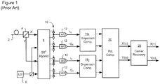
- Fig 1 schematically illustrates a representative coherent optical receiver in which techniques in accordance with the present invention can be implemented.
- an inbound optical signal is received through an optical link 2, split into orthogonal polarizations by a Polarization Beam Splitter 4, and then mixed with a Local Oscillator (LO) signal 6 by a conventional 90° hybrid 8.
- the composite optical signals emerging from the optical hybrid 8 are supplied to respective photodetectors 10, which generate corresponding analog signals.
- the analog photodetector signals are sampled by respective Analog-to-Digital (A/D) converters 12 to yield multi-bit digital sample streams corresponding to In-phase (I) and Quadrature (Q) components of each of the received polarizations.
- A/D Analog-to-Digital
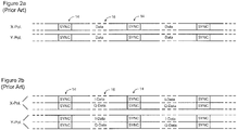
- FIGs. 2a and 2b illustrate representative optical signal formats which may be used in conjunction with embodiments of the present invention.
- the optical signal includes nominally regularly spaced SYNC bursts 14 embedded within a stream of data symbols 16.
- Each SYNC burst 14 has a respective predetermined symbol (or, equivalently, bit) sequence on each transmitted polarization.
- the symbol (bit) sequences of each polarization are preferably transmitted simultaneously, but this is not necessary.
- two orthogonal bit sequences are used in each SYNC burst 14; each bit sequence being assigned to a respective transmitted polarization.
- FIGs. 2a and 2b illustrates an alternative arrangement, in which each of the I and Q components of each transmitted polarization is assigned a respective orthogonal bit sequence.
- the signal formats illustrated in FIGs. 2a and 2b represent signal formats at the transmitter end of the link. Impairments of the optical link distort the transmitted signal such that the polarizations of the light inbound to the receiver will tend to be neither orthogonal nor aligned with the polarization beam splitter 4.
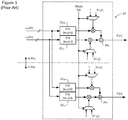
- the I and Q sample streams of each received polarization are supplied to a respective dispersion compensator 18, which operates on the sample stream(s) to compensate chromatic dispersion.
- the dispersion-compensated sample streams appearing at the output of the dispersion compensators 18 are then supplied to a polarization compensator 20 which operates to compensate polarization effects, and thereby de-convolve transmitted symbols from the complex sample streams output from the dispersion compensators 18.
- the polarization compensator 20 may operate as described in Applicant's United States Patent No. 7,555,227 which issued June 30, 2009.
- the polarization compensator 20 is provided as a pair of Finite Impulse Response (FIR) filters 22 for each transmitted polarization.
- FIR Finite Impulse Response
- Each FIR filter 22 is loaded with respective complex tap weights ⁇ X0 (n), ⁇ X1 (n), ⁇ Y0 (n), and ⁇ Y1 (n) which may be computed as described in United States Patent No. 7,555,227 .
- each FIR filter 22 In a Training mode of the receiver, the output of each FIR filter 22 is multiplied by the conjugate of the known SYNC symbols S X (i) and S Y (i), and summed (at 24) to compute respective correlations between the dispersion compensated samples of the SYNC burst 14 and the known SYNC symbols S X (i) and S Y (i), On the other hand, in a data directed mode of the receiver, the FIR outputs are summed (at 24) to generate multi-bit symbol estimates X'(n) and Y'(n) containing both amplitude and phase information of each transmitted symbol.
- the symbol estimates X'(n) and Y'(n) are 10-bit digital values, comprising 5-bits for each of the real and imaginary parts. These estimated symbol values include phase error due to the frequency offset ⁇ f between the Tx and LO frequencies, laser line width and Cross-phase modulation (XPM).
- the polarization compensator 20 outputs are then supplied to a carrier recovery block 26 (see FIG. 1 ), which performs carrier recovery and phase error correction, and symbol determination.
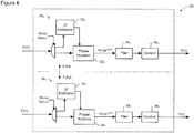
- FIG. 4 schematically illustrates a representative carrier recovery block 26 which performs these operations.
- the carrier recovery block 26 is divided into two substantially identical processing paths 28; one for each transmitted polarization.
- Each processing path 28 receives a respective output of the polarization compensator 20, and outputs recovered symbols of its respective transmitted polarization.
- Each processing path 28 includes a frequency error estimator 30, a phase rotator 32, a filter block 34, and a decision circuit 36.
- each phase rotator 32 uses an estimate of the frequency error generated by the frequency error estimator 30 to compute and apply a phase rotation ⁇ (n) to the symbol estimates received from the polarization compensator 20.
- phase-rotated symbol estimates X'(n)e -j ⁇ (n) and Y'(n)e -j ⁇ (n) generated by the phase rotators 32 are then filtered (at 34) and then processed by the decision circuits 36 to generate the recovered symbol values X(n) and Y(n). Representative embodiments of each of these blocks will be described in greater detail below.
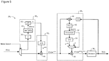
- FIG. 5 schematically illustrates the carrier recovery block 26 of FIG. 4 in greater detail. It will be noted that only the X-Polarization processing path 28 x is illustrated in FIG. 5 , it being understood that a substantially identical arrangement will be provided for the Y-Polarization processing path 28 Y .
- the carrier recovery 26 block of FIG. 5 is configured for two operating modes, namely: a "training" mode while processing a SYNC burst 14; and a "data directed" mode while recovering transmitted data symbols 16.
- the correlation values output by the polarization compensator 20 are supplied to the frequency error estimator 30, which computes a local slope ⁇ as an estimate of the frequency error due to the frequency offset ⁇ f between the transmit laser and the LO and independent laser line width.
- the SYNC burst correlation values output by the polarization compensator 20 are accumulated (at 38) to average the correlation across at least a portion of the SYNC burst 14.
- This SYNC burst phase error estimate represents the average phase error of the symbols comprising the SYNC burst, relative to the ideal phase of those symbols, as determined by the encoding format (e.g. PSK, QPSK, 16-QAM etc.) of the optical signal.
- the symbol estimates of each SYNC burst contain phase errors due to frequency offset ⁇ f, laser linewidth, and XPM.
- Computing an average phase error of each SYNC burst has an effect of low-pass filtering the individual phase errors of the SYNC burst symbols at 42, and so tends to reduce the effects of laser phase noise and XPM.
- FIG. 6 is a chart schematically illustrating phase error ⁇ ⁇ vs. time (shown as dashed line, 44) for a portion of a received signal.
- the phase error ⁇ ⁇ exhibits an unbounded phase ramp 45 due to the frequency errorand short-period phase excursions due to XPM and laser phase noise.
- the local slope ⁇ of the phase ramp 45 represents the frequency error due to the frequency offset ⁇ f between the transmit and LO lasers and independent laser line width, while the short-period phase excursions are bounded and average to zero relative to the phase ramp 45.
- FIG. 6 is a chart schematically illustrating phase error ⁇ ⁇ vs. time (shown as dashed line, 44) for a portion of a received signal.
- the phase error ⁇ ⁇ exhibits an unbounded phase ramp 45 due to the frequency errorand short-period phase excursions due to XPM and laser phase noise.
- the local slope ⁇ of the phase ramp 45 represents the frequency error due to the frequency offset
- phase error estimates ⁇ ⁇ SYNC ( i ) of three successive SYNC bursts are shown, each of which represents the average phase error of the symbol estimates comprising the respective SYNC burst.
- the phase slope ⁇ SYNC ( i ) can be directly used as the local slope ⁇ .
- the phase ramp 45 can be more closely approximated by computing the local slope ⁇ as an average over a suitable number of successive phase slope values, as may be seen in FIG. 6 .
- the number of phase slope values used to calculate the local slope ⁇ can be selected based on the expected variability of the frequency error. In cases where the frequency error changes very slowly in comparison to the repetition rate of the SYNC bursts, a relatively large number of phase slope values can be used to calculate the local slope ⁇ . Alternatively, in cases where the frequency error changes more rapidly, a smaller number of phase slope values may be used to calculate the local slope ⁇ . If desired, operations such as finite impulse response filters, infinite impulse response filters, nonlinear filtering functions, extrapolations, interpolations, curve fits, or splines can be applied to obtain the local slope ⁇ .
- the receiver switches to the data directed mode, during which the data symbol estimates are rotated by the phase rotators 32 in accordance with the local slope ⁇ , and the resulting rotated symbol estimates X'(n)e -j ⁇ (n) and Y'(n)e -j ⁇ (n) filtered (at 34) and processed by the decision circuits 36 to generate the recovered symbol values X(n) and Y(n). This operation will be described in greater detail below.
- phase rotator 34 computes and imposes a phase rotation ⁇ (n) which compensates the unbounded phase errors of the corresponding symbol estimates X'(n) and Y'(n).
- the phase error is unbounded, this arrangement can result in the accumulated phase rotation ⁇ (n+1) rising to an effectively infinite value over a period of time. It can therefore be beneficial to reset the value of the initial phase rotation ⁇ (n 0 ) for each SYNC burst, prior to processing the next data block. This can be accomplished in a number of different ways.
- the initial phase rotation ⁇ (n 0 ) for a given data block can be set equal to the phase error estimate ⁇ ⁇ SYNC ( i ) of the associated SYNC burst.
- the initial phase rotation ⁇ (n 0 ) for a given data block can be calculated from any of: the phase error estimates ⁇ ⁇ SYNC ( i ) of two or more SYNC bursts; the phase slope ⁇ SYNC ( i ); and the local slope ⁇
- a zero symbol phase error corresponds with the ideal phase angle(s) of the symbol values within the phase space of the relevant encoding scheme.
- the boundaries of each decision region of the encoding scheme phase space therefore correspond with known symbol phase error values above and below zero.
- the QPSK encoding scheme phase space is divided into four decision regions (quadrants), each of which has a width of ⁇ /2.
- the rotated symbol estimates X'(n)e -j ⁇ (n) and Y'(n)e -j ⁇ (n) can be filtered by applying a threshold function to the respective symbol phase error values.
- the respective symbol phase error ⁇ ⁇ (n) of each rotated symbol estimate can be compared to the threshold. For values of
- , the rotated symbol estimate may be taken as lying in an adjacent (incorrect) decision region.
- a second or alternative phase rotation ⁇ (n) can be computed and applied to the corresponding rotated phase estimate, such that the resulting rotated symbol estimate X'(n)e -j ⁇ (n) e -j ⁇ (n) , Y'(n)e- j ⁇ (n) e -j ⁇ (n) have a symbol phase error
- This operation has the effect of clipping the symbol phase error ⁇ ⁇ ( n ) to the threshold values ⁇ Th, as may be seen in FIG. 7b .
- this operation is accomplished using a simplified Least Mean Squares (LMS) algorithm.
- LMS Least Mean Squares
- the filter 34 implements a carrier phase detector in which the rotated symbol estimate X'(n)e -j ⁇ (n) and the conjugate of the corresponding recovered symbol value X(n) are multiplied (at 48) to obtain a multi-bit correlation value.
- the computed symbol phase error ⁇ ⁇ X ( n ) is then compared to the threshold at 52, and the comparison result used to calculate the second phase rotation ⁇ (n) at 54 and apply the calculated phase rotation to the rotated symbol estimate X'(n)e -j ⁇ (n) at 56.
- the rotated symbol estimates may be taken as lying in the correct decision region of the encoding scheme phase space, and the residual phase errors (due to XPM) yield excursions of the symbol phase within that decision region.
- the decision block 36 may operate to determine the recovered symbol values X(n) and Y(n) using methods known, for example, from U.S. Patent No. 7,606,498 .
- the local slope ⁇ is derived from the SYNC bursts, which are impervious to cycle slips, the probability of errors in the recovered symbol values X(n) and Y(n) due to cycle slips is very low as compared to prior art methods.
- the bandwidth of the filter block 34 (which implements a carrier phase detector) is preferably selected to track excursions of the symbol phase due to XPM.
- FIG. 9 is a block diagram schematically illustrating a carrier recovery block 26 which is capable of tracking and compensating large scale phase rotations due to XPM.
- the phase rotation ⁇ (n) computed by the phase rotator 32 includes first and second order phase rotation terms.
- ⁇ n + 1 ⁇ n + ⁇ 1 ⁇ + ⁇ 2 ⁇ ⁇ n + 1
- the scaling factors ⁇ 1 , and ⁇ 2 may be programmable, and define the phase adjustment step sizes for each successive data symbol estimate within the data block.
- the first order phase rotation term ⁇ 1 ⁇ is computed as described above with reference to FIGs. 5 and 6 , and compensates the unbounded phase rotation due to the frequency offset ⁇ f between the transmit and LO lasers and independent laser line-width.
- the second order phase rotation term ⁇ 2 ⁇ ⁇ ( n +1) is updated at the symbol rate, and tracks the phase rotations due to laser linewidth and XPM.
- a frequency domain view to this is that the XPM phase noise and the bounded laser linewidth noise are a low pass process, and the second order phase rotation term ⁇ 2 ⁇ ⁇ ( n +1) represents a high pass filter with a bandwidth determined by 2. Integrating the result over the frequency range of the optical signal yields the variance of the residual XPM and laser noise. This is only mathematically valid because the unbounded phase error contributions are compensated by the first order phase rotation term ⁇ 1 ⁇ .
- the symbol phase error ⁇ ⁇ ( n +1) is computed using a simplified Least Mean Squares (LMS) algorithm or IIR filter.
- LMS Least Mean Squares
- the filter block 34 implements a carrier phase detector in which the rotated symbol estimate X'(n)e -j ⁇ (n) and the conjugate of the corresponding recovered symbol value X(n) are multiplied (at 48) to obtain a multi-bit correlation value.
- the first and second order terms ⁇ 1 ⁇ and ⁇ 2 ⁇ ⁇ ( n +1) provide an estimate of the incremental phase change ⁇ ⁇ between the n th and (n+1) th symbols. Accumulating this incremental value ⁇ for each successive data symbol yields the updated phase rotation ⁇ (n+1).
- An advantage of the embodiment of FIG. 9 is that the first and second order terms ⁇ 1 ⁇ and ⁇ 2 ⁇ ⁇ ( n +1)are independently calculated using respective adaptation loops. This enables the response time and bandwidth of each adaptation loop to be optimized for the specific types of phase errors being compensated. More particularly, the bandwidth of the carrier detector (filter 34) can be optimized to facilitate compensation of XPM, while the response of the frequency offset estimator 30 can be optimized to track changes in the frequency offset ⁇ f. Additionally, in the embodiment of FIG. 9 , the phase rotation ⁇ (n) is updated for each symbol to compensate both frequency offset and XPM.
- the first-order phase rotation term ⁇ 1 ⁇ compensates phase errors due to the frequency offset ⁇ f between the carrier and the LO
- the second order phase rotation term ⁇ 1 ⁇ ⁇ (n+1) compensates phase errors due to laser line-width and XPM.
- the first-order phase rotation term ⁇ 1 ⁇ will rotate the symbol phase to lie within the correct decision region of the encoding scheme phase space, and residual phase errors (due to laser line-width and XPM) will yield excursions of the symbol phase within that decision region.
- the decision block 36 may operate to determine the recovered symbol values X(n) and Y(n) in a manner as described in U.S. Patent No. 7,606,498 .
- the phase evolution due to the frequency error between the transmit and LO lasers is modeled using a piece wise linear approximation, in which each segment has a respective constant local slope ⁇ .
- the local slope ⁇ is updated each SYNC burst, during "training mode" operation of the receiver.
- This arrangement is convenient, in that it provides a means of modelling the phase evolution by processing the SYNC bursts, which provides satisfactory performance with simple circuitry.
- the SYNC bursts can be processed using higher order operations such as curve fitting or splines, for example.
- the resulting model (curve of best fit, or cubic spline) can be used to update local slope ⁇ every M symbols, where M ⁇ 1.
- the local slope ⁇ is updated every symbol, which enables tracking and compensation of constantly changing frequency error.
Claims (16)
- Procédé de récupération de symboles de données dans un récepteur cohérent d'un système de communications optiques, ledit procédé comprenant :le calcul d'une rotation de phase κ(n) qui compense un décalage de fréquence Δf entre un laser de transmission et un oscillateur local (LO) du récepteur ;l'application de la rotation de phase κ(n) à une pluralité d'estimations de symboles de données pour générer des estimations de symboles tournées correspondantes ; etle traitement des estimations de symboles tournées en utilisant une fonction de filtrage limitée pour générer des valeurs de décision correspondantes de chaque symbole de données ; le procédé étant caractérisé par :le traitement de deux ou plus de rafales SYNC ayant une séquence et une périodicité connue de symboles telles que l'erreur de phase moyenne de chaque rafale SYNC soit de zéro afin d'en dériver une estimation d'un décalage de fréquence Δf entre un laser de transmission et un oscillateur local (LO) du récepteur;dans lequel la rotation de phase κ(n) est calculée sur la base de l'estimation du décalage de fréquence Δf.
- Procédé selon la revendication 1, dans lequel chaque symbole de données est codé en fonction d'un schéma de codage prédéterminé et dans lequel le schéma de codage prédéterminé n'est pas un schéma de codage différentiel.
- Procédé selon la revendication 1, dans lequel le traitement de deux ou plus de rafales SYNC comprend :le calcul d'une pente de phase ηφ SYNC (i) entre une paire de rafales SYNC successives ; etla dérivation d'un paramètre de décalage de phase ψ sur la base de la pente de phase calculée.
- Procédé selon la revendication 3, dans lequel le calcul de la pente de phase entre une paire de rafales SYNC successives comprend :le calcul d'une erreur de phase respective Δφ SYNC (i) de chaque rafale SYNC par rapport à une phase idéale de valeurs de symboles correspondantes dans un espace de phase d'un schéma de codage utilisé pour coder les symboles de données;le calcul de la pente de phase ηφ SYNC (i) en utilisant les erreurs de phase respectives et la périodicité connue des rafales SYNC.
- Procédé selon la revendication 3, dans lequel le paramètre de décalage de phase ψ est égal à la pente de phase calculée.
- Procédé selon la revendication 3, dans lequel le paramètre de décalage de phase ψ est égal à une moyenne de pentes de phase respectives de deux ou plus de paires successives de rafales SYNC.
- Procédé selon la revendication 3, dans lequel le calcul de la rotation de phase κ(n) comprend l'accumulation pour chaque estimation de symbole de données successive d'une rotation de phase incrémentale correspondante correspondant à µ1ψ, où µ1 est un facteur d'échelle définissant un pas d'ajustement de phase pour chaque estimation de symbole successive.
- Procédé selon la revendication 1, dans lequel le traitement des estimations de symboles tournées comprend pour chaque estimation de symbole tournée :le calcul d'une erreur de phase de symbole respective Δφ(n) de l'estimation de symbole tournée ;le filtrage de l'estimation de symbole tournée sur la base de l'erreur de phase de symbole calculée Δφ(n) ; etla sélection d'une valeur de décision d'un symbole de données correspondant sur la base de l'estimation de symbole filtrée.
- Procédé selon la revendication 8, dans lequel le filtrage de l'estimation de symbole tournée comprend :la comparaison de l'erreur de phase de symbole respective Δφ(n) à un seuil prédéterminé ; et,lorsque l'erreur de phase de symbole respective Δφ(n) dépasse le seuil prédéterminé, l'écrêtage d'une phase de l'estimation de symbole tournée.
- Procédé selon la revendication 9, dans lequel l'écrêtage d'une phase de l'estimation de symbole tournée comprend :le calcul d'une seconde rotation de phase τ(n) sur la base d'une différence entre l'erreur de phase de symbole respective Δφ(n) et le seuil prédéterminé ; etl'application de la seconde rotation de phase τ(n) à l'estimation de symbole tournée.
- Procédé selon la revendication 8, dans lequel la valeur de seuil prédéterminée est basée sur une largeur de régions de décision d'un espace de phase d'un schéma de codage utilisé pour coder les symboles de données.
- Procédé selon la revendication 11, dans lequel la valeur de seuil prédéterminée correspond à un décalage de phase de limites de chaque région de décision par rapport à une phase idéale de symboles du schéma de codage.
- Procédé selon la revendication 11, dans lequel la valeur de seuil prédéterminée diffère d'un décalage de phase de limites de chaque région de décision par rapport à une phase idéale de symboles du schéma de codage.
- Procédé selon la revendication 8, dans lequel la valeur de seuil prédéterminée est basée sur une largeur de bande d'un bloc filtrant du récepteur pour filtrer les estimations de symboles tournées.
- Procédé selon la revendication 8, dans lequel le filtrage de l'estimation de symbole tournée comprend pour chaque estimation de symbole :le calcul d'un terme de rotation de phase du second ordre respectif µ2Δφ(n+1) basé sur l'erreur de phase de symbole Δφ(n), où µ2 est un facteur d'échelle définissant un pas d'ajustement de phase pour chaque estimation de symbole successive ; etl'addition du terme de rotation de phase du second ordre µ2Δφ(n+1) à la rotation de phase κ(n) appliquée à l'estimation de symbole.
- Procédé selon la revendication 8, dans lequel la sélection de la valeur de décision comprend :l'analyse d'une phase de l'estimation de symbole filtrée pour identifier une région de décision d'un espace de phase d'un schéma de codage utilisé pour coder les symboles de données, dans lequel l'estimation de symbole filtrée est située ; etla sélection d'une valeur de symbole du schéma de codage associé à la région de décision identifiée comme valeur de décision.
Priority Applications (1)
| Application Number | Priority Date | Filing Date | Title |
|---|---|---|---|
| EP11170260.1A EP2536040B1 (fr) | 2011-06-16 | 2011-06-16 | Récupération de support à moyenne nulle |
Applications Claiming Priority (1)
| Application Number | Priority Date | Filing Date | Title |
|---|---|---|---|
| EP11170260.1A EP2536040B1 (fr) | 2011-06-16 | 2011-06-16 | Récupération de support à moyenne nulle |
Publications (2)
| Publication Number | Publication Date |
|---|---|
| EP2536040A1 EP2536040A1 (fr) | 2012-12-19 |
| EP2536040B1 true EP2536040B1 (fr) | 2017-01-18 |
Family
ID=44872688
Family Applications (1)
| Application Number | Title | Priority Date | Filing Date |
|---|---|---|---|
| EP11170260.1A Active EP2536040B1 (fr) | 2011-06-16 | 2011-06-16 | Récupération de support à moyenne nulle |
Country Status (1)
| Country | Link |
|---|---|
| EP (1) | EP2536040B1 (fr) |
Families Citing this family (1)
| Publication number | Priority date | Publication date | Assignee | Title |
|---|---|---|---|---|
| US10084621B2 (en) | 2017-02-01 | 2018-09-25 | Qualcomm Incorporated | Clock data recovery with non-uniform clock tracking |
Family Cites Families (6)
| Publication number | Priority date | Publication date | Assignee | Title |
|---|---|---|---|---|
| US5732111A (en) * | 1995-12-06 | 1998-03-24 | Rockwell International Corporation | Frequency error compensation for direct sequence spread spectrum systems |
| US6973150B1 (en) * | 2001-04-24 | 2005-12-06 | Rockwell Collins | Cycle slip detection using low pass filtering |
| US7606498B1 (en) | 2005-10-21 | 2009-10-20 | Nortel Networks Limited | Carrier recovery in a coherent optical receiver |
| US7522841B2 (en) | 2005-10-21 | 2009-04-21 | Nortel Networks Limited | Efficient data transmission and training of data processing functions |
| US7555227B2 (en) | 2005-10-21 | 2009-06-30 | Nortel Networks Limited | Polarization compensation in a coherent optical receiver |
| JP5646609B2 (ja) * | 2009-05-29 | 2014-12-24 | トムソン ライセンシングThomson Licensing | シンボルタイミングリカバリのための方法と装置 |
-
2011
- 2011-06-16 EP EP11170260.1A patent/EP2536040B1/fr active Active
Non-Patent Citations (1)
| Title |
|---|
| None * |
Also Published As
| Publication number | Publication date |
|---|---|
| EP2536040A1 (fr) | 2012-12-19 |
Similar Documents
| Publication | Publication Date | Title |
|---|---|---|
| US8315528B2 (en) | Zero mean carrier recovery | |
| US10396902B2 (en) | Minimum variance carrier recovery with increased phase noise tolerance | |
| US7606498B1 (en) | Carrier recovery in a coherent optical receiver | |
| US7627252B2 (en) | Clock recovery from an optical signal with dispersion impairments | |
| CA2744586C (fr) | Localisation et correction de glissement de cycle | |
| US8929749B2 (en) | Minimum variance carrier recovery | |
| EP1946474B1 (fr) | Transmission de donnees efficace et entrainement de fonctions de traitement des donnees | |
| EP2357740B1 (fr) | Récepteur optique | |
| US8639126B1 (en) | Coarse frequency offset estimation and correction for high-speed optical communications | |
| US20100329677A1 (en) | Symbol Timing Recovery in Polarization Division Multiplexed Coherent Optical Transmission System | |
| US9240843B1 (en) | Method and apparatus for blind time skew compensation for coherent optical receivers | |
| US20100028011A1 (en) | Digital clock and data recovery scheme | |
| WO2014115840A1 (fr) | Dispositif récepteur optique et procédé de réduction du glissement de cycle de phase | |
| US10594406B2 (en) | Pilot-aided digital signal processing for reception of coherent optical communication | |
| US10439732B2 (en) | Receiving device and phase-error compensation method | |
| EP3055936B1 (fr) | Appareil pour caractériser une dispersion chromatique d'un signal reçu optique | |
| KR100653181B1 (ko) | 주파수 옵셋 보상 기능을 가지는 넌코히런트 동기직접변환 수신 장치 | |
| EP2536040B1 (fr) | Récupération de support à moyenne nulle | |
| EP2109272B1 (fr) | Procédé et dispositif de récupération de phase et système de communication comprenant un tel dispositif | |
| US9871597B2 (en) | Apparatus and method for blind LOFO estimation in coherent optical receiver | |
| EP2040398B1 (fr) | Procédé et appareil de détection cohérente de signaux optiques | |
| EP1006700B1 (fr) | Procédé de récupération de porteuse de signal | |
| CA2743524C (fr) | Recuperation de porteuse a moyenne nulle | |
| EP4228174A1 (fr) | Communications optiques classiques et quantiques conjointes | |
| Qi et al. | Multiplier-free carrier phase estimation for low complexity carrier frequency and phase recovery |
Legal Events
| Date | Code | Title | Description |
|---|---|---|---|
| PUAI | Public reference made under article 153(3) epc to a published international application that has entered the european phase |
Free format text: ORIGINAL CODE: 0009012 |
|
| AK | Designated contracting states |
Kind code of ref document: A1 Designated state(s): AL AT BE BG CH CY CZ DE DK EE ES FI FR GB GR HR HU IE IS IT LI LT LU LV MC MK MT NL NO PL PT RO RS SE SI SK SM TR |
|
| AX | Request for extension of the european patent |
Extension state: BA ME |
|
| 17P | Request for examination filed |
Effective date: 20130619 |
|
| RBV | Designated contracting states (corrected) |
Designated state(s): AL AT BE BG CH CY CZ DE DK EE ES FI FR GB GR HR HU IE IS IT LI LT LU LV MC MK MT NL NO PL PT RO RS SE SI SK SM TR |
|
| REG | Reference to a national code |
Ref country code: DE Ref legal event code: R079 Ref document number: 602011034426 Country of ref document: DE Free format text: PREVIOUS MAIN CLASS: H04B0010148000 Ipc: H04B0010610000 |
|
| GRAP | Despatch of communication of intention to grant a patent |
Free format text: ORIGINAL CODE: EPIDOSNIGR1 |
|
| RIC1 | Information provided on ipc code assigned before grant |
Ipc: H04L 27/00 20060101ALI20161004BHEP Ipc: H04B 10/60 20130101ALI20161004BHEP Ipc: H04B 10/61 20130101AFI20161004BHEP |
|
| INTG | Intention to grant announced |
Effective date: 20161028 |
|
| GRAS | Grant fee paid |
Free format text: ORIGINAL CODE: EPIDOSNIGR3 |
|
| GRAA | (expected) grant |
Free format text: ORIGINAL CODE: 0009210 |
|
| AK | Designated contracting states |
Kind code of ref document: B1 Designated state(s): AL AT BE BG CH CY CZ DE DK EE ES FI FR GB GR HR HU IE IS IT LI LT LU LV MC MK MT NL NO PL PT RO RS SE SI SK SM TR |
|
| REG | Reference to a national code |
Ref country code: GB Ref legal event code: FG4D |
|
| REG | Reference to a national code |
Ref country code: CH Ref legal event code: EP |
|
| REG | Reference to a national code |
Ref country code: AT Ref legal event code: REF Ref document number: 863446 Country of ref document: AT Kind code of ref document: T Effective date: 20170215 |
|
| REG | Reference to a national code |
Ref country code: IE Ref legal event code: FG4D |
|
| REG | Reference to a national code |
Ref country code: NL Ref legal event code: FP |
|
| REG | Reference to a national code |
Ref country code: DE Ref legal event code: R096 Ref document number: 602011034426 Country of ref document: DE |
|
| REG | Reference to a national code |
Ref country code: LT Ref legal event code: MG4D |
|
| REG | Reference to a national code |
Ref country code: AT Ref legal event code: MK05 Ref document number: 863446 Country of ref document: AT Kind code of ref document: T Effective date: 20170118 |
|
| REG | Reference to a national code |
Ref country code: FR Ref legal event code: PLFP Year of fee payment: 7 |
|
| PG25 | Lapsed in a contracting state [announced via postgrant information from national office to epo] |
Ref country code: IS Free format text: LAPSE BECAUSE OF FAILURE TO SUBMIT A TRANSLATION OF THE DESCRIPTION OR TO PAY THE FEE WITHIN THE PRESCRIBED TIME-LIMIT Effective date: 20170518 Ref country code: LT Free format text: LAPSE BECAUSE OF FAILURE TO SUBMIT A TRANSLATION OF THE DESCRIPTION OR TO PAY THE FEE WITHIN THE PRESCRIBED TIME-LIMIT Effective date: 20170118 Ref country code: GR Free format text: LAPSE BECAUSE OF FAILURE TO SUBMIT A TRANSLATION OF THE DESCRIPTION OR TO PAY THE FEE WITHIN THE PRESCRIBED TIME-LIMIT Effective date: 20170419 Ref country code: NO Free format text: LAPSE BECAUSE OF FAILURE TO SUBMIT A TRANSLATION OF THE DESCRIPTION OR TO PAY THE FEE WITHIN THE PRESCRIBED TIME-LIMIT Effective date: 20170418 Ref country code: HR Free format text: LAPSE BECAUSE OF FAILURE TO SUBMIT A TRANSLATION OF THE DESCRIPTION OR TO PAY THE FEE WITHIN THE PRESCRIBED TIME-LIMIT Effective date: 20170118 Ref country code: FI Free format text: LAPSE BECAUSE OF FAILURE TO SUBMIT A TRANSLATION OF THE DESCRIPTION OR TO PAY THE FEE WITHIN THE PRESCRIBED TIME-LIMIT Effective date: 20170118 |
|
| PG25 | Lapsed in a contracting state [announced via postgrant information from national office to epo] |
Ref country code: ES Free format text: LAPSE BECAUSE OF FAILURE TO SUBMIT A TRANSLATION OF THE DESCRIPTION OR TO PAY THE FEE WITHIN THE PRESCRIBED TIME-LIMIT Effective date: 20170118 Ref country code: AT Free format text: LAPSE BECAUSE OF FAILURE TO SUBMIT A TRANSLATION OF THE DESCRIPTION OR TO PAY THE FEE WITHIN THE PRESCRIBED TIME-LIMIT Effective date: 20170118 Ref country code: PT Free format text: LAPSE BECAUSE OF FAILURE TO SUBMIT A TRANSLATION OF THE DESCRIPTION OR TO PAY THE FEE WITHIN THE PRESCRIBED TIME-LIMIT Effective date: 20170518 Ref country code: RS Free format text: LAPSE BECAUSE OF FAILURE TO SUBMIT A TRANSLATION OF THE DESCRIPTION OR TO PAY THE FEE WITHIN THE PRESCRIBED TIME-LIMIT Effective date: 20170118 Ref country code: PL Free format text: LAPSE BECAUSE OF FAILURE TO SUBMIT A TRANSLATION OF THE DESCRIPTION OR TO PAY THE FEE WITHIN THE PRESCRIBED TIME-LIMIT Effective date: 20170118 Ref country code: LV Free format text: LAPSE BECAUSE OF FAILURE TO SUBMIT A TRANSLATION OF THE DESCRIPTION OR TO PAY THE FEE WITHIN THE PRESCRIBED TIME-LIMIT Effective date: 20170118 Ref country code: SE Free format text: LAPSE BECAUSE OF FAILURE TO SUBMIT A TRANSLATION OF THE DESCRIPTION OR TO PAY THE FEE WITHIN THE PRESCRIBED TIME-LIMIT Effective date: 20170118 Ref country code: BG Free format text: LAPSE BECAUSE OF FAILURE TO SUBMIT A TRANSLATION OF THE DESCRIPTION OR TO PAY THE FEE WITHIN THE PRESCRIBED TIME-LIMIT Effective date: 20170418 |
|
| REG | Reference to a national code |
Ref country code: DE Ref legal event code: R097 Ref document number: 602011034426 Country of ref document: DE |
|
| PG25 | Lapsed in a contracting state [announced via postgrant information from national office to epo] |
Ref country code: IT Free format text: LAPSE BECAUSE OF FAILURE TO SUBMIT A TRANSLATION OF THE DESCRIPTION OR TO PAY THE FEE WITHIN THE PRESCRIBED TIME-LIMIT Effective date: 20170118 Ref country code: RO Free format text: LAPSE BECAUSE OF FAILURE TO SUBMIT A TRANSLATION OF THE DESCRIPTION OR TO PAY THE FEE WITHIN THE PRESCRIBED TIME-LIMIT Effective date: 20170118 Ref country code: EE Free format text: LAPSE BECAUSE OF FAILURE TO SUBMIT A TRANSLATION OF THE DESCRIPTION OR TO PAY THE FEE WITHIN THE PRESCRIBED TIME-LIMIT Effective date: 20170118 Ref country code: CZ Free format text: LAPSE BECAUSE OF FAILURE TO SUBMIT A TRANSLATION OF THE DESCRIPTION OR TO PAY THE FEE WITHIN THE PRESCRIBED TIME-LIMIT Effective date: 20170118 Ref country code: SK Free format text: LAPSE BECAUSE OF FAILURE TO SUBMIT A TRANSLATION OF THE DESCRIPTION OR TO PAY THE FEE WITHIN THE PRESCRIBED TIME-LIMIT Effective date: 20170118 |
|
| PLBE | No opposition filed within time limit |
Free format text: ORIGINAL CODE: 0009261 |
|
| STAA | Information on the status of an ep patent application or granted ep patent |
Free format text: STATUS: NO OPPOSITION FILED WITHIN TIME LIMIT |
|
| PG25 | Lapsed in a contracting state [announced via postgrant information from national office to epo] |
Ref country code: DK Free format text: LAPSE BECAUSE OF FAILURE TO SUBMIT A TRANSLATION OF THE DESCRIPTION OR TO PAY THE FEE WITHIN THE PRESCRIBED TIME-LIMIT Effective date: 20170118 Ref country code: SM Free format text: LAPSE BECAUSE OF FAILURE TO SUBMIT A TRANSLATION OF THE DESCRIPTION OR TO PAY THE FEE WITHIN THE PRESCRIBED TIME-LIMIT Effective date: 20170118 |
|
| 26N | No opposition filed |
Effective date: 20171019 |
|
| PG25 | Lapsed in a contracting state [announced via postgrant information from national office to epo] |
Ref country code: MC Free format text: LAPSE BECAUSE OF FAILURE TO SUBMIT A TRANSLATION OF THE DESCRIPTION OR TO PAY THE FEE WITHIN THE PRESCRIBED TIME-LIMIT Effective date: 20170118 |
|
| REG | Reference to a national code |
Ref country code: CH Ref legal event code: PL |
|
| PG25 | Lapsed in a contracting state [announced via postgrant information from national office to epo] |
Ref country code: SI Free format text: LAPSE BECAUSE OF FAILURE TO SUBMIT A TRANSLATION OF THE DESCRIPTION OR TO PAY THE FEE WITHIN THE PRESCRIBED TIME-LIMIT Effective date: 20170118 |
|
| REG | Reference to a national code |
Ref country code: IE Ref legal event code: MM4A |
|
| PG25 | Lapsed in a contracting state [announced via postgrant information from national office to epo] |
Ref country code: LI Free format text: LAPSE BECAUSE OF NON-PAYMENT OF DUE FEES Effective date: 20170630 Ref country code: LU Free format text: LAPSE BECAUSE OF NON-PAYMENT OF DUE FEES Effective date: 20170616 Ref country code: IE Free format text: LAPSE BECAUSE OF NON-PAYMENT OF DUE FEES Effective date: 20170616 Ref country code: CH Free format text: LAPSE BECAUSE OF NON-PAYMENT OF DUE FEES Effective date: 20170630 |
|
| REG | Reference to a national code |
Ref country code: BE Ref legal event code: MM Effective date: 20170630 |
|
| REG | Reference to a national code |
Ref country code: FR Ref legal event code: PLFP Year of fee payment: 8 |
|
| PG25 | Lapsed in a contracting state [announced via postgrant information from national office to epo] |
Ref country code: BE Free format text: LAPSE BECAUSE OF NON-PAYMENT OF DUE FEES Effective date: 20170630 |
|
| PG25 | Lapsed in a contracting state [announced via postgrant information from national office to epo] |
Ref country code: MT Free format text: LAPSE BECAUSE OF NON-PAYMENT OF DUE FEES Effective date: 20170616 |
|
| PG25 | Lapsed in a contracting state [announced via postgrant information from national office to epo] |
Ref country code: HU Free format text: LAPSE BECAUSE OF FAILURE TO SUBMIT A TRANSLATION OF THE DESCRIPTION OR TO PAY THE FEE WITHIN THE PRESCRIBED TIME-LIMIT; INVALID AB INITIO Effective date: 20110616 |
|
| PG25 | Lapsed in a contracting state [announced via postgrant information from national office to epo] |
Ref country code: CY Free format text: LAPSE BECAUSE OF NON-PAYMENT OF DUE FEES Effective date: 20170118 |
|
| PG25 | Lapsed in a contracting state [announced via postgrant information from national office to epo] |
Ref country code: MK Free format text: LAPSE BECAUSE OF FAILURE TO SUBMIT A TRANSLATION OF THE DESCRIPTION OR TO PAY THE FEE WITHIN THE PRESCRIBED TIME-LIMIT Effective date: 20170118 |
|
| PG25 | Lapsed in a contracting state [announced via postgrant information from national office to epo] |
Ref country code: TR Free format text: LAPSE BECAUSE OF FAILURE TO SUBMIT A TRANSLATION OF THE DESCRIPTION OR TO PAY THE FEE WITHIN THE PRESCRIBED TIME-LIMIT Effective date: 20170118 |
|
| PG25 | Lapsed in a contracting state [announced via postgrant information from national office to epo] |
Ref country code: AL Free format text: LAPSE BECAUSE OF FAILURE TO SUBMIT A TRANSLATION OF THE DESCRIPTION OR TO PAY THE FEE WITHIN THE PRESCRIBED TIME-LIMIT Effective date: 20170118 |
|
| REG | Reference to a national code |
Ref country code: DE Ref legal event code: R082 Ref document number: 602011034426 Country of ref document: DE |
|
| P01 | Opt-out of the competence of the unified patent court (upc) registered |
Effective date: 20230515 |
|
| PGFP | Annual fee paid to national office [announced via postgrant information from national office to epo] |
Ref country code: NL Payment date: 20230620 Year of fee payment: 13 Ref country code: FR Payment date: 20230627 Year of fee payment: 13 Ref country code: DE Payment date: 20230620 Year of fee payment: 13 |
|
| PGFP | Annual fee paid to national office [announced via postgrant information from national office to epo] |
Ref country code: GB Payment date: 20230622 Year of fee payment: 13 |