EP2535920A2 - High-voltage supply unit for a particle beam device - Google Patents
High-voltage supply unit for a particle beam device Download PDFInfo
- Publication number
- EP2535920A2 EP2535920A2 EP20120172133 EP12172133A EP2535920A2 EP 2535920 A2 EP2535920 A2 EP 2535920A2 EP 20120172133 EP20120172133 EP 20120172133 EP 12172133 A EP12172133 A EP 12172133A EP 2535920 A2 EP2535920 A2 EP 2535920A2
- Authority
- EP
- European Patent Office
- Prior art keywords
- voltage
- supply unit
- voltage supply
- section
- shield
- Prior art date
- Legal status (The legal status is an assumption and is not a legal conclusion. Google has not performed a legal analysis and makes no representation as to the accuracy of the status listed.)
- Withdrawn
Links
- 239000002245 particle Substances 0.000 title claims abstract description 30
- 239000003990 capacitor Substances 0.000 claims abstract description 46
- 238000009413 insulation Methods 0.000 claims description 28
- 239000004020 conductor Substances 0.000 claims description 16
- 238000005259 measurement Methods 0.000 claims description 9
- 238000010894 electron beam technology Methods 0.000 claims description 7
- 238000010884 ion-beam technique Methods 0.000 claims description 3
- 230000001105 regulatory effect Effects 0.000 claims description 3
- 238000000605 extraction Methods 0.000 description 5
- 230000003287 optical effect Effects 0.000 description 5
- 230000005540 biological transmission Effects 0.000 description 3
- 238000009434 installation Methods 0.000 description 3
- 230000007704 transition Effects 0.000 description 3
- 230000033228 biological regulation Effects 0.000 description 2
- 238000003384 imaging method Methods 0.000 description 2
- 230000001681 protective effect Effects 0.000 description 2
- 230000000087 stabilizing effect Effects 0.000 description 2
- 238000010276 construction Methods 0.000 description 1
- 230000003993 interaction Effects 0.000 description 1
- 238000004519 manufacturing process Methods 0.000 description 1
- 230000010355 oscillation Effects 0.000 description 1
- 230000006641 stabilisation Effects 0.000 description 1
- 238000011105 stabilization Methods 0.000 description 1
Images





Classifications
-
- H—ELECTRICITY
- H01—ELECTRIC ELEMENTS
- H01J—ELECTRIC DISCHARGE TUBES OR DISCHARGE LAMPS
- H01J37/00—Discharge tubes with provision for introducing objects or material to be exposed to the discharge, e.g. for the purpose of examination or processing thereof
- H01J37/02—Details
- H01J37/248—Components associated with high voltage supply
Definitions
- the invention relates to a high-voltage supply unit for a particle beam device, and to a particle beam device comprising a high-voltage supply unit of this type.
- Electron beam devices more particularly a scanning electron microscope (SEM) or a transmission electron microscope (TEM) are used for examining objects in order to obtain knowledge regarding the properties and behavior of said objects under specific conditions.
- SEM scanning electron microscope
- TEM transmission electron microscope
- electrons are generated by means of a beam generator.
- the electrons emerge from the beam generator and form an electron beam. They are accelerated to a potential on account of a potential difference between the beam generator and an anode.
- the beam generator is usually supplied with a negative high voltage.
- said voltage is, for example, in the range of (-1) kV to (-30) kV relative to the ground potential.
- the high voltage is, for example, in the range of (-10) kV to (-300) kV relative to the ground potential.
- a measuring device having a resistive voltage divider or a capacitive voltage divider is used.
- the capacitive voltage divider comprises a first capacitor in the form of a high-voltage capacitor and a second capacitor in the form of a measuring capacitor.
- the first capacitor is accommodated in a housing and sheathed with a high-voltage shield.
- the housing and the high-voltage shield have a high weight, however, such that the measuring device provided with the capacitive voltage divider is very heavy.
- the weight of a known measuring device designed for 200 kV is several hundred kilograms.
- Such a high weight makes the handling and the installation of the known measuring device very complicated. In particular, transporting the measuring device to a particle beam device is laborious. Subsequent installation of the known measuring device is therefore possible only with relatively high outlay.
- the high-voltage capacitor used in the known measuring device is expensive to procure.
- the invention is based on the object of providing a high-voltage supply unit comprising a measuring device for measuring fluctuations of a high voltage which is cost-effective and simple to handle.
- this object is achieved by means of a high-voltage supply unit comprising the features of Claim 1.
- a particle beam device comprising a high-voltage supply unit of this type is provided by the features of Claim 14.
- a use of the high-voltage supply unit according to the invention is described by the features of Claim 13. Further features of the invention are evident from the following description, from the following claims and/or from the accompanying figures.
- the invention provides the high-voltage supply unit for a particle beam device.
- the high-voltage supply unit has at least one high-voltage cable for feeding a high voltage. Furthermore, the high-voltage supply unit is provided with at least one measuring device for measuring the high voltage.
- the measuring device has at least one first capacitor.
- the first capacitor is embodied, for example, as a high-voltage capacitor. Furthermore, the first capacitor is formed by at least one first section of the high-voltage cable.
- the invention is based on the surprising insight that the high-voltage cable of the high-voltage supply unit can be used as a capacitor.
- the high-voltage cable itself as an electrical line, has a characteristic variable, namely a capacitance per unit length. This characteristic variable describes the capacitance of the high-voltage cable per unit length.
- the first capacitor Given a suitable choice of the length of the abovementioned first section of the high-voltage cable, the first capacitor has a capacitance that suffices for measuring the high voltage.
- the invention firstly has the advantage that the measuring device is cost-effective to produce on account of the simple production of the first capacitor. Secondly, the measuring device is light in comparison with the prior art. Transport and installation of the high-voltage supply unit are therefore simple. Moreover, considerations have revealed that the first capacitor formed in this way has only little influence on the high voltage to be measured, such that measurements of the high voltage are possible with a high accuracy.
- the high-voltage supply unit additionally or alternative provides for the high-voltage cable to have the following construction.
- the high-voltage cable has at least one internal conductor surrounded by at least one first insulation.
- the first insulation is in turn surrounded by at least one first shield.
- the high-voltage cable described above is, for example, a high-voltage cable having a conductive outer surface.
- the first shield is interrupted in at least one first region and/or in at least one second region of the first section of the high-voltage cable.
- a further embodiment of the high-voltage supply unit additionally or alternatively provides for the first section of the high-voltage cable to extend along a longitudinal axis of the high-voltage cable and furthermore to have a first longitudinal extent. Furthermore, provision is made for the first region to extend along the longitudinal axis of the high-voltage cable with a second longitudinal extent, wherein the second longitudinal extent of the first region is less than the first longitudinal extent of the first section of the high-voltage cable. In addition or as an alternative thereto, provision is made for the second region to extend along the longitudinal axis of the high-voltage cable with a third longitudinal extent, wherein the third longitudinal extent of the second region is less than the first longitudinal extent of the first section of the high-voltage cable.
- An in turn further embodiment of the high-voltage supply unit according to the invention additionally or alternatively provides for the internal conductor to be surrounded by at least one second insulation. This is provided, in particular, when the high-voltage cable has at least two internal conductors.
- the second insulation is surrounded by at least one third shield.
- This embodiment concerns, for example, a high-voltage cable having a plurality of insulated and shielded internal conductors (namely through the second insulation and through the third shield) surrounded by a further insulation (namely the first insulation), which is in turn shielded (namely by the first shield).
- a further embodiment provides for two or more internal conductors each to be surrounded by a second insulation and for these two or more internal conductors then to be surrounded by a common third shield.
- the high-voltage supply unit has at least one of the following features:
- At least one of the first sheathing and the second sheathing is formed from rubber and/or a plastic.
- An in turn further embodiment of the high-voltage supply unit according to the invention additionally or alternatively provides for the first shield to be at ground potential.
- the first shield is not at ground potential in the first section of the high-voltage cable.
- a further embodiment of the high-voltage supply unit according to the invention additionally or alternatively provides for the measuring device to have at least one capacitive voltage divider, wherein the capacitive voltage divider comprises the first capacitor and at least one second capacitor.
- the measuring device to have at least one measuring resistor for measuring the high voltage.
- the measuring resistor is arranged in a voltage measuring unit. The measuring resistor can therefore directly be a part of a voltage measuring unit.
- Yet another embodiment of the high-voltage supply unit according to the invention additionally or alternatively provides for the high-voltage cable to comprise at least one second section.
- the first section is arranged at a distance from the second section.
- These exemplary embodiments provide, for example, for a plurality of first capacitors to be formed on the high-voltage cable. Both the first section and the second section form a first capacitor in each case.
- the invention also relates to a use of a high-voltage supply unit comprising at least one of the abovementioned features or comprising at least two of the abovementioned features for measuring fluctuations of a high voltage and/or for generating a measurement signal used for regulating the high-voltage supply unit.
- the invention furthermore relates to a particle beam device comprising at least one beam generator for generating a particle beam, comprising at least one objective lens for focusing the particle beam onto at least one object, and comprising at least one high-voltage supply unit, wherein the high-voltage supply unit has at least one of the abovementioned features or at least two of the abovementioned features.
- One embodiment of the particle beam device according to the invention additionally or alternatively provides for the high-voltage supply unit to be designed to supply an electron source or an electrode, for example an extraction electrode or an anode, with high voltage.
- the high-voltage supply unit is designed to supply further components of the particle beam device, for example at least one electrode of a corrector or a spectrometer.
- the particle beam device is embodied, for example, as an electron beam device or as an ion beam device.
- the invention is described below on the basis of a particle beam device in the form of a transmission electron microscope (always designated by TEM hereinafter) and a scanning electron microscope (always designated by SEM hereinafter).
- TEM transmission electron microscope
- SEM scanning electron microscope
- the invention is not restricted to a TEM or an SEM. Rather, the invention can be used in any particle beam device, for example also in an ion beam device.
- FIG. 1 shows a schematic illustration of a TEM 11.
- the TEM 11 has an electron source 1 in the form of a thermal field emission source. However, some other electron source can indeed be used as well.
- an extraction electrode 2 is arranged downstream of the electron source 1, electrons being extracted from the electron source 1 by virtue of the potential of said electrode.
- a first electrode 3 for focusing the source position and a second electrode 4 for accelerating the electrons are provided.
- the electrons emerging from the electron source 1 are accelerated to a desired and adjustable energy by means of an electrode voltage.
- the electron source 1 is connected to a high-voltage supply unit 100 via a high-voltage cable 101. This will be discussed in even greater detail further below.
- a multistage condenser which has three magnetic lenses 5 to 7 (namely a first magnetic lens 5, a second magnetic lens 6 and a third magnetic lens 7), said condenser being followed by an objective 8 provided in the form of a magnetic lens.
- An object plane 9 is arranged at the objective 8, at which object plane an object to be examined can be arranged by means of a sample manipulator.
- a diffraction lens 15 embodied as a magnetic lens is disposed downstream of the objective 8 in the opposite direction to the electron source 1.
- the diffraction lens 15 firstly images a back focal plane 10 of the objective 8 into a diffraction intermediate image plane 21.
- the objective 8 generates a real intermediate image 14 of the object plane 9.
- the diffraction lens 15 secondly images the intermediate image 14 of the object plane 9 into the entrance image plane 17 of a projection system consisting of a first projection lens 18 and a second projection lens 19.
- the projection system 18, 19 then generates, from the object arranged in the object plane 9 and imaged into the entrance image plane 17 of the projection system 18, 19, an image on a detector 20.
- a TEM 11 of this type can have further lenses and deflection and correction systems (for example stigmators or correctors) and/or spectrometers.
- FIG. 2 shows a further particle beam device in the form of an SEM 12, on which the invention is realized.
- the particle beam device has an electron column 22, which is provided with an optical axis 23, a beam generator in the form of an electron source 24 (cathode), an extraction electrode 25 and an anode 26, which simultaneously forms one end of a beam guiding tube 27.
- the electron source 24 is a thermal field emitter. Electrons that emerge from the electron source 24 are accelerated to anode potential on account of a potential difference between the electron source 24 and the anode 26. Accordingly, a particle beam in the form of an electron beam is provided.
- the electron source 24 is connected to a high-voltage supply unit 100 via a high-voltage cable 101.
- an objective lens 28 which has a hole through which the beam guiding tube 27 passes.
- the objective lens 28 furthermore has pole shoes 29, in which coils 30 are arranged.
- An electrostatic delay device is connected downstream of the beam guiding tube 27. Said device consists of an individual electrode 31 and a tube electrode 32.
- the tube electrode 32 lies at that end of the beam guiding tube 27 which lies opposite a carrier element 33.
- the carrier element 33 serves for accommodating an object to be examined.
- the tube electrode 32 together with the beam guiding tube 27 is at anode potential, while the individual electrode 31 and an object arranged on the carrier element 33 are at a potential lower than the anode potential. In this way, the electrons of the particle beam can be decelerated to a desired energy required for the examination of an object arranged on the carrier element 33.
- the electron column 22 additionally has scanning means 34, by which the electron beam can be deflected and scanned over an object arranged on the carrier element 33.
- secondary electrons and/or backscattered electrons which arise on account of the interaction of the electron beam with an object arranged on the carrier element 33 are detected by means of a detector 35 arranged in the beam guiding tube 27.
- the signals generated by the detector 35 are communicated to an electronic unit (not illustrated) for imaging purposes.
- FIG. 3 shows a schematic illustration of the prior art which has been used heretofore for measuring the high voltage in the TEM 11 and/or the SEM 12.
- the high-voltage supply unit 100 is connected to the TEM 11 or the SEM 12 via the high-voltage cable 101. It has a high-voltage generator 102, a high-voltage regulator 104 and a resistor 103 for the high-voltage regulator 104.
- the high-voltage regulator 104 and the resistor 103 serve for regulating the high voltage made available by the high-voltage supply unit 100.
- a reference signal is compared with the actual signal obtained via the resistor 103 and the high-voltage regulator 104 sets the high-voltage generator 102 in such a way that the actual signal corresponds to the reference signal.
- a measuring device 105 is provided, which has a high-voltage capacitor 106. The latter is connected to a measuring unit 107 via a tap.
- the measuring device 105 with the high-voltage capacitor 106 can alternatively be directly integrated in the high-voltage supply unit 100 and then does not require a separate housing in this case.
- the measuring unit 107 indicates the fluctuations of the high voltage made available by the high-voltage supply unit 100.
- fluctuations are understood to mean, for example, oscillations in the range of from approximately 1/10 Hz to many 100 kHz (that is to say slow fluctuations (approximately 1/10 Hz) to very high-frequency fluctuations (greater than 100 kHz)).
- This measurement signal of the measuring unit 107 can be utilized for assessing the stability of the high-voltage supply unit 100. Additionally or alternatively, it is also possible to utilize this measurement signal for stabilizing the regulation of the high-voltage supply unit 100.
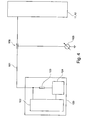
- Figure 4 shows a schematic illustration of a high-voltage supply unit 100 according to the invention.
- Figure 4 is based on figure 3 . Identical components are therefore provided with identical reference signs.
- the invention now provides for the high-voltage cable 101 to have a first section 108, which is embodied as a high-voltage capacitor.
- FIG. 5 shows a schematic illustration of a first embodiment of the high-voltage cable 101, which is constructed symmetrically with respect to a longitudinal axis 116.
- the high-voltage cable 101 has an internal conductor 109, which is surrounded by a first insulation 110.
- the first insulation 110 is in turn surrounded by a first shield 111.
- the high-voltage cable 101 now has the first section 108, which forms the first capacitor.
- the first section 108 of the high-voltage cable 101 has a first end 114 and a second end 115.
- a first region 112 is arranged at the first end 114.
- a second region 113 is arranged at the second end 115.
- the first shield 111 is separated both in the first region 112 and in the second region 113.
- the first shield 111 is interrupted in the first region 112 and in the second region 113. That part 117 of the first shield 111 which is arranged between the first region 112 and the second region 113 forms an electrode of the first section 108 embodied as a first capacitor.
- the first shield 111 is surrounded by a first sheathing 118 over the entire length of the high-voltage cable 101. However, here as well provision is made for the first sheathing 118 to be separated both in the first region 112 and in the second region 113.
- a second sheathing 119 is arranged on the first sheathing 118, said second shield extending along the longitudinal axis 116 both across the first region 112 and across the second region 113.
- the second shield 119 is in turn surrounded with a second sheathing 120. Both the first shield 111 and the second shield 119 are at ground potential and serve to protect persons working with the high-voltage supply unit 100.
- first sheathing 118 and/or the second sheathing 120 are not absolutely necessary for the invention. Some embodiments do not have at least one of the two sheathings mentioned above.
- the high-voltage cable 101 can have in the first section 108, for example, a capacitance per unit length in the range of 10 pF/m to 1000 pF/m, or in the range of 50 pF/m to 500 pF/m, or in the range of 80 pF/m to 250 pF/m.
- Figure 5 also shows two possible types of voltage measurement in a schematic illustration.
- the measuring device 105 has a capacitive voltage divider 121.
- the capacitive voltage divider 121 has the first section 108 embodied as a first capacitor (high-voltage capacitor), and a second capacitor 122 (low-voltage capacitor).
- the voltage dropped across the second capacitor 122 is measured by the measuring unit 107.
- a measuring resistor 123 is provided in the measuring device 105, the voltage dropped across said resistor being measured by means of the measuring unit 107.
- the measuring resistor 123 can be a part of the measuring unit 107; to put it another way, the internal resistance of the measuring unit 107 can directly be the measuring resistor 123.
- Figure 6 shows a further embodiment of the high-voltage cable 101.
- Figure 6 is based on figure 5 . Identical components are provided with identical reference signs.
- the embodiment in figure 6 has a second insulation 124 surrounding the internal conductor 109.
- a plurality of internal conductors 109 are provided in the high-voltage cable 101.
- a third shield 125 is arranged around the second insulation 124.
- a plurality of internal conductors 109 can be provided, wherein each of the individual internal conductors 109 is surrounded in each case by a second insulation 124.
- the high voltage at the measuring unit 107 is measured by means of the measuring device 105.
- a protective circuit (not illustrated) as overvoltage protection of the measuring device 105 in the case of voltage flashovers.
- a diode protective circuit is used, for example, which can additionally also be supplemented by a capacitor circuit and/or a resistor circuit.
- Figure 7 shows an enlarged schematic illustration of the second end 115 of the first section 108 of the high-voltage cable 101.
- Figure 7 is based on figure 5 .
- Identical components are provided with identical reference signs.
- a shapeable insulation 126 is arranged in the second region 113, said insulation completely filling the second region 113 and adjoining the first insulation 110.
- the shapeable insulation 126 adjoins the first shield 111, the second shield 119 and the first sheathing 118.
- the second shield 119 is bent in an S-shape manner at its first end 127 in such a way that the first end 127 of the second shield 119 bears against the first shield 111. Consequently, the first shield 111 and the second shield 119 touch one another. They are therefore electrically connected to one another.
- the electrical contact can also be produced differently, for example by means of a cable connection.
- the second sheathing 120 is led in such a way that it bears against the first sheathing 118 and is then led over the second shield 119.
- This embodiment has the advantage that high field strengths cannot arise at the transition locations of the individual components.
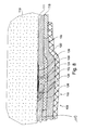
- Figure 8 shows a further enlarged schematic illustration of the second end 115 of the first section 108 of the high-voltage cable 101.
- the exemplary embodiment in figure 8 is based on figure 7 . Identical components are provided with identical reference signs.
- the first shield 111 and that part 117 of the first shield 111 which is arranged between the first region 112 and the second region 113 have a cutout 130 in the boundary region between the first shield 111 and the first insulation 110 and also between the part 117 of the first shield 111 and the first insulation 110.
- a conductive layer 128 is formed in the cutout 130 in the region of the first shield 111, said conductive layer touching a lug 131 of the shapeable insulation 126 and extending as far as the cutout 130 along the part 117 of the first shield 111. Furthermore, at the part 117 of the first shield 111 in the cutout 130, an insulating layer 129 is additionally arranged, which partly covers the conductive layer 128 and likewise adjoins the lug 131 of the shapeable insulation 126. This ensures that the part 117 of the first shield 111 is furthermore insulated from the first shield 111.
- the transition locations are made narrower, that is to say arranged close to one another. This embodiment also has the advantage that high field strengths cannot arise at the transition locations of the individual components.
- the embodiment illustrated in figure 8 is not restricted to the illustrated arrangement of the conductive layer 128 and of the insulating layer 129. Rather, any desired arrangement of the conductive layer 128 and of the insulating layer 129 can be provided. By way of example, the conductive layer 128 and the insulating layer 129 can be embodied in mirror-inverted fashion with respect to the arrangement as illustrated in figure 8 .
- the first section 108 and a second section 132 are arranged on the high-voltage cable 101, wherein the second section 132 can be embodied structurally identically to the first section 108. Both the first section 108 and the second section 132 in each case form a first capacitor (high-voltage capacitor). They can in each case be utilized for high-voltage measurement and for regulation and stabilization of the high-voltage supply unit 100 (cf. figure 4 ).
- the invention is based on the surprising insight that the high-voltage cable 101 of the high-voltage supply unit 100 can be used as a capacitor.
- the high-voltage cable 101 itself has a capacitance per unit length. Given a suitable choice of the length of the first section 108 and/or of the second section 132 of the high-voltage cable 101, the first capacitor has a capacitance that suffices for measuring the high voltage.
Landscapes
- Chemical & Material Sciences (AREA)
- Analytical Chemistry (AREA)
- Measurement Of Current Or Voltage (AREA)
- Measuring Instrument Details And Bridges, And Automatic Balancing Devices (AREA)
- Electron Sources, Ion Sources (AREA)
- Particle Accelerators (AREA)
Abstract
Description
- The invention relates to a high-voltage supply unit for a particle beam device, and to a particle beam device comprising a high-voltage supply unit of this type.
- Electron beam devices, more particularly a scanning electron microscope (SEM) or a transmission electron microscope (TEM) are used for examining objects in order to obtain knowledge regarding the properties and behavior of said objects under specific conditions.
- Both in the case of an SEM and in the case of a TEM, electrons are generated by means of a beam generator. The electrons emerge from the beam generator and form an electron beam. They are accelerated to a potential on account of a potential difference between the beam generator and an anode. For this purpose, the beam generator is usually supplied with a negative high voltage. In the case of an SEM, said voltage is, for example, in the range of (-1) kV to (-30) kV relative to the ground potential. In the case of a TEM, the high voltage is, for example, in the range of (-10) kV to (-300) kV relative to the ground potential.
- In order to achieve examination of an object with a high resolution in the case of the particle beam devices mentioned above, it is desirable for the high voltage made available by a high-voltage supply unit not to be subject to large fluctuations. In order to initiate corresponding measures for stabilizing the high voltage, it is known to measure fluctuations of the high voltage. By way of example, a measuring device having a resistive voltage divider or a capacitive voltage divider is used. The capacitive voltage divider comprises a first capacitor in the form of a high-voltage capacitor and a second capacitor in the form of a measuring capacitor. The first capacitor is accommodated in a housing and sheathed with a high-voltage shield. The housing and the high-voltage shield have a high weight, however, such that the measuring device provided with the capacitive voltage divider is very heavy. By way of example, the weight of a known measuring device designed for 200 kV is several hundred kilograms. Such a high weight makes the handling and the installation of the known measuring device very complicated. In particular, transporting the measuring device to a particle beam device is laborious. Subsequent installation of the known measuring device is therefore possible only with relatively high outlay.
- Furthermore, the high-voltage capacitor used in the known measuring device is expensive to procure.
- The invention is based on the object of providing a high-voltage supply unit comprising a measuring device for measuring fluctuations of a high voltage which is cost-effective and simple to handle.
- According to the invention, this object is achieved by means of a high-voltage supply unit comprising the features of
Claim 1. A particle beam device comprising a high-voltage supply unit of this type is provided by the features ofClaim 14. A use of the high-voltage supply unit according to the invention is described by the features of Claim 13. Further features of the invention are evident from the following description, from the following claims and/or from the accompanying figures. - The invention provides the high-voltage supply unit for a particle beam device. The high-voltage supply unit has at least one high-voltage cable for feeding a high voltage. Furthermore, the high-voltage supply unit is provided with at least one measuring device for measuring the high voltage. The measuring device has at least one first capacitor. The first capacitor is embodied, for example, as a high-voltage capacitor. Furthermore, the first capacitor is formed by at least one first section of the high-voltage cable.
- The invention is based on the surprising insight that the high-voltage cable of the high-voltage supply unit can be used as a capacitor. The high-voltage cable itself, as an electrical line, has a characteristic variable, namely a capacitance per unit length. This characteristic variable describes the capacitance of the high-voltage cable per unit length. Given a suitable choice of the length of the abovementioned first section of the high-voltage cable, the first capacitor has a capacitance that suffices for measuring the high voltage.
- The invention firstly has the advantage that the measuring device is cost-effective to produce on account of the simple production of the first capacitor. Secondly, the measuring device is light in comparison with the prior art. Transport and installation of the high-voltage supply unit are therefore simple. Moreover, considerations have revealed that the first capacitor formed in this way has only little influence on the high voltage to be measured, such that measurements of the high voltage are possible with a high accuracy.
- One embodiment of the high-voltage supply unit according to the invention additionally or alternative provides for the high-voltage cable to have the following construction. The high-voltage cable has at least one internal conductor surrounded by at least one first insulation. The first insulation is in turn surrounded by at least one first shield. The high-voltage cable described above is, for example, a high-voltage cable having a conductive outer surface. The first shield is interrupted in at least one first region and/or in at least one second region of the first section of the high-voltage cable. Furthermore, provision is made for the first section of the high-voltage cable to be surrounded by a second shield. Both the first shield and the second shield serve to protect persons working with the high-voltage supply unit according to the invention.
- A further embodiment of the high-voltage supply unit according to the invention additionally or alternatively provides for the first section of the high-voltage cable to extend along a longitudinal axis of the high-voltage cable and furthermore to have a first longitudinal extent. Furthermore, provision is made for the first region to extend along the longitudinal axis of the high-voltage cable with a second longitudinal extent, wherein the second longitudinal extent of the first region is less than the first longitudinal extent of the first section of the high-voltage cable. In addition or as an alternative thereto, provision is made for the second region to extend along the longitudinal axis of the high-voltage cable with a third longitudinal extent, wherein the third longitudinal extent of the second region is less than the first longitudinal extent of the first section of the high-voltage cable.
- An in turn further embodiment of the high-voltage supply unit according to the invention additionally or alternatively provides for the internal conductor to be surrounded by at least one second insulation. This is provided, in particular, when the high-voltage cable has at least two internal conductors. The second insulation is surrounded by at least one third shield. This embodiment concerns, for example, a high-voltage cable having a plurality of insulated and shielded internal conductors (namely through the second insulation and through the third shield) surrounded by a further insulation (namely the first insulation), which is in turn shielded (namely by the first shield). A further embodiment provides for two or more internal conductors each to be surrounded by a second insulation and for these two or more internal conductors then to be surrounded by a common third shield.
- In a next embodiment of the high-voltage supply unit according to the invention, the high-voltage supply unit has at least one of the following features:
- the first shield is surrounded by at least one first sheathing, or
- in the first section of the high-voltage cable the second shield is surrounded by at least one second sheathing.
- By way of example, at least one of the first sheathing and the second sheathing is formed from rubber and/or a plastic.
- An in turn further embodiment of the high-voltage supply unit according to the invention additionally or alternatively provides for the first shield to be at ground potential. However, the first shield is not at ground potential in the first section of the high-voltage cable. However, provision is additionally or alternatively made for the second shield to be at ground potential.
- Yet another embodiment of the high-voltage supply unit according to the invention additionally or alternatively provides
- for the high-voltage cable to have a capacitance per unit length in the range of 10 pF/m to 1000 pF/m, or
- for the high-voltage cable to have a capacitance per unit length in the range of 50 pF/m to 500 pF/m, or
- for the high-voltage cable to have a capacitance per unit length in the range of 80 pF/m to 250 pF/m.
- It is expressly pointed out that the invention is not restricted to the values mentioned above. Rather, any suitable value of a capacitance per unit length can be chosen.
- A further embodiment of the high-voltage supply unit according to the invention additionally or alternatively provides for the measuring device to have at least one capacitive voltage divider, wherein the capacitive voltage divider comprises the first capacitor and at least one second capacitor. As an alternative thereto, provision is made, for example, for the measuring device to have at least one measuring resistor for measuring the high voltage. By way of example, the measuring resistor is arranged in a voltage measuring unit. The measuring resistor can therefore directly be a part of a voltage measuring unit.
- Yet another embodiment of the high-voltage supply unit according to the invention additionally or alternatively provides for the high-voltage cable to comprise at least one second section. The first section is arranged at a distance from the second section. By way of example, provision is made for the second section to be embodied identically to the first section. These exemplary embodiments provide, for example, for a plurality of first capacitors to be formed on the high-voltage cable. Both the first section and the second section form a first capacitor in each case.
- The invention also relates to a use of a high-voltage supply unit comprising at least one of the abovementioned features or comprising at least two of the abovementioned features for measuring fluctuations of a high voltage and/or for generating a measurement signal used for regulating the high-voltage supply unit.
- The invention furthermore relates to a particle beam device comprising at least one beam generator for generating a particle beam, comprising at least one objective lens for focusing the particle beam onto at least one object, and comprising at least one high-voltage supply unit, wherein the high-voltage supply unit has at least one of the abovementioned features or at least two of the abovementioned features.
- One embodiment of the particle beam device according to the invention additionally or alternatively provides for the high-voltage supply unit to be designed to supply an electron source or an electrode, for example an extraction electrode or an anode, with high voltage. In addition or as an alternative thereto, provision is made for the high-voltage supply unit to be designed to supply further components of the particle beam device, for example at least one electrode of a corrector or a spectrometer. Furthermore, the particle beam device is embodied, for example, as an electron beam device or as an ion beam device.
- The invention is explained in greater detail below on the basis of exemplary embodiments by means of figures, in which:
-
figure 1 shows a schematic illustration of a particle beam device in the form of a transmission electron microscope; -
figure 2 shows a schematic illustration of a particle beam device in the form of a scanning electron microscope; -
figure 3 shows a schematic illustration of a high-voltage supply unit with measuring device according to the prior art; -
figure 4 shows a schematic illustration of a high-voltage supply unit with measuring device according to the invention; -
figure 5 shows a schematic illustration of a first embodiment of a high-voltage cable embodied as a capacitor; -
figure 6 shows a schematic illustration of a second embodiment of a high-voltage cable embodied as a capacitor; -
figure 7 shows a schematic illustration of an enlarged section of a third embodiment of a high-voltage cable embodied as a capacitor; -
figure 8 shows a schematic illustration of an enlarged section of a fourth embodiment of a high-voltage cable embodied as a capacitor; and -
figure 9 shows a schematic illustration of a high-voltage cable having two first capacitors. - The invention is described below on the basis of a particle beam device in the form of a transmission electron microscope (always designated by TEM hereinafter) and a scanning electron microscope (always designated by SEM hereinafter). However, at this juncture already it is pointed out that the invention is not restricted to a TEM or an SEM. Rather, the invention can be used in any particle beam device, for example also in an ion beam device.
-
Figure 1 shows a schematic illustration of aTEM 11. TheTEM 11 has anelectron source 1 in the form of a thermal field emission source. However, some other electron source can indeed be used as well. Along the optical axis OA of theTEM 11, anextraction electrode 2 is arranged downstream of theelectron source 1, electrons being extracted from theelectron source 1 by virtue of the potential of said electrode. Furthermore, afirst electrode 3 for focusing the source position and a second electrode 4 for accelerating the electrons are provided. On account of the second electrode 4, the electrons emerging from theelectron source 1 are accelerated to a desired and adjustable energy by means of an electrode voltage. For this purpose, theelectron source 1 is connected to a high-voltage supply unit 100 via a high-voltage cable 101. This will be discussed in even greater detail further below. - In the further course on the optical axis OA, a multistage condenser is arranged which has three magnetic lenses 5 to 7 (namely a first magnetic lens 5, a second
magnetic lens 6 and a third magnetic lens 7), said condenser being followed by an objective 8 provided in the form of a magnetic lens. Anobject plane 9 is arranged at theobjective 8, at which object plane an object to be examined can be arranged by means of a sample manipulator. Through corresponding setting of the operating parameters (for example of a lens current) of the first magnetic lens 5, of the secondmagnetic lens 6, of the thirdmagnetic lens 7 and of theobjective 8, in particular the illuminated field of theobject plane 9 can be set. - A
diffraction lens 15 embodied as a magnetic lens is disposed downstream of theobjective 8 in the opposite direction to theelectron source 1. Thediffraction lens 15 firstly images a backfocal plane 10 of theobjective 8 into a diffractionintermediate image plane 21. Furthermore, theobjective 8 generates a realintermediate image 14 of theobject plane 9. Thediffraction lens 15 secondly images theintermediate image 14 of theobject plane 9 into theentrance image plane 17 of a projection system consisting of afirst projection lens 18 and asecond projection lens 19. Theprojection system object plane 9 and imaged into theentrance image plane 17 of theprojection system detector 20. By correspondingly switching over theprojection system focal plane 10 or the diffractionintermediate image plane 21 onto the detector 20 (or into an end image plane). ATEM 11 of this type can have further lenses and deflection and correction systems (for example stigmators or correctors) and/or spectrometers. -
Figure 2 shows a further particle beam device in the form of anSEM 12, on which the invention is realized. The particle beam device has anelectron column 22, which is provided with anoptical axis 23, a beam generator in the form of an electron source 24 (cathode), anextraction electrode 25 and ananode 26, which simultaneously forms one end of abeam guiding tube 27. By way of example, theelectron source 24 is a thermal field emitter. Electrons that emerge from theelectron source 24 are accelerated to anode potential on account of a potential difference between theelectron source 24 and theanode 26. Accordingly, a particle beam in the form of an electron beam is provided. In this exemplary embodiment, too, theelectron source 24 is connected to a high-voltage supply unit 100 via a high-voltage cable 101. - Furthermore, an
objective lens 28 is provided, which has a hole through which thebeam guiding tube 27 passes. Theobjective lens 28 furthermore haspole shoes 29, in which coils 30 are arranged. An electrostatic delay device is connected downstream of thebeam guiding tube 27. Said device consists of anindividual electrode 31 and atube electrode 32. Thetube electrode 32 lies at that end of thebeam guiding tube 27 which lies opposite acarrier element 33. Thecarrier element 33 serves for accommodating an object to be examined. - The
tube electrode 32 together with thebeam guiding tube 27 is at anode potential, while theindividual electrode 31 and an object arranged on thecarrier element 33 are at a potential lower than the anode potential. In this way, the electrons of the particle beam can be decelerated to a desired energy required for the examination of an object arranged on thecarrier element 33. Theelectron column 22 additionally has scanning means 34, by which the electron beam can be deflected and scanned over an object arranged on thecarrier element 33. - For imaging purposes, secondary electrons and/or backscattered electrons which arise on account of the interaction of the electron beam with an object arranged on the
carrier element 33 are detected by means of adetector 35 arranged in thebeam guiding tube 27. The signals generated by thedetector 35 are communicated to an electronic unit (not illustrated) for imaging purposes. -
Figure 3 shows a schematic illustration of the prior art which has been used heretofore for measuring the high voltage in theTEM 11 and/or theSEM 12. The high-voltage supply unit 100 is connected to theTEM 11 or theSEM 12 via the high-voltage cable 101. It has a high-voltage generator 102, a high-voltage regulator 104 and aresistor 103 for the high-voltage regulator 104. The high-voltage regulator 104 and theresistor 103 serve for regulating the high voltage made available by the high-voltage supply unit 100. In this case, by way of example, in the high-voltage regulator 104, a reference signal is compared with the actual signal obtained via theresistor 103 and the high-voltage regulator 104 sets the high-voltage generator 102 in such a way that the actual signal corresponds to the reference signal. In order to measure the high voltage, a measuringdevice 105 is provided, which has a high-voltage capacitor 106. The latter is connected to ameasuring unit 107 via a tap. The measuringdevice 105 with the high-voltage capacitor 106 can alternatively be directly integrated in the high-voltage supply unit 100 and then does not require a separate housing in this case. - The measuring
unit 107 indicates the fluctuations of the high voltage made available by the high-voltage supply unit 100. In this case, fluctuations are understood to mean, for example, oscillations in the range of from approximately 1/10 Hz to many 100 kHz (that is to say slow fluctuations (approximately 1/10 Hz) to very high-frequency fluctuations (greater than 100 kHz)). This measurement signal of the measuringunit 107 can be utilized for assessing the stability of the high-voltage supply unit 100. Additionally or alternatively, it is also possible to utilize this measurement signal for stabilizing the regulation of the high-voltage supply unit 100. -
Figure 4 shows a schematic illustration of a high-voltage supply unit 100 according to the invention.Figure 4 is based onfigure 3 . Identical components are therefore provided with identical reference signs. In contrast to the prior art, the invention now provides for the high-voltage cable 101 to have afirst section 108, which is embodied as a high-voltage capacitor. -
Figure 5 shows a schematic illustration of a first embodiment of the high-voltage cable 101, which is constructed symmetrically with respect to alongitudinal axis 116. The high-voltage cable 101 has aninternal conductor 109, which is surrounded by afirst insulation 110. Thefirst insulation 110 is in turn surrounded by afirst shield 111. The high-voltage cable 101 now has thefirst section 108, which forms the first capacitor. - The
first section 108 of the high-voltage cable 101 has afirst end 114 and asecond end 115. Afirst region 112 is arranged at thefirst end 114. By contrast, asecond region 113 is arranged at thesecond end 115. Thefirst shield 111 is separated both in thefirst region 112 and in thesecond region 113. To put it another way, thefirst shield 111 is interrupted in thefirst region 112 and in thesecond region 113. Thatpart 117 of thefirst shield 111 which is arranged between thefirst region 112 and thesecond region 113 forms an electrode of thefirst section 108 embodied as a first capacitor. - The
first shield 111 is surrounded by afirst sheathing 118 over the entire length of the high-voltage cable 101. However, here as well provision is made for thefirst sheathing 118 to be separated both in thefirst region 112 and in thesecond region 113. In thefirst section 108, asecond sheathing 119 is arranged on thefirst sheathing 118, said second shield extending along thelongitudinal axis 116 both across thefirst region 112 and across thesecond region 113. Thesecond shield 119 is in turn surrounded with asecond sheathing 120. Both thefirst shield 111 and thesecond shield 119 are at ground potential and serve to protect persons working with the high-voltage supply unit 100. - It is explicitly pointed out that the
first sheathing 118 and/or thesecond sheathing 120 are not absolutely necessary for the invention. Some embodiments do not have at least one of the two sheathings mentioned above. - The high-
voltage cable 101 can have in thefirst section 108, for example, a capacitance per unit length in the range of 10 pF/m to 1000 pF/m, or in the range of 50 pF/m to 500 pF/m, or in the range of 80 pF/m to 250 pF/m. -
Figure 5 also shows two possible types of voltage measurement in a schematic illustration. In a first measurement type A, the measuringdevice 105 has acapacitive voltage divider 121. Thecapacitive voltage divider 121 has thefirst section 108 embodied as a first capacitor (high-voltage capacitor), and a second capacitor 122 (low-voltage capacitor). The voltage dropped across thesecond capacitor 122 is measured by the measuringunit 107. In a second measurement type B, a measuringresistor 123 is provided in themeasuring device 105, the voltage dropped across said resistor being measured by means of the measuringunit 107. Additionally or alternatively, the measuringresistor 123 can be a part of the measuringunit 107; to put it another way, the internal resistance of the measuringunit 107 can directly be the measuringresistor 123. -
Figure 6 shows a further embodiment of the high-voltage cable 101.Figure 6 is based onfigure 5 . Identical components are provided with identical reference signs. In contrast to the exemplary embodiment infigure 5 , the embodiment infigure 6 has asecond insulation 124 surrounding theinternal conductor 109. Alternatively, a plurality ofinternal conductors 109 are provided in the high-voltage cable 101. Athird shield 125 is arranged around thesecond insulation 124. In a further exemplary embodiment, a plurality ofinternal conductors 109 can be provided, wherein each of the individualinternal conductors 109 is surrounded in each case by asecond insulation 124. Alternatively, provision is made for all of theinternal conductors 109 to be surrounded by a commonthird shield 125. The high voltage at the measuringunit 107 is measured by means of the measuringdevice 105. In addition, provision can be made of a protective circuit (not illustrated) as overvoltage protection of the measuringdevice 105 in the case of voltage flashovers. For this purpose, a diode protective circuit is used, for example, which can additionally also be supplemented by a capacitor circuit and/or a resistor circuit. -
Figure 7 shows an enlarged schematic illustration of thesecond end 115 of thefirst section 108 of the high-voltage cable 101.Figure 7 is based onfigure 5 . Identical components are provided with identical reference signs. Ashapeable insulation 126 is arranged in thesecond region 113, said insulation completely filling thesecond region 113 and adjoining thefirst insulation 110. Furthermore, theshapeable insulation 126 adjoins thefirst shield 111, thesecond shield 119 and thefirst sheathing 118. Thesecond shield 119 is bent in an S-shape manner at itsfirst end 127 in such a way that thefirst end 127 of thesecond shield 119 bears against thefirst shield 111. Consequently, thefirst shield 111 and thesecond shield 119 touch one another. They are therefore electrically connected to one another. The electrical contact can also be produced differently, for example by means of a cable connection. Thesecond sheathing 120 is led in such a way that it bears against thefirst sheathing 118 and is then led over thesecond shield 119. This embodiment has the advantage that high field strengths cannot arise at the transition locations of the individual components. -
Figure 8 shows a further enlarged schematic illustration of thesecond end 115 of thefirst section 108 of the high-voltage cable 101. The exemplary embodiment infigure 8 is based onfigure 7 . Identical components are provided with identical reference signs. In contrast to the exemplary embodiment infigure 7 , in the exemplary embodiment infigure 8 , thefirst shield 111 and thatpart 117 of thefirst shield 111 which is arranged between thefirst region 112 and thesecond region 113 have acutout 130 in the boundary region between thefirst shield 111 and thefirst insulation 110 and also between thepart 117 of thefirst shield 111 and thefirst insulation 110. Aconductive layer 128 is formed in thecutout 130 in the region of thefirst shield 111, said conductive layer touching alug 131 of theshapeable insulation 126 and extending as far as thecutout 130 along thepart 117 of thefirst shield 111. Furthermore, at thepart 117 of thefirst shield 111 in thecutout 130, an insulatinglayer 129 is additionally arranged, which partly covers theconductive layer 128 and likewise adjoins thelug 131 of theshapeable insulation 126. This ensures that thepart 117 of thefirst shield 111 is furthermore insulated from thefirst shield 111. In this embodiment, the transition locations are made narrower, that is to say arranged close to one another. This embodiment also has the advantage that high field strengths cannot arise at the transition locations of the individual components. - It is pointed out that the embodiment illustrated in
figure 8 is not restricted to the illustrated arrangement of theconductive layer 128 and of the insulatinglayer 129. Rather, any desired arrangement of theconductive layer 128 and of the insulatinglayer 129 can be provided. By way of example, theconductive layer 128 and the insulatinglayer 129 can be embodied in mirror-inverted fashion with respect to the arrangement as illustrated infigure 8 . - The embodiments illustrated in
figures 8 and7 can also be provided for thefirst region 112 of thefirst section 108. - In an embodiment illustrated in
figure 9 , thefirst section 108 and asecond section 132 are arranged on the high-voltage cable 101, wherein thesecond section 132 can be embodied structurally identically to thefirst section 108. Both thefirst section 108 and thesecond section 132 in each case form a first capacitor (high-voltage capacitor). They can in each case be utilized for high-voltage measurement and for regulation and stabilization of the high-voltage supply unit 100 (cf.figure 4 ). - The invention is based on the surprising insight that the high-
voltage cable 101 of the high-voltage supply unit 100 can be used as a capacitor. The high-voltage cable 101 itself has a capacitance per unit length. Given a suitable choice of the length of thefirst section 108 and/or of thesecond section 132 of the high-voltage cable 101, the first capacitor has a capacitance that suffices for measuring the high voltage. -
- 1
- Electron source
- 2
- Extraction electrode
- 3
- First electrode
- 4
- Second electrode
- 5
- First magnetic lens
- 6
- Second magnetic lens
- 7
- Third magnetic lens
- 8
- Objective
- 9
- Objective plane
- 10
- Back focal plane
- 11
- TEM
- 12
- SEM
- 13
- 14
- Real intermediate image
- 15
- Diffraction lens
- 16
- 17
- Entrance image plane for projection lenses
- 18
- First projection lens
- 19
- Second projection lens
- 20
- Detector/end image plane
- 21
- Diffraction intermediate image plane
- 22
- Electron column
- 23
- Optical axis
- 24
- Electron source
- 25
- Extraction electrode
- 26
- Anode
- 27
- Beam guiding tube
- 28
- Objective lens
- 29
- Pole shoes
- 30
- Coils
- 31
- Individual electrode
- 32
- Tube electrode
- 33
- Carrier element
- 34
- Scanning means
- 35
- Detector
- 100
- High-voltage supply unit
- 101
- High-voltage cable
- 102
- High-voltage generator
- 103
- Resistor
- 104
- High-voltage regulator
- 105
- Measuring device
- 106
- High-voltage capacitor
- 107
- Measuring unit
- 108
- First section of the high-voltage cable
- 109
- Internal conductor
- 110
- First insulation
- 111
- First shield
- 112
- First region
- 113
- Second region
- 114
- First end
- 115
- Second end
- 116
- Longitudinal axis
- 117
- Part of the first shield
- 118
- First sheathing
- 119
- Second shield
- 120
- Second sheathing
- 121
- Capacitive voltage divider
- 122
- Second capacitor
- 123
- Measuring resistor
- 124
- Second insulation
- 125
- Third shield
- 126
- Shapeable insulation
- 127
- First end of the second shield
- 128
- Conductive layer
- 129
- Insulating layer
- 130
- Cutout
- 131
- Lug
- 132
- Second section of the high-voltage cable
- OA
- Optical axis
Claims (16)
- High-voltage supply unit (100) for a particle beam device (11, 12), comprising- at least one high-voltage cable (101) for feeding a high voltage, and comprising- at least one measuring device (105) for measuring the high voltage, wherein the measuring device (105) has at least one first capacitor (108, 132),wherein
the first capacitor is formed by at least one first section (108) of the high-voltage cable (101). - High-voltage supply unit (100) according to Claim 1,
wherein- the high-voltage cable (101) has at least one internal conductor (109),- the internal conductor (109) is surrounded by at least one first insulation (110),- the first insulation (110) is surrounded by at least one first shield (111),- the first shield (111) is interrupted in at least one first region (112) and/or in at least one second region (113) of the first section (108) of the high-voltage cable (101), andwherein- the first section (108) of the high-voltage cable (101) is surrounded by at least one second shield (119). - High-voltage supply unit (100) according to Claim 2, wherein the first section (108) of the high-voltage cable (101) extends along a longitudinal axis (116) of the high-voltage cable (101) and has a first longitudinal extent, and wherein- the first region (112) extends along the longitudinal axis (116) of the high-voltage cable (101) with a second longitudinal extent, wherein the second longitudinal extent of the first region (112) is less than the first longitudinal extent of the first section (108) of the high-voltage cable (101) and/or wherein- the second region (113) extends along the longitudinal axis (116) of the high-voltage cable (101) with a third longitudinal extent, wherein the third longitudinal extent of the second region (113) is less than the first longitudinal extent of the first section (108) of the high-voltage cable (101).
- High-voltage supply unit (100) according to Claim 2 or 3, wherein- the internal conductor (109) is surrounded by at least one second insulation (124), and wherein- the second insulation (124) is surrounded by at least one third shield (125).
- High-voltage supply unit (100) according to any of Claims 2 to 4, wherein the high-voltage supply unit (100) has at least one of the following features:- the first shield (111) is surrounded by at least one first sheathing (118), or- in the first section (108) of the high-voltage cable (101) the second shield (119) is surrounded by at least one second sheathing (120).
- High-voltage supply unit (100) according to any of Claims 2 to 5, wherein- the first shield (111) is at ground potential, and/or- the second shield (119) is at ground potential.
- High-voltage supply unit (100) according to any of the preceding claims, wherein- the high-voltage cable (101) has a capacitance per unit length in the range of 10 pF/m to 1000 pF/m, or- the high-voltage cable (101) has a capacitance per unit length in the range of 50 pF/m to 500 pF/m, or- the high-voltage cable (101) has a capacitance per unit length in the range of 80 pF/m to 250 pF/m.
- High-voltage supply unit (100) according to any of the preceding claims, wherein the measuring device (105) has at least one capacitive voltage divider (121), wherein the capacitive voltage divider (121) comprises the first capacitor (108) and at least one second capacitor (122).
- High-voltage supply unit (100) according to any of the preceding claims, wherein the measuring device (105) has at least one measuring resistor (123) for measuring the high voltage.
- High-voltage supply unit (100) according to Claim 9, wherein the measuring resistor is arranged in a voltage measuring unit (107).
- High-voltage supply unit (100) according to any of the preceding claims, wherein- the high-voltage cable (101) comprises at least one second section (132), and wherein- the first section (108) is at a distance from the second section (132).
- High-voltage supply unit (100) according to Claim 11, wherein the second section (132) is embodied identically to the first section (108).
- Use of a high-voltage supply unit (100) according to any of the preceding claims for measuring fluctuations of a high voltage and/or for generating a measurement signal used for regulating the high-voltage supply unit (100).
- Particle beam device (11, 12), comprising- at least one beam generator (1, 24) for generating a particle beam,- at least one objective lens (8, 28) for focusing the particle beam onto at least one object, and- at least one high-voltage supply unit (100) according to any of the preceding Claims 1 to 12.
- Particle beam device (11, 12) according to Claim 14, wherein the high-voltage supply unit (100) is designed to supply the beam generator (1, 24) with high voltage.
- Particle beam device (11, 12) according to Claim 14 or 15, wherein the particle beam device is embodied as an electron beam device or as an ion beam device.
Applications Claiming Priority (1)
| Application Number | Priority Date | Filing Date | Title |
|---|---|---|---|
| DE102011077635A DE102011077635A1 (en) | 2011-06-16 | 2011-06-16 | High voltage power supply unit for a particle beam device |
Publications (2)
| Publication Number | Publication Date |
|---|---|
| EP2535920A2 true EP2535920A2 (en) | 2012-12-19 |
| EP2535920A3 EP2535920A3 (en) | 2015-03-04 |
Family
ID=46845581
Family Applications (1)
| Application Number | Title | Priority Date | Filing Date |
|---|---|---|---|
| EP20120172133 Withdrawn EP2535920A3 (en) | 2011-06-16 | 2012-06-15 | High-voltage supply unit for a particle beam device |
Country Status (5)
| Country | Link |
|---|---|
| US (1) | US8759800B2 (en) |
| EP (1) | EP2535920A3 (en) |
| JP (1) | JP2013016479A (en) |
| CN (1) | CN102832093A (en) |
| DE (1) | DE102011077635A1 (en) |
Families Citing this family (5)
| Publication number | Priority date | Publication date | Assignee | Title |
|---|---|---|---|---|
| DE102010056337A1 (en) * | 2010-12-27 | 2012-06-28 | Carl Zeiss Nts Gmbh | Particle beam system for recording of energy loss spectrum, has high voltage source for providing high voltage between two high voltage outputs and control signal |
| US8952326B1 (en) * | 2013-11-04 | 2015-02-10 | Agilent Technologies, Inc. | Atmospheric pressure interface with improved ion transfer for spectrometry, and related systems and methods |
| DE102018131614B3 (en) * | 2018-12-10 | 2020-02-06 | Carl Zeiss Microscopy Gmbh | Particle beam system and method for operating a particle beam system |
| CN115862274B (en) * | 2023-03-03 | 2023-05-16 | 安标国家矿用产品安全标志中心有限公司 | Multi-band radio frequency electromagnetic energy explosion-proof ignition test device and method |
| CN117219482B (en) * | 2023-11-07 | 2024-01-26 | 国仪量子(合肥)技术有限公司 | Current detection device and scanning electron microscope |
Family Cites Families (17)
| Publication number | Priority date | Publication date | Assignee | Title |
|---|---|---|---|---|
| US3280246A (en) * | 1965-02-02 | 1966-10-18 | Thomas & Betts Corp | Ground sheath connector |
| US3484679A (en) * | 1966-10-03 | 1969-12-16 | North American Rockwell | Electrical apparatus for changing the effective capacitance of a cable |
| US4020318A (en) * | 1975-01-24 | 1977-04-26 | The Welding Institute | Electron beam generators |
| DE2819165A1 (en) * | 1978-05-02 | 1979-11-15 | Siemens Ag | SCANNING ELECTRON MICROSCOPE |
| US4306272A (en) * | 1979-09-18 | 1981-12-15 | Spire Corporation | Tubular capacitor |
| US4281360A (en) * | 1979-12-17 | 1981-07-28 | General Electric Company | High-voltage capacitor |
| JPS56122963A (en) * | 1980-03-04 | 1981-09-26 | Hitachi Cable Ltd | Measuring device for partial discharge |
| DE3702735A1 (en) * | 1987-01-30 | 1988-08-11 | Josef Dipl Ing Trott | Capacitive voltage divider for high-voltage cables |
| US5107201A (en) * | 1990-12-11 | 1992-04-21 | Ogle John S | High voltage oscilloscope probe with wide frequency response |
| DE4436305A1 (en) * | 1994-10-11 | 1996-04-25 | Siemens Ag | X-ray tube high voltage measuring appts. |
| EP0969493A1 (en) * | 1998-07-03 | 2000-01-05 | ICT Integrated Circuit Testing Gesellschaft für Halbleiterprüftechnik mbH | Apparatus and method for examining specimen with a charged particle beam |
| JP4610182B2 (en) * | 2003-12-05 | 2011-01-12 | 株式会社日立ハイテクノロジーズ | Scanning electron microscope |
| JP4262184B2 (en) * | 2004-10-12 | 2009-05-13 | 株式会社日立ハイテクノロジーズ | Transmission electron microscope and image observation method using the same |
| JP4636897B2 (en) * | 2005-02-18 | 2011-02-23 | 株式会社日立ハイテクサイエンスシステムズ | Scanning electron microscope |
| JP4881661B2 (en) * | 2006-06-20 | 2012-02-22 | 株式会社日立ハイテクノロジーズ | Charged particle beam equipment |
| FR2909251B1 (en) * | 2006-11-28 | 2009-01-16 | Gen Electric | HIGH VOLTAGE GENERATOR OF X-RAY APPARATUS HAVING A HIGH VOLTAGE MEASURING DEVICE |
| US8390152B2 (en) | 2009-03-06 | 2013-03-05 | Carl Zeiss Nts Gmbh | Device and method for generating a stable high voltage |
-
2011
- 2011-06-16 DE DE102011077635A patent/DE102011077635A1/en not_active Withdrawn
-
2012
- 2012-06-14 US US13/523,169 patent/US8759800B2/en not_active Expired - Fee Related
- 2012-06-15 EP EP20120172133 patent/EP2535920A3/en not_active Withdrawn
- 2012-06-15 JP JP2012136233A patent/JP2013016479A/en active Pending
- 2012-06-18 CN CN2012102046782A patent/CN102832093A/en active Pending
Also Published As
| Publication number | Publication date |
|---|---|
| JP2013016479A (en) | 2013-01-24 |
| US20120318975A1 (en) | 2012-12-20 |
| DE102011077635A1 (en) | 2012-12-20 |
| US8759800B2 (en) | 2014-06-24 |
| CN102832093A (en) | 2012-12-19 |
| EP2535920A3 (en) | 2015-03-04 |
Similar Documents
| Publication | Publication Date | Title |
|---|---|---|
| US9536703B2 (en) | Scanning electron microscope | |
| US9431210B2 (en) | Charged particle beam device with dynamic focus and method of operating thereof | |
| US10546717B2 (en) | High-voltage supply unit and circuit arrangement for generating a high voltage for a particle beam apparatus | |
| US7564043B2 (en) | MCP unit, MCP detector and time of flight mass spectrometer | |
| US8759800B2 (en) | High-voltage supply unit for a particle beam device | |
| US20190385810A1 (en) | Charged Particle Beam Device | |
| CN106548913A (en) | For the device and method of high resolution electron beam imaging | |
| CN103779159B (en) | The method of the energy of focused particle beam system and analysis charged particle beam | |
| US9443696B2 (en) | Electron beam imaging with dual Wien-filter monochromator | |
| JP2002532844A (en) | Particle optics including Auger electron detection | |
| US10856398B2 (en) | High voltage generator | |
| EP2779205A1 (en) | High throughput scan deflector and method of manufacturing thereof | |
| WO2011052333A1 (en) | Scanning charged particle beam device and method for correcting chromatic spherical combination aberration | |
| US12266500B2 (en) | Charged particle gun and charged particle beam device | |
| US9548182B2 (en) | Charged particle beam generating apparatus, charged particle beam apparatus, high voltage generating apparatus, and high potential apparatus | |
| JPS58147947A (en) | Particle beam generator and operating method thereof | |
| US6740888B2 (en) | Electron beam apparatus | |
| JP2025506560A (en) | Multibeam particle microscope for reducing particle beam induced marks on samples | |
| JP2023094050A (en) | electron guns and equipment | |
| TWI822116B (en) | Discharge detection device and charged particle beam irradiation device | |
| US9312093B1 (en) | Particle beam device comprising an electrode unit | |
| US20240304409A1 (en) | Particle beam microscope | |
| JP2010232129A (en) | Charged particle beam equipment | |
| JP2021096987A (en) | Discharge detection system and charged particle beam device | |
| KR20070071782A (en) | Current and voltage measurement method using Hall sensor of electron gun auxiliary power supply |
Legal Events
| Date | Code | Title | Description |
|---|---|---|---|
| PUAI | Public reference made under article 153(3) epc to a published international application that has entered the european phase |
Free format text: ORIGINAL CODE: 0009012 |
|
| AK | Designated contracting states |
Kind code of ref document: A2 Designated state(s): AL AT BE BG CH CY CZ DE DK EE ES FI FR GB GR HR HU IE IS IT LI LT LU LV MC MK MT NL NO PL PT RO RS SE SI SK SM TR |
|
| AX | Request for extension of the european patent |
Extension state: BA ME |
|
| PUAL | Search report despatched |
Free format text: ORIGINAL CODE: 0009013 |
|
| AK | Designated contracting states |
Kind code of ref document: A3 Designated state(s): AL AT BE BG CH CY CZ DE DK EE ES FI FR GB GR HR HU IE IS IT LI LT LU LV MC MK MT NL NO PL PT RO RS SE SI SK SM TR |
|
| AX | Request for extension of the european patent |
Extension state: BA ME |
|
| RIC1 | Information provided on ipc code assigned before grant |
Ipc: G01R 15/16 20060101ALI20150128BHEP Ipc: H01J 37/248 20060101AFI20150128BHEP |
|
| STAA | Information on the status of an ep patent application or granted ep patent |
Free format text: STATUS: THE APPLICATION IS DEEMED TO BE WITHDRAWN |
|
| 18D | Application deemed to be withdrawn |
Effective date: 20150905 |