EP2535310A2 - MEMS devices having membrane and methods of fabrication thereof - Google Patents
MEMS devices having membrane and methods of fabrication thereof Download PDFInfo
- Publication number
- EP2535310A2 EP2535310A2 EP12172194A EP12172194A EP2535310A2 EP 2535310 A2 EP2535310 A2 EP 2535310A2 EP 12172194 A EP12172194 A EP 12172194A EP 12172194 A EP12172194 A EP 12172194A EP 2535310 A2 EP2535310 A2 EP 2535310A2
- Authority
- EP
- European Patent Office
- Prior art keywords
- layer
- membrane layer
- substrate
- forming
- membrane
- Prior art date
- Legal status (The legal status is an assumption and is not a legal conclusion. Google has not performed a legal analysis and makes no representation as to the accuracy of the status listed.)
- Granted
Links
Images














Classifications
-
- H—ELECTRICITY
- H10—SEMICONDUCTOR DEVICES; ELECTRIC SOLID-STATE DEVICES NOT OTHERWISE PROVIDED FOR
- H10D—INORGANIC ELECTRIC SEMICONDUCTOR DEVICES
- H10D48/00—Individual devices not covered by groups H10D1/00 - H10D44/00
- H10D48/50—Devices controlled by mechanical forces, e.g. pressure
-
- H—ELECTRICITY
- H04—ELECTRIC COMMUNICATION TECHNIQUE
- H04R—LOUDSPEAKERS, MICROPHONES, GRAMOPHONE PICK-UPS OR LIKE ACOUSTIC ELECTROMECHANICAL TRANSDUCERS; ELECTRIC HEARING AIDS; PUBLIC ADDRESS SYSTEMS
- H04R31/00—Apparatus or processes specially adapted for the manufacture of transducers or diaphragms therefor
- H04R31/003—Apparatus or processes specially adapted for the manufacture of transducers or diaphragms therefor for diaphragms or their outer suspension
-
- B—PERFORMING OPERATIONS; TRANSPORTING
- B81—MICROSTRUCTURAL TECHNOLOGY
- B81B—MICROSTRUCTURAL DEVICES OR SYSTEMS, e.g. MICROMECHANICAL DEVICES
- B81B3/00—Devices comprising flexible or deformable elements, e.g. comprising elastic tongues or membranes
- B81B3/0002—Arrangements for avoiding sticking of the flexible or moving parts
- B81B3/001—Structures having a reduced contact area, e.g. with bumps or with a textured surface
-
- B—PERFORMING OPERATIONS; TRANSPORTING
- B81—MICROSTRUCTURAL TECHNOLOGY
- B81B—MICROSTRUCTURAL DEVICES OR SYSTEMS, e.g. MICROMECHANICAL DEVICES
- B81B3/00—Devices comprising flexible or deformable elements, e.g. comprising elastic tongues or membranes
- B81B3/0064—Constitution or structural means for improving or controlling the physical properties of a device
- B81B3/0067—Mechanical properties
- B81B3/0072—For controlling internal stress or strain in moving or flexible elements, e.g. stress compensating layers
-
- B—PERFORMING OPERATIONS; TRANSPORTING
- B81—MICROSTRUCTURAL TECHNOLOGY
- B81C—PROCESSES OR APPARATUS SPECIALLY ADAPTED FOR THE MANUFACTURE OR TREATMENT OF MICROSTRUCTURAL DEVICES OR SYSTEMS
- B81C1/00—Manufacture or treatment of devices or systems in or on a substrate
- B81C1/00015—Manufacture or treatment of devices or systems in or on a substrate for manufacturing microsystems
- B81C1/00134—Manufacture or treatment of devices or systems in or on a substrate for manufacturing microsystems comprising flexible or deformable structures
- B81C1/00158—Diaphragms, membranes
-
- B—PERFORMING OPERATIONS; TRANSPORTING
- B81—MICROSTRUCTURAL TECHNOLOGY
- B81C—PROCESSES OR APPARATUS SPECIALLY ADAPTED FOR THE MANUFACTURE OR TREATMENT OF MICROSTRUCTURAL DEVICES OR SYSTEMS
- B81C1/00—Manufacture or treatment of devices or systems in or on a substrate
- B81C1/00015—Manufacture or treatment of devices or systems in or on a substrate for manufacturing microsystems
- B81C1/00134—Manufacture or treatment of devices or systems in or on a substrate for manufacturing microsystems comprising flexible or deformable structures
- B81C1/00182—Arrangements of deformable or non-deformable structures, e.g. membrane and cavity for use in a transducer
-
- B—PERFORMING OPERATIONS; TRANSPORTING
- B81—MICROSTRUCTURAL TECHNOLOGY
- B81C—PROCESSES OR APPARATUS SPECIALLY ADAPTED FOR THE MANUFACTURE OR TREATMENT OF MICROSTRUCTURAL DEVICES OR SYSTEMS
- B81C1/00—Manufacture or treatment of devices or systems in or on a substrate
- B81C1/00642—Manufacture or treatment of devices or systems in or on a substrate for improving the physical properties of a device
- B81C1/0065—Mechanical properties
- B81C1/00666—Treatments for controlling internal stress or strain in MEMS structures
-
- H—ELECTRICITY
- H04—ELECTRIC COMMUNICATION TECHNIQUE
- H04R—LOUDSPEAKERS, MICROPHONES, GRAMOPHONE PICK-UPS OR LIKE ACOUSTIC ELECTROMECHANICAL TRANSDUCERS; ELECTRIC HEARING AIDS; PUBLIC ADDRESS SYSTEMS
- H04R19/00—Electrostatic transducers
- H04R19/005—Electrostatic transducers using semiconductor materials
-
- H—ELECTRICITY
- H04—ELECTRIC COMMUNICATION TECHNIQUE
- H04R—LOUDSPEAKERS, MICROPHONES, GRAMOPHONE PICK-UPS OR LIKE ACOUSTIC ELECTROMECHANICAL TRANSDUCERS; ELECTRIC HEARING AIDS; PUBLIC ADDRESS SYSTEMS
- H04R19/00—Electrostatic transducers
- H04R19/04—Microphones
-
- H—ELECTRICITY
- H04—ELECTRIC COMMUNICATION TECHNIQUE
- H04R—LOUDSPEAKERS, MICROPHONES, GRAMOPHONE PICK-UPS OR LIKE ACOUSTIC ELECTROMECHANICAL TRANSDUCERS; ELECTRIC HEARING AIDS; PUBLIC ADDRESS SYSTEMS
- H04R7/00—Diaphragms for electromechanical transducers; Cones
- H04R7/02—Diaphragms for electromechanical transducers; Cones characterised by the construction
- H04R7/12—Non-planar diaphragms or cones
- H04R7/14—Non-planar diaphragms or cones corrugated, pleated or ribbed
-
- B—PERFORMING OPERATIONS; TRANSPORTING
- B81—MICROSTRUCTURAL TECHNOLOGY
- B81B—MICROSTRUCTURAL DEVICES OR SYSTEMS, e.g. MICROMECHANICAL DEVICES
- B81B2201/00—Specific applications of microelectromechanical systems
- B81B2201/02—Sensors
- B81B2201/0257—Microphones or microspeakers
Definitions
- the present invention relates generally to micro-electromechanical systems devices, and more particularly to semiconductor devices and methods of fabrications thereof.
- MEMS micro-electromechanical systems
- MEMS devices include thin membranes and beams, which function as mechanical and/or electrical components.
- Silicon microphone are a type of MEMS device in which the MEMS structure or a membrane actuates with acoustic signals.
- the sensitivity of the membrane, and therefore, the MEMS device varies with stress in the membrane. For example, tensile stress severely decreases the mechanical compliance of the microphone.
- Stress may be residual, which is formed during the fabrication, or may build up during operation. Therefore, MEMS devices and methods which minimize film stress are needed.
- a method of manufacturing a semiconductor device comprises oxidizing a substrate to form local oxide regions extending above a top surface of the substrate, and forming a membrane layer over the local oxide regions and the top surface of the substrate. The method further comprises removing a portion of the substrate under the membrane layer, and removing the local oxide regions under the membrane layer.
- method of manufacturing a semiconductor device comprises forming a plurality of features in a substrate, and forming a membrane layer over the substrate comprising the plurality of features. The method further comprises removing a portion of the substrate under the membrane layer.
- a semiconductor device comprises a membrane layer comprising a plurality of corrugations disposed over a substrate.
- Each corrugation of the plurality of corrugations have a sidewall and a bottom surface.
- a radius of curvature of an edge connecting the sidewall and the bottom surface is greater than a thickness of the membrane layer.
- a radius of curvature of an edge connecting the sidewall and the top surface is greater than the thickness of the membrane layer.
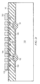
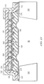
- Figure 1 which includes Figures 1A and 1B , illustrates a MEMS device in accordance with an embodiment of the invention, wherein Figure 1A illustrates a cross sectional view and Figure 1B illustrates a top view;
- Figure 2 which includes Figures 2A-2O , illustrates an embodiment of fabricating the semiconductor device comprising a MEMS sensor in accordance with embodiments of the invention
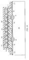
- Figure 3 illustrates an embodiment of a MEMS device in which the membrane layer includes multiple corrugations
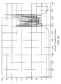
- Figure 4 which includes Figures 4A and 4B , illustrates lateral stress along the membrane layer for two different configurations of the corrugation, wherein Figure 4A illustrates the stress for a corrugation with sharp edges, and wherein Figure 4B illustrates the stress for a corrugation with smooth edges as described herein in various embodiments;
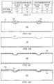
- Figure 5 illustrates a table summarizing the simulation results of Figure 4 ;
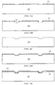
- Figure 6 which includes Figure 6A-6D , illustrates a MEMS device with a membrane layer having negative corrugations during various stages of fabrication, in accordance with an embodiment of the invention
- Figure 7 which includes Figure 7A-7D , illustrates a MEMS device during various stages of processing in accordance with an embodiment in which the membrane layer of the MEMS device is formed over a plurality of substrate protrusions;
- Figure 8 which includes Figures 8A-8C , illustrates an embodiment of the invention of a MEMS device in various stages of processing, wherein a membrane layer of the MEMS device includes positive and negative corrugations;
- Figure 9 which includes Figures 9A-9E , illustrates cross-sectional views of a MEMS device during various stages of fabrication in accordance with another embodiment of the invention.
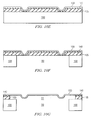
- Figure 10 which includes Figures 10A-10G , illustrates cross-sectional views of a MEMS device during various stages of fabrication in accordance with another embodiment of the invention
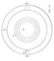
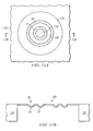
- Figure 11 which includes Figures 11A and 11B , illustrates a MEMS device having a circular membrane in accordance with an embodiment of the invention, wherein Figure 11A illustrates a top view and Figure 11B illustrates a cross-sectional view;
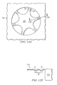
- Figure 12 which includes Figures 12A and 12B , illustrates a MEMS device having a spring supported membrane in accordance with an embodiment of the invention, wherein Figure 12A illustrates a top view and Figure 12B illustrates a cross-sectional view; and
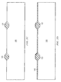
- Figure 13 illustrates a top view of a MEMS device having a spring supported membrane in accordance with an alternative embodiment of the invention.
- MEMS Micro electro-mechanical systems
- a structural embodiment of a MEMS sensor will be described using Figure 1 . Further structural embodiments will be described using Figure 3-5 , 11 . A method of fabricating the MEMS sensor will be described using Figure 2 . Further methods of fabricating the MEMS sensor will be described using Figures 6-10 .
- Figure 1 which includes Figures 1A and 1B , illustrates a MEMS device in accordance with an embodiment of the invention, wherein Figure 1A illustrates a cross sectional view and Figure 1B illustrates a top view.
- the MEMS device comprises a membrane layer 150 disposed over a substrate 100.
- the membrane layer 150 is held over the substrate 100 and supported by a support structure comprising a spacer structure 210 and a protective layer 240.
- the membrane layer 150 comprises corrugations 25 to relieve stress across the membrane layer 150 especially when the membrane layer 150 is under maximum strain (deflection).
- the corrugations 25 comprise smooth edges having no sharp corners. The smooth edges avoid stress concentration within the corrugations 25. Material fracture is a function of crack nucleation and growth, which are a function of the peak stress concentration. Therefore, reducing the peak stress reduces crack nucleation thereby preventing fracture of the membrane layer 150.
- the use of smooth edges thus reduces the failure rate of the membrane layer 150 during operation thereby improving product life time.
- the embodiments of the invention improve mechanical sensitivity of the silicon microphone, which may help to produce microphones with high signal to noise ratio and high sensitivity.
- the MEMS device further comprises a back plate 200.
- a plurality of bumps 195 is disposed on the back surface of the back plate 200.
- Contacts 230 electrically couple to the back plate 200, the membrane layer 150, and the substrate 100.
- the plurality of bumps 195 prevent the membrane layer 150 from sticking to the back plate 200 by minimizing the contact surface area when the membrane layer 150 deflects towards to the back plate 150.
- the MEMS device further includes a central cavity 50 and a gap 55 between the back plate 200 and the membrane layer 150. The central cavity 50 and the gap 55 allow the membrane layer 150 to oscillate.
- the corrugations 25 are formed in a circular shape along the perimeter of the membrane layer 150.
- the circular shape avoids sharp edges along the lateral direction. Therefore, even if the membrane layer 150 is patterned in other shapes (such as rectangular, square shaped), the corrugations 25 may be formed as a circular or elliptical shape. Alternatively, the corrugations 25 may be formed as a square or rectangular shaped but having round edges in regions where two adjacent sides intersect.
- the embodiment illustrated in Figure 1A has positive corrugations (protruding part of the membrane layer 150 faces away from the substrate 100), the embodiments of the present invention also include negative corrugations or mixed corrugations.
- each corrugation of the corrugations 25 has a sidewall and a bottom surface. Both the curvature of transition from sidewall to top surface of the corrugation 25 (having an first radius of curvature R1) and the curvature of the edge of sidewall to bottom surface (having a second radius of curvature R2) of the corrugation 25 have a smooth transition.
- the first and the second radius of curvatures R1 and R2 are about the same value and the first and the second radius of curvatures R1 and R2 are greater than the membrane layer 150, and greater by at least an order of magnitude in one embodiment.
- the second radius of curvature R2 connecting the sidewall and the bottom surface is greater than about 100 nm so that a smooth transition is provided.
- embodiments of the invention are described using back plate 200 and a plurality of bumps 195, in other embodiments these may be not used.
- embodiments of the invention include MEMS applications requiring a membrane layer 150 but with a back plate 200, e.g., pressure sensing with piezoelectric or piezoresistive or optical or else read out.
- embodiments of the invention include multiple back plates, for example, capacitive sensors/actuators where the membrane layer 150 may be sandwiched between two back plates for differential read out or push-pull actuation.
- Figure 2 which includes Figures 2A-2O , illustrates an embodiment of fabricating the semiconductor device comprising a MEMS sensor in accordance with embodiments of the invention.
- FIG. 2A illustrates a masking layer 110 formed over a substrate 100.
- the substrate 100 may be a semiconductor substrate in various embodiments.
- the substrate 100 may be a semiconductor bulk substrate or a semiconductor on insulator substrate in some embodiments.
- Some examples of the substrate 100 include a bulk mono-crystalline silicon substrate (or a layer grown thereon or otherwise formed therein), a layer of ⁇ 110 ⁇ silicon on a ⁇ 100 ⁇ silicon wafer, a layer of a silicon-on-insulator (SOI) wafer, or a layer of a germanium-on-insulator (GeOI) wafer.
- the substrate 100 may include blanket epitaxial layers.
- the substrate 100 may be a silicon wafer, a germanium wafer, or may be a compound semiconductor substrate including indium antimonide, indium arsenide, indium phosphide, gallium nitride, gallium arsenide, gallium antimonide, lead telluride, or combinations thereof.
- the masking layer 110 comprises an insulating layer in various embodiments.
- the masking layer 110 may be a nitride in one embodiment. In another embodiment, the masking layer 110 may be an oxide.
- the masking layer 110 may be formed by thermal oxidation or nitridation, or using vapor deposition processes such as chemical vapor deposition, plasma vapor deposition.
- the masking layer 110 may comprise a hard mask material in one embodiment.
- the masking layer 110 may comprise a nitride material such as silicon nitride.
- the masking layer 110 comprises a pad oxide layer and a silicon nitride layer over the pad oxide layer.
- the masking layer 110 comprises a pad oxide layer, a poly silicon layer over the pad oxide layer, and a silicon nitride layer over the poly silicon layer.
- the masking layer 110 comprises a pad oxide layer, a amorphous silicon layer over the pad oxide layer, and a silicon nitride layer over the amorphous silicon layer.
- the masking layer 110 is patterned for forming regions of local oxide, which as described further below form patterns for the corrugations of the membrane layer.
- the masking layer 110 is patterned, e.g., by depositing a layer of photosensitive material (not shown) such as a photo resist over the masking layer 110.
- the layer of photosensitive material is patterned using a lithography process, e.g., by exposure to light or radiation to transfer a pattern from a lithography mask (not shown) to the layer of photosensitive material, and the photosensitive material is developed.
- the layer of photosensitive material is then used as an etch mask while portions of the masking layer 110 are etched away, leaving the structure shown in Figure 2A .
- oxide regions 120 define the structures for the corrugation grooves in the membrane that is being fabricated.
- Exposed portions of the substrate 100 are oxidized using a thermal oxidation process to form oxide regions 120.
- the masking layer 110 blocks oxidation of the underlying substrate 100. Therefore, the oxidation proceeds locally.
- the masking layer 110 protects other regions (such as other device regions) of the substrate 100 from being oxidized while forming a thick local oxide in exposed portions of the substrate 100.
- the oxidation may be performed using a dry oxidation, wet oxidation, a water ambient, or a mixed ambient.
- the substrate 100 may be exposed to an oxygen-containing substance, a silicon-containing substance, and/or increased temperature to convert a portion of the substrate 100 into an oxide material.
- a surface layer of silicon reacts to form an oxide. Subsequent oxidation progresses by diffusion of oxygen through the oxide layer and reacting at the interface between the growing oxide and the substrate 100.
- a smoothing layer may be deposited over the substrate 100 before forming the masking layer 110.
- the smoothing layer may be formed as a blanket layer or alternatively, over the substrate 100 only in the regions of the MEMS device that is being fabricated.
- the smoothing layer may be a poly silicon layer in one embodiment and may result in smoother corners due to improved stress relaxation during the oxidation process.
- the substrate 100 may be etched using an anisotropic or isotropic etch before exposing to the oxidation process. This may allow tailoring of the lateral profile of the oxide regions 120 formed under the masking layer 110.
- the oxidation process is continued to form oxide regions 120 having a depth of about 1000 nm to about 6000 nm, and having a width of about 1 ⁇ m to about 20 ⁇ m.
- the masking layer 110 is then removed, as illustrated in Figure 2C . Because of the nature of the oxidation process a portion of the oxide regions 120 protrudes above the top surface of the substrate 100. Further, the oxide regions 120 have a smooth interface (silicon/oxide boundary) because of the oxidation process. Oxidation, unlike deposition processes, is a diffusion-reaction process involving high temperatures and relatively slower oxidation rates, which results in an interface having no sharp edges between the substrate 100 and the oxide regions 120. In some embodiments, further smoothing may be performed, for example, by the use of additional anneals such as in an hydrogen atmosphere. The hydrogen anneal may further smooth the oxide regions 120 particularly around the corners and result in a smooth profile as illustrated in Figure 2C .
- a first sacrificial liner 140 is deposited over the substrate 100.
- the first sacrificial liner 140 is an oxide, such as silicon oxide, in one embodiment.
- the first sacrificial liner 140 may be deposited using a vapor deposition process such as chemical vapor deposition, or plasma vapor deposition in various embodiments.
- the first sacrificial liner 140 comprises a thickness of about 100 nm to about 1000 nm.
- a membrane layer 150 is deposited over the first sacrificial liner 140.
- the membrane layer 150 may form an electrode of a capacitor in various embodiments.
- the membrane layer 150 forming the capacitor is part of a capacitive microphone.
- the membrane layer 150 may be formed incorporating the structural features (such as the smooth transitions) described in various embodiments, for example, as described with respect to Figure 1A .
- the membrane layer 150 comprises a poly silicon layer. In an alternative embodiment, the membrane layer 150 comprises a amorphous silicon layer. In alternative embodiments, the membrane layer 150 comprises a conductive layer.
- the membrane layer 150 has a thickness of about 100 nm to about 2000 nm in various embodiments. In one or more embodiments, the membrane layer 150 has a thickness of about 200 nm to about 1000 nm, and about 330 nm in one embodiment.
- the membrane layer 150 and optionally the underlying first sacrificial liner 140 may be patterned.
- the membrane layer 150 is removed from other regions of the substrate 100.
- a first sacrificial material layer 160 is deposited over the membrane layer 150.
- the first sacrificial material layer 160 may comprise an oxide, such as tetra ethyl oxysilane (TEOS).
- TEOS tetra ethyl oxysilane
- the first sacrificial material layer 160 is patterned to form recesses 170.
- the recesses 170 define structures for forming bumps in the back plate as will be described below.
- the lateral geometry of the recesses 170 is chosen such that the recesses 170 for the definition of the bumps are so narrow that the recesses 170 will be almost closed after a subsequent layer deposition.
- the recesses 170 may comprise a width of about 1000 nm if a subsequent layer of 600 nm is deposited.
- the lateral dimension of the recesses 170 is approximately in the range of the thickness of the subsequent layer to be disposed.
- a second sacrificial liner 180 is deposited over the first sacrificial material layer 160.
- the second sacrificial liner 180 may be the same material as the the first sacrificial material layer 160.
- the second sacrificial liner 180 may be a etch stop liner material in one embodiment.
- the thickness of the second sacrificial liner 180 is chosen so as to approximately fill the recesses 170. Consequently, bump holes 185 having a sharp triangle-like shape are formed after depositing the second sacrificial liner 180.
- the bump liner 190 is deposited forming a plurality of bumps 195.
- the bump liner 190 comprises a material having a different etch selectivity than the first sacrificial material layer 160.
- the bump liner 190 may be an etch stop liner material in one embodiment. Because of the sharp cavities of the bump holes 185, the bump liner 190 includes sharp needle like shape, which minimizes the contact surface area between the membrane layer 150 and the plurality of bumps 195 if the membrane layer 150 contacts the plurality of bumps 195 during device operation.
- a back plate 200 is deposited over the bump liner 190 and patterned.
- the exposed bump liner 190 may also be patterned.
- the back plate 200 forms a portion of a capacitor, for example, a portion of a capacitive microphone.
- the back plate 200 comprises a poly silicon material in one embodiment.
- contacts 230 and spacer structures 210 are formed.
- the first sacrificial material layer 160 may be removed from an outside region leaving spacer structures 210 for supporting the MEMS device region.
- a protective liner 220 is deposited covering the back plate 200.
- Contacts 230 are formed to couple the back plate 200 and the membrane layer 150. The contacts 230 are formed after masking and patterning the protective liner 220.
- the front side is protected by forming a protective layer 240.
- the protective layer 240 protects the front side during the subsequent back side processing.
- the protective layer 240 may comprise silicon nitride or silicon oxide.
- Back side processing continues from Figure 2L to form a cavity 50.
- the wafer is reversed to expose the back side.
- a resist is deposited on the exposed back side and patterned (not shown) and a portion of the substrate 100 in the MEMS device region is exposed.
- the exposed substrate 100 is etched until the first sacrificial liner 140 and the oxide regions 120 are exposed.
- the substrate 100 may be etched using a Bosch Process, or by depositing a hard mask layer and etching the substrate 100 using a vertical reactive ion etch. In one embodiment, only a resist mask is used. If the resist budget is not sufficient, the hard mask and vertical reactive ion etch may be used to achieve a smooth sidewall. However, this integration scheme requires the removal of remaining hard mask residues. Hence, in some embodiments, a Bosch process may be used without additional hard mask.
- a isotropic plasma etch step and passivation layer deposition step are alternated.
- the etching/deposition steps are repeated many times during the Bosch process.
- the plasma etch is configured to etch vertically, e.g., using Sulfur hexafluoride [SF6] in the plasma.
- the passivation layer is deposited, for example, using octa-fluoro-cyclobutane as a source gas. Each individual step may be turned on for a few seconds or less.
- the passivation layer protects the substrate 100 and prevents further etching.
- the directional ions that bombard the substrate remove the passivation layer at the bottom of the trench (but not along the sides) and etching continues.
- the Bosch process is stopped when the first sacrificial liner 140 and the oxide regions 120 are exposed.
- the Bosch process produces sidewalls that are scalloped.
- the first sacrificial liner 140 and the oxide regions 120 are removed, for example, using a wet etch chemistry.
- the wet etch stops after the membrane layer 150 is exposed.
- the front side is patterned to open the MEMS device area while protecting the remaining regions, for example, the contacts 230.
- a resist 250 is deposited over the front side and patterned as illustrated.
- the resist 250 may comprise a silicon nitride material in one embodiment, and may comprise a hard mask in one embodiment.
- the MEMS device region may be exposed to a wet etch process that may be able to efficiently remove a particular type of material.
- the first sacrificial material layer 160 and the second sacrificial liner 180 are removed, e.g., using a wet etching process.
- the protective layer 240 is removed.
- the protective layer 240 may be etched, using an anisotropic etch process, leaving a support spacer.
- the first sacrificial material layer 160 and the second sacrificial liner 180 may be removed from the front side in one embodiment after removing the protective layer 240.
- the first sacrificial material layer 160, the second sacrificial liner 180, the oxide regions 120, and the first sacrificial liner 140 may be removed during the same step.
- the corrugations 25 in the membrane 150 are positive, i.e., facing away from the substrate 100.
- Figure 3 illustrates an embodiment of a MEMS device in which the membrane layer includes multiple corrugations.
- the number of corrugations may be chosen to optimize the stress in the membrane layer 150. Therefore, embodiments of the invention may be fabricated using multiple oxide regions 120, which results in increasing the number of corrugations.
- Figure 3 illustrates two corrugations 25, and in various more number of corrugations may be formed.
- Figure 4 which includes Figures 4A and 4B , illustrates lateral stress along the membrane layer for two different configurations of the corrugation, wherein Figure 4A illustrates the stress for a corrugation with sharp edges, and wherein Figure 4B illustrates the stress for a corrugation with smooth edges as described herein in various embodiments.
- Figure 4 illustrates simulation results obtained after Finite Element Modeling Simulations (FEM) of the two different types of corrugation structures.
- FEM Finite Element Modeling Simulations
- the origin of the plot in Figures 4A and 4B is the center of the membrane layer such that the x-axis is along the radius of the membrane layer towards the support structures (see, e.g., Figure 1 ).
- FEM Finite Element Modeling Simulations
- the stress is flat and increases dramatically in the corrugated regions. This may result in breaking of the membrane, e.g., due to crack nucleation and growth when a critical stress is reached.
- the peak stress is a significant metric as crack nucleation begins from such regions.
- the use of smooth edges as described in various embodiments reduces the peak stress within the corrugation regions.
- Figure 4 illustrates the lateral component of the stress
- the inventors find other quantitative measures such as Von Mises stress, which suggests the onset of plastic deformation, also show a similar difference between corrugations having sharp edges and corrugations having smooth edges as described in various embodiments of the present invention.
- Figure 5 illustrates a table summarizing the simulation results of Figure 4 .
- the table shows the value of the peak stress when pressure is applied from the top and bottom of the membrane layer, which relates to +/- vertical displacement of the membrane layer.
- the peak stress values drop significantly when the sharp edge is replaced with a smooth edge (compare first row, which is for a sharp edge, to the second row, which is for the smooth edge).
- Figure 6 which includes Figure 6A-6D , illustrates a MEMS device with a membrane layer having negative corrugations during various stages of fabrication, in accordance with an embodiment of the invention.
- the oxide regions 120 are formed as described above in prior embodiments (see e.g., Figure 2B ). After forming the oxide regions 120 having smoothed edges as described in various embodiments, the masking layer 110 and the oxide regions 120 are removed. Thus a plurality of trenches 125 are formed within the substrate 100 as illustrated in Figure 6B .
- a first sacrificial liner 140 is formed.
- the first sacrificial liner 140 may comprise a silicon oxide material in one embodiment.
- the first sacrificial liner 140 lines the plurality of trenches 125.
- the thickness of the first sacrificial liner 140 is much smaller than the dimensions of the plurality of trenches 125 so that the first sacrificial liner 140 does not significantly fill the plurality of trenches 125.
- a membrane layer 150 is formed over the first sacrificial liner 140. Subsequent processing follows as described in the embodiment following Figures 2F-2O . Because the first sacrificial liner 140 and the membrane layer 150 are formed within the plurality of trenches 125, the resulting corrugations in the membrane 150 are negative corrugations 225 (relative to the positive corrugations of Figure 2 ) facing towards the substrate 100.
- Figure 7 which includes Figure 7A-7D , illustrates a MEMS device during various stages of processing in accordance with an embodiment in which the membrane layer of the MEMS device is formed over a plurality of substrate protrusions.
- a masking layer 110 is deposited as in prior embodiments. However, the masking layer 110 is patterned negatively relative to the embodiment of Figure 2 . Unlike Figure 2 , the masking layer 110 is not removed from regions in which corrugations are to be formed. Rather, the masking layer 110 is removed from regions in which corrugations are not to be formed.
- the exposed substrate 100 is next oxidized locally as described above with respect to Figure 2 forming an oxide/substrate profile with smooth edges ( Figure 7B ). Because of the volume expansion of oxide relative to silicon, the top surface of the oxide regions 120 rises above the remaining substrate 100. For the same reason, the lower surface of the oxide regions 120 is below the top surface of the remaining substrate 100.
- the masking layer 110 and the oxide regions 120 are removed leaving a plurality of substrate protrusions 710.
- a first sacrificial liner 140 and a membrane layer 150 are formed. Subsequent processing follows as described in the embodiment following Figures 2F-2O . Because the first sacrificial liner 140 and the membrane layer 150 are formed over the plurality of substrate protrusions, the resulting corrugations in the membrane 150 are corrugations 25 with positive curvature (facing away from the substrate 100).
- Figure 8 which includes Figures 8A-8C , illustrates an embodiment of the invention of a MEMS device in various stages of processing, wherein a membrane layer of the MEMS device includes positive and negative corrugations.
- oxide regions 120 are formed as described with respect to Figure 2B . Similar to the embodiment of Figure 6 , the oxide regions 120 are removed. However, unlike the embodiment of Figure 6 , only some of the oxide regions 120 are removed in this embodiment ( Figure 8B ). For example, a region of the MEMS device is covered, for example, by forming an etch mask, and some of the oxide regions 120 are removed leaving a plurality of trenches 125.
- the plurality of trenches 125 and the remaining oxide regions 120 are covered with a first sacrificial liner 140 and a membrane layer 150 as described in prior embodiments. Subsequent processing following the embodiments discussed above with respect to Figure 2 , e.g., Figures 2F-2O .
- the membrane layer 150 having both positive and negative corrugations may be formed.
- Figure 9 which includes Figures 9A-9E , illustrates cross-sectional views of a MEMS device during various stages of fabrication in accordance with another embodiment of the invention.
- this embodiment forms corrugations having smooth edges by using an etch process.
- a masking layer 110 is formed over a substrate 100 as in other embodiments (e.g., Figure 2A ).
- a plurality of trenches 125 is formed without oxidization. Rather, in this embodiment, an etching technique is used.
- an isotropic etching is used to form the plurality of trenches 125.
- the depth of the plurality of trenches 125 is adjusted by the etching time in one embodiment. Therefore, this process may be susceptible to more variations. Accordingly in one embodiment, the surface of the substrate 100 may be doped to reduce the etch rate, which may help to reduce variations. Similarly, the etching chemistry may be selected to reduce variations and improve control of the process as known to one skilled in the art.
- the masking layer 110 is removed as illustrated in Figure 9C .
- a first sacrificial liner 140 is formed over the substrate 100 and the plurality of trenches 125.
- a membrane layer 150 is formed over the first sacrificial liner 140 as described in prior embodiments ( Figure 9E ). Subsequent processing follows as described in the embodiment following Figures 2F-2O .
- Figure 10 which includes Figures 10A-10G , illustrates cross-sectional views of a MEMS device during various stages of fabrication in accordance with another embodiment of the invention.
- this embodiment forms corrugations using an additional insulating layer.
- a masking layer 110 is formed as in other embodiments (e.g., Figure 2A ). However, unlike the prior embodiments, the masking layer 110 is formed over an additional insulating layer 105.
- the additional insulating layer 105 may be deposited over the substrate 100.
- the additional insulating layer 105 may comprise an oxide in one embodiment, whereas in some embodiments, the additional insulating layer 105 may comprise other materials such as nitrides.
- an isotropic etching is used to form the plurality of trenches 125.
- the depth of the plurality of trenches 125 is adjusted by the thickness of the additional insulating layer 105. Therefore, this process may be susceptible to less process variation relative to the embodiment of Figure 9 .
- the masking layer 110 is removed as illustrated in Figure 10C .
- a first sacrificial liner 140 is formed over the substrate 100 and the plurality of trenches 125.
- a membrane layer 150 is formed over the first sacrificial liner 140 as described in prior embodiments ( Figure 10E ).
- Subsequent processing follows as described in the embodiment following Figures 2F-2O .
- the cavity 50 is formed from the back side of the substrate 100.
- an additional etch may be performed to remove the additional insulating layer 105 and the first sacrificial liner 140. If the additional insulating layer 105 and the first sacrificial liner 140 comprise a same material, a single etch may be used to remove both the layers.
- Figure 11 which includes Figures 11A and 11B , illustrates a MEMS device having a circular membrane in accordance with an embodiment of the invention, wherein Figure 11A illustrates a top view and Figure 11B illustrates a cross-sectional view.
- the membrane layer 150 is formed over the substrate 100 and includes corrugations 25.
- the corrugations 25 comprise a first corrugation 26 separated from a second corrugation 27 by a flat region of the membrane layer 150.
- Figure 12 which includes Figures 12A and 12B , illustrates a MEMS device having a spring supported membrane in accordance with an embodiment of the invention, wherein Figure 12A illustrates a top view and Figure 12B illustrates a cross-sectional view.
- the membrane layer 150 is formed over the substrate 100 and includes corrugations 25. However, in this embodiment, a central portion of the membrane layer 150 is supported by a plurality of support structures 30.
- the plurality of support structures 30 comprise corrugations 25 as described in various embodiments.
- Figure 13 illustrates a top view of a MEMS device having a spring supported membrane in accordance with an alternative embodiment of the invention.
- a plurality of support structures 30 support the membrane layer 150 to the substrate 100.
- the plurality of support structures 30 comprises a first support 151, a second support 152, a third support 153, and a fourth support 154.
- Each support of the plurality of support structures 30 is oriented orthogonally to an adjacent support in one embodiment, as illustrated in Figure 13 .
- Each support of the plurality of support structures 30 comprise corrugations 25 as described in various embodiments.
- a particular embodiment of the invention provides a method of manufacturing a semiconductor device, the method comprising:
- forming the membrane layer comprises depositing a poly silicon layer, wherein the back plate layer comprises silicon.
- a third further development of the first further development further comprises:
- a fourth further development of the third further development further comprises:
- a fifth further development of the fourth further development comprises:
- a seventh further development of the particular embodiment further comprises depositing a liner over the local oxide regions before forming the membrane layer.
Landscapes
- Engineering & Computer Science (AREA)
- Physics & Mathematics (AREA)
- Acoustics & Sound (AREA)
- Signal Processing (AREA)
- Microelectronics & Electronic Packaging (AREA)
- Manufacturing & Machinery (AREA)
- Computer Hardware Design (AREA)
- Mechanical Engineering (AREA)
- Multimedia (AREA)
- Micromachines (AREA)
- Pressure Sensors (AREA)
Abstract
Description
- The present invention relates generally to micro-electromechanical systems devices, and more particularly to semiconductor devices and methods of fabrications thereof.
- Small electromechanical components can be manufactured using micro-electromechanical systems (MEMS) technology using microelectronics manufacturing processes. MEMS devices include thin membranes and beams, which function as mechanical and/or electrical components.
- Silicon microphone are a type of MEMS device in which the MEMS structure or a membrane actuates with acoustic signals. However, the sensitivity of the membrane, and therefore, the MEMS device varies with stress in the membrane. For example, tensile stress severely decreases the mechanical compliance of the microphone.
- Stress may be residual, which is formed during the fabrication, or may build up during operation. Therefore, MEMS devices and methods which minimize film stress are needed.
- These and other problems are generally solved or circumvented, and technical advantages are generally achieved, by illustrative embodiments of the present invention.
- In accordance with an embodiment of the invention, a method of manufacturing a semiconductor device comprises oxidizing a substrate to form local oxide regions extending above a top surface of the substrate, and forming a membrane layer over the local oxide regions and the top surface of the substrate. The method further comprises removing a portion of the substrate under the membrane layer, and removing the local oxide regions under the membrane layer.
- In accordance with an embodiment of the invention, method of manufacturing a semiconductor device comprises forming a plurality of features in a substrate, and forming a membrane layer over the substrate comprising the plurality of features. The method further comprises removing a portion of the substrate under the membrane layer.
- In accordance with an embodiment of the invention, a semiconductor device comprises a membrane layer comprising a plurality of corrugations disposed over a substrate. Each corrugation of the plurality of corrugations have a sidewall and a bottom surface. A radius of curvature of an edge connecting the sidewall and the bottom surface is greater than a thickness of the membrane layer. A radius of curvature of an edge connecting the sidewall and the top surface is greater than the thickness of the membrane layer.
- The foregoing has outlined rather broadly the features of an embodiment of the present invention in order that the detailed description of the invention that follows may be better understood. Additional features and advantages of embodiments of the invention will be described hereinafter, which form the subject of the claims of the invention. It should be appreciated by those skilled in the art that the conception and specific embodiments disclosed may be readily utilized as a basis for modifying or designing other structures or processes for carrying out the same purposes of the present invention. It should also be realized by those skilled in the art that such equivalent constructions do not depart from the spirit and scope of the invention as set forth in the appended claims.
- For a more complete understanding of the present invention, and the advantages thereof, reference is now made to the following descriptions taken in conjunction with the accompanying drawing, in which:
-
Figure 1 , which includesFigures 1A and1B , illustrates a MEMS device in accordance with an embodiment of the invention, whereinFigure 1A illustrates a cross sectional view andFigure 1B illustrates a top view; -
Figure 2 , which includesFigures 2A-2O , illustrates an embodiment of fabricating the semiconductor device comprising a MEMS sensor in accordance with embodiments of the invention; -
Figure 3 illustrates an embodiment of a MEMS device in which the membrane layer includes multiple corrugations; -
Figure 4 , which includesFigures 4A and4B , illustrates lateral stress along the membrane layer for two different configurations of the corrugation, whereinFigure 4A illustrates the stress for a corrugation with sharp edges, and whereinFigure 4B illustrates the stress for a corrugation with smooth edges as described herein in various embodiments; -
Figure 5 illustrates a table summarizing the simulation results ofFigure 4 ; -
Figure 6 , which includesFigure 6A-6D , illustrates a MEMS device with a membrane layer having negative corrugations during various stages of fabrication, in accordance with an embodiment of the invention; -
Figure 7 , which includesFigure 7A-7D , illustrates a MEMS device during various stages of processing in accordance with an embodiment in which the membrane layer of the MEMS device is formed over a plurality of substrate protrusions; -
Figure 8 , which includesFigures 8A-8C , illustrates an embodiment of the invention of a MEMS device in various stages of processing, wherein a membrane layer of the MEMS device includes positive and negative corrugations; -
Figure 9 , which includesFigures 9A-9E , illustrates cross-sectional views of a MEMS device during various stages of fabrication in accordance with another embodiment of the invention; -
Figure 10 , which includesFigures 10A-10G , illustrates cross-sectional views of a MEMS device during various stages of fabrication in accordance with another embodiment of the invention; -
Figure 11 , which includesFigures 11A and 11B , illustrates a MEMS device having a circular membrane in accordance with an embodiment of the invention, whereinFigure 11A illustrates a top view andFigure 11B illustrates a cross-sectional view; -
Figure 12 , which includesFigures 12A and 12B , illustrates a MEMS device having a spring supported membrane in accordance with an embodiment of the invention, whereinFigure 12A illustrates a top view andFigure 12B illustrates a cross-sectional view; and -
Figure 13 illustrates a top view of a MEMS device having a spring supported membrane in accordance with an alternative embodiment of the invention. - Corresponding numerals and symbols in the different figures generally refer to corresponding parts unless otherwise indicated. The figures are drawn to clearly illustrate the relevant aspects of the embodiments and are not necessarily drawn to scale.
- The making and using of various embodiments are discussed in detail below. It should be appreciated, however, that the present invention provides many applicable inventive concepts that can be embodied in a wide variety of specific contexts. The specific embodiments discussed are merely illustrative of specific ways to make and use the invention, and do not limit the scope of the invention.
- The present invention will be described with respect to various embodiments in a specific context, namely a Micro electro-mechanical systems (MEMS) sensor. The invention may also be applied, however, to other types of semiconductor devices.
- A structural embodiment of a MEMS sensor will be described using
Figure 1 . Further structural embodiments will be described usingFigure 3-5 ,11 . A method of fabricating the MEMS sensor will be described usingFigure 2 . Further methods of fabricating the MEMS sensor will be described usingFigures 6-10 . -
Figure 1 , which includesFigures 1A and1B , illustrates a MEMS device in accordance with an embodiment of the invention, whereinFigure 1A illustrates a cross sectional view andFigure 1B illustrates a top view. - Referring to
Figure 1A , the MEMS device comprises amembrane layer 150 disposed over asubstrate 100. Themembrane layer 150 is held over thesubstrate 100 and supported by a support structure comprising aspacer structure 210 and aprotective layer 240. Themembrane layer 150 comprisescorrugations 25 to relieve stress across themembrane layer 150 especially when themembrane layer 150 is under maximum strain (deflection). Further, as further explained in various embodiments, thecorrugations 25 comprise smooth edges having no sharp corners. The smooth edges avoid stress concentration within thecorrugations 25. Material fracture is a function of crack nucleation and growth, which are a function of the peak stress concentration. Therefore, reducing the peak stress reduces crack nucleation thereby preventing fracture of themembrane layer 150. The use of smooth edges thus reduces the failure rate of themembrane layer 150 during operation thereby improving product life time. Alternatively, the embodiments of the invention improve mechanical sensitivity of the silicon microphone, which may help to produce microphones with high signal to noise ratio and high sensitivity. - The MEMS device further comprises a
back plate 200. A plurality ofbumps 195 is disposed on the back surface of theback plate 200. Contacts 230 electrically couple to theback plate 200, themembrane layer 150, and thesubstrate 100. The plurality ofbumps 195 prevent themembrane layer 150 from sticking to theback plate 200 by minimizing the contact surface area when themembrane layer 150 deflects towards to theback plate 150. The MEMS device further includes acentral cavity 50 and agap 55 between theback plate 200 and themembrane layer 150. Thecentral cavity 50 and thegap 55 allow themembrane layer 150 to oscillate. - As illustrated in
Figure 1B , thecorrugations 25 are formed in a circular shape along the perimeter of themembrane layer 150. The circular shape avoids sharp edges along the lateral direction. Therefore, even if themembrane layer 150 is patterned in other shapes (such as rectangular, square shaped), thecorrugations 25 may be formed as a circular or elliptical shape. Alternatively, thecorrugations 25 may be formed as a square or rectangular shaped but having round edges in regions where two adjacent sides intersect. - Although, the embodiment illustrated in
Figure 1A , has positive corrugations (protruding part of themembrane layer 150 faces away from the substrate 100), the embodiments of the present invention also include negative corrugations or mixed corrugations. - As illustrated in
Figure 1A , each corrugation of thecorrugations 25 has a sidewall and a bottom surface. Both the curvature of transition from sidewall to top surface of the corrugation 25 (having an first radius of curvature R1) and the curvature of the edge of sidewall to bottom surface (having a second radius of curvature R2) of thecorrugation 25 have a smooth transition. In or more embodiments, the first and the second radius of curvatures R1 and R2 are about the same value and the first and the second radius of curvatures R1 and R2 are greater than themembrane layer 150, and greater by at least an order of magnitude in one embodiment. In one embodiment, the second radius of curvature R2 connecting the sidewall and the bottom surface is greater than about 100 nm so that a smooth transition is provided. - While embodiments of the invention are described using
back plate 200 and a plurality ofbumps 195, in other embodiments these may be not used. For example, embodiments of the invention include MEMS applications requiring amembrane layer 150 but with aback plate 200, e.g., pressure sensing with piezoelectric or piezoresistive or optical or else read out. Similarly embodiments of the invention include multiple back plates, for example, capacitive sensors/actuators where themembrane layer 150 may be sandwiched between two back plates for differential read out or push-pull actuation. -
Figure 2 , which includesFigures 2A-2O , illustrates an embodiment of fabricating the semiconductor device comprising a MEMS sensor in accordance with embodiments of the invention. -
Figure 2A illustrates amasking layer 110 formed over asubstrate 100. Thesubstrate 100 may be a semiconductor substrate in various embodiments. Thesubstrate 100 may be a semiconductor bulk substrate or a semiconductor on insulator substrate in some embodiments. Some examples of thesubstrate 100 include a bulk mono-crystalline silicon substrate (or a layer grown thereon or otherwise formed therein), a layer of {110} silicon on a {100} silicon wafer, a layer of a silicon-on-insulator (SOI) wafer, or a layer of a germanium-on-insulator (GeOI) wafer. In various embodiments, thesubstrate 100 may include blanket epitaxial layers. In various embodiments, thesubstrate 100 may be a silicon wafer, a germanium wafer, or may be a compound semiconductor substrate including indium antimonide, indium arsenide, indium phosphide, gallium nitride, gallium arsenide, gallium antimonide, lead telluride, or combinations thereof. - The
masking layer 110 comprises an insulating layer in various embodiments. Themasking layer 110 may be a nitride in one embodiment. In another embodiment, themasking layer 110 may be an oxide. Themasking layer 110 may be formed by thermal oxidation or nitridation, or using vapor deposition processes such as chemical vapor deposition, plasma vapor deposition. - The
masking layer 110 may comprise a hard mask material in one embodiment. In various embodiments, themasking layer 110 may comprise a nitride material such as silicon nitride. In one or more embodiments, themasking layer 110 comprises a pad oxide layer and a silicon nitride layer over the pad oxide layer. In an alternative embodiment, themasking layer 110 comprises a pad oxide layer, a poly silicon layer over the pad oxide layer, and a silicon nitride layer over the poly silicon layer. In another alternative embodiment, themasking layer 110 comprises a pad oxide layer, a amorphous silicon layer over the pad oxide layer, and a silicon nitride layer over the amorphous silicon layer. - The
masking layer 110 is patterned for forming regions of local oxide, which as described further below form patterns for the corrugations of the membrane layer. Themasking layer 110 is patterned, e.g., by depositing a layer of photosensitive material (not shown) such as a photo resist over themasking layer 110. The layer of photosensitive material is patterned using a lithography process, e.g., by exposure to light or radiation to transfer a pattern from a lithography mask (not shown) to the layer of photosensitive material, and the photosensitive material is developed. The layer of photosensitive material is then used as an etch mask while portions of themasking layer 110 are etched away, leaving the structure shown inFigure 2A . - As next illustrated in
Figure 2B , local oxidation is performed to formoxide regions 120. As will be described further below, theoxide regions 120 define the structures for the corrugation grooves in the membrane that is being fabricated. Exposed portions of thesubstrate 100 are oxidized using a thermal oxidation process to formoxide regions 120. Themasking layer 110 blocks oxidation of theunderlying substrate 100. Therefore, the oxidation proceeds locally. In one or more embodiments, themasking layer 110 protects other regions (such as other device regions) of thesubstrate 100 from being oxidized while forming a thick local oxide in exposed portions of thesubstrate 100. - In various embodiments, the oxidation may be performed using a dry oxidation, wet oxidation, a water ambient, or a mixed ambient. For example, the
substrate 100 may be exposed to an oxygen-containing substance, a silicon-containing substance, and/or increased temperature to convert a portion of thesubstrate 100 into an oxide material. - During the oxidation process, a surface layer of silicon reacts to form an oxide. Subsequent oxidation progresses by diffusion of oxygen through the oxide layer and reacting at the interface between the growing oxide and the
substrate 100. - In an alternative embodiment, a smoothing layer may be deposited over the
substrate 100 before forming themasking layer 110. The smoothing layer may be formed as a blanket layer or alternatively, over thesubstrate 100 only in the regions of the MEMS device that is being fabricated. The smoothing layer may be a poly silicon layer in one embodiment and may result in smoother corners due to improved stress relaxation during the oxidation process. - Similarly, in an alternative embodiment, the
substrate 100 may be etched using an anisotropic or isotropic etch before exposing to the oxidation process. This may allow tailoring of the lateral profile of theoxide regions 120 formed under themasking layer 110. - In various embodiments, the oxidation process is continued to form
oxide regions 120 having a depth of about 1000 nm to about 6000 nm, and having a width of about 1µm to about 20µm. - The
masking layer 110 is then removed, as illustrated inFigure 2C . Because of the nature of the oxidation process a portion of theoxide regions 120 protrudes above the top surface of thesubstrate 100. Further, theoxide regions 120 have a smooth interface (silicon/oxide boundary) because of the oxidation process. Oxidation, unlike deposition processes, is a diffusion-reaction process involving high temperatures and relatively slower oxidation rates, which results in an interface having no sharp edges between thesubstrate 100 and theoxide regions 120. In some embodiments, further smoothing may be performed, for example, by the use of additional anneals such as in an hydrogen atmosphere. The hydrogen anneal may further smooth theoxide regions 120 particularly around the corners and result in a smooth profile as illustrated inFigure 2C . - Referring next to
Figure 2D , a firstsacrificial liner 140 is deposited over thesubstrate 100. The firstsacrificial liner 140 is an oxide, such as silicon oxide, in one embodiment. The firstsacrificial liner 140 may be deposited using a vapor deposition process such as chemical vapor deposition, or plasma vapor deposition in various embodiments. The firstsacrificial liner 140 comprises a thickness of about 100 nm to about 1000 nm. - Next, as illustrated in
Figure 2E , amembrane layer 150 is deposited over the firstsacrificial liner 140. Themembrane layer 150 may form an electrode of a capacitor in various embodiments. In one embodiment, themembrane layer 150 forming the capacitor is part of a capacitive microphone. In various embodiment, themembrane layer 150 may be formed incorporating the structural features (such as the smooth transitions) described in various embodiments, for example, as described with respect toFigure 1A . - In one embodiment, the
membrane layer 150 comprises a poly silicon layer. In an alternative embodiment, themembrane layer 150 comprises a amorphous silicon layer. In alternative embodiments, themembrane layer 150 comprises a conductive layer. Themembrane layer 150 has a thickness of about 100 nm to about 2000 nm in various embodiments. In one or more embodiments, themembrane layer 150 has a thickness of about 200 nm to about 1000 nm, and about 330 nm in one embodiment. - As illustrated in
Figure 2E , themembrane layer 150 and optionally the underlying firstsacrificial liner 140 may be patterned. Themembrane layer 150 is removed from other regions of thesubstrate 100. - Referring next to
Figure 2F , a firstsacrificial material layer 160 is deposited over themembrane layer 150. In one or more embodiments, the firstsacrificial material layer 160 may comprise an oxide, such as tetra ethyl oxysilane (TEOS). The firstsacrificial material layer 160 is patterned to form recesses 170. Therecesses 170 define structures for forming bumps in the back plate as will be described below. - In various embodiments, the lateral geometry of the
recesses 170 is chosen such that therecesses 170 for the definition of the bumps are so narrow that therecesses 170 will be almost closed after a subsequent layer deposition. For example, therecesses 170 may comprise a width of about 1000 nm if a subsequent layer of 600 nm is deposited. In other words, in various embodiments, the lateral dimension of therecesses 170 is approximately in the range of the thickness of the subsequent layer to be disposed. - Referring to
Figure 2G , a secondsacrificial liner 180 is deposited over the firstsacrificial material layer 160. The secondsacrificial liner 180 may be the same material as the the firstsacrificial material layer 160. The secondsacrificial liner 180 may be a etch stop liner material in one embodiment. As described above, the thickness of the secondsacrificial liner 180 is chosen so as to approximately fill therecesses 170. Consequently, bumpholes 185 having a sharp triangle-like shape are formed after depositing the secondsacrificial liner 180. - As next illustrated in
Figure 2H , thebump liner 190 is deposited forming a plurality ofbumps 195. Thebump liner 190 comprises a material having a different etch selectivity than the firstsacrificial material layer 160. Thebump liner 190 may be an etch stop liner material in one embodiment. Because of the sharp cavities of the bump holes 185, thebump liner 190 includes sharp needle like shape, which minimizes the contact surface area between themembrane layer 150 and the plurality ofbumps 195 if themembrane layer 150 contacts the plurality ofbumps 195 during device operation. - Referring next to
Figure 2I , aback plate 200 is deposited over thebump liner 190 and patterned. The exposedbump liner 190 may also be patterned. In various embodiments, theback plate 200 forms a portion of a capacitor, for example, a portion of a capacitive microphone. Theback plate 200 comprises a poly silicon material in one embodiment. - Referring next to
Figure 2J ,contacts 230 andspacer structures 210 are formed. The firstsacrificial material layer 160 may be removed from an outside region leavingspacer structures 210 for supporting the MEMS device region. Aprotective liner 220 is deposited covering theback plate 200.Contacts 230 are formed to couple theback plate 200 and themembrane layer 150. Thecontacts 230 are formed after masking and patterning theprotective liner 220. - Referring to
Figure 2K , the front side is protected by forming aprotective layer 240. Theprotective layer 240 protects the front side during the subsequent back side processing. In various embodiments, theprotective layer 240 may comprise silicon nitride or silicon oxide. - Back side processing continues from
Figure 2L to form acavity 50. The wafer is reversed to expose the back side. Next a resist is deposited on the exposed back side and patterned (not shown) and a portion of thesubstrate 100 in the MEMS device region is exposed. The exposedsubstrate 100 is etched until the firstsacrificial liner 140 and theoxide regions 120 are exposed. - In various embodiments, the
substrate 100 may be etched using a Bosch Process, or by depositing a hard mask layer and etching thesubstrate 100 using a vertical reactive ion etch. In one embodiment, only a resist mask is used. If the resist budget is not sufficient, the hard mask and vertical reactive ion etch may be used to achieve a smooth sidewall. However, this integration scheme requires the removal of remaining hard mask residues. Hence, in some embodiments, a Bosch process may be used without additional hard mask. - In the Bosch process, a isotropic plasma etch step and passivation layer deposition step are alternated. The etching/deposition steps are repeated many times during the Bosch process. The plasma etch is configured to etch vertically, e.g., using Sulfur hexafluoride [SF6] in the plasma. The passivation layer is deposited, for example, using octa-fluoro-cyclobutane as a source gas. Each individual step may be turned on for a few seconds or less. The passivation layer protects the
substrate 100 and prevents further etching. However, during the plasma etching phase, the directional ions that bombard the substrate remove the passivation layer at the bottom of the trench (but not along the sides) and etching continues. The Bosch process is stopped when the firstsacrificial liner 140 and theoxide regions 120 are exposed. The Bosch process produces sidewalls that are scalloped. - Referring next to
Figure 2M , the firstsacrificial liner 140 and theoxide regions 120 are removed, for example, using a wet etch chemistry. The wet etch stops after themembrane layer 150 is exposed. - Referring to
Figure 2N , the front side is patterned to open the MEMS device area while protecting the remaining regions, for example, thecontacts 230. A resist 250 is deposited over the front side and patterned as illustrated. The resist 250 may comprise a silicon nitride material in one embodiment, and may comprise a hard mask in one embodiment. Thus, the MEMS device region may be exposed to a wet etch process that may be able to efficiently remove a particular type of material. - As next illustrated in
Figure 2O , the firstsacrificial material layer 160 and the secondsacrificial liner 180 are removed, e.g., using a wet etching process. Theprotective layer 240 is removed. In one or more embodiments, theprotective layer 240 may be etched, using an anisotropic etch process, leaving a support spacer. The firstsacrificial material layer 160 and the secondsacrificial liner 180 may be removed from the front side in one embodiment after removing theprotective layer 240. - In some embodiments, the first
sacrificial material layer 160, the secondsacrificial liner 180, theoxide regions 120, and the firstsacrificial liner 140 may be removed during the same step. - Because the first
sacrificial liner 140 and themembrane layer 150 are formed over theoxide regions 120, thecorrugations 25 in themembrane 150 are positive, i.e., facing away from thesubstrate 100. -
Figure 3 illustrates an embodiment of a MEMS device in which the membrane layer includes multiple corrugations. In various embodiments, the number of corrugations may be chosen to optimize the stress in themembrane layer 150. Therefore, embodiments of the invention may be fabricated usingmultiple oxide regions 120, which results in increasing the number of corrugations.Figure 3 illustrates twocorrugations 25, and in various more number of corrugations may be formed. -
Figure 4 , which includesFigures 4A and4B , illustrates lateral stress along the membrane layer for two different configurations of the corrugation, whereinFigure 4A illustrates the stress for a corrugation with sharp edges, and whereinFigure 4B illustrates the stress for a corrugation with smooth edges as described herein in various embodiments. -
Figure 4 illustrates simulation results obtained after Finite Element Modeling Simulations (FEM) of the two different types of corrugation structures. Referring toFigure 4 , the origin of the plot inFigures 4A and4B is the center of the membrane layer such that the x-axis is along the radius of the membrane layer towards the support structures (see, e.g.,Figure 1 ). These simulations are performed for eight corrugation rings on a membrane of 0.9 mm diameter, however, the general idea may be extended to any number of rings and membrane sizes. - As illustrated in
Figure 4A , the stress is flat and increases dramatically in the corrugated regions. This may result in breaking of the membrane, e.g., due to crack nucleation and growth when a critical stress is reached. For crack propagation, the peak stress is a significant metric as crack nucleation begins from such regions. However, as illustrated inFigure 4B , the use of smooth edges as described in various embodiments, reduces the peak stress within the corrugation regions. - While
Figure 4 illustrates the lateral component of the stress, the inventors find other quantitative measures such as Von Mises stress, which suggests the onset of plastic deformation, also show a similar difference between corrugations having sharp edges and corrugations having smooth edges as described in various embodiments of the present invention. -
Figure 5 illustrates a table summarizing the simulation results ofFigure 4 . The table shows the value of the peak stress when pressure is applied from the top and bottom of the membrane layer, which relates to +/- vertical displacement of the membrane layer. The peak stress values drop significantly when the sharp edge is replaced with a smooth edge (compare first row, which is for a sharp edge, to the second row, which is for the smooth edge). -
Figure 6 , which includesFigure 6A-6D , illustrates a MEMS device with a membrane layer having negative corrugations during various stages of fabrication, in accordance with an embodiment of the invention. - Referring to
Figure 6A , theoxide regions 120 are formed as described above in prior embodiments (see e.g.,Figure 2B ). After forming theoxide regions 120 having smoothed edges as described in various embodiments, themasking layer 110 and theoxide regions 120 are removed. Thus a plurality oftrenches 125 are formed within thesubstrate 100 as illustrated inFigure 6B . - Next, as illustrated in
Figure 6C , a firstsacrificial liner 140 is formed. As discussed above with respect toFigure 2 , the firstsacrificial liner 140 may comprise a silicon oxide material in one embodiment. The firstsacrificial liner 140 lines the plurality oftrenches 125. The thickness of the firstsacrificial liner 140 is much smaller than the dimensions of the plurality oftrenches 125 so that the firstsacrificial liner 140 does not significantly fill the plurality oftrenches 125. - Referring to
Figure 6D , amembrane layer 150 is formed over the firstsacrificial liner 140. Subsequent processing follows as described in the embodiment followingFigures 2F-2O . Because the firstsacrificial liner 140 and themembrane layer 150 are formed within the plurality oftrenches 125, the resulting corrugations in themembrane 150 are negative corrugations 225 (relative to the positive corrugations ofFigure 2 ) facing towards thesubstrate 100. -
Figure 7 , which includesFigure 7A-7D , illustrates a MEMS device during various stages of processing in accordance with an embodiment in which the membrane layer of the MEMS device is formed over a plurality of substrate protrusions. - Referring to
Figure 7A , amasking layer 110 is deposited as in prior embodiments. However, themasking layer 110 is patterned negatively relative to the embodiment ofFigure 2 . UnlikeFigure 2 , themasking layer 110 is not removed from regions in which corrugations are to be formed. Rather, themasking layer 110 is removed from regions in which corrugations are not to be formed. - The exposed
substrate 100 is next oxidized locally as described above with respect toFigure 2 forming an oxide/substrate profile with smooth edges (Figure 7B ). Because of the volume expansion of oxide relative to silicon, the top surface of theoxide regions 120 rises above the remainingsubstrate 100. For the same reason, the lower surface of theoxide regions 120 is below the top surface of the remainingsubstrate 100. - As next illustrated in
Figure 7C , themasking layer 110 and theoxide regions 120 are removed leaving a plurality ofsubstrate protrusions 710. - Referring to
Figure 7D , a firstsacrificial liner 140 and amembrane layer 150 are formed. Subsequent processing follows as described in the embodiment followingFigures 2F-2O . Because the firstsacrificial liner 140 and themembrane layer 150 are formed over the plurality of substrate protrusions, the resulting corrugations in themembrane 150 are corrugations 25 with positive curvature (facing away from the substrate 100). -
Figure 8 , which includesFigures 8A-8C , illustrates an embodiment of the invention of a MEMS device in various stages of processing, wherein a membrane layer of the MEMS device includes positive and negative corrugations. - Referring to
Figure 8A ,oxide regions 120 are formed as described with respect toFigure 2B . Similar to the embodiment ofFigure 6 , theoxide regions 120 are removed. However, unlike the embodiment ofFigure 6 , only some of theoxide regions 120 are removed in this embodiment (Figure 8B ). For example, a region of the MEMS device is covered, for example, by forming an etch mask, and some of theoxide regions 120 are removed leaving a plurality oftrenches 125. - Referring to
Figure 8C , the plurality oftrenches 125 and the remainingoxide regions 120 are covered with a firstsacrificial liner 140 and amembrane layer 150 as described in prior embodiments. Subsequent processing following the embodiments discussed above with respect toFigure 2 , e.g.,Figures 2F-2O . Thus in this embodiment, themembrane layer 150 having both positive and negative corrugations may be formed. -
Figure 9 , which includesFigures 9A-9E , illustrates cross-sectional views of a MEMS device during various stages of fabrication in accordance with another embodiment of the invention. - Unlike the prior embodiments, this embodiment forms corrugations having smooth edges by using an etch process.
- Referring to
Figure 9A , amasking layer 110 is formed over asubstrate 100 as in other embodiments (e.g.,Figure 2A ). However, in this embodiment, a plurality oftrenches 125 is formed without oxidization. Rather, in this embodiment, an etching technique is used. - As illustrated in
Figure 9B , in one or more embodiments, an isotropic etching is used to form the plurality oftrenches 125. The depth of the plurality oftrenches 125 is adjusted by the etching time in one embodiment. Therefore, this process may be susceptible to more variations. Accordingly in one embodiment, the surface of thesubstrate 100 may be doped to reduce the etch rate, which may help to reduce variations. Similarly, the etching chemistry may be selected to reduce variations and improve control of the process as known to one skilled in the art. - The
masking layer 110 is removed as illustrated inFigure 9C . Referring toFigure 9D , a firstsacrificial liner 140 is formed over thesubstrate 100 and the plurality oftrenches 125. Amembrane layer 150 is formed over the firstsacrificial liner 140 as described in prior embodiments (Figure 9E ). Subsequent processing follows as described in the embodiment followingFigures 2F-2O . -
Figure 10 , which includesFigures 10A-10G , illustrates cross-sectional views of a MEMS device during various stages of fabrication in accordance with another embodiment of the invention. - Unlike the prior embodiment of
Figure 9 , this embodiment forms corrugations using an additional insulating layer. - Referring to
Figure 10A , amasking layer 110 is formed as in other embodiments (e.g.,Figure 2A ). However, unlike the prior embodiments, themasking layer 110 is formed over an additional insulatinglayer 105. The additional insulatinglayer 105 may be deposited over thesubstrate 100. The additional insulatinglayer 105 may comprise an oxide in one embodiment, whereas in some embodiments, the additional insulatinglayer 105 may comprise other materials such as nitrides. - As next illustrated in
Figure 10B , in one or more embodiments, an isotropic etching is used to form the plurality oftrenches 125. The depth of the plurality oftrenches 125 is adjusted by the thickness of the additional insulatinglayer 105. Therefore, this process may be susceptible to less process variation relative to the embodiment ofFigure 9 . - The
masking layer 110 is removed as illustrated inFigure 10C . Referring toFigure 10D , a firstsacrificial liner 140 is formed over thesubstrate 100 and the plurality oftrenches 125. Amembrane layer 150 is formed over the firstsacrificial liner 140 as described in prior embodiments (Figure 10E ). Subsequent processing follows as described in the embodiment followingFigures 2F-2O . For example, as illustrated inFigure 10F , thecavity 50 is formed from the back side of thesubstrate 100. After forming thecavity 50, as illustrated inFigure 10G , an additional etch may be performed to remove the additional insulatinglayer 105 and the firstsacrificial liner 140. If the additional insulatinglayer 105 and the firstsacrificial liner 140 comprise a same material, a single etch may be used to remove both the layers. -
Figure 11 , which includesFigures 11A and 11B , illustrates a MEMS device having a circular membrane in accordance with an embodiment of the invention, whereinFigure 11A illustrates a top view andFigure 11B illustrates a cross-sectional view. - Referring to
Figures 11A and 11B , themembrane layer 150 is formed over thesubstrate 100 and includescorrugations 25. Unlike the prior embodiments, thecorrugations 25 comprise afirst corrugation 26 separated from asecond corrugation 27 by a flat region of themembrane layer 150. -
Figure 12 , which includesFigures 12A and 12B , illustrates a MEMS device having a spring supported membrane in accordance with an embodiment of the invention, whereinFigure 12A illustrates a top view andFigure 12B illustrates a cross-sectional view. - Referring to
Figures 12A and 12B , themembrane layer 150 is formed over thesubstrate 100 and includescorrugations 25. However, in this embodiment, a central portion of themembrane layer 150 is supported by a plurality ofsupport structures 30. The plurality ofsupport structures 30 comprisecorrugations 25 as described in various embodiments. -
Figure 13 illustrates a top view of a MEMS device having a spring supported membrane in accordance with an alternative embodiment of the invention. - Similar to the embodiment of
Figure 12 , a plurality ofsupport structures 30 support themembrane layer 150 to thesubstrate 100. In this embodiment, the plurality ofsupport structures 30 comprises afirst support 151, asecond support 152, athird support 153, and afourth support 154. Each support of the plurality ofsupport structures 30 is oriented orthogonally to an adjacent support in one embodiment, as illustrated inFigure 13 . Each support of the plurality ofsupport structures 30 comprisecorrugations 25 as described in various embodiments. - Although the present invention and its advantages have been described in detail, it should be understood that various changes, substitutions and alterations can be made herein without departing from the spirit and scope of the invention as defined by the appended claims. For example, it will be readily understood by those skilled in the art that many of the features, functions, processes, and materials described herein may be varied while remaining within the scope of the present invention.
- A particular embodiment of the invention provides a method of manufacturing a semiconductor device, the method comprising:
- oxidizing a substrate to form local oxide regions extending above a top surface of the substrate;
- forming a membrane layer over the local oxide regions and the top surface of the substrate;
- removing a portion of the substrate under the membrane layer; and
- removing the local oxide regions under the membrane layer.
- A first further development of such a particular embodiment provides a method further comprises:
- forming a plurality of bumps over the membrane layer; and
- forming a back plate layer over the plurality of bumps.
- In a second further development of the first further development forming the membrane layer comprises depositing a poly silicon layer, wherein the back plate layer comprises silicon.
- A third further development of the first further development further comprises:
- before forming the plurality of bumps, forming a sacrificial layer over the membrane layer, the sacrificial layer having bump holes;
- forming the plurality of bumps by depositing a bump liner over the sacrificial layer; and
- removing the sacrificial layer between the membrane layer and the back plate layer.
- A fourth further development of the third further development further comprises:
- patterning a plurality of trenches in the sacrificial layer; and
- before forming the plurality of bumps, depositing a sacrificial liner within the plurality of trenches.
- A fifth further development of the fourth further development comprises:
- forming a first contact to the substrate;
- forming a second contact to the back plate layer; and
- forming a third contact to the membrane layer.
- In a sixth further development of the particular embodiment oxidizing the substrate comprises:
- depositing a masking layer; and
- patterning the masking layer, wherein the masking layer comprises a stack comprising SiO2/SiN, SiO2/Poly Silicon/SiN, or SiO2/amorphous silicon/SiN.
- A seventh further development of the particular embodiment further comprises depositing a liner over the local oxide regions before forming the membrane layer.
- Moreover, the scope of the present application is not intended to be limited to the particular embodiments of the process, machine, manufacture, composition of matter, means, methods and steps described in the specification. As one of ordinary skill in the art will readily appreciate from the disclosure of the present invention, processes, machines, manufacture, compositions of matter, means, methods, or steps, presently existing or later to be developed, that perform substantially the same function or achieve substantially the same result as the corresponding embodiments described herein may be utilized according to the present invention. Accordingly, the appended claims are intended to include within their scope such processes, machines, manufacture, compositions of matter, means, methods, or steps.
Claims (15)
- A method of manufacturing a semiconductor device, the method comprising:forming a plurality of features in a substrate;forming a membrane layer over the substrate comprising the plurality of features; andremoving a portion of the substrate under the membrane layer.
- The method of claim 1, wherein forming the plurality of features comprises:oxidizing a substrate to form local oxide regions extending above a top surface of the substrate; andforming the plurality of features by removing the local oxide regions after oxidizing.
- The method of claim 1 or 2, wherein forming the membrane layer comprises depositing a poly silicon layer.
- The method of one of claims 1 to3, further comprising:forming a plurality of bumps over the membrane layer; andforming a back plate layer over the plurality of bumps.
- The method of claim 4, further comprising:forming a first contact to the substrate;forming a second contact to the back plate layer; andforming a third contact to the membrane layer.
- The method of claim 4 or 5, wherein forming the back plate layer comprises depositing a layer comprising silicon.
- The method of one of claims 4 to 6, further comprising:before forming the plurality of bumps, forming a sacrificial layer over the membrane layer, the sacrificial layer having bump holes;forming the plurality of bumps by depositing a bump liner over the sacrificial layer; andremoving the sacrificial layer between the membrane layer and the back plate layer.
- The method of one of claims 1 to 7, further comprising:before forming the plurality of features, depositing a masking layer, wherein the masking layer comprises a stack comprising SiO2/SiN, SiO2/Poly Silicon/SiN, or SiO2/amorphous silicon/SiN; andpatterning the masking layer for forming the plurality of features.
- The method of one of claims 1 to 8, further comprising:depositing a liner over the plurality of features before forming the membrane layer.
- The method of one of claims 1 to 8, wherein the plurality of features comprise trenches in the substrate or comprise a plurality of trenches formed by isotropic etching or comprise protrusions of the substrate.
- A semiconductor device comprising:a membrane layer comprising a plurality of corrugations disposed over a substrate, each corrugation of the plurality of corrugations having a sidewall, a top surface, and a bottom surface, wherein a radius of curvature of an edge connecting the sidewall and the bottom surface is greater than a thickness of the membrane layer, and wherein a radius of curvature of an edge connecting the sidewall and the top surface is greater than the thickness of the membrane layer.
- The device of claim 11, wherein a radius of curvature of an edge connecting the sidewall and the bottom surface is greater than about 100 nm, and wherein a radius of curvature of an edge connecting the sidewall to a top surface is greater than about 100 nm, wherein the top surface is opposite to the bottom surface separated by the sidewall.
- The device of claim 11 or 12, further comprising:a plurality of bumps disposed over the membrane layer; anda back plate layer disposed over the plurality of bumps, wherein the membrane layer comprises poly silicon.
- The device of one of claims 1 to 13, further comprising:a first gap disposed between the plurality of bumps and the membrane layer; anda second gap disposed under the membrane layer so that a central portion of the membrane layer is moveable.
- The device of claim 14, wherein the central portion of the membrane layer is configured to move up into the first gap towards the plurality of bumps and down into the second gap towards the substrate.
Applications Claiming Priority (1)
| Application Number | Priority Date | Filing Date | Title |
|---|---|---|---|
| US13/162,088 US8975107B2 (en) | 2011-06-16 | 2011-06-16 | Method of manufacturing a semiconductor device comprising a membrane over a substrate by forming a plurality of features using local oxidation regions |
Publications (3)
| Publication Number | Publication Date |
|---|---|
| EP2535310A2 true EP2535310A2 (en) | 2012-12-19 |
| EP2535310A3 EP2535310A3 (en) | 2014-10-29 |
| EP2535310B1 EP2535310B1 (en) | 2022-08-24 |
Family
ID=46456349
Family Applications (1)
| Application Number | Title | Priority Date | Filing Date |
|---|---|---|---|
| EP12172194.8A Active EP2535310B1 (en) | 2011-06-16 | 2012-06-15 | Mems devices having membrane and methods of fabrication thereof |
Country Status (4)
| Country | Link |
|---|---|
| US (4) | US8975107B2 (en) |
| EP (1) | EP2535310B1 (en) |
| KR (1) | KR101455454B1 (en) |
| CN (2) | CN102826502A (en) |
Cited By (8)
| Publication number | Priority date | Publication date | Assignee | Title |
|---|---|---|---|---|
| US9102519B2 (en) | 2013-03-14 | 2015-08-11 | Infineon Technologies Ag | Semiconductor devices and methods of forming thereof |
| GB2552555A (en) * | 2016-07-28 | 2018-01-31 | Cirrus Logic Int Semiconductor Ltd | MEMS device and process |
| GB2557364A (en) * | 2016-11-29 | 2018-06-20 | Cirrus Logic Int Semiconductor Ltd | MEMS devices and processes |
| WO2018185263A1 (en) * | 2017-04-07 | 2018-10-11 | Robert Bosch Gmbh | Method for producing an electrical insulation between two electrically conductive structures and a corresponding electrical insulation |
| GB2565375A (en) * | 2017-08-11 | 2019-02-13 | Cirrus Logic Int Semiconductor Ltd | MEMS devices and processes |
| US10412506B2 (en) | 2017-05-11 | 2019-09-10 | Hyundai Motor Company | Microphone and manufacturing method thereof |
| US20200409238A1 (en) * | 2019-06-28 | 2020-12-31 | Taiwan Semiconductor Manufacturing Co., Ltd. | Auto-focusing device and method of fabricating the same |
| WO2021208137A1 (en) * | 2020-04-16 | 2021-10-21 | 瑞声声学科技(深圳)有限公司 | Piezoelectric mems microphone |
Families Citing this family (58)
| Publication number | Priority date | Publication date | Assignee | Title |
|---|---|---|---|---|
| DE102006055147B4 (en) * | 2006-11-03 | 2011-01-27 | Infineon Technologies Ag | Sound transducer structure and method for producing a sound transducer structure |
| US8575037B2 (en) * | 2010-12-27 | 2013-11-05 | Infineon Technologies Ag | Method for fabricating a cavity structure, for fabricating a cavity structure for a semiconductor structure and a semiconductor microphone fabricated by the same |
| DE102012200957A1 (en) * | 2011-07-21 | 2013-01-24 | Robert Bosch Gmbh | Component with a micromechanical microphone structure |
| WO2013118139A1 (en) * | 2012-02-03 | 2013-08-15 | Naegele-Preissmann Dieter | Capacitive pressure sensor and a method of fabricating the same |
| US9409763B2 (en) | 2012-04-04 | 2016-08-09 | Infineon Technologies Ag | MEMS device and method of making a MEMS device |
| US8987842B2 (en) * | 2012-09-14 | 2015-03-24 | Solid State System Co., Ltd. | Microelectromechanical system (MEMS) device and fabrication method thereof |
| CN103402162A (en) * | 2013-07-23 | 2013-11-20 | 上海集成电路研发中心有限公司 | Capacitive silicon microphone provided with vibrating membrane with concave-convex structure, and preparation method thereof |
| US9628886B2 (en) * | 2013-08-26 | 2017-04-18 | Infineon Technologies Ag | MEMS device |
| US9448126B2 (en) * | 2014-03-06 | 2016-09-20 | Infineon Technologies Ag | Single diaphragm transducer structure |
| JP6264969B2 (en) * | 2014-03-14 | 2018-01-24 | オムロン株式会社 | Acoustic transducer |
| US20150296306A1 (en) * | 2014-04-10 | 2015-10-15 | Knowles Electronics, Llc. | Mems motors having insulated substrates |
| CN105246012A (en) * | 2014-05-30 | 2016-01-13 | 无锡华润上华半导体有限公司 | Mems microphone |
| US9736590B2 (en) | 2014-06-06 | 2017-08-15 | Infineon Technologies Ag | System and method for a microphone |
| US9930453B2 (en) | 2014-07-15 | 2018-03-27 | Goertek Inc. | Silicon microphone with high-aspect-ratio corrugated diaphragm and a package with the same |
| US10494254B2 (en) | 2015-01-26 | 2019-12-03 | Cirrus Logic, Inc. | MEMS devices and processes |
| US9540226B2 (en) | 2015-05-20 | 2017-01-10 | Infineon Technologies Ag | System and method for a MEMS transducer |
| DE102015213774A1 (en) * | 2015-07-22 | 2017-01-26 | Robert Bosch Gmbh | MEMS component with sound-pressure-sensitive membrane element and piezosensitive signal detection |
| KR101692717B1 (en) * | 2015-12-01 | 2017-01-04 | 주식회사 비에스이센서스 | Capacitive mems microphone and method of making the same |
| JP6632880B2 (en) * | 2015-12-16 | 2020-01-22 | 株式会社オーディオテクニカ | Condenser microphone unit and condenser microphone |
| US20170355591A1 (en) * | 2016-06-08 | 2017-12-14 | Infineon Technologies Ag | Microelectromechanical device and a method of manufacturing a microelectromechanical device |
| US10905329B2 (en) | 2016-06-09 | 2021-02-02 | Biosense Webster (Israel) Ltd. | Multi-function conducting elements for a catheter |
| US11400205B2 (en) | 2016-11-23 | 2022-08-02 | Biosense Webster (Israel) Ltd. | Balloon-in-balloon irrigation balloon catheter |
| CN108609573A (en) * | 2016-12-12 | 2018-10-02 | 中芯国际集成电路制造(上海)有限公司 | A kind of MEMS device and preparation method thereof, electronic device |
| CN108235217B (en) * | 2016-12-15 | 2020-09-11 | 中芯国际集成电路制造(北京)有限公司 | Method for preparing microphone |
| US12029545B2 (en) | 2017-05-30 | 2024-07-09 | Biosense Webster (Israel) Ltd. | Catheter splines as location sensors |
| CN108996466A (en) * | 2017-06-07 | 2018-12-14 | 中芯国际集成电路制造(天津)有限公司 | MEMS device and forming method thereof |
| GB2565376B (en) * | 2017-08-11 | 2020-03-25 | Cirrus Logic Int Semiconductor Ltd | MEMS devices and processes |
| CN110357031B (en) * | 2018-04-11 | 2022-01-28 | 中芯国际集成电路制造(上海)有限公司 | MEMS device and preparation method thereof |
| US10715924B2 (en) * | 2018-06-25 | 2020-07-14 | Taiwan Semiconductor Manufacturing Co., Ltd. | MEMS microphone having diaphragm |
| US12102781B2 (en) | 2018-06-29 | 2024-10-01 | Biosense Webster (Israel) Ltd. | Reinforcement for irrigated electrophysiology balloon catheter with flexible-circuit electrodes |
| KR102486582B1 (en) * | 2018-07-10 | 2023-01-10 | 주식회사 디비하이텍 | MEMS microphone and method of manufacturing the same |
| US12458436B2 (en) | 2018-07-30 | 2025-11-04 | Biosense Webster (Israel) Ltd. | Flexible-circuit tip for a split-tip catheter |
| US11071585B2 (en) | 2018-09-14 | 2021-07-27 | Biosense Webster (Israel) Ltd. | Systems and methods of ablating cardiac tissue |
| DE112019004979B4 (en) * | 2018-10-05 | 2025-10-02 | Knowles Electronics, Llc | Method for manufacturing MEMS membranes comprising corrugations |
| DE102019204207A1 (en) * | 2019-03-27 | 2020-10-01 | Robert Bosch Gmbh | Micromechanical component and method for forming a layer structure |
| CN112141996A (en) * | 2019-06-28 | 2020-12-29 | 台湾积体电路制造股份有限公司 | Automatic focusing device and manufacturing method thereof |
| US12616515B2 (en) | 2019-08-27 | 2026-05-05 | Biosense Webster (Israel) Ltd. | Estimation of electrode-tissue contact using stem and edge electrodes |
| US12369975B2 (en) | 2019-09-12 | 2025-07-29 | Biosense Webster (Israel) Ltd. | Balloon catheter with force sensor |
| US11633228B2 (en) | 2019-10-04 | 2023-04-25 | Biosense Webster (Israel) Ltd. | Identifying pulmonary vein occlusion by dimension deformations of balloon catheter |
| US12369974B2 (en) | 2019-10-10 | 2025-07-29 | Biosense Webster (Israel) Ltd. | Touch indication of balloon-catheter ablation electrode via balloon surface temperature measurement |
| US12137967B2 (en) | 2019-11-12 | 2024-11-12 | Biosense Webster (Israel) Ltd. | Accurate positioning and shape visualization of balloon catheter ablation tags |
| CN110958548B (en) * | 2019-12-02 | 2025-06-10 | 杭州士兰集成电路有限公司 | MEMS microphone and manufacturing method thereof |
| DE102020100244B4 (en) * | 2020-01-08 | 2024-12-19 | X-FAB Global Services GmbH | Method for producing a membrane component |
| US12558154B2 (en) | 2020-08-14 | 2026-02-24 | Biosense Webster (Israel) Ltd. | Balloon catheter having ablation and return electrodes |
| US12239364B2 (en) | 2020-10-07 | 2025-03-04 | Biosense Webster (Israel) Ltd. | Printed proximal electrodes of an expandable catheter for use as a common electrode |
| US11974803B2 (en) | 2020-10-12 | 2024-05-07 | Biosense Webster (Israel) Ltd. | Basket catheter with balloon |
| US12544128B2 (en) | 2020-10-30 | 2026-02-10 | Biosense Webster (Israel) Ltd. | Balloon catheter with split electrodes |
| US12549891B1 (en) * | 2021-01-07 | 2026-02-10 | Skyworks Global Pte. Ltd. | Acoustic devices with directional reinforcement |
| US11957852B2 (en) | 2021-01-14 | 2024-04-16 | Biosense Webster (Israel) Ltd. | Intravascular balloon with slidable central irrigation tube |
| US11849995B2 (en) | 2021-02-18 | 2023-12-26 | Biosense Webster (Israel) Ltd. | Detection of balloon catheter tissue contact using optical measurement |
| US12114905B2 (en) | 2021-08-27 | 2024-10-15 | Biosense Webster (Israel) Ltd. | Reinforcement and stress relief for an irrigated electrophysiology balloon catheter with flexible-circuit electrodes |
| US12575325B2 (en) | 2021-11-01 | 2026-03-10 | Skyworks Solutions, Inc. | Cantilever sensor with modified resonance frequency |
| US12238478B2 (en) * | 2022-01-18 | 2025-02-25 | Taiwan Semiconductor Manufacturing Company, Ltd. | Top notch slit profile for MEMS device |
| CN216960188U (en) * | 2022-01-27 | 2022-07-12 | 瑞声声学科技(深圳)有限公司 | MEMS microphone |
| US12506242B2 (en) * | 2022-01-28 | 2025-12-23 | Texas Instruments Incorporated | Coupling interfaces for waveguide structures and methods of fabrication |
| USD1115794S1 (en) | 2022-06-23 | 2026-03-03 | Biosense Webster (Israel) Ltd. | Display screen with GUI for contact quality indicator of expandable end effectors in computer-aided electrophysiology navigation |
| US12551270B2 (en) | 2022-06-23 | 2026-02-17 | Biosense Webster (Israel) Ltd. | Graphical contact quality indicator for balloon catheter navigation |
| US20240217809A1 (en) * | 2022-12-29 | 2024-07-04 | Aac Acoustic Technologies (Shenzhen) Co., Ltd. | Mems microphone |
Family Cites Families (29)
| Publication number | Priority date | Publication date | Assignee | Title |
|---|---|---|---|---|
| US5354695A (en) | 1992-04-08 | 1994-10-11 | Leedy Glenn J | Membrane dielectric isolation IC fabrication |
| DE4241045C1 (en) | 1992-12-05 | 1994-05-26 | Bosch Gmbh Robert | Process for anisotropic etching of silicon |
| DE4415412C1 (en) | 1994-05-02 | 1995-06-01 | Siemens Ag | Field effect-controllable semiconductor device prodn. |
| IL116536A0 (en) | 1995-12-24 | 1996-03-31 | Harunian Dan | Direct integration of sensing mechanisms with single crystal based micro-electric-mechanics systems |
| WO2003047307A2 (en) * | 2001-11-27 | 2003-06-05 | Corporation For National Research Initiatives | A miniature condenser microphone and fabrication method therefor |
| DE10247487A1 (en) | 2002-10-11 | 2004-05-06 | Infineon Technologies Ag | Membrane and process for its manufacture |
| US20040253760A1 (en) | 2003-06-13 | 2004-12-16 | Agency For Science, Technology And Research | Method to fabricate a highly perforated silicon diaphragm with controlable thickness and low stress |
| KR100585131B1 (en) * | 2004-02-20 | 2006-06-01 | 삼성전자주식회사 | Semiconductor device and manufacturing method thereof |
| DE102004050764A1 (en) * | 2004-10-16 | 2006-04-20 | Robert Bosch Gmbh | Micromechanical component, specifically for membrane sensor, comprising substrate and membrane with height modulation over cavity in the substrate to improve mechanical robustness |
| JPWO2007069365A1 (en) | 2005-12-14 | 2009-05-21 | パナソニック株式会社 | MEMS vibrating membrane structure and method for forming the same |
| US8081783B2 (en) | 2006-06-20 | 2011-12-20 | Industrial Technology Research Institute | Miniature acoustic transducer |
| CN101123827B (en) | 2006-08-11 | 2011-11-09 | 中国科学院声学研究所 | Anti-adhesion silicon micro-capacitor microphone chip and preparation method thereof |
| US20080075308A1 (en) * | 2006-08-30 | 2008-03-27 | Wen-Chieh Wei | Silicon condenser microphone |
| DE102006055147B4 (en) * | 2006-11-03 | 2011-01-27 | Infineon Technologies Ag | Sound transducer structure and method for producing a sound transducer structure |
| US7999440B2 (en) * | 2006-11-27 | 2011-08-16 | Bioscale, Inc. | Micro-fabricated devices having a suspended membrane or plate structure |
| CN101346014B (en) | 2007-07-13 | 2012-06-20 | 清华大学 | Micro electro-mechanical system microphone and preparation method thereof |
| US8033177B2 (en) | 2008-02-15 | 2011-10-11 | Pacesetter, Inc. | MEMS pressure sensor and housing therefor |
| US8327711B2 (en) * | 2008-02-20 | 2012-12-11 | Omron Corporation | Electrostatic capacitive vibrating sensor |
| US7568394B1 (en) | 2008-04-24 | 2009-08-04 | Cardiometrix, Inc. | Enhanced diaphragm for pressure sensing system and method |
| US8142362B2 (en) | 2008-04-24 | 2012-03-27 | Pacesetter, Inc. | Enhanced pressure sensing system and method |
| US20100084721A1 (en) * | 2008-10-02 | 2010-04-08 | Mingching Wu | Micro-Electromechanical System Microstructure |
| US8134215B2 (en) | 2008-10-09 | 2012-03-13 | United Microelectronics Corp. | MEMS diaphragm |
| JPWO2010079574A1 (en) * | 2009-01-09 | 2012-06-21 | パナソニック株式会社 | MEMS device |
| CN101465628B (en) | 2009-01-15 | 2011-05-11 | 电子科技大学 | Film bulk acoustic resonator and preparation method thereof |
| CN101588529A (en) | 2009-06-30 | 2009-11-25 | 瑞声声学科技(深圳)有限公司 | Silica-based condenser microphone and production method thereof |
| JP2011031385A (en) | 2009-07-07 | 2011-02-17 | Rohm Co Ltd | Mems sensor |
| KR101096548B1 (en) * | 2009-11-06 | 2011-12-20 | 주식회사 비에스이 | MEMS microphone and its manufacturing method |
| US20120025337A1 (en) | 2010-07-28 | 2012-02-02 | Avago Technologies Wireless Ip (Singapore) Pte. Ltd | Mems transducer device having stress mitigation structure and method of fabricating the same |
| US8575037B2 (en) * | 2010-12-27 | 2013-11-05 | Infineon Technologies Ag | Method for fabricating a cavity structure, for fabricating a cavity structure for a semiconductor structure and a semiconductor microphone fabricated by the same |
-
2011
- 2011-06-16 US US13/162,088 patent/US8975107B2/en active Active
-
2012
- 2012-06-14 KR KR1020120063525A patent/KR101455454B1/en active Active
- 2012-06-15 EP EP12172194.8A patent/EP2535310B1/en active Active
- 2012-06-15 CN CN2012102639576A patent/CN102826502A/en active Pending
- 2012-06-15 CN CN201710095831.5A patent/CN106829846B/en active Active
-
2015
- 2015-02-02 US US14/611,953 patent/US10405118B2/en active Active
-
2019
- 2019-06-12 US US16/439,016 patent/US20190297441A1/en not_active Abandoned
-
2023
- 2023-03-15 US US18/184,197 patent/US20230224657A1/en active Pending
Cited By (16)
| Publication number | Priority date | Publication date | Assignee | Title |
|---|---|---|---|---|
| KR20160025546A (en) * | 2013-03-14 | 2016-03-08 | 인피니언 테크놀로지스 아게 | Semiconductor devices and methods of forming thereof |
| US9458009B2 (en) | 2013-03-14 | 2016-10-04 | Infineon Technologies Ag | Semiconductor devices and methods of forming thereof |
| DE102014103341B4 (en) * | 2013-03-14 | 2025-10-02 | Infineon Technologies Ag | Semiconductor devices and processes for their formation |
| US9102519B2 (en) | 2013-03-14 | 2015-08-11 | Infineon Technologies Ag | Semiconductor devices and methods of forming thereof |
| US10674298B2 (en) | 2016-07-28 | 2020-06-02 | Cirrus Logic, Inc. | MEMS device and process |
| GB2552555A (en) * | 2016-07-28 | 2018-01-31 | Cirrus Logic Int Semiconductor Ltd | MEMS device and process |
| US10111021B2 (en) | 2016-07-28 | 2018-10-23 | Cirrus Logic, Inc. | MEMS device and process |
| GB2552555B (en) * | 2016-07-28 | 2019-11-20 | Cirrus Logic Int Semiconductor Ltd | MEMS device and process |
| GB2557364A (en) * | 2016-11-29 | 2018-06-20 | Cirrus Logic Int Semiconductor Ltd | MEMS devices and processes |
| GB2557364B (en) * | 2016-11-29 | 2020-04-01 | Cirrus Logic Int Semiconductor Ltd | MEMS devices and processes |
| WO2018185263A1 (en) * | 2017-04-07 | 2018-10-11 | Robert Bosch Gmbh | Method for producing an electrical insulation between two electrically conductive structures and a corresponding electrical insulation |
| US10412506B2 (en) | 2017-05-11 | 2019-09-10 | Hyundai Motor Company | Microphone and manufacturing method thereof |
| GB2565375A (en) * | 2017-08-11 | 2019-02-13 | Cirrus Logic Int Semiconductor Ltd | MEMS devices and processes |
| US20200409238A1 (en) * | 2019-06-28 | 2020-12-31 | Taiwan Semiconductor Manufacturing Co., Ltd. | Auto-focusing device and method of fabricating the same |
| US11693295B2 (en) * | 2019-06-28 | 2023-07-04 | Taiwan Semiconductor Manufacturing Co., Ltd. | Auto-focusing device and method of fabricating the same |
| WO2021208137A1 (en) * | 2020-04-16 | 2021-10-21 | 瑞声声学科技(深圳)有限公司 | Piezoelectric mems microphone |
Also Published As
| Publication number | Publication date |
|---|---|
| CN106829846A (en) | 2017-06-13 |
| US8975107B2 (en) | 2015-03-10 |
| EP2535310A3 (en) | 2014-10-29 |
| US20120319217A1 (en) | 2012-12-20 |
| US20190297441A1 (en) | 2019-09-26 |
| KR20120139565A (en) | 2012-12-27 |
| KR101455454B1 (en) | 2014-10-27 |
| CN106829846B (en) | 2020-04-14 |
| CN102826502A (en) | 2012-12-19 |
| EP2535310B1 (en) | 2022-08-24 |
| US20150145079A1 (en) | 2015-05-28 |
| US20230224657A1 (en) | 2023-07-13 |
| US10405118B2 (en) | 2019-09-03 |
Similar Documents
| Publication | Publication Date | Title |
|---|---|---|
| US20230224657A1 (en) | Semiconductor devices having a membrane layer with smooth stress-relieving corrugations and methods of fabrication thereof | |
| US9458009B2 (en) | Semiconductor devices and methods of forming thereof | |
| KR101462389B1 (en) | Method for manufacturing wafers | |
| KR102163052B1 (en) | Pressure sensor element and method for manufacturing same | |
| US20220182769A1 (en) | Mems microphone and method of manufacturing the same | |
| CN110881163B (en) | MEMS transducer and method for manufacturing MEMS transducer | |
| US20090116675A1 (en) | Mems diaphragm structure and method for forming the same | |
| US20260123285A1 (en) | Fabrication methods of semiconductor substrates | |
| CN101597021A (en) | Method for constructing device layers of substrates | |
| JP5167652B2 (en) | MEMS element | |
| EP4307716B1 (en) | Robust mems device and method for manufacturing a mems device | |
| JP7156690B2 (en) | Electronic device manufacturing method | |
| JP6874943B2 (en) | MEMS element | |
| KR100758641B1 (en) | MEMS device comprising a method for forming a microstructure on a silicon substrate integrated with the CMOS circuit and the microstructure formed by the method | |
| KR100701151B1 (en) | Method of manufacturing flotation structure for micromechanical integration system | |
| JP2007111832A (en) | Method for manufacturing MEMS element and MEMS element |
Legal Events
| Date | Code | Title | Description |
|---|---|---|---|
| PUAI | Public reference made under article 153(3) epc to a published international application that has entered the european phase |
Free format text: ORIGINAL CODE: 0009012 |
|
| AK | Designated contracting states |
Kind code of ref document: A2 Designated state(s): AL AT BE BG CH CY CZ DE DK EE ES FI FR GB GR HR HU IE IS IT LI LT LU LV MC MK MT NL NO PL PT RO RS SE SI SK SM TR |
|
| AX | Request for extension of the european patent |
Extension state: BA ME |
|
| PUAL | Search report despatched |
Free format text: ORIGINAL CODE: 0009013 |
|
| AK | Designated contracting states |
Kind code of ref document: A3 Designated state(s): AL AT BE BG CH CY CZ DE DK EE ES FI FR GB GR HR HU IE IS IT LI LT LU LV MC MK MT NL NO PL PT RO RS SE SI SK SM TR |
|
| AX | Request for extension of the european patent |
Extension state: BA ME |
|
| RIC1 | Information provided on ipc code assigned before grant |
Ipc: H04R 19/00 20060101ALI20140922BHEP Ipc: B81B 3/00 20060101AFI20140922BHEP |
|
| 17P | Request for examination filed |
Effective date: 20150410 |
|
| RBV | Designated contracting states (corrected) |
Designated state(s): AL AT BE BG CH CY CZ DE DK EE ES FI FR GB GR HR HU IE IS IT LI LT LU LV MC MK MT NL NO PL PT RO RS SE SI SK SM TR |
|
| STAA | Information on the status of an ep patent application or granted ep patent |
Free format text: STATUS: EXAMINATION IS IN PROGRESS |
|
| 17Q | First examination report despatched |
Effective date: 20180615 |
|
| GRAP | Despatch of communication of intention to grant a patent |
Free format text: ORIGINAL CODE: EPIDOSNIGR1 |
|
| STAA | Information on the status of an ep patent application or granted ep patent |
Free format text: STATUS: GRANT OF PATENT IS INTENDED |
|
| INTG | Intention to grant announced |
Effective date: 20220318 |
|
| RIN1 | Information on inventor provided before grant (corrected) |
Inventor name: KLEIN, WOLFGANG Inventor name: FRIZA, WOLFGANG Inventor name: DEHE, ALFONS Inventor name: BARZEN, STEFAN |
|
| GRAS | Grant fee paid |
Free format text: ORIGINAL CODE: EPIDOSNIGR3 |
|
| GRAA | (expected) grant |
Free format text: ORIGINAL CODE: 0009210 |
|
| STAA | Information on the status of an ep patent application or granted ep patent |
Free format text: STATUS: THE PATENT HAS BEEN GRANTED |
|
| AK | Designated contracting states |
Kind code of ref document: B1 Designated state(s): AL AT BE BG CH CY CZ DE DK EE ES FI FR GB GR HR HU IE IS IT LI LT LU LV MC MK MT NL NO PL PT RO RS SE SI SK SM TR |
|
| REG | Reference to a national code |
Ref country code: GB Ref legal event code: FG4D |
|
| REG | Reference to a national code |
Ref country code: CH Ref legal event code: EP |
|
| REG | Reference to a national code |
Ref country code: DE Ref legal event code: R096 Ref document number: 602012078643 Country of ref document: DE |
|
| REG | Reference to a national code |
Ref country code: IE Ref legal event code: FG4D |
|
| REG | Reference to a national code |
Ref country code: AT Ref legal event code: REF Ref document number: 1513550 Country of ref document: AT Kind code of ref document: T Effective date: 20220915 |
|
| REG | Reference to a national code |
Ref country code: LT Ref legal event code: MG9D |
|
| REG | Reference to a national code |
Ref country code: NL Ref legal event code: MP Effective date: 20220824 |
|
| PG25 | Lapsed in a contracting state [announced via postgrant information from national office to epo] |
Ref country code: SE Free format text: LAPSE BECAUSE OF FAILURE TO SUBMIT A TRANSLATION OF THE DESCRIPTION OR TO PAY THE FEE WITHIN THE PRESCRIBED TIME-LIMIT Effective date: 20220824 Ref country code: RS Free format text: LAPSE BECAUSE OF FAILURE TO SUBMIT A TRANSLATION OF THE DESCRIPTION OR TO PAY THE FEE WITHIN THE PRESCRIBED TIME-LIMIT Effective date: 20220824 Ref country code: PT Free format text: LAPSE BECAUSE OF FAILURE TO SUBMIT A TRANSLATION OF THE DESCRIPTION OR TO PAY THE FEE WITHIN THE PRESCRIBED TIME-LIMIT Effective date: 20221226 Ref country code: NO Free format text: LAPSE BECAUSE OF FAILURE TO SUBMIT A TRANSLATION OF THE DESCRIPTION OR TO PAY THE FEE WITHIN THE PRESCRIBED TIME-LIMIT Effective date: 20221124 Ref country code: NL Free format text: LAPSE BECAUSE OF FAILURE TO SUBMIT A TRANSLATION OF THE DESCRIPTION OR TO PAY THE FEE WITHIN THE PRESCRIBED TIME-LIMIT Effective date: 20220824 Ref country code: LV Free format text: LAPSE BECAUSE OF FAILURE TO SUBMIT A TRANSLATION OF THE DESCRIPTION OR TO PAY THE FEE WITHIN THE PRESCRIBED TIME-LIMIT Effective date: 20220824 Ref country code: LT Free format text: LAPSE BECAUSE OF FAILURE TO SUBMIT A TRANSLATION OF THE DESCRIPTION OR TO PAY THE FEE WITHIN THE PRESCRIBED TIME-LIMIT Effective date: 20220824 Ref country code: FI Free format text: LAPSE BECAUSE OF FAILURE TO SUBMIT A TRANSLATION OF THE DESCRIPTION OR TO PAY THE FEE WITHIN THE PRESCRIBED TIME-LIMIT Effective date: 20220824 Ref country code: ES Free format text: LAPSE BECAUSE OF FAILURE TO SUBMIT A TRANSLATION OF THE DESCRIPTION OR TO PAY THE FEE WITHIN THE PRESCRIBED TIME-LIMIT Effective date: 20220824 |
|
| REG | Reference to a national code |
Ref country code: AT Ref legal event code: MK05 Ref document number: 1513550 Country of ref document: AT Kind code of ref document: T Effective date: 20220824 |
|
| PG25 | Lapsed in a contracting state [announced via postgrant information from national office to epo] |
Ref country code: PL Free format text: LAPSE BECAUSE OF FAILURE TO SUBMIT A TRANSLATION OF THE DESCRIPTION OR TO PAY THE FEE WITHIN THE PRESCRIBED TIME-LIMIT Effective date: 20220824 Ref country code: IS Free format text: LAPSE BECAUSE OF FAILURE TO SUBMIT A TRANSLATION OF THE DESCRIPTION OR TO PAY THE FEE WITHIN THE PRESCRIBED TIME-LIMIT Effective date: 20221224 Ref country code: HR Free format text: LAPSE BECAUSE OF FAILURE TO SUBMIT A TRANSLATION OF THE DESCRIPTION OR TO PAY THE FEE WITHIN THE PRESCRIBED TIME-LIMIT Effective date: 20220824 Ref country code: GR Free format text: LAPSE BECAUSE OF FAILURE TO SUBMIT A TRANSLATION OF THE DESCRIPTION OR TO PAY THE FEE WITHIN THE PRESCRIBED TIME-LIMIT Effective date: 20221125 |
|
| PG25 | Lapsed in a contracting state [announced via postgrant information from national office to epo] |
Ref country code: SM Free format text: LAPSE BECAUSE OF FAILURE TO SUBMIT A TRANSLATION OF THE DESCRIPTION OR TO PAY THE FEE WITHIN THE PRESCRIBED TIME-LIMIT Effective date: 20220824 Ref country code: RO Free format text: LAPSE BECAUSE OF FAILURE TO SUBMIT A TRANSLATION OF THE DESCRIPTION OR TO PAY THE FEE WITHIN THE PRESCRIBED TIME-LIMIT Effective date: 20220824 Ref country code: DK Free format text: LAPSE BECAUSE OF FAILURE TO SUBMIT A TRANSLATION OF THE DESCRIPTION OR TO PAY THE FEE WITHIN THE PRESCRIBED TIME-LIMIT Effective date: 20220824 Ref country code: CZ Free format text: LAPSE BECAUSE OF FAILURE TO SUBMIT A TRANSLATION OF THE DESCRIPTION OR TO PAY THE FEE WITHIN THE PRESCRIBED TIME-LIMIT Effective date: 20220824 Ref country code: AT Free format text: LAPSE BECAUSE OF FAILURE TO SUBMIT A TRANSLATION OF THE DESCRIPTION OR TO PAY THE FEE WITHIN THE PRESCRIBED TIME-LIMIT Effective date: 20220824 |
|
| REG | Reference to a national code |
Ref country code: DE Ref legal event code: R097 Ref document number: 602012078643 Country of ref document: DE |
|
| PG25 | Lapsed in a contracting state [announced via postgrant information from national office to epo] |
Ref country code: SK Free format text: LAPSE BECAUSE OF FAILURE TO SUBMIT A TRANSLATION OF THE DESCRIPTION OR TO PAY THE FEE WITHIN THE PRESCRIBED TIME-LIMIT Effective date: 20220824 Ref country code: EE Free format text: LAPSE BECAUSE OF FAILURE TO SUBMIT A TRANSLATION OF THE DESCRIPTION OR TO PAY THE FEE WITHIN THE PRESCRIBED TIME-LIMIT Effective date: 20220824 |
|
| PG25 | Lapsed in a contracting state [announced via postgrant information from national office to epo] |
Ref country code: AL Free format text: LAPSE BECAUSE OF FAILURE TO SUBMIT A TRANSLATION OF THE DESCRIPTION OR TO PAY THE FEE WITHIN THE PRESCRIBED TIME-LIMIT Effective date: 20220824 |
|
| PLBE | No opposition filed within time limit |
Free format text: ORIGINAL CODE: 0009261 |
|
| STAA | Information on the status of an ep patent application or granted ep patent |
Free format text: STATUS: NO OPPOSITION FILED WITHIN TIME LIMIT |
|
| P01 | Opt-out of the competence of the unified patent court (upc) registered |
Effective date: 20230528 |
|
| 26N | No opposition filed |
Effective date: 20230525 |
|
| PG25 | Lapsed in a contracting state [announced via postgrant information from national office to epo] |
Ref country code: SI Free format text: LAPSE BECAUSE OF FAILURE TO SUBMIT A TRANSLATION OF THE DESCRIPTION OR TO PAY THE FEE WITHIN THE PRESCRIBED TIME-LIMIT Effective date: 20220824 |
|
| PG25 | Lapsed in a contracting state [announced via postgrant information from national office to epo] |
Ref country code: MC Free format text: LAPSE BECAUSE OF FAILURE TO SUBMIT A TRANSLATION OF THE DESCRIPTION OR TO PAY THE FEE WITHIN THE PRESCRIBED TIME-LIMIT Effective date: 20220824 |
|
| PG25 | Lapsed in a contracting state [announced via postgrant information from national office to epo] |
Ref country code: MC Free format text: LAPSE BECAUSE OF FAILURE TO SUBMIT A TRANSLATION OF THE DESCRIPTION OR TO PAY THE FEE WITHIN THE PRESCRIBED TIME-LIMIT Effective date: 20220824 |
|
| REG | Reference to a national code |
Ref country code: CH Ref legal event code: PL |
|
| REG | Reference to a national code |
Ref country code: BE Ref legal event code: MM Effective date: 20230630 |
|
| PG25 | Lapsed in a contracting state [announced via postgrant information from national office to epo] |
Ref country code: LU Free format text: LAPSE BECAUSE OF NON-PAYMENT OF DUE FEES Effective date: 20230615 |
|
| REG | Reference to a national code |
Ref country code: IE Ref legal event code: MM4A |
|
| PG25 | Lapsed in a contracting state [announced via postgrant information from national office to epo] |
Ref country code: LU Free format text: LAPSE BECAUSE OF NON-PAYMENT OF DUE FEES Effective date: 20230615 |
|
| PG25 | Lapsed in a contracting state [announced via postgrant information from national office to epo] |
Ref country code: IE Free format text: LAPSE BECAUSE OF NON-PAYMENT OF DUE FEES Effective date: 20230615 |
|
| PG25 | Lapsed in a contracting state [announced via postgrant information from national office to epo] |
Ref country code: IE Free format text: LAPSE BECAUSE OF NON-PAYMENT OF DUE FEES Effective date: 20230615 Ref country code: CH Free format text: LAPSE BECAUSE OF NON-PAYMENT OF DUE FEES Effective date: 20230630 |
|
| PG25 | Lapsed in a contracting state [announced via postgrant information from national office to epo] |
Ref country code: IT Free format text: LAPSE BECAUSE OF FAILURE TO SUBMIT A TRANSLATION OF THE DESCRIPTION OR TO PAY THE FEE WITHIN THE PRESCRIBED TIME-LIMIT Effective date: 20220824 Ref country code: BE Free format text: LAPSE BECAUSE OF NON-PAYMENT OF DUE FEES Effective date: 20230630 |
|
| PG25 | Lapsed in a contracting state [announced via postgrant information from national office to epo] |
Ref country code: BG Free format text: LAPSE BECAUSE OF FAILURE TO SUBMIT A TRANSLATION OF THE DESCRIPTION OR TO PAY THE FEE WITHIN THE PRESCRIBED TIME-LIMIT Effective date: 20220824 |
|
| PG25 | Lapsed in a contracting state [announced via postgrant information from national office to epo] |
Ref country code: BG Free format text: LAPSE BECAUSE OF FAILURE TO SUBMIT A TRANSLATION OF THE DESCRIPTION OR TO PAY THE FEE WITHIN THE PRESCRIBED TIME-LIMIT Effective date: 20220824 |
|
| PGFP | Annual fee paid to national office [announced via postgrant information from national office to epo] |
Ref country code: GB Payment date: 20250618 Year of fee payment: 14 |
|
| PGFP | Annual fee paid to national office [announced via postgrant information from national office to epo] |
Ref country code: FR Payment date: 20250624 Year of fee payment: 14 |
|
| PG25 | Lapsed in a contracting state [announced via postgrant information from national office to epo] |
Ref country code: CY Free format text: LAPSE BECAUSE OF FAILURE TO SUBMIT A TRANSLATION OF THE DESCRIPTION OR TO PAY THE FEE WITHIN THE PRESCRIBED TIME-LIMIT; INVALID AB INITIO Effective date: 20120615 |
|
| PG25 | Lapsed in a contracting state [announced via postgrant information from national office to epo] |
Ref country code: HU Free format text: LAPSE BECAUSE OF FAILURE TO SUBMIT A TRANSLATION OF THE DESCRIPTION OR TO PAY THE FEE WITHIN THE PRESCRIBED TIME-LIMIT; INVALID AB INITIO Effective date: 20120615 |
|
| PGFP | Annual fee paid to national office [announced via postgrant information from national office to epo] |
Ref country code: DE Payment date: 20250822 Year of fee payment: 14 |
|
| PG25 | Lapsed in a contracting state [announced via postgrant information from national office to epo] |
Ref country code: TR Free format text: LAPSE BECAUSE OF FAILURE TO SUBMIT A TRANSLATION OF THE DESCRIPTION OR TO PAY THE FEE WITHIN THE PRESCRIBED TIME-LIMIT Effective date: 20220824 |