EP2533272A1 - An ecpr master electrode, and a method for providing such master electrode - Google Patents
An ecpr master electrode, and a method for providing such master electrode Download PDFInfo
- Publication number
- EP2533272A1 EP2533272A1 EP12171198A EP12171198A EP2533272A1 EP 2533272 A1 EP2533272 A1 EP 2533272A1 EP 12171198 A EP12171198 A EP 12171198A EP 12171198 A EP12171198 A EP 12171198A EP 2533272 A1 EP2533272 A1 EP 2533272A1
- Authority
- EP
- European Patent Office
- Prior art keywords
- carrier element
- topographical pattern
- device area
- providing
- master electrode
- Prior art date
- Legal status (The legal status is an assumption and is not a legal conclusion. Google has not performed a legal analysis and makes no representation as to the accuracy of the status listed.)
- Granted
Links
Images

Classifications
-
- H—ELECTRICITY
- H10—SEMICONDUCTOR DEVICES; ELECTRIC SOLID-STATE DEVICES NOT OTHERWISE PROVIDED FOR
- H10P—GENERIC PROCESSES OR APPARATUS FOR THE MANUFACTURE OR TREATMENT OF DEVICES COVERED BY CLASS H10
- H10P14/00—Formation of materials, e.g. in the shape of layers or pillars
- H10P14/40—Formation of materials, e.g. in the shape of layers or pillars of conductive or resistive materials
- H10P14/46—Formation of materials, e.g. in the shape of layers or pillars of conductive or resistive materials using a liquid
- H10P14/47—Electrolytic deposition, i.e. electroplating; Electroless plating
-
- C—CHEMISTRY; METALLURGY
- C25—ELECTROLYTIC OR ELECTROPHORETIC PROCESSES; APPARATUS THEREFOR
- C25D—PROCESSES FOR THE ELECTROLYTIC OR ELECTROPHORETIC PRODUCTION OF COATINGS; ELECTROFORMING; APPARATUS THEREFOR
- C25D17/00—Constructional parts, or assemblies thereof, of cells for electrolytic coating
- C25D17/10—Electrodes, e.g. composition, counter electrode
- C25D17/12—Shape or form
Definitions
- the present invention relates to an ECPR master electrode, and a method for providing such master electrode. More particularly, the present invention relates to a circular ECPR master electrode.
- WO 02/103085 and WO 2007058603 relate to an electrochemical pattern replication process, ECPR, and the construction of a master electrode for production of appliances involving micro and nano structures using ECPR.
- An etching or plating pattern which is defined by the master electrode, is replicated on an electrically conductive material, commonly denoted as a substrate.
- the master electrode is put in close contact with the substrate and the etching/plating pattern is directly transferred onto the substrate by an etching/plating process.
- the contact etching/plating process is performed in local etching/plating cells, which are formed in cavities between the master electrode and the substrate.
- the cavities are provided as electrochemical cells having an open end at the upper surface of the master electrode, and extending downwards.
- the upper surface of the master electrode includes a topographical pattern defining at least one electrochemical cell, wherein the bottom of each cell is provided with an electrically conducting material.
- each cell is filled with an electrolyte solution, for allowing conducting ions of the conducting material to be transferred from the bottom of each cell to the substrate to be patterned.
- the area between the electrochemical cells i.e. the uppermost area of the topographical pattern of the master electrode is provided with an insulating layer for preventing unwanted parasitic currents during the ECPR process.
- ECPR will only provide pattern transfer at the positions being defined by the electrochemical cells.
- the electrochemical cells need to be prefilled with a conductive material.
- the thickness of the prefilled material is in the range of 0,5 to 10 micrometers, depending on the specific application.
- the conductive material is transferred from the bottom of the electrochemical cells of the master electrode to the substrate being plated.
- the prefilled conductive material is arranged on the substrate.
- the master electrode may be made of a carrier element of a durable material, since the master electrode should be used for a plurality of processes of etching or plating.
- a carrier element of a durable material is Si, which allows the master electrode to be manufactured by well established and high yield semiconductor processes. Consequently, in many cases circular Si wafers form the carrier elements of ECPR master electrodes.
- the topographical pattern of the master electrode may be arranged in a planar distribution across the master electrode surface, wherein the planar distribution includes a number of rectangular sub-areas.
- each rectangular sub-area may define a chip.
- the master electrode may be provided with a topographical pattern being periodic and defining a plurality of adjacently arranged rectangular chips.
- the rectangular shape of each chip is usually necessary because of the need for facilitated dicing and chip separation later in the device manufacturing process.
- the present invention seeks to mitigate, alleviate or eliminate one or more of the above-identified deficiencies and to provide an improved ECPR master electrode as well as a method for manufacturing such master electrode.
- a method for providing an ECPR master electrode comprises the step of providing a circular carrier element having an electrically conducting electrode surface on a back side and a topographical pattern with an at least partly electrically insulating top on a front side of said carrier element, said topographical pattern comprising a plurality of electrochemical cells in said carrier element, each one of said electrochemical cells comprising a bottom and at least one side wall, said bottom having an electrically conducting surface being conductively connected to the electrically conducting electrode surface on the back side through the carrier element, wherein the step of providing said topographical pattern comprises distributing said topographical pattern across a device area extending radially from the centre of the carrier element towards the periphery of said carrier element, and passivating a peripheral part of said device area by arranging an electrically insulating layer on top of said peripheral part of said device area.
- Distributing the topographical pattern across a device area may comprise providing a plurality of rectangular chip areas, each chip area is forming a portion of said topographical pattern. Distributing the topographical pattern across a device area may further comprise covering the complete front side of said carrier element with said topographical pattern. Hence, scanner or stepper technology may be used for defining the topographical pattern.
- the step of passivating a peripheral part of said device area may comprise providing an oxide mask on top of a portion of said device area; oxidizing said front side of said carrier element; and removing said oxide mask from said device area.
- Providing an oxide mask may comprise providing a first layer of silicon nitride on top of said device area; providing a resist layer on top of said layer of silicon nitride; removing a peripheral part of said resist layer; and etching through the first layer of silicon nitride using the remaining resist layer as an etch mask. This is advantageous in that the passivation is achieved with good selectivity and simple processing, since the steps used are commonly known within the semiconducting industry.
- the step of etching through the first layer of silicon nitride may be performed by an anisotropic process. Hence, accurate transfer of patterns is provided.
- the method may further comprise the step of providing an annular recess at said peripheral part, which is advantageous in that enough room is provided for contacting the substrate during ECPR.
- the master electrode comprises a circular carrier element having an electrically conducting electrode surface on a back side and a topographical pattern with an at least partly electrically insulating top on a front side of said carrier element, said topographical pattern comprising a plurality of electrochemical cells in said carrier element, each one of said electrochemical cells comprising a bottom and at least one side wall, said bottom having an electrically conducting surface being conductively connected to the electrically conducting electrode surface on the back side through the carrier element, wherein said topographical pattern is distributed across a circular device area comprising a plurality of rectangular chip areas, and a passivated area surrounding said device area.
- Said passivated area may comprise an oxide layer on top of said topographical pattern.
- the carrier element may comprise an annular recess outside the passivated area.
- Said annular recess may extend from the outer circular periphery of the passivated area to the edge of the carrier element.
- the methods generally include: forming a master electrode from a carrier element which is conducting and/or semiconducting in at least some parts; forming a conducting electrode layer which functions as anode in ECPR plating and cathode in ECPR etching on a front side of the master electrode; and forming an insulating pattern layer that defines the cavities in which ECPR etching or plating can occur in the ECPR process on said front side, such that conducting electrode surface(s) is/are obtained in the bottom of the cavities; in a way that makes possible electrical contact from an external power supply to the back side of the master electrode for allowing electron transfer through the master electrode to the front side thereof to the conducing electrode surface(s), such that said surface(s) will constitute anode(s) in ECPR plating
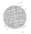
- the master electrode 100 is formed by an at least partly electrically semiconducting circular carrier element 101, such as a Si wafer.
- the size of the carrier element may vary depending on the dimensions of the ECPR equipment to be used, but is typically of the size of standard semiconducting wafers, such as 100, 150, 200, 250, or 300 mm (4, 6, 8, 10, or 12 inches) in diameter.
- the upper surface 102, or front side of the master electrode 100 is divided into a plurality of rectangular segments 103, each segment 103 defining a device pattern, such as a chip layer, to be transferred to a substrate during an ECPR process.
- the distribution of the rectangular segments 103 forms a device area 130 which is terminated by a circular periphery forming an interface to a surrounding passivated area 140, having an annular shape.
- the passivated area 140 is formed by oxidizing the outer part of the device area 130, such that the topographical pattern of the outer part of the device area 130 is provided with an oxide layer for preventing plating at this region.
- the passivated area is surrounded by an edge region 150 being recessed relative the device area and the passivated area.
- the recessed part 119 of the carrier element 101 is formed in order to provide enough space for arranging an electrode (not shown) to provide electrical contact to the edge of the substrate to be plated during ECPR, without touching or damaging the master electrode.
- the surfaces of the recessed region 119 are passivated with an insulating material such as silicon dioxide or silicon nitride so that the electrodes connected to the substrate are not electrically connected to the master electrode.
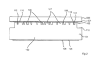
- a side view of the master electrode 100 is schematically shown when arranged in close contact with a substrate 200 to be plated during ECPR.
- the carrier element 101 extends between a back side 104 and a front side 105, in such a way that electrical current is able to flow between the back side 104 and the front side 105.
- an electrode layer 106 of an electrically conducting material is arranged at the back side 104.
- the electrode layer 106 may be formed by nickel silicide, or any other conducting material being suitable for a back side electrode layer during ECPR.
- the front side 105 comprises a topographical pattern 107 with an at least partly electrically insulating top 108.
- the topographical pattern 107 is forming a plurality of electrochemical cells 109. That is, the planar surface extending between two adjacent electrochemical cells 109 is covered by an electrically insulating layer 110.
- Each electrochemical cell comprises a bottom 111 and at least one side wall 112 extending from the bottom 111 to the electrically insulating top 108.
- the sidewall of the cavity is covered with an electrically insulating layer which extends from the surface insulating layer 110 to the point at which the sidewall meets the bottom of the cavity 111.
- the bottom 111 has an electrically conducting surface 113 being conductively connected to the electrically conducting electrode surface 106 on the back side 104 by means of the carrier element 101.
- the carrier element 101 is disposed between the conducting electrode surface 106 and the electrically conducting surface 113.
- the conductive surface 113 is formed by any material being suitable as an anode/cathode in the ECPR.
- the conductive surface 113 may be formed by a self-aligned silicidation process.
- the topographical pattern 107 extends from the center of the carrier element 101 radially towards the edge of the carrier element 101 and ends at a circular periphery arranged at a specific distance from the edge of the carrier element.
- the outer area 119 of the carrier element 101 not being occupied by the topographical pattern 107 is recessed such that the outer area is not in close contact with a substrate during ECPR.
- the radial distance between the outer periphery of the topographical pattern 107 and the edge of the carrier element 101 is between 2.5 mm and 10 mm, and the width of the recessed part 119 of the carrier element is preferably 2 to 5 mm.
- the annular recess 119 is formed by using a resist mask and a deep silicon etch or by mechanical grinding or dicing of the carrier element 101.
- the depth of the recess region 119 is between 100 and 200 microns deep.
- the recessed part 119 of the carrier element 101 is formed in order to provide enough space for arranging an electrode at the edge of the substrate to be plated during ECPR, without touching or damaging the master electrode.
- the surfaces of the region outside of the topological pattern 107 including the recessed portion 119 of the carrier element and the edge of the carrier element 101 are passivated with an electrically insulating material. This prevents unwanted parasitic current flowing at the edges of carrier during the ECPR pattern transfer.
- the master electrode 100 is put in close contact with a substrate 200 to be plated.
- the substrate 200 is provided with a seed layer 201 of electrically conductive material, such that conductive ions may be plated onto said seed layer 201.
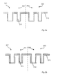
- FIGs. 3a-g side views of an ECPR master electrode 300 are shown.
- the master electrode 300 has a topographical pattern 307 on the front side, i.e. the side of the master electrode 300 that will face the substrate to be plated during ECPR.
- the topographical pattern 307 is distributed circularly across a device area 301.
- the device area 301 comprises a plurality of adjacently arranged rectangular chips which extend towards the edge of the master electrode.
- a recessed region is formed in accordance with what has previously been described.
- the passivated area 302 of the topographical pattern 307 comprises a distribution of cavities in which the conduction path through the electrolyte is blocked. In these cavities a selectively grown thermal oxide prevents formation of the conductive layer in the bottom of the cavities. Hence in the passivated area no ECPR transfer takes place even though there is electrolyte in the cavities of the electrochemical cells.
- the pattern transfer during the ECPR process is thus defined entirely by the circular device area 301.
- Said electrochemical cells of the passivated area 302 may be defined using a circular mask or lithographic edge bead removal process, which will be described in further details below.
- the thickness of the oxide is preferably in the range 500nm to 1000nm. Consequently, the current flow will be uniform at the edge of the device area 301 during ECPR, and the plating thickness will thus be homogenous over the complete device area 301.
- the master electrode 300 of Fig. 3 is preferably manufactured by a lithographic process involving two separate exposure steps.
- the device area 301 is provided by stepper technology, which is a well established process for providing rectangular chip pattern on a semiconducting carrier element, such as a Si wafer.
- a stepper or scanner may here be used for providing the chip pattern with low defectivity and high resolution such that the topographic pattern 307 defining the chips extends to the edge of the carrier element.
- Figure 3a further shows representative cells or cavities of the topographic pattern 307 in the carrier element.
- the surface of the carrier element is passivated with insulating material 310 and the sidewalls of the cavities with a further insulating material 311 such that the complete front surface of the carrier element, except for the area of the bottom of each cell, is covered by said insulating material.
- the insulating material 310 is also used as an etch mask during the provision of the electrochemical cells.
- An edge bead removal process during the lithographic process commonly defines the proximity of the device area 301 to the edge of the master electrode which is typically in the range of 1 to 4 mm from the edge.
- four cavities, which later will be processed as electrochemical cells, are shown.
- the cavities on the left side of the dashed line lie within the device area 303 while the cavities on the right side of the dashed line lie within the passivated area 302.
- a third layer 314, preferably CVD silicon nitride is first deposited as shown in Fig. 3b .
- Silicon nitride is a commonly used semiconductor material and provides a film with excellent step coverage and extremely high resistance to thermal oxidation.
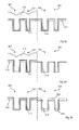
- a second lithographic process is used for defining the circular periphery of the passivated area 302.
- This step is performed by coating a thick layer of resist 318 on the front side of the carrier element, and a subsequent exposure and development of the outer periphery of the master electrode.
- the thickness of the resist 318 should preferably be sufficient to at least partially fill the depth of the topographical pattern 307.
- the photoresist may be exposed with a mask aligner using a circular chrome pattern on the mask.
- a further method of achieving the cicular pattern in the thick photoresist may be to use an optical or chemical edge bead removal process commonly found on spin coater type semiconductor equipment.
- the silicon nitride is then etched using e.g. a RIE etch tool.
- the RIE etch removes the silicon nitride in the bottom of the trenches and the surface dielectrics as shown in Fig. 3d .
- This type of etch is highly anisotropic and does not attack the silicon nitride on the sidewalls of the cavities.
- the carrier element of the master electrode 300 may be subjected to a high temperature oxidation process as shown in Fig. 3e .
- the preferred thickness of this thermal oxide 320 is in the range 500-1000 nm, although other thicknesses of course may be considered as well.
- the silicon nitride layer 314 will prevent oxidation of the central portion of the master electrode 300, i.e. the device area 301, while the outer portion of the master electrode 300, i.e. the passivated area 302, will be oxidized.
- the recessed region of the master electrode 300 and the bevel/edge of the carrier element will be oxidized.
- the conducting layer is formed in the cavities for forming the electrochemical cells of the topographic pattern 307.
- the silicon nitride layer 314 of the device area 301 is first removed using e.g. an unmasked or blanket RIE process as depicted in Fig. 3f .
- the thermally grown oxide 312 on the surface of the master electrode 300, as well as the oxide 320 arranged in the bottom of the cavities outside the device area 301 is etched only slightly during this etch process. This is due to the very large differential thicknesses and the chemistry used in the RIE process, which provides high SiN to SiO 2 selectivity.
- the thick thermal oxide 320 will block the formation of the conductive layer 322 in the bottom of the cavities as shown in Fig. 3g .
Landscapes
- Chemical & Material Sciences (AREA)
- Engineering & Computer Science (AREA)
- Chemical Kinetics & Catalysis (AREA)
- Electrochemistry (AREA)
- Materials Engineering (AREA)
- Metallurgy (AREA)
- Organic Chemistry (AREA)
- Micromachines (AREA)
- Electrodes Of Semiconductors (AREA)
Abstract
Description
- The present invention relates to an ECPR master electrode, and a method for providing such master electrode. More particularly, the present invention relates to a circular ECPR master electrode.
-
WO 02/103085 WO 2007058603 relate to an electrochemical pattern replication process, ECPR, and the construction of a master electrode for production of appliances involving micro and nano structures using ECPR. An etching or plating pattern, which is defined by the master electrode, is replicated on an electrically conductive material, commonly denoted as a substrate. During ECPR, the master electrode is put in close contact with the substrate and the etching/plating pattern is directly transferred onto the substrate by an etching/plating process. The contact etching/plating process is performed in local etching/plating cells, which are formed in cavities between the master electrode and the substrate. - The cavities are provided as electrochemical cells having an open end at the upper surface of the master electrode, and extending downwards. Hence, the upper surface of the master electrode includes a topographical pattern defining at least one electrochemical cell, wherein the bottom of each cell is provided with an electrically conducting material. During ECPR, each cell is filled with an electrolyte solution, for allowing conducting ions of the conducting material to be transferred from the bottom of each cell to the substrate to be patterned.
- The area between the electrochemical cells, i.e. the uppermost area of the topographical pattern of the master electrode is provided with an insulating layer for preventing unwanted parasitic currents during the ECPR process. Hence, ECPR will only provide pattern transfer at the positions being defined by the electrochemical cells.
- Before the master electrode is used in the ECPR, the electrochemical cells need to be prefilled with a conductive material. Usually, the thickness of the prefilled material is in the range of 0,5 to 10 micrometers, depending on the specific application. During the ECPR the conductive material is transferred from the bottom of the electrochemical cells of the master electrode to the substrate being plated. Thus, when the master electrode is separated from the processed substrate the prefilled conductive material is arranged on the substrate.
- The master electrode may be made of a carrier element of a durable material, since the master electrode should be used for a plurality of processes of etching or plating. One such material is Si, which allows the master electrode to be manufactured by well established and high yield semiconductor processes. Consequently, in many cases circular Si wafers form the carrier elements of ECPR master electrodes.
- For the chip industry, the topographical pattern of the master electrode may be arranged in a planar distribution across the master electrode surface, wherein the planar distribution includes a number of rectangular sub-areas. In such application, each rectangular sub-area may define a chip. Hence, the master electrode may be provided with a topographical pattern being periodic and defining a plurality of adjacently arranged rectangular chips. The rectangular shape of each chip is usually necessary because of the need for facilitated dicing and chip separation later in the device manufacturing process.
- During ECPR, current will flow radially through the master electrode to the seeded substrate and out via an external connection at the edge of the substrate. If the pattern density across the master electrode is exhibiting variations close to the edge of the circular carrier element, this may result in uneven plating thickness across the substrate being processed by ECPR due to non-uniform current flow. Thus, the chips having a position corresponding to the central part of the master electrode will be different from the chips having a position corresponding to the more peripheral part of the master electrode. Quality may therefore vary between different chips.
- Accordingly, the present invention seeks to mitigate, alleviate or eliminate one or more of the above-identified deficiencies and to provide an improved ECPR master electrode as well as a method for manufacturing such master electrode.
- It is an object of the present invention to provide a circular ECPR master electrode to be used in rectangular chip fabrication.
- It is a further object of the present invention to provide a method for manufacturing such master electrode using a simple lithographic process, which may be done by standard semiconductor process equipment.
- It is a further object of the present invention to provide a method for manufacturing such master electrode while allowing for uniform quality of the manufactured chips.
- It is an idea of the present invention to provide a circular ECPR master electrode having a topographical pattern defining electrochemical cells arranged in a periodic rectangular pattern, and a passivated area at the periphery of said topographical pattern such that said topographical pattern has a circular distribution.
- According to a first aspect of the invention a method for providing an ECPR master electrode is provided. The method comprises the step of providing a circular carrier element having an electrically conducting electrode surface on a back side and a topographical pattern with an at least partly electrically insulating top on a front side of said carrier element, said topographical pattern comprising a plurality of electrochemical cells in said carrier element, each one of said electrochemical cells comprising a bottom and at least one side wall, said bottom having an electrically conducting surface being conductively connected to the electrically conducting electrode surface on the back side through the carrier element, wherein the step of providing said topographical pattern comprises distributing said topographical pattern across a device area extending radially from the centre of the carrier element towards the periphery of said carrier element, and passivating a peripheral part of said device area by arranging an electrically insulating layer on top of said peripheral part of said device area.
- Distributing the topographical pattern across a device area may comprise providing a plurality of rectangular chip areas, each chip area is forming a portion of said topographical pattern. Distributing the topographical pattern across a device area may further comprise covering the complete front side of said carrier element with said topographical pattern. Hence, scanner or stepper technology may be used for defining the topographical pattern.
- The step of passivating a peripheral part of said device area may comprise providing an oxide mask on top of a portion of said device area; oxidizing said front side of said carrier element; and removing said oxide mask from said device area. Providing an oxide mask may comprise providing a first layer of silicon nitride on top of said device area; providing a resist layer on top of said layer of silicon nitride; removing a peripheral part of said resist layer; and etching through the first layer of silicon nitride using the remaining resist layer as an etch mask. This is advantageous in that the passivation is achieved with good selectivity and simple processing, since the steps used are commonly known within the semiconducting industry.
- The step of etching through the first layer of silicon nitride may be performed by an anisotropic process. Hence, accurate transfer of patterns is provided.
- The method may further comprise the step of providing an annular recess at said peripheral part, which is advantageous in that enough room is provided for contacting the substrate during ECPR.
- According to a second aspect, and ECPR master electrode is provided. The master electrode comprises a circular carrier element having an electrically conducting electrode surface on a back side and a topographical pattern with an at least partly electrically insulating top on a front side of said carrier element, said topographical pattern comprising a plurality of electrochemical cells in said carrier element, each one of said electrochemical cells comprising a bottom and at least one side wall, said bottom having an electrically conducting surface being conductively connected to the electrically conducting electrode surface on the back side through the carrier element, wherein said topographical pattern is distributed across a circular device area comprising a plurality of rectangular chip areas, and a passivated area surrounding said device area.
- Said passivated area may comprise an oxide layer on top of said topographical pattern.
- The carrier element may comprise an annular recess outside the passivated area.
- Said annular recess may extend from the outer circular periphery of the passivated area to the edge of the carrier element.
- The advantages of the first aspect of the invention are also applicable for the second aspect of the invention.
- Hereinafter, the invention will be described with reference to the appended drawings, wherein:
-
Fig. 1 is a top view of an ECPR master electrode according to an embodiment; -
Fig. 2 is a side view of a master electrode and a substrate during ECPR; and -
Fig. 3a-g show the manufacturing process of a master electrode according to an embodiment. - Below, several embodiments of the invention will be described with references to the drawings. These embodiments are described in illustrating purpose in order to enable a skilled person to carry out the invention and to disclose the best mode. However, such embodiments do not limit the invention, but other combinations of the different features are possible within the scope of the invention.
- Some general remarks are given below with regard to the master electrode and methods of forming the master electrode. Several methods are described for forming a master electrode that can be used for producing one or multiple layers of structures of one or multiple materials including using the ECPR technology described below. The methods generally include: forming a master electrode from a carrier element which is conducting and/or semiconducting in at least some parts; forming a conducting electrode layer which functions as anode in ECPR plating and cathode in ECPR etching on a front side of the master electrode; and forming an insulating pattern layer that defines the cavities in which ECPR etching or plating can occur in the ECPR process on said front side, such that conducting electrode surface(s) is/are obtained in the bottom of the cavities; in a way that makes possible electrical contact from an external power supply to the back side of the master electrode for allowing electron transfer through the master electrode to the front side thereof to the conducing electrode surface(s), such that said surface(s) will constitute anode(s) in ECPR plating and cathode(s) in ECPR etching.
- Now referring to
Fig. 1 , a top view of amaster electrode 100 is shown. Themaster electrode 100 is formed by an at least partly electrically semiconductingcircular carrier element 101, such as a Si wafer. The size of the carrier element may vary depending on the dimensions of the ECPR equipment to be used, but is typically of the size of standard semiconducting wafers, such as 100, 150, 200, 250, or 300 mm (4, 6, 8, 10, or 12 inches) in diameter. Theupper surface 102, or front side of themaster electrode 100 is divided into a plurality ofrectangular segments 103, eachsegment 103 defining a device pattern, such as a chip layer, to be transferred to a substrate during an ECPR process. - The distribution of the
rectangular segments 103 forms a device area 130 which is terminated by a circular periphery forming an interface to a surrounding passivated area 140, having an annular shape. The passivated area 140 is formed by oxidizing the outer part of the device area 130, such that the topographical pattern of the outer part of the device area 130 is provided with an oxide layer for preventing plating at this region. - The passivated area is surrounded by an
edge region 150 being recessed relative the device area and the passivated area. The recessedpart 119 of thecarrier element 101 is formed in order to provide enough space for arranging an electrode (not shown) to provide electrical contact to the edge of the substrate to be plated during ECPR, without touching or damaging the master electrode. Furthermore, the surfaces of the recessedregion 119 are passivated with an insulating material such as silicon dioxide or silicon nitride so that the electrodes connected to the substrate are not electrically connected to the master electrode. - Now turning to
Fig. 2 , a side view of themaster electrode 100 is schematically shown when arranged in close contact with asubstrate 200 to be plated during ECPR. It should be noted that the master electrode and the substrate shown in this figure are not to scale, but shown only to illustrate different features in a suitable way. Thecarrier element 101 extends between aback side 104 and a front side 105, in such a way that electrical current is able to flow between theback side 104 and the front side 105. At theback side 104, anelectrode layer 106 of an electrically conducting material is arranged. Theelectrode layer 106 may be formed by nickel silicide, or any other conducting material being suitable for a back side electrode layer during ECPR. - The front side 105 comprises a
topographical pattern 107 with an at least partly electrically insulatingtop 108. Thetopographical pattern 107 is forming a plurality ofelectrochemical cells 109. That is, the planar surface extending between two adjacentelectrochemical cells 109 is covered by an electrically insulatinglayer 110. - Each electrochemical cell comprises a bottom 111 and at least one
side wall 112 extending from the bottom 111 to the electrically insulatingtop 108. The sidewall of the cavity is covered with an electrically insulating layer which extends from thesurface insulating layer 110 to the point at which the sidewall meets the bottom of thecavity 111. The bottom 111 has an electrically conductingsurface 113 being conductively connected to the electrically conductingelectrode surface 106 on theback side 104 by means of thecarrier element 101. Thus, thecarrier element 101 is disposed between the conductingelectrode surface 106 and the electrically conductingsurface 113. Theconductive surface 113 is formed by any material being suitable as an anode/cathode in the ECPR. Preferably, theconductive surface 113 may be formed by a self-aligned silicidation process. - The
topographical pattern 107 extends from the center of thecarrier element 101 radially towards the edge of thecarrier element 101 and ends at a circular periphery arranged at a specific distance from the edge of the carrier element. Theouter area 119 of thecarrier element 101 not being occupied by thetopographical pattern 107 is recessed such that the outer area is not in close contact with a substrate during ECPR. Preferably, the radial distance between the outer periphery of thetopographical pattern 107 and the edge of thecarrier element 101 is between 2.5 mm and 10 mm, and the width of the recessedpart 119 of the carrier element is preferably 2 to 5 mm. Theannular recess 119 is formed by using a resist mask and a deep silicon etch or by mechanical grinding or dicing of thecarrier element 101. Preferably the depth of therecess region 119 is between 100 and 200 microns deep. The recessedpart 119 of thecarrier element 101 is formed in order to provide enough space for arranging an electrode at the edge of the substrate to be plated during ECPR, without touching or damaging the master electrode. - The surfaces of the region outside of the
topological pattern 107 including the recessedportion 119 of the carrier element and the edge of thecarrier element 101 are passivated with an electrically insulating material. This prevents unwanted parasitic current flowing at the edges of carrier during the ECPR pattern transfer. - During ECPR, the
master electrode 100 is put in close contact with asubstrate 200 to be plated. Thesubstrate 200 is provided with aseed layer 201 of electrically conductive material, such that conductive ions may be plated onto saidseed layer 201. - Now turning to
Figs. 3a-g , side views of anECPR master electrode 300 are shown. Themaster electrode 300 has atopographical pattern 307 on the front side, i.e. the side of themaster electrode 300 that will face the substrate to be plated during ECPR. Thetopographical pattern 307 is distributed circularly across adevice area 301. Thedevice area 301 comprises a plurality of adjacently arranged rectangular chips which extend towards the edge of the master electrode. At the edge of the carrier element a recessed region is formed in accordance with what has previously been described. - The passivated
area 302 of thetopographical pattern 307 comprises a distribution of cavities in which the conduction path through the electrolyte is blocked. In these cavities a selectively grown thermal oxide prevents formation of the conductive layer in the bottom of the cavities. Hence in the passivated area no ECPR transfer takes place even though there is electrolyte in the cavities of the electrochemical cells. The pattern transfer during the ECPR process is thus defined entirely by thecircular device area 301. - Said electrochemical cells of the passivated
area 302 may be defined using a circular mask or lithographic edge bead removal process, which will be described in further details below. The thickness of the oxide is preferably in the range 500nm to 1000nm. Consequently, the current flow will be uniform at the edge of thedevice area 301 during ECPR, and the plating thickness will thus be homogenous over thecomplete device area 301. - The
master electrode 300 ofFig. 3 is preferably manufactured by a lithographic process involving two separate exposure steps. At a first step, shown inFig. 3a , thedevice area 301 is provided by stepper technology, which is a well established process for providing rectangular chip pattern on a semiconducting carrier element, such as a Si wafer. A stepper or scanner may here be used for providing the chip pattern with low defectivity and high resolution such that thetopographic pattern 307 defining the chips extends to the edge of the carrier element. -
Figure 3a further shows representative cells or cavities of thetopographic pattern 307 in the carrier element. The surface of the carrier element is passivated with insulatingmaterial 310 and the sidewalls of the cavities with a further insulatingmaterial 311 such that the complete front surface of the carrier element, except for the area of the bottom of each cell, is covered by said insulating material. Preferably, the insulatingmaterial 310 is also used as an etch mask during the provision of the electrochemical cells. - An edge bead removal process during the lithographic process commonly defines the proximity of the
device area 301 to the edge of the master electrode which is typically in the range of 1 to 4 mm from the edge. Referring back tofigure 3a , four cavities, which later will be processed as electrochemical cells, are shown. The cavities on the left side of the dashed line lie within the device area 303 while the cavities on the right side of the dashed line lie within the passivatedarea 302. - In order to create a circular termination to the pattern 303 a
third layer 314, preferably CVD silicon nitride, is first deposited as shown inFig. 3b . Silicon nitride is a commonly used semiconductor material and provides a film with excellent step coverage and extremely high resistance to thermal oxidation. - Referring to
Fig. 3c , as a subsequent step, a second lithographic process is used for defining the circular periphery of the passivatedarea 302. This step is performed by coating a thick layer of resist 318 on the front side of the carrier element, and a subsequent exposure and development of the outer periphery of the master electrode. During this step, the thickness of the resist 318 should preferably be sufficient to at least partially fill the depth of thetopographical pattern 307. - In order to create a circular resist pattern the photoresist may be exposed with a mask aligner using a circular chrome pattern on the mask.
- A further method of achieving the cicular pattern in the thick photoresist may be to use an optical or chemical edge bead removal process commonly found on spin coater type semiconductor equipment.
- After the resist is patterned the silicon nitride is then etched using e.g. a RIE etch tool. The RIE etch removes the silicon nitride in the bottom of the trenches and the surface dielectrics as shown in
Fig. 3d . This type of etch is highly anisotropic and does not attack the silicon nitride on the sidewalls of the cavities. - After etching the silicon nitride and stripping of the photoresist the carrier element of the
master electrode 300 may be subjected to a high temperature oxidation process as shown inFig. 3e . The preferred thickness of thisthermal oxide 320 is in the range 500-1000 nm, although other thicknesses of course may be considered as well. Thesilicon nitride layer 314 will prevent oxidation of the central portion of themaster electrode 300, i.e. thedevice area 301, while the outer portion of themaster electrode 300, i.e. the passivatedarea 302, will be oxidized. At the same time, the recessed region of themaster electrode 300 and the bevel/edge of the carrier element will be oxidized. - In the following steps the conducting layer is formed in the cavities for forming the electrochemical cells of the
topographic pattern 307. Thesilicon nitride layer 314 of thedevice area 301 is first removed using e.g. an unmasked or blanket RIE process as depicted inFig. 3f . The thermally grown oxide 312 on the surface of themaster electrode 300, as well as theoxide 320 arranged in the bottom of the cavities outside thedevice area 301 is etched only slightly during this etch process. This is due to the very large differential thicknesses and the chemistry used in the RIE process, which provides high SiN to SiO2 selectivity. The thickthermal oxide 320 will block the formation of theconductive layer 322 in the bottom of the cavities as shown inFig. 3g . - It is readily understood that all references to lower/upper are merely for illustrative purposes, without any limiting effect on the scope of protection. Also, it should be noted that the dimensions of the different features and layers shown in the figures are not to scale, but should be interpreted only for illustrative purpose. All references in this application to actual values, such as layer thicknesses etc, should also only be read as examples of suitable dimensions.
- In the claims, the term "comprises/comprising" does not exclude the presence of other elements or steps. Additionally, although individual features may be included in different claims, these may possibly advantageously be combined, and the inclusion in different claims does not imply that a combination of features is not feasible and/or advantageous. In addition, singular references do not exclude a plurality. The terms "a", "an", "first", "second" etc do not preclude a plurality. Reference signs in the claims are provided merely as a clarifying example and shall not be construed as limiting the scope of the claims in any way.
Claims (12)
- A method for providing an ECPR master electrode, comprising the step of:providing a circular carrier element having an electrically conducting electrode surface on a back side and a topographical pattern with an at least partly electrically insulating top on a front side of said carrier element, said topographical pattern comprising a plurality of electrochemical cells in said carrier element, each one of said electrochemical cells comprising a bottom and at least one side wall, said bottom having an electrically conducting surface being conductively connected to the electrically conducting electrode surface on the back side through the carrier element,wherein the step of providing said topographical pattern comprises:distributing said topographical pattern across a device area extending radially from the centre of the carrier element towards the periphery of said carrier element, andpassivating a peripheral part of said device area by arranging an electrically insulating layer on top of said peripheral part of said device area.
- The method according to claim 1, wherein said electrically insulating layer is an oxide layer.
- The method according to claim 1 or 2, wherein distributing the topographical pattern across a device area comprises providing a plurality of rectangular chip areas, each chip area is forming a portion of said topographical pattern.
- The method according to any of the preceding claims, wherein distributing the topographical pattern across a device area comprises covering the complete front side of said carrier element with said topographical pattern.
- The method according to any of the preceding claims, wherein the step of passivating a peripheral part of said device area comprises:providing an oxide mask on top of a portion of said device area;oxidizing said front side of said carrier element; andremoving said oxide mask from said device area.
- The method according to claim 5, wherein the step of providing an oxide mask comprises
providing a first layer of silicon nitride on top of said device area;
providing a resist layer on top of said layer of silicon nitride;
removing a peripheral part of said resist layer; and
etching through the first layer of silicon nitride using the remaining resist layer as an etch mask. - The method according to claim 6, wherein the step of etching through the first layer of silicon nitride is performed by an anisotropic process.
- The method according to any of the preceding claims, further comprising the step of providing an annular recess at said peripheral part.
- An ECPR master electrode (100, 300), comprising
a circular carrier element (101) having an electrically conducting electrode surface (106) on a back side (104) and a topographical pattern (107, 307) with an at least partly electrically insulating top (108) on a front side (105) of said carrier element (101),
said topographical pattern comprising a plurality of electrochemical cells (109) in said carrier element (101), each one of said electrochemical cells comprising a bottom (111) and at least one side wall (112), said bottom having an electrically conducting surface (113) being conductively connected to the electrically conducting electrode surface (106) on the back side (104) through the carrier element (101), wherein
said topographical pattern (107, 307) is distributed across a circular device area (130, 301) comprising a plurality of rectangular chip areas (103), and a passivated area (140, 302) surrounding said device area (130, 301). - The ECPR master electrode according to claim 9, wherein said passivated area (140, 302) comprises an oxide layer (320) on top of said topographical pattern (107,307).
- The ECPR master electrode according to claim 8 or 9, wherein the carrier element (101) comprises an annular recess outside the passivated area (140, 302).
- The ECPR master electrode according to claim 11, wherein said annular recess extends from the outer circular periphery of the passivated area (140, 302) to the edge of the carrier element (101).
Priority Applications (1)
| Application Number | Priority Date | Filing Date | Title |
|---|---|---|---|
| EP12171198.0A EP2533272B1 (en) | 2011-06-07 | 2012-06-07 | An ecpr master electrode, and a method for providing such master electrode |
Applications Claiming Priority (2)
| Application Number | Priority Date | Filing Date | Title |
|---|---|---|---|
| EP11290259 | 2011-06-07 | ||
| EP12171198.0A EP2533272B1 (en) | 2011-06-07 | 2012-06-07 | An ecpr master electrode, and a method for providing such master electrode |
Publications (2)
| Publication Number | Publication Date |
|---|---|
| EP2533272A1 true EP2533272A1 (en) | 2012-12-12 |
| EP2533272B1 EP2533272B1 (en) | 2014-03-12 |
Family
ID=46177375
Family Applications (1)
| Application Number | Title | Priority Date | Filing Date |
|---|---|---|---|
| EP12171198.0A Not-in-force EP2533272B1 (en) | 2011-06-07 | 2012-06-07 | An ecpr master electrode, and a method for providing such master electrode |
Country Status (1)
| Country | Link |
|---|---|
| EP (1) | EP2533272B1 (en) |
Citations (3)
| Publication number | Priority date | Publication date | Assignee | Title |
|---|---|---|---|---|
| WO2002103085A1 (en) | 2001-06-15 | 2002-12-27 | Replisaurus Hb | Method and electrode for defining and replicating structures in conducting materials |
| US20040182716A1 (en) * | 2002-11-26 | 2004-09-23 | Microfabrica Inc. | Method for electrochemically forming structures including non-parallel mating of contact masks and substrates |
| JP2005256110A (en) * | 2004-03-12 | 2005-09-22 | Seiko Instruments Inc | Structure and manufacturing method of electroforming mold and electroforming method using the electroforming mold |
-
2012
- 2012-06-07 EP EP12171198.0A patent/EP2533272B1/en not_active Not-in-force
Patent Citations (3)
| Publication number | Priority date | Publication date | Assignee | Title |
|---|---|---|---|---|
| WO2002103085A1 (en) | 2001-06-15 | 2002-12-27 | Replisaurus Hb | Method and electrode for defining and replicating structures in conducting materials |
| US20040182716A1 (en) * | 2002-11-26 | 2004-09-23 | Microfabrica Inc. | Method for electrochemically forming structures including non-parallel mating of contact masks and substrates |
| JP2005256110A (en) * | 2004-03-12 | 2005-09-22 | Seiko Instruments Inc | Structure and manufacturing method of electroforming mold and electroforming method using the electroforming mold |
Also Published As
| Publication number | Publication date |
|---|---|
| EP2533272B1 (en) | 2014-03-12 |
Similar Documents
| Publication | Publication Date | Title |
|---|---|---|
| US8367500B1 (en) | Method of forming self aligned contacts for a power MOSFET | |
| EP4386825A1 (en) | Separation gate power device and manufacturing method therefor | |
| US20160190154A1 (en) | Methods for making a trim-rate tolerant self-aligned contact via structure array | |
| CN104112768B (en) | Semiconductor device and its termination region structure | |
| KR100192549B1 (en) | Manufacturing method and structure of mask | |
| US20190252614A1 (en) | Mother plate, method for manufacturing mother plate, method for manufacturing mask, and oled pixel deposition method | |
| CN111211157A (en) | Fast recovery diode and preparation method thereof | |
| CN106653831A (en) | High density low voltage trench power MOS device and method of manufacturing same | |
| CN104900719A (en) | Trench Schottky diode terminal structure and preparation method thereof | |
| KR20210008920A (en) | Anodized aluminum oxide as a hard mask for plasma etching | |
| US20150228603A1 (en) | Semiconductor Constructions and Methods of Planarizing Across a Plurality of Electrically Conductive Posts | |
| JP2005256110A (en) | Structure and manufacturing method of electroforming mold and electroforming method using the electroforming mold | |
| EP2533272B1 (en) | An ecpr master electrode, and a method for providing such master electrode | |
| US7671446B2 (en) | Semiconductor capacitor and manufacturing method | |
| US20110089522A1 (en) | Semiconductor device and method of manufacturing the same | |
| EP2533271B1 (en) | An ecpr master electrode, and a method for providing such master electrode | |
| CN204905205U (en) | Integrated vacuum microelectronics structure | |
| US20080149490A1 (en) | Electroplating on ultra-thin seed layers | |
| CN103022155A (en) | Groove MOS (metal oxide semiconductor) structure Schottky diode and preparation method thereof | |
| EP2533273B1 (en) | An ECPR master electrode, and a method for providing such master electrode | |
| CN203733800U (en) | Semiconductor device and terminal region structure thereof | |
| TW201322375A (en) | Resistive ram device having improved switching characteristics | |
| CN115566078A (en) | A semiconductor dielectric layer structure and manufacturing method | |
| CN104425654B (en) | Engraving method | |
| CN114446784A (en) | Silicon carbide junction barrier Schottky diode and preparation method thereof |
Legal Events
| Date | Code | Title | Description |
|---|---|---|---|
| PUAI | Public reference made under article 153(3) epc to a published international application that has entered the european phase |
Free format text: ORIGINAL CODE: 0009012 |
|
| AK | Designated contracting states |
Kind code of ref document: A1 Designated state(s): AL AT BE BG CH CY CZ DE DK EE ES FI FR GB GR HR HU IE IS IT LI LT LU LV MC MK MT NL NO PL PT RO RS SE SI SK SM TR |
|
| AX | Request for extension of the european patent |
Extension state: BA ME |
|
| RAP1 | Party data changed (applicant data changed or rights of an application transferred) |
Owner name: CENTRE DE RECHERCHE PUBLIC - GABRIEL LIPPMANN |
|
| 17P | Request for examination filed |
Effective date: 20130606 |
|
| RBV | Designated contracting states (corrected) |
Designated state(s): AL AT BE BG CH CY CZ DE DK EE ES FI FR GB GR HR HU IE IS IT LI LT LU LV MC MK MT NL NO PL PT RO RS SE SI SK SM TR |
|
| REG | Reference to a national code |
Ref country code: DE Ref legal event code: R079 Ref document number: 602012000996 Country of ref document: DE Free format text: PREVIOUS MAIN CLASS: H01L0021288000 Ipc: C25D0017120000 |
|
| RIC1 | Information provided on ipc code assigned before grant |
Ipc: C25D 17/12 20060101AFI20130821BHEP Ipc: H01L 21/288 20060101ALI20130821BHEP |
|
| GRAP | Despatch of communication of intention to grant a patent |
Free format text: ORIGINAL CODE: EPIDOSNIGR1 |
|
| INTG | Intention to grant announced |
Effective date: 20131021 |
|
| GRAS | Grant fee paid |
Free format text: ORIGINAL CODE: EPIDOSNIGR3 |
|
| GRAA | (expected) grant |
Free format text: ORIGINAL CODE: 0009210 |
|
| AK | Designated contracting states |
Kind code of ref document: B1 Designated state(s): AL AT BE BG CH CY CZ DE DK EE ES FI FR GB GR HR HU IE IS IT LI LT LU LV MC MK MT NL NO PL PT RO RS SE SI SK SM TR |
|
| REG | Reference to a national code |
Ref country code: GB Ref legal event code: FG4D |
|
| REG | Reference to a national code |
Ref country code: CH Ref legal event code: EP |
|
| REG | Reference to a national code |
Ref country code: AT Ref legal event code: REF Ref document number: 656402 Country of ref document: AT Kind code of ref document: T Effective date: 20140315 |
|
| REG | Reference to a national code |
Ref country code: IE Ref legal event code: FG4D |
|
| REG | Reference to a national code |
Ref country code: DE Ref legal event code: R096 Ref document number: 602012000996 Country of ref document: DE Effective date: 20140424 |
|
| REG | Reference to a national code |
Ref country code: NL Ref legal event code: T3 |
|
| PG25 | Lapsed in a contracting state [announced via postgrant information from national office to epo] |
Ref country code: LT Free format text: LAPSE BECAUSE OF FAILURE TO SUBMIT A TRANSLATION OF THE DESCRIPTION OR TO PAY THE FEE WITHIN THE PRESCRIBED TIME-LIMIT Effective date: 20140312 Ref country code: NO Free format text: LAPSE BECAUSE OF FAILURE TO SUBMIT A TRANSLATION OF THE DESCRIPTION OR TO PAY THE FEE WITHIN THE PRESCRIBED TIME-LIMIT Effective date: 20140612 |
|
| REG | Reference to a national code |
Ref country code: AT Ref legal event code: MK05 Ref document number: 656402 Country of ref document: AT Kind code of ref document: T Effective date: 20140312 |
|
| REG | Reference to a national code |
Ref country code: LT Ref legal event code: MG4D |
|
| PG25 | Lapsed in a contracting state [announced via postgrant information from national office to epo] |
Ref country code: FI Free format text: LAPSE BECAUSE OF FAILURE TO SUBMIT A TRANSLATION OF THE DESCRIPTION OR TO PAY THE FEE WITHIN THE PRESCRIBED TIME-LIMIT Effective date: 20140312 Ref country code: CY Free format text: LAPSE BECAUSE OF FAILURE TO SUBMIT A TRANSLATION OF THE DESCRIPTION OR TO PAY THE FEE WITHIN THE PRESCRIBED TIME-LIMIT Effective date: 20140312 Ref country code: SE Free format text: LAPSE BECAUSE OF FAILURE TO SUBMIT A TRANSLATION OF THE DESCRIPTION OR TO PAY THE FEE WITHIN THE PRESCRIBED TIME-LIMIT Effective date: 20140312 |
|
| PG25 | Lapsed in a contracting state [announced via postgrant information from national office to epo] |
Ref country code: HR Free format text: LAPSE BECAUSE OF FAILURE TO SUBMIT A TRANSLATION OF THE DESCRIPTION OR TO PAY THE FEE WITHIN THE PRESCRIBED TIME-LIMIT Effective date: 20140312 Ref country code: LV Free format text: LAPSE BECAUSE OF FAILURE TO SUBMIT A TRANSLATION OF THE DESCRIPTION OR TO PAY THE FEE WITHIN THE PRESCRIBED TIME-LIMIT Effective date: 20140312 Ref country code: RS Free format text: LAPSE BECAUSE OF FAILURE TO SUBMIT A TRANSLATION OF THE DESCRIPTION OR TO PAY THE FEE WITHIN THE PRESCRIBED TIME-LIMIT Effective date: 20140312 |
|
| PG25 | Lapsed in a contracting state [announced via postgrant information from national office to epo] |
Ref country code: EE Free format text: LAPSE BECAUSE OF FAILURE TO SUBMIT A TRANSLATION OF THE DESCRIPTION OR TO PAY THE FEE WITHIN THE PRESCRIBED TIME-LIMIT Effective date: 20140312 Ref country code: BG Free format text: LAPSE BECAUSE OF FAILURE TO SUBMIT A TRANSLATION OF THE DESCRIPTION OR TO PAY THE FEE WITHIN THE PRESCRIBED TIME-LIMIT Effective date: 20140612 Ref country code: CZ Free format text: LAPSE BECAUSE OF FAILURE TO SUBMIT A TRANSLATION OF THE DESCRIPTION OR TO PAY THE FEE WITHIN THE PRESCRIBED TIME-LIMIT Effective date: 20140312 Ref country code: IS Free format text: LAPSE BECAUSE OF FAILURE TO SUBMIT A TRANSLATION OF THE DESCRIPTION OR TO PAY THE FEE WITHIN THE PRESCRIBED TIME-LIMIT Effective date: 20140712 Ref country code: RO Free format text: LAPSE BECAUSE OF FAILURE TO SUBMIT A TRANSLATION OF THE DESCRIPTION OR TO PAY THE FEE WITHIN THE PRESCRIBED TIME-LIMIT Effective date: 20140312 |
|
| PG25 | Lapsed in a contracting state [announced via postgrant information from national office to epo] |
Ref country code: ES Free format text: LAPSE BECAUSE OF FAILURE TO SUBMIT A TRANSLATION OF THE DESCRIPTION OR TO PAY THE FEE WITHIN THE PRESCRIBED TIME-LIMIT Effective date: 20140312 Ref country code: SK Free format text: LAPSE BECAUSE OF FAILURE TO SUBMIT A TRANSLATION OF THE DESCRIPTION OR TO PAY THE FEE WITHIN THE PRESCRIBED TIME-LIMIT Effective date: 20140312 Ref country code: PL Free format text: LAPSE BECAUSE OF FAILURE TO SUBMIT A TRANSLATION OF THE DESCRIPTION OR TO PAY THE FEE WITHIN THE PRESCRIBED TIME-LIMIT Effective date: 20140312 Ref country code: AT Free format text: LAPSE BECAUSE OF FAILURE TO SUBMIT A TRANSLATION OF THE DESCRIPTION OR TO PAY THE FEE WITHIN THE PRESCRIBED TIME-LIMIT Effective date: 20140312 |
|
| REG | Reference to a national code |
Ref country code: DE Ref legal event code: R097 Ref document number: 602012000996 Country of ref document: DE |
|
| PG25 | Lapsed in a contracting state [announced via postgrant information from national office to epo] |
Ref country code: PT Free format text: LAPSE BECAUSE OF FAILURE TO SUBMIT A TRANSLATION OF THE DESCRIPTION OR TO PAY THE FEE WITHIN THE PRESCRIBED TIME-LIMIT Effective date: 20140714 |
|
| REG | Reference to a national code |
Ref country code: DE Ref legal event code: R119 Ref document number: 602012000996 Country of ref document: DE |
|
| PLBE | No opposition filed within time limit |
Free format text: ORIGINAL CODE: 0009261 |
|
| STAA | Information on the status of an ep patent application or granted ep patent |
Free format text: STATUS: NO OPPOSITION FILED WITHIN TIME LIMIT |
|
| PG25 | Lapsed in a contracting state [announced via postgrant information from national office to epo] |
Ref country code: MC Free format text: LAPSE BECAUSE OF FAILURE TO SUBMIT A TRANSLATION OF THE DESCRIPTION OR TO PAY THE FEE WITHIN THE PRESCRIBED TIME-LIMIT Effective date: 20140312 Ref country code: DK Free format text: LAPSE BECAUSE OF FAILURE TO SUBMIT A TRANSLATION OF THE DESCRIPTION OR TO PAY THE FEE WITHIN THE PRESCRIBED TIME-LIMIT Effective date: 20140312 |
|
| 26N | No opposition filed |
Effective date: 20141215 |
|
| PG25 | Lapsed in a contracting state [announced via postgrant information from national office to epo] |
Ref country code: RS Free format text: LAPSE BECAUSE OF FAILURE TO SUBMIT A TRANSLATION OF THE DESCRIPTION OR TO PAY THE FEE WITHIN THE PRESCRIBED TIME-LIMIT Effective date: 20140903 |
|
| REG | Reference to a national code |
Ref country code: IE Ref legal event code: MM4A |
|
| REG | Reference to a national code |
Ref country code: DE Ref legal event code: R119 Ref document number: 602012000996 Country of ref document: DE Effective date: 20150101 Ref country code: DE Ref legal event code: R097 Ref document number: 602012000996 Country of ref document: DE Effective date: 20141215 |
|
| REG | Reference to a national code |
Ref country code: FR Ref legal event code: ST Effective date: 20150227 |
|
| PG25 | Lapsed in a contracting state [announced via postgrant information from national office to epo] |
Ref country code: IT Free format text: LAPSE BECAUSE OF FAILURE TO SUBMIT A TRANSLATION OF THE DESCRIPTION OR TO PAY THE FEE WITHIN THE PRESCRIBED TIME-LIMIT Effective date: 20140312 |
|
| PG25 | Lapsed in a contracting state [announced via postgrant information from national office to epo] |
Ref country code: IE Free format text: LAPSE BECAUSE OF NON-PAYMENT OF DUE FEES Effective date: 20140607 Ref country code: DE Free format text: LAPSE BECAUSE OF NON-PAYMENT OF DUE FEES Effective date: 20150101 |
|
| PG25 | Lapsed in a contracting state [announced via postgrant information from national office to epo] |
Ref country code: FR Free format text: LAPSE BECAUSE OF NON-PAYMENT OF DUE FEES Effective date: 20140630 |
|
| PG25 | Lapsed in a contracting state [announced via postgrant information from national office to epo] |
Ref country code: SI Free format text: LAPSE BECAUSE OF FAILURE TO SUBMIT A TRANSLATION OF THE DESCRIPTION OR TO PAY THE FEE WITHIN THE PRESCRIBED TIME-LIMIT Effective date: 20140312 |
|
| REG | Reference to a national code |
Ref country code: CH Ref legal event code: PL |
|
| PG25 | Lapsed in a contracting state [announced via postgrant information from national office to epo] |
Ref country code: MT Free format text: LAPSE BECAUSE OF FAILURE TO SUBMIT A TRANSLATION OF THE DESCRIPTION OR TO PAY THE FEE WITHIN THE PRESCRIBED TIME-LIMIT Effective date: 20140312 |
|
| PG25 | Lapsed in a contracting state [announced via postgrant information from national office to epo] |
Ref country code: SM Free format text: LAPSE BECAUSE OF FAILURE TO SUBMIT A TRANSLATION OF THE DESCRIPTION OR TO PAY THE FEE WITHIN THE PRESCRIBED TIME-LIMIT Effective date: 20140312 Ref country code: CH Free format text: LAPSE BECAUSE OF NON-PAYMENT OF DUE FEES Effective date: 20150630 Ref country code: LI Free format text: LAPSE BECAUSE OF NON-PAYMENT OF DUE FEES Effective date: 20150630 |
|
| PG25 | Lapsed in a contracting state [announced via postgrant information from national office to epo] |
Ref country code: GR Free format text: LAPSE BECAUSE OF FAILURE TO SUBMIT A TRANSLATION OF THE DESCRIPTION OR TO PAY THE FEE WITHIN THE PRESCRIBED TIME-LIMIT Effective date: 20140613 |
|
| PG25 | Lapsed in a contracting state [announced via postgrant information from national office to epo] |
Ref country code: TR Free format text: LAPSE BECAUSE OF FAILURE TO SUBMIT A TRANSLATION OF THE DESCRIPTION OR TO PAY THE FEE WITHIN THE PRESCRIBED TIME-LIMIT Effective date: 20140312 Ref country code: HU Free format text: LAPSE BECAUSE OF FAILURE TO SUBMIT A TRANSLATION OF THE DESCRIPTION OR TO PAY THE FEE WITHIN THE PRESCRIBED TIME-LIMIT; INVALID AB INITIO Effective date: 20120607 |
|
| GBPC | Gb: european patent ceased through non-payment of renewal fee |
Effective date: 20160607 |
|
| PG25 | Lapsed in a contracting state [announced via postgrant information from national office to epo] |
Ref country code: GB Free format text: LAPSE BECAUSE OF NON-PAYMENT OF DUE FEES Effective date: 20160607 |
|
| PG25 | Lapsed in a contracting state [announced via postgrant information from national office to epo] |
Ref country code: MK Free format text: LAPSE BECAUSE OF FAILURE TO SUBMIT A TRANSLATION OF THE DESCRIPTION OR TO PAY THE FEE WITHIN THE PRESCRIBED TIME-LIMIT Effective date: 20140312 |
|
| PG25 | Lapsed in a contracting state [announced via postgrant information from national office to epo] |
Ref country code: AL Free format text: LAPSE BECAUSE OF FAILURE TO SUBMIT A TRANSLATION OF THE DESCRIPTION OR TO PAY THE FEE WITHIN THE PRESCRIBED TIME-LIMIT Effective date: 20140312 |
|
| PGFP | Annual fee paid to national office [announced via postgrant information from national office to epo] |
Ref country code: LU Payment date: 20190627 Year of fee payment: 8 |
|
| PGFP | Annual fee paid to national office [announced via postgrant information from national office to epo] |
Ref country code: NL Payment date: 20190628 Year of fee payment: 8 Ref country code: BE Payment date: 20190627 Year of fee payment: 8 |
|
| REG | Reference to a national code |
Ref country code: NL Ref legal event code: MM Effective date: 20200701 |
|
| PG25 | Lapsed in a contracting state [announced via postgrant information from national office to epo] |
Ref country code: LU Free format text: LAPSE BECAUSE OF NON-PAYMENT OF DUE FEES Effective date: 20200607 |
|
| REG | Reference to a national code |
Ref country code: BE Ref legal event code: MM Effective date: 20200630 |
|
| PG25 | Lapsed in a contracting state [announced via postgrant information from national office to epo] |
Ref country code: NL Free format text: LAPSE BECAUSE OF NON-PAYMENT OF DUE FEES Effective date: 20200701 |
|
| PG25 | Lapsed in a contracting state [announced via postgrant information from national office to epo] |
Ref country code: BE Free format text: LAPSE BECAUSE OF NON-PAYMENT OF DUE FEES Effective date: 20200630 |