EP2533154B1 - Fehlererfassung und -minderung in logischen Schaltungen - Google Patents
Fehlererfassung und -minderung in logischen Schaltungen Download PDFInfo
- Publication number
- EP2533154B1 EP2533154B1 EP11004699.2A EP11004699A EP2533154B1 EP 2533154 B1 EP2533154 B1 EP 2533154B1 EP 11004699 A EP11004699 A EP 11004699A EP 2533154 B1 EP2533154 B1 EP 2533154B1
- Authority
- EP
- European Patent Office
- Prior art keywords
- parallel
- logic circuit
- cores
- logic
- redundancy
- Prior art date
- Legal status (The legal status is an assumption and is not a legal conclusion. Google has not performed a legal analysis and makes no representation as to the accuracy of the status listed.)
- Not-in-force
Links
Images


Classifications
-
- G—PHYSICS
- G06—COMPUTING; CALCULATING OR COUNTING
- G06F—ELECTRIC DIGITAL DATA PROCESSING
- G06F11/00—Error detection; Error correction; Monitoring
- G06F11/07—Responding to the occurrence of a fault, e.g. fault tolerance
- G06F11/16—Error detection or correction of the data by redundancy in hardware
- G06F11/1629—Error detection by comparing the output of redundant processing systems
- G06F11/1641—Error detection by comparing the output of redundant processing systems where the comparison is not performed by the redundant processing components
-
- G—PHYSICS
- G06—COMPUTING; CALCULATING OR COUNTING
- G06F—ELECTRIC DIGITAL DATA PROCESSING
- G06F11/00—Error detection; Error correction; Monitoring
- G06F11/07—Responding to the occurrence of a fault, e.g. fault tolerance
- G06F11/0796—Safety measures, i.e. ensuring safe condition in the event of error, e.g. for controlling element
-
- G—PHYSICS
- G06—COMPUTING; CALCULATING OR COUNTING
- G06F—ELECTRIC DIGITAL DATA PROCESSING
- G06F11/00—Error detection; Error correction; Monitoring
- G06F11/22—Detection or location of defective computer hardware by testing during standby operation or during idle time, e.g. start-up testing
- G06F11/2284—Detection or location of defective computer hardware by testing during standby operation or during idle time, e.g. start-up testing by power-on test, e.g. power-on self test [POST]
-
- G—PHYSICS
- G06—COMPUTING; CALCULATING OR COUNTING
- G06F—ELECTRIC DIGITAL DATA PROCESSING
- G06F11/00—Error detection; Error correction; Monitoring
- G06F11/22—Detection or location of defective computer hardware by testing during standby operation or during idle time, e.g. start-up testing
- G06F11/26—Functional testing
- G06F11/27—Built-in tests
Definitions
- the present invention generally pertains to a method for designing high integrity logic circuits. It is particularly directed toward safety-related control systems, including nuclear plant reactor protection systems, where integrity and reliability are of the highest importance.
- the present invention is especially directed toward implementing the methods in a logic device such as PAL, CPLD, FPGA, ASIC, or Gate Array, or in a combination of multiple logic devices. Such logic devices are commonly installed on printed circuit boards.
- US Patent 7,290,169 describes a core-level processor lock stepping system where two microprocessors are operated in parallel, and they each provide an external output signal which is compared.
- the microprocessors are meant to operate in lockstep, that is, to operate in a tightly coordinated manner so that their outputs will match in a reliable manner.
- this method has a number of problems for safety critical systems. It is difficult to keep the microprocessors completely in lockstep. There can be hidden failures in the system which are not uncovered until a system is actually used.
- US Patent 6,233,702 describes a complicated multiple processor system providing fault tolerant data processing by employing hardware (e.g. fail functional, employing redundancy) and using software techniques (fail fast e.g. employing software recovery with high data integrity hardware).
- the error checking specifically avoids the utilization of redundancy to compare key data points between parallel processors, and instead only compares points that operate at slower rates such as at I/O points or in the main memory.
- This design is overly complicated and has a problem with unannounced errors which will be discussed shortly. It is a software based system with problems that will also be discussed shortly.
- US Patent 7,134,104 describes a method of improving fault tolerance in an FPGA by creating at least three parallel copies of logical functions, and then using a voting scheme to determine if any particular copy is faulty. While this method generally improves fault tolerance, it is not a satisfactory scheme for a safety critical environment where it cannot be certain that the majority vote is always the non-faulty result.
- US Patent 5,144,230 describes a self test circuit by a method called cycle stealing.
- the output signal from a 'circuit under test' is tested by selectively applying a test input signal when the output signal is not required to perform it normal function. Though this is one possible method of checking a processor, the testing does not provide any protection against failures affecting dependent systems. When parallel redundancy is used, a voter scheme is used to determine the non-faulty result. These methods are unacceptable for a safety critical environment where a highly reliable system is desired.
- US application 2007/0022348 describes parallel lock step cores which are similar to US 7,290,169 already described except that intermediary values from the cores are also compared along with outputs.
- this system has all of the problems in maintaining two cores in lockstep. For example, when there is an error, caches have to be loaded into the system memory to ensure the lockstep is maintained going forward. The caches have to be maintained and verified on an ongoing basis when there are system or programming changes. The system is also software based.
- Self-Checking and Fail-Safe LSIs by Intra-Chip Redundancy by Nobuyasu Kanekawa et al., published 25 June 1996, IEEE , describes self-checking LSIs realized by intra-chip redundancy.
- Self-checking comparators within the self-checking LSI chips monitor the operation of redundant functional blocks to ensure the functionality of the LSIs. This is realized by duplicating functional blocks and verifying output of the duplicated functional blocks by a self-checking data compare mechanism.
- the pre-characterizing portion of claim 1 is based on that reference.
- the document EP 0 719 689 A discloses a high integrity logic circuit for controlling an automobile safety function comrpising two redundant processing circuits, wherein output comparison is performed to detect logic circuit errors.
- the document EP 0 283 050 A discloses a high intergrity circuit comprising two redundant parallel logic ciruits, wherein output comparison is performed to detect logic circuit errors.
- the document US 5 144 230 A discloses a system for performing a self test on a circuit without interrupting its normal function.
- a fault may occasionally affect enough redundant functions that it is not possible to correctly pick a non-faulty result, and the system will experience a common-mode failure.
- the common-mode failure may result from a single fault or several faults. It is known that microprocessor based systems are vulnerable to common-mode failures where redundant copies of software fail under the same fault.
- the common-mode fault in particular, makes software-microprocessor systems undesirable in a plant protection system.
- a failure is the termination of the ability to perform a required function. See also mission failure. Failures may be unannounced and not detected until the next test which is called an unannounced failure. They may be announced and detected by any number of methods at the instant of occurrence which is called an announced failure.
- a mission is the singular objective, task, or purpose of an item or system. A mission failure is the inability to complete a stated mission within stated limits. Critical functions are the functions needed in a logic circuit in order for it to perform its mission.
- TMR triple or more redundancy
- TMR logic circuits Failures in TMR logic circuits can be detected by comparing the output between the redundant logic circuits. However it cannot detect unannounced failures, i.e., failures in logic circuits which do not result in an output change. Unannounced failures in the system are not found until the particular logic function is exercised. That is, until the particular logic pathways are utilized.
- Unannounced failures are particularly a problem in nuclear safety systems which are normally in a "waiting" position where no inputs or outputs are changing state.
- the Safety Systems may remain in this state for extended periods of time allowing unannounced failures to accumulate. Unannounced failures may sit undetected for weeks, months, or even years.
- the present invention is directed to methods of creating high integrity logic circuits and monitoring them to verify their correct operation.
- the methods are directed toward establishing parallel logic circuit cores where failures are detected by comparing the parallel paths for equivalence at key locations by a redundancy checker. Any mismatch will result in a predetermined failsafe operational mode.
- methods are developed to periodically exercise individual parallel paths to ensure that the logic circuit paths are exercised in a way that will expose unannounced failures while not disturbing any process being monitored or controlled.
- a primary object of the present invention is to provide for a highly reliable logic circuit, with assurance that it can perform the intended mission when called upon.
- Another object of the present invention is to provide for a method for designing fail-safe logic circuits that are implemented in a single logic device such as PAL, CPLD, ASIC, Gate Array, or FPGA.
- the logic circuits are implemented in a combination of multiple logic devices on a single printed circuit board (PCB).
- PCB printed circuit board
- they are implemented in a combination of multiple printed circuit boards with one or more logic devices such as PAL, CPLD, FPGA, ASIC, or Gate Array.
- the invention may be combined with redundancy and/or fault tolerance at an application level by having multiple parallel systems capable of performing the mission.
- One method is to have two or more parallel systems capable of performing the missions. If one of these systems fails and enters a failsafe state, the other system(s) remains capable of performing the mission.
- Another method to improve integrity is to have three or more parallel logic circuit cores where two are used to provide failsafe operation, and a third logic core offline in a testing mode. The cores are then periodically rotated so that at least two cores are always online and one is always being tested. Alternately, a testing schedule is established so that all cores are normally online, and periodically one core is taken offline for testing.
- the parallel logic cores are exactly replicated, or they are similarly replicated to perform the same mission. In the later case the cores are diversely replicated cores or parallel diverse cores.
- the present invention is applicable to industrial process monitoring and control.
- the present invention is particularly directed toward safety critical control systems, including nuclear plant reactor protection systems, where reliability and integrity are of the highest importance.
- the present invention describes a method for designing logic circuits where failures are automatically detected and mitigates in a manner where other dependent systems are not adversely affected.
- the present invention provides for a minimal addition of complexity and increases the overall reliability with a minimum of maintenance.
- the present invention may be combined with fault tolerance schemes.
- a built-in self-test (BIST) structure is placed on a programmable logic device and its function is performed in a manner that does not affect the logic circuit output.
- An important feature of the BIST is to expose any unannounced failures in the parallel cores.
- the BIST has important functions as follows:
- the BIST tests the parallel cores by:
- a test method whereby the BIST verifies the parallel cores is to:
- multiple barriers exist to ensure that the logic circuit cannot continue operation after a redundancy error occurs.
- a failsafe signal is sent to all affected parallel cores to stop all operation. All proper functioning cores will obey this signal and stop operation.
- One of mismatched parallel cores, which causes this condition, may not be able to obey this signal for the same reason that causes the error. To resolve this:
- the preferred embodiment of the present invention is to utilize FPGAs to implement the primary control functions.
- FPGAs include ASICs (Application Specific Integrated Circuits), CPLD (Complex Programmable Logic Device), Gate Arrays, and PAL (Programmable Array Logic). These devices are generally called programmable logic devices, complex logic devices, or logic devices. All of these devices may be utilized through suitable programming to operate without the use of executable software. A system governed by these devices could be described as hardware based.
- a logic device is programmed utilizing logic which is customizable based on the requirements of a given application, and contains any type of digital building block which typically comprise: AND gate, OR gate, XOR gate, Flip Flops (D, JK, SR), counters, timers, multiplexers, and Finite State Machines (FSMs).
- logic which is customizable based on the requirements of a given application, and contains any type of digital building block which typically comprise: AND gate, OR gate, XOR gate, Flip Flops (D, JK, SR), counters, timers, multiplexers, and Finite State Machines (FSMs).
- FSMs Finite State Machines
- the logic circuit is described at a register transfer level which includes hardware description languages such as Verilog or VHDL, and schematic captures.
- the entire logic circuit, or critical functions of the logic circuit, is replicated by redundant cores.
- the inputs to the cores are designed in a manner that ensures that the inputs are transferred error free into an internal core register.
- the logic circuit will receive external inputs.
- the inputs to the logic circuit may include any of: serial interfaces protected with redundancy, discrete inputs, or digitized analog values. Critical inputs are ensured by redundancy testing, XOR toggle test, CRC and/or external loopback test. Any input testing is implemented in a manner that does not affect the input data.
- Typical input circuits include: bus communication circuits (serial and parallel), digital channels (serial and parallel), communication circuits (serial and parallel), digital circuits (serial and parallel), and digitized analog circuits.
- the outputs from the parallel cores are designed in a manner to ensure that the outputs are functional.
- the assurance comes from redundancy testing, XOR toggle testing, CRC and/or external loopback test.
- An external loopback test is an independent verification of an output signal by routing the output signal back to an input. The output signal is then compared to an actual measured value.
- Typical output circuits include: bus communication circuits (serial and parallel), digital channels (serial and parallel), communication circuits (serial and parallel), digital circuits (serial and parallel), and digitized analog circuits.
- I/O from the logic circuit typically comprise the following important features:
- a BIST is implemented by:
- a redundancy checker logic circuit is used to determine if the logic circuit is faulty, and places the logic circuit in a failsafe state.
- the redundancy checker monitors key redundancy check points in the logic circuit structure, that is, signals from a particular circuit from each of the redundant logic cores are wired to a redundancy checker logic circuit.
- the redundancy checker looks for discrepancies between the two cores by comparing the two signals from each of the redundant cores for an exact match. If the values do not match, a redundancy failure (i.e. error) is detected.
- the redundancy checker is implemented by comparing critical signals (i.e. critical data) which preferably includes both critical internal states and outputs.
- the redundancy checker By monitoring internal states and outputs form each redundant core, the redundancy checker will instantly detect a state change of a critical function, such as a unintended actuation signal being generated by a core because of a failure. Without the redundancy checker to mitigate this failure and force the logic circuit into a failsafe state, the failure would propagate to dependent systems and cause undesired plant transients.
- critical functions of the logic circuit that are monitored by the redundancy checker include: logic decision, limit check, state machines, detection logic, and control logic.
- the parallel cores are not exactly replicated. That is, the parallel cores accomplish the same mission or function, but by a diversity in design.
- the cores are said to be parallel diverse cores.
- the diversity can be established by how the program is physically placed within an FPGA for example, by changing how the interconnect resources are used, or for minor programming differences between programmers who are given the same assignment.
- the diversity could be very large if different logic devices are used in the implementation, e.g. different FPGA vendors or using a microprocessor to perform portions of the logic.
- Diversity is a very important operational safety feature to ensure that a programming error will not affect the overall safety of an operation.
- Two, three, or more cores can be programmed separately; by two or more programmers.
- Methods to ensure diversity or different implementation include diverse state encoding, "one hot” vs. "gray codes,” utilizing hierarchical optimization or not, utilizing flattening or not, and how the program is laid out on the complex logic device.
- the redundancy checker compares values from selected points within the cores, values from the output points, or both.
- diversity can be extended to include the use of a microprocessor with executable software in parallel to a FPGA based system free of the use of executable software.
- a microprocessor with executable software in parallel to a FPGA based system free of the use of executable software.
- one parallel core could be implemented in a logic device and another parallel core in a software based processor device.
- a redundancy checker would then be used to look at the outputs from both cores to monitor for mismatches.
- a built in self test would include features to ensure correct operation and the detection of unannounced failures by using a combination of watch dog, runtime assertions and self testing.
- a software based BIST would be designed to test the processor by using the techniques already described such as exercising critical functions, injecting test input signals, freezing outputs during the test, performing the test in periods of time where outputs are not updated, verifying operation of the processor, and verifying functionality by monitoring key values or registers. Upon completion of a BIST, the processor is restored to its proper state.
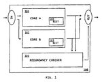
- Fig. 1 shows a graphic illustration of the implementation of two parallel cores utilizing a redundancy checker.
- a first CORE A 101 and a second CORE B 102 are parallel and redundant representations of a logic circuit.
- a REDUNDANCY CHECKER circuit 103 already described, is used to verify the integrity operation of the cores.
- a BIST 104, 105 is shown as part of each of the core structures, but alternately and equally could be shown separately.
- the entire logic circuit structure is within a single FPGA 106 or other logic device. Alternately, the logic circuit could be placed on multiple logic devices.
- the same input is received by CORE A and CORE B and their output is monitored by the REDUNDANCY CHECKER for an exact match.
- the output from the two cores, as well as a failsafe signal from the REDUNDANCY CHECKER are output from the FPGA.
- An output failsafe gate is used, but not shown in Fig. 1 . This feature is described in Fig.
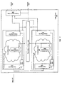
- Fig. 2 shows the implementation of two parallel cores utilizing another embodiment of the redundancy checker.
- Two parallel redundant cores 215, 225 are used to implement the logic circuit. Additional details of the redundant cores are shown which include: input registers 210, 220 , output registers 211, 221 and a built in self test (BIST) feature 214, 224 .
- a redundancy checker 205 is used for reliability and error checking and to activate a fail safe mode 203 .
- a portion of the redundant cores is the critical functions, 212, 222 where the critical states 213, 223 variables or information resides. This information is used for error checking by the redundancy checker 205 as shown.
- Inputs 201 flow into parallel input registers 210, 220 .
- the input is used by the logic circuit according to the system design and the output registers 211, 221 are updated.
- the core output then flows from the output register through the output failsafe gate 204 where it is then combined and becomes output 202 for the system.
- This is a Gate ON communication data output enable. This prevents data from being transmitted when there is a redundancy checker detected failure.
- An output failsafe 203 is activated by the redundancy checker 205 when an error is detected to alert the system.
- the failsafe may be a relay contact closure, an alarm, or a communication of some kind.
- the entire logic circuit 200 resides on a single logic device such as a PAL, CPLD, FPGA, ASIC, or Gate Array. Alternately, the logic circuit could be placed on multiple logic devices.
- Fig. 2 is another embodiment of the redundancy checker that is similar to Fig. 1 .
- the redundancy checker additionally utilizes critical states (i.e. values) within each redundant core for comparison. This additional information is useful for rapidly uncovering unannounced faults.
- the BIST in this case is monitoring the redundant core in the self test.
- Fig. 3 shows another embodiment of the redundancy checker.
- Two parallel redundant cores 315, 325 are used to implement the logic circuit utilizing: input registers 310, 320 , output registers 311, 321 and a built in self test (BIST) feature 314, 324 .
- a redundancy checker 305 is used for reliability and error checking and to activate a fail safe mode 303.
- a portion of the redundant cores is the critical functions, 312, 322 where the critical states 313, 323 variables or information resides. This information is used for error checking by the redundancy checker 305 as shown.
- inputs 301 flow into parallel input registers 310, 320 .
- the input is used by the logic circuit according to the system design and the output registers 311, 321 are updated.
- the core output then flows from the output register through the output failsafe gate 304 where it is then combined and becomes output 302 for the system.
- An output failsafe 303 is activated by the redundancy checker 305 when an error is detected to alert the system.
- the entire logic circuit 300 resides on a single logic device. Alternately, the logic circuit could be placed on multiple logic devices.
- the BIST in this case additionally uses the critical states and output register in the self test.
- Fig. 4 shows important details of a typical built in self test (BIST) 314 .
- BIST built in self test
- Fig. 4 is an additional detail from Fig. 3 .
- Output register values from a redundant core 315 and critical states 313 are input to an output verification routine 401 which passes on to a BIST finite state machine (FSM) 402 .
- the BIST is controlled by the FSM.
- the BIST When activated by an operator, timer, or an event, the BIST will generate input stimuli either as a random sequence or as a programmed sequence 403 to the input register 310 .
- the BIST monitors the redundant core, redundant core output, and critical states to verify correct operation. This verification includes: comparing against a stored reference, comparing against another redundant core, or generating a checksum of the monitored output and verifying this against a reference checksum.
- a typical mission for the logic circuit is to provide a process function between the input and output according to a design.
- the design may be one of readiness, or a safety related function such as in a plant protection system.
- the design may be more involved if it is a process control.
- the logic circuit mission may also include interfacing with control circuits. They include external logic, decision, detection, and control circuits. These circuits are common in process control and safety related plant decisions. They can be binary (on/off) type of circuits, or they may be control related circuits which includes sensors, switches, process controllers, and actuators. They may be part of a relay based system and interface to other computerized systems.
- the redundancy checker is not located on the logic device where the parallel cores are located.
- the redundancy checker is located separately on another logic device. It is then connected by a communication pathway to the outputs of the cores in order to provide redundancy checking.
- the redundancy checker then operates as described in Figs. 1-3 , by providing a fail safe signal, etc.
- the present invention is based on a hardware platform rather than a software-based microprocessor system. It is significantly different than a software based microprocessor control system architecture, by implementing the logic circuit in a logic device thereby eliminating executable software and the problems with software based microprocessor systems, such as software common-mode failures. It provides a highly reliable system suitable for safety critical control systems, including reactor protection systems in nuclear plants.
Claims (3)
- Logikschaltung (200) mit hoher Integrität, welche umfasst:a. eine Vielzahl von parallelen Kernen (215, 225), wobei die parallelen Kerne verwendet werden, um kritische Funktionen der Logikschaltung zu implementieren,b. wobei die parallelen Kerne (215, 225) redundant oder diversitär sind,c. einen Redundanzprüfer (205), wobei der Redundanzprüfer verwendet wird, um:i. zu überprüfen, ob eine Vielzahl von Werten (213) innerhalb eines ersten parallelen Kerns (215) zwischen einem Eingang (201) und einem Ausgang (202) des ersten parallelen Kerns mit einer Vielzahl von Werten (223) innerhalb eines zweiten parallelen Kerns (225) zwischen einem Eingang (201) und einem Ausgang (202) des zweiten parallelen Kerns (225) übereinstimmt, undii. die Logikschaltung (200) in Übereinstimmung mit einem vorbestimmten Kriterium in einen fehlersicheren Zustand (203) zu aktivieren,d. wobei die Logikschaltung (200) mit Schnittstellen zu einer Vielzahl von Eingängen (201) und einer Vielzahl von Ausgängen (202) versehen ist,e. wobei die Logikschaltung eine Aufgabe in Verbindung mit den Eingängen (201) und Ausgängen (202) ausführt, wobei die Aufgabe eine sicherheitskritische Funktion ist,f. wobei die Kommunikation zwischen der Logikschaltung (200) und den Eingängen (201) und den Ausgängen (202) durch zumindest eine Vorkehrung ausgewählt aus der Gruppe bestehend aus:i. Redundanz,ii. zyklische Redundanzprüfung,iii. Toggleprüfung über die Eingänge, undiv. Zurücklesen der Ausgänge,geschützt ist,g. eine integrierte Selbstprüfung (BIST 214, BIST 224), wobei die eingebaute Selbstprüfung verwendet wird, um nicht angezeigte Fehler in irgendeinem der parallelen Kerne offenzulegen,h. wobei die integrierte Selbstprüfung (BIST 214, BIST 224) periodisch oder kontinuierlich durchgeführt wird, während die Logikschaltung (200) die Aufgabe ausführt,i. wobei die kritischen Funktionen (212, 222) der Logikschaltung (200) in zumindest einer Logikvorrichtung (215, 225) implementiert sind, undj. wobei die zumindest eine Logikvorrichtung (215, 125) frei von der Verwendung ausführbarer Software implementiert ist.
- Logikschaltung (200) mit hoher Integrität nach Anspruch 1, wobei der Redundanzprüfer (205) auf einer von den parallelen Kernen (215, 225) separaten Logikvorrichtung angeordnet ist, wobei der Redundanzprüfer mit Ausgängen der parallelen Kerne über einen Kommunikationspfad verbunden ist, oder der Redundanzprüfer auf derselben Logikvorrichtung angeordnet ist, auf der zumindest einer der parallelen Kerne residiert.
- Logikschaltung (200) mit hoher Integrität nach Anspruch 1, wobei die Vielzahl von Werten (213, 223) innerhalb des ersten parallelen Kerns (215) und des zweiten parallelen Kerns (225) Zustandsänderungen in kritischen Funktionen (212, 222) der Logikschaltung sind.
Priority Applications (1)
| Application Number | Priority Date | Filing Date | Title |
|---|---|---|---|
| EP11004699.2A EP2533154B1 (de) | 2011-06-09 | 2011-06-09 | Fehlererfassung und -minderung in logischen Schaltungen |
Applications Claiming Priority (1)
| Application Number | Priority Date | Filing Date | Title |
|---|---|---|---|
| EP11004699.2A EP2533154B1 (de) | 2011-06-09 | 2011-06-09 | Fehlererfassung und -minderung in logischen Schaltungen |
Publications (3)
| Publication Number | Publication Date |
|---|---|
| EP2533154A2 EP2533154A2 (de) | 2012-12-12 |
| EP2533154A3 EP2533154A3 (de) | 2014-05-28 |
| EP2533154B1 true EP2533154B1 (de) | 2015-08-12 |
Family
ID=44772634
Family Applications (1)
| Application Number | Title | Priority Date | Filing Date |
|---|---|---|---|
| EP11004699.2A Not-in-force EP2533154B1 (de) | 2011-06-09 | 2011-06-09 | Fehlererfassung und -minderung in logischen Schaltungen |
Country Status (1)
| Country | Link |
|---|---|
| EP (1) | EP2533154B1 (de) |
Cited By (1)
| Publication number | Priority date | Publication date | Assignee | Title |
|---|---|---|---|---|
| US11157673B2 (en) | 2019-07-12 | 2021-10-26 | Ratier-Figeac Sas | Field programmable gate array (FPGA) having dissimilar cores |
Families Citing this family (6)
| Publication number | Priority date | Publication date | Assignee | Title |
|---|---|---|---|---|
| EP2958022B1 (de) * | 2013-04-24 | 2017-02-01 | ALSTOM Transport Technologies | Inhärente ausfallsichere einheit zur steuerungs- und befehlsaktivierung mit 2-aus-2-architektur |
| DE102013211422A1 (de) * | 2013-06-18 | 2014-12-18 | Kuka Laboratories Gmbh | Steuervorrichtung einer Maschine und Maschine mit einer Steuervorrichtung |
| CN108182167B (zh) * | 2017-12-19 | 2021-09-28 | 深圳市航天新源科技有限公司 | 基于集成电路的可重构架构及实现方法 |
| CN110955218B (zh) * | 2018-09-26 | 2021-03-23 | 中国船舶重工集团公司第七一九研究所 | 一种核动力装置主、备控制系统的冗余监控电路 |
| US11378934B2 (en) * | 2019-09-09 | 2022-07-05 | Baker Hughes Oilfield Operations Llc | Shadow function for protection monitoring systems |
| DE102020104595B3 (de) * | 2020-02-21 | 2021-05-12 | Infineon Technologies Ag | Integrierter Schaltkreis mit Selbsttestschaltung, Verfahren zum Betreiben eines integrierten Schaltkreises mit Selbsttestschaltung, Mehrkernprozessoreinrichtung und Verfahren zum Betreiben einer Mehrkernprozessoreinrichtung |
Family Cites Families (8)
| Publication number | Priority date | Publication date | Assignee | Title |
|---|---|---|---|---|
| JPH061402B2 (ja) * | 1987-03-20 | 1994-01-05 | 住友電気工業株式会社 | 多重系制御回路 |
| US5144230A (en) * | 1990-11-26 | 1992-09-01 | The Boeing Company | Method and system for testing integrated circuits by cycle stealing |
| US5574849A (en) | 1992-12-17 | 1996-11-12 | Tandem Computers Incorporated | Synchronized data transmission between elements of a processing system |
| JP3412349B2 (ja) * | 1994-12-28 | 2003-06-03 | 株式会社日立製作所 | 制御装置 |
| US7134104B2 (en) | 2003-12-05 | 2006-11-07 | International Business Machines Corporation | Method of selectively building redundant logic structures to improve fault tolerance |
| US7290169B2 (en) | 2004-04-06 | 2007-10-30 | Hewlett-Packard Development Company, L.P. | Core-level processor lockstepping |
| US7237144B2 (en) | 2004-04-06 | 2007-06-26 | Hewlett-Packard Development Company, L.P. | Off-chip lockstep checking |
| US7747932B2 (en) | 2005-06-30 | 2010-06-29 | Intel Corporation | Reducing the uncorrectable error rate in a lockstepped dual-modular redundancy system |
-
2011
- 2011-06-09 EP EP11004699.2A patent/EP2533154B1/de not_active Not-in-force
Cited By (1)
| Publication number | Priority date | Publication date | Assignee | Title |
|---|---|---|---|---|
| US11157673B2 (en) | 2019-07-12 | 2021-10-26 | Ratier-Figeac Sas | Field programmable gate array (FPGA) having dissimilar cores |
Also Published As
| Publication number | Publication date |
|---|---|
| EP2533154A2 (de) | 2012-12-12 |
| EP2533154A3 (de) | 2014-05-28 |
Similar Documents
| Publication | Publication Date | Title |
|---|---|---|
| US8117512B2 (en) | Failure detection and mitigation in logic circuits | |
| EP2533154B1 (de) | Fehlererfassung und -minderung in logischen Schaltungen | |
| US7877627B1 (en) | Multiple redundant computer system combining fault diagnostics and majority voting with dissimilar redundancy technology | |
| CN102841828B (zh) | 逻辑电路中的故障检测和减轻 | |
| Avižienis | Design of fault-tolerant computers | |
| US20180211734A1 (en) | Reactor protection-processor-to-reactor-trip breaker interface and method for operating the same | |
| CN109213118B (zh) | 具有用于飞机的三重冗余的控制系统及用于管理它的方法 | |
| US10078565B1 (en) | Error recovery for redundant processing circuits | |
| US6367031B1 (en) | Critical control adaption of integrated modular architecture | |
| US20120030524A1 (en) | High reliability method of data processing, and controller unit | |
| KR101825568B1 (ko) | 논리 회로에서의 고장 검출 및 완화 | |
| Kastil et al. | Dependability analysis of fault tolerant systems based on partial dynamic reconfiguration implemented into FPGA | |
| Wang et al. | The reliability and availability analysis of SEU mitigation techniques in SRAM-based FPGAs | |
| Sharma | Fault tolerant techniques for reconfigurable platforms | |
| Agarwal et al. | State model for scheduling Built-in Self-Test and scrubbing in FPGA to maximize the system availability in space applications | |
| Lubaszewski et al. | Reliable fail-safe systems | |
| Ilayaranimangammal et al. | Exposure and expulsion the soft errors in digital systems using redundancy techniques | |
| Bennetts | Designing reliable computer systems. The fault-tolerant approach-1 | |
| Nithya et al. | Very large scale integrated solution for stuck at faults in synchronous sequential circuits | |
| Chizek | Programmable Logic Device (PLD) Safety Design Approach | |
| Patooghy et al. | A solution to single point of failure using voter replication and disagreement detection | |
| Kershaw | Dependable systems using'VIPER' | |
| Gericota et al. | Robust configurable system design with built-in self-healing | |
| Halbert | Selfchecking computer module based on the Viper microprocessor | |
| Khairullah et al. | Realization of Dependable Digital Systems for Safety-Critical Computer Systems using FPGAs |
Legal Events
| Date | Code | Title | Description |
|---|---|---|---|
| PUAI | Public reference made under article 153(3) epc to a published international application that has entered the european phase |
Free format text: ORIGINAL CODE: 0009012 |
|
| AK | Designated contracting states |
Kind code of ref document: A2 Designated state(s): AL AT BE BG CH CY CZ DE DK EE ES FI FR GB GR HR HU IE IS IT LI LT LU LV MC MK MT NL NO PL PT RO RS SE SI SK SM TR |
|
| AX | Request for extension of the european patent |
Extension state: BA ME |
|
| PUAL | Search report despatched |
Free format text: ORIGINAL CODE: 0009013 |
|
| AK | Designated contracting states |
Kind code of ref document: A3 Designated state(s): AL AT BE BG CH CY CZ DE DK EE ES FI FR GB GR HR HU IE IS IT LI LT LU LV MC MK MT NL NO PL PT RO RS SE SI SK SM TR |
|
| AX | Request for extension of the european patent |
Extension state: BA ME |
|
| RIC1 | Information provided on ipc code assigned before grant |
Ipc: G06F 11/27 20060101ALI20140423BHEP Ipc: G06F 11/22 20060101ALI20140423BHEP Ipc: G06F 11/16 20060101AFI20140423BHEP Ipc: G06F 11/07 20060101ALI20140423BHEP |
|
| 17P | Request for examination filed |
Effective date: 20141017 |
|
| RBV | Designated contracting states (corrected) |
Designated state(s): AL AT BE BG CH CY CZ DE DK EE ES FI FR GB GR HR HU IE IS IT LI LT LU LV MC MK MT NL NO PL PT RO RS SE SI SK SM TR |
|
| 17Q | First examination report despatched |
Effective date: 20141120 |
|
| GRAP | Despatch of communication of intention to grant a patent |
Free format text: ORIGINAL CODE: EPIDOSNIGR1 |
|
| GRAS | Grant fee paid |
Free format text: ORIGINAL CODE: EPIDOSNIGR3 |
|
| GRAA | (expected) grant |
Free format text: ORIGINAL CODE: 0009210 |
|
| INTG | Intention to grant announced |
Effective date: 20150615 |
|
| AK | Designated contracting states |
Kind code of ref document: B1 Designated state(s): AL AT BE BG CH CY CZ DE DK EE ES FI FR GB GR HR HU IE IS IT LI LT LU LV MC MK MT NL NO PL PT RO RS SE SI SK SM TR |
|
| REG | Reference to a national code |
Ref country code: GB Ref legal event code: FG4D |
|
| REG | Reference to a national code |
Ref country code: CH Ref legal event code: EP |
|
| REG | Reference to a national code |
Ref country code: AT Ref legal event code: REF Ref document number: 742702 Country of ref document: AT Kind code of ref document: T Effective date: 20150815 |
|
| REG | Reference to a national code |
Ref country code: IE Ref legal event code: FG4D |
|
| REG | Reference to a national code |
Ref country code: DE Ref legal event code: R096 Ref document number: 602011018581 Country of ref document: DE |
|
| REG | Reference to a national code |
Ref country code: CH Ref legal event code: NV Representative=s name: BOHEST AG, CH |
|
| REG | Reference to a national code |
Ref country code: SE Ref legal event code: TRGR |
|
| REG | Reference to a national code |
Ref country code: LT Ref legal event code: MG4D |
|
| REG | Reference to a national code |
Ref country code: AT Ref legal event code: MK05 Ref document number: 742702 Country of ref document: AT Kind code of ref document: T Effective date: 20150812 |
|
| REG | Reference to a national code |
Ref country code: NL Ref legal event code: MP Effective date: 20150812 |
|
| PG25 | Lapsed in a contracting state [announced via postgrant information from national office to epo] |
Ref country code: FI Free format text: LAPSE BECAUSE OF FAILURE TO SUBMIT A TRANSLATION OF THE DESCRIPTION OR TO PAY THE FEE WITHIN THE PRESCRIBED TIME-LIMIT Effective date: 20150812 Ref country code: LV Free format text: LAPSE BECAUSE OF FAILURE TO SUBMIT A TRANSLATION OF THE DESCRIPTION OR TO PAY THE FEE WITHIN THE PRESCRIBED TIME-LIMIT Effective date: 20150812 Ref country code: LT Free format text: LAPSE BECAUSE OF FAILURE TO SUBMIT A TRANSLATION OF THE DESCRIPTION OR TO PAY THE FEE WITHIN THE PRESCRIBED TIME-LIMIT Effective date: 20150812 Ref country code: NO Free format text: LAPSE BECAUSE OF FAILURE TO SUBMIT A TRANSLATION OF THE DESCRIPTION OR TO PAY THE FEE WITHIN THE PRESCRIBED TIME-LIMIT Effective date: 20151112 Ref country code: GR Free format text: LAPSE BECAUSE OF FAILURE TO SUBMIT A TRANSLATION OF THE DESCRIPTION OR TO PAY THE FEE WITHIN THE PRESCRIBED TIME-LIMIT Effective date: 20151113 |
|
| PG25 | Lapsed in a contracting state [announced via postgrant information from national office to epo] |
Ref country code: PL Free format text: LAPSE BECAUSE OF FAILURE TO SUBMIT A TRANSLATION OF THE DESCRIPTION OR TO PAY THE FEE WITHIN THE PRESCRIBED TIME-LIMIT Effective date: 20150812 Ref country code: RS Free format text: LAPSE BECAUSE OF FAILURE TO SUBMIT A TRANSLATION OF THE DESCRIPTION OR TO PAY THE FEE WITHIN THE PRESCRIBED TIME-LIMIT Effective date: 20150812 Ref country code: ES Free format text: LAPSE BECAUSE OF FAILURE TO SUBMIT A TRANSLATION OF THE DESCRIPTION OR TO PAY THE FEE WITHIN THE PRESCRIBED TIME-LIMIT Effective date: 20150812 Ref country code: AT Free format text: LAPSE BECAUSE OF FAILURE TO SUBMIT A TRANSLATION OF THE DESCRIPTION OR TO PAY THE FEE WITHIN THE PRESCRIBED TIME-LIMIT Effective date: 20150812 Ref country code: IS Free format text: LAPSE BECAUSE OF FAILURE TO SUBMIT A TRANSLATION OF THE DESCRIPTION OR TO PAY THE FEE WITHIN THE PRESCRIBED TIME-LIMIT Effective date: 20151212 Ref country code: PT Free format text: LAPSE BECAUSE OF FAILURE TO SUBMIT A TRANSLATION OF THE DESCRIPTION OR TO PAY THE FEE WITHIN THE PRESCRIBED TIME-LIMIT Effective date: 20151214 Ref country code: HR Free format text: LAPSE BECAUSE OF FAILURE TO SUBMIT A TRANSLATION OF THE DESCRIPTION OR TO PAY THE FEE WITHIN THE PRESCRIBED TIME-LIMIT Effective date: 20150812 |
|
| PG25 | Lapsed in a contracting state [announced via postgrant information from national office to epo] |
Ref country code: NL Free format text: LAPSE BECAUSE OF FAILURE TO SUBMIT A TRANSLATION OF THE DESCRIPTION OR TO PAY THE FEE WITHIN THE PRESCRIBED TIME-LIMIT Effective date: 20150812 |
|
| PG25 | Lapsed in a contracting state [announced via postgrant information from national office to epo] |
Ref country code: IT Free format text: LAPSE BECAUSE OF FAILURE TO SUBMIT A TRANSLATION OF THE DESCRIPTION OR TO PAY THE FEE WITHIN THE PRESCRIBED TIME-LIMIT Effective date: 20150812 Ref country code: EE Free format text: LAPSE BECAUSE OF FAILURE TO SUBMIT A TRANSLATION OF THE DESCRIPTION OR TO PAY THE FEE WITHIN THE PRESCRIBED TIME-LIMIT Effective date: 20150812 Ref country code: SK Free format text: LAPSE BECAUSE OF FAILURE TO SUBMIT A TRANSLATION OF THE DESCRIPTION OR TO PAY THE FEE WITHIN THE PRESCRIBED TIME-LIMIT Effective date: 20150812 Ref country code: DK Free format text: LAPSE BECAUSE OF FAILURE TO SUBMIT A TRANSLATION OF THE DESCRIPTION OR TO PAY THE FEE WITHIN THE PRESCRIBED TIME-LIMIT Effective date: 20150812 |
|
| REG | Reference to a national code |
Ref country code: DE Ref legal event code: R097 Ref document number: 602011018581 Country of ref document: DE |
|
| PG25 | Lapsed in a contracting state [announced via postgrant information from national office to epo] |
Ref country code: RO Free format text: LAPSE BECAUSE OF FAILURE TO SUBMIT A TRANSLATION OF THE DESCRIPTION OR TO PAY THE FEE WITHIN THE PRESCRIBED TIME-LIMIT Effective date: 20150812 |
|
| REG | Reference to a national code |
Ref country code: FR Ref legal event code: PLFP Year of fee payment: 6 |
|
| PLBE | No opposition filed within time limit |
Free format text: ORIGINAL CODE: 0009261 |
|
| STAA | Information on the status of an ep patent application or granted ep patent |
Free format text: STATUS: NO OPPOSITION FILED WITHIN TIME LIMIT |
|
| 26N | No opposition filed |
Effective date: 20160513 |
|
| PG25 | Lapsed in a contracting state [announced via postgrant information from national office to epo] |
Ref country code: SI Free format text: LAPSE BECAUSE OF FAILURE TO SUBMIT A TRANSLATION OF THE DESCRIPTION OR TO PAY THE FEE WITHIN THE PRESCRIBED TIME-LIMIT Effective date: 20150812 |
|
| REG | Reference to a national code |
Ref country code: DE Ref legal event code: R119 Ref document number: 602011018581 Country of ref document: DE |
|
| PG25 | Lapsed in a contracting state [announced via postgrant information from national office to epo] |
Ref country code: MC Free format text: LAPSE BECAUSE OF FAILURE TO SUBMIT A TRANSLATION OF THE DESCRIPTION OR TO PAY THE FEE WITHIN THE PRESCRIBED TIME-LIMIT Effective date: 20150812 |
|
| REG | Reference to a national code |
Ref country code: IE Ref legal event code: MM4A |
|
| PG25 | Lapsed in a contracting state [announced via postgrant information from national office to epo] |
Ref country code: DE Free format text: LAPSE BECAUSE OF NON-PAYMENT OF DUE FEES Effective date: 20170103 |
|
| REG | Reference to a national code |
Ref country code: FR Ref legal event code: PLFP Year of fee payment: 7 |
|
| PG25 | Lapsed in a contracting state [announced via postgrant information from national office to epo] |
Ref country code: IE Free format text: LAPSE BECAUSE OF NON-PAYMENT OF DUE FEES Effective date: 20160609 |
|
| REG | Reference to a national code |
Ref country code: FR Ref legal event code: PLFP Year of fee payment: 8 |
|
| PG25 | Lapsed in a contracting state [announced via postgrant information from national office to epo] |
Ref country code: SM Free format text: LAPSE BECAUSE OF FAILURE TO SUBMIT A TRANSLATION OF THE DESCRIPTION OR TO PAY THE FEE WITHIN THE PRESCRIBED TIME-LIMIT Effective date: 20150812 Ref country code: CY Free format text: LAPSE BECAUSE OF FAILURE TO SUBMIT A TRANSLATION OF THE DESCRIPTION OR TO PAY THE FEE WITHIN THE PRESCRIBED TIME-LIMIT Effective date: 20150812 Ref country code: HU Free format text: LAPSE BECAUSE OF FAILURE TO SUBMIT A TRANSLATION OF THE DESCRIPTION OR TO PAY THE FEE WITHIN THE PRESCRIBED TIME-LIMIT; INVALID AB INITIO Effective date: 20110609 |
|
| PG25 | Lapsed in a contracting state [announced via postgrant information from national office to epo] |
Ref country code: MK Free format text: LAPSE BECAUSE OF FAILURE TO SUBMIT A TRANSLATION OF THE DESCRIPTION OR TO PAY THE FEE WITHIN THE PRESCRIBED TIME-LIMIT Effective date: 20150812 Ref country code: MT Free format text: LAPSE BECAUSE OF NON-PAYMENT OF DUE FEES Effective date: 20160630 Ref country code: LU Free format text: LAPSE BECAUSE OF NON-PAYMENT OF DUE FEES Effective date: 20160609 Ref country code: TR Free format text: LAPSE BECAUSE OF FAILURE TO SUBMIT A TRANSLATION OF THE DESCRIPTION OR TO PAY THE FEE WITHIN THE PRESCRIBED TIME-LIMIT Effective date: 20150812 |
|
| PG25 | Lapsed in a contracting state [announced via postgrant information from national office to epo] |
Ref country code: BG Free format text: LAPSE BECAUSE OF FAILURE TO SUBMIT A TRANSLATION OF THE DESCRIPTION OR TO PAY THE FEE WITHIN THE PRESCRIBED TIME-LIMIT Effective date: 20150812 |
|
| PG25 | Lapsed in a contracting state [announced via postgrant information from national office to epo] |
Ref country code: AL Free format text: LAPSE BECAUSE OF FAILURE TO SUBMIT A TRANSLATION OF THE DESCRIPTION OR TO PAY THE FEE WITHIN THE PRESCRIBED TIME-LIMIT Effective date: 20150812 |
|
| PGFP | Annual fee paid to national office [announced via postgrant information from national office to epo] |
Ref country code: CZ Payment date: 20210609 Year of fee payment: 11 Ref country code: FR Payment date: 20210628 Year of fee payment: 11 |
|
| PGFP | Annual fee paid to national office [announced via postgrant information from national office to epo] |
Ref country code: SE Payment date: 20210628 Year of fee payment: 11 Ref country code: BE Payment date: 20210625 Year of fee payment: 11 Ref country code: GB Payment date: 20210625 Year of fee payment: 11 Ref country code: CH Payment date: 20210628 Year of fee payment: 11 |
|
| PG25 | Lapsed in a contracting state [announced via postgrant information from national office to epo] |
Ref country code: CZ Free format text: LAPSE BECAUSE OF NON-PAYMENT OF DUE FEES Effective date: 20220609 |
|
| REG | Reference to a national code |
Ref country code: CH Ref legal event code: PL Ref country code: SE Ref legal event code: EUG |
|
| REG | Reference to a national code |
Ref country code: BE Ref legal event code: MM Effective date: 20220630 |
|
| GBPC | Gb: european patent ceased through non-payment of renewal fee |
Effective date: 20220609 |
|
| PG25 | Lapsed in a contracting state [announced via postgrant information from national office to epo] |
Ref country code: SE Free format text: LAPSE BECAUSE OF NON-PAYMENT OF DUE FEES Effective date: 20220610 Ref country code: LI Free format text: LAPSE BECAUSE OF NON-PAYMENT OF DUE FEES Effective date: 20220630 Ref country code: FR Free format text: LAPSE BECAUSE OF NON-PAYMENT OF DUE FEES Effective date: 20220630 Ref country code: CH Free format text: LAPSE BECAUSE OF NON-PAYMENT OF DUE FEES Effective date: 20220630 |
|
| PG25 | Lapsed in a contracting state [announced via postgrant information from national office to epo] |
Ref country code: GB Free format text: LAPSE BECAUSE OF NON-PAYMENT OF DUE FEES Effective date: 20220609 Ref country code: BE Free format text: LAPSE BECAUSE OF NON-PAYMENT OF DUE FEES Effective date: 20220630 |