EP2528117A1 - Group iii nitride semiconductor element - Google Patents
Group iii nitride semiconductor element Download PDFInfo
- Publication number
- EP2528117A1 EP2528117A1 EP10843086A EP10843086A EP2528117A1 EP 2528117 A1 EP2528117 A1 EP 2528117A1 EP 10843086 A EP10843086 A EP 10843086A EP 10843086 A EP10843086 A EP 10843086A EP 2528117 A1 EP2528117 A1 EP 2528117A1
- Authority
- EP
- European Patent Office
- Prior art keywords
- group iii
- iii nitride
- electrode
- semiconductor region
- nitride semiconductor
- Prior art date
- Legal status (The legal status is an assumption and is not a legal conclusion. Google has not performed a legal analysis and makes no representation as to the accuracy of the status listed.)
- Withdrawn
Links
Images






Classifications
-
- H—ELECTRICITY
- H10—SEMICONDUCTOR DEVICES; ELECTRIC SOLID-STATE DEVICES NOT OTHERWISE PROVIDED FOR
- H10H—INORGANIC LIGHT-EMITTING SEMICONDUCTOR DEVICES HAVING POTENTIAL BARRIERS
- H10H20/00—Individual inorganic light-emitting semiconductor devices having potential barriers, e.g. light-emitting diodes [LED]
- H10H20/80—Constructional details
- H10H20/81—Bodies
- H10H20/817—Bodies characterised by the crystal structures or orientations, e.g. polycrystalline, amorphous or porous
-
- H—ELECTRICITY
- H10—SEMICONDUCTOR DEVICES; ELECTRIC SOLID-STATE DEVICES NOT OTHERWISE PROVIDED FOR
- H10D—INORGANIC ELECTRIC SEMICONDUCTOR DEVICES
- H10D64/00—Electrodes of devices having potential barriers
- H10D64/01—Manufacture or treatment
- H10D64/011—Manufacture or treatment of electrodes ohmically coupled to a semiconductor
- H10D64/0116—Manufacture or treatment of electrodes ohmically coupled to a semiconductor to Group III-V semiconductors
-
- H—ELECTRICITY
- H10—SEMICONDUCTOR DEVICES; ELECTRIC SOLID-STATE DEVICES NOT OTHERWISE PROVIDED FOR
- H10D—INORGANIC ELECTRIC SEMICONDUCTOR DEVICES
- H10D62/00—Semiconductor bodies, or regions thereof, of devices having potential barriers
- H10D62/40—Crystalline structures
- H10D62/405—Orientations of crystalline planes
-
- H—ELECTRICITY
- H10—SEMICONDUCTOR DEVICES; ELECTRIC SOLID-STATE DEVICES NOT OTHERWISE PROVIDED FOR
- H10D—INORGANIC ELECTRIC SEMICONDUCTOR DEVICES
- H10D62/00—Semiconductor bodies, or regions thereof, of devices having potential barriers
- H10D62/80—Semiconductor bodies, or regions thereof, of devices having potential barriers characterised by the materials
- H10D62/85—Semiconductor bodies, or regions thereof, of devices having potential barriers characterised by the materials being Group III-V materials, e.g. GaAs
-
- H—ELECTRICITY
- H10—SEMICONDUCTOR DEVICES; ELECTRIC SOLID-STATE DEVICES NOT OTHERWISE PROVIDED FOR
- H10D—INORGANIC ELECTRIC SEMICONDUCTOR DEVICES
- H10D64/00—Electrodes of devices having potential barriers
- H10D64/60—Electrodes characterised by their materials
- H10D64/62—Electrodes ohmically coupled to a semiconductor
-
- H—ELECTRICITY
- H10—SEMICONDUCTOR DEVICES; ELECTRIC SOLID-STATE DEVICES NOT OTHERWISE PROVIDED FOR
- H10H—INORGANIC LIGHT-EMITTING SEMICONDUCTOR DEVICES HAVING POTENTIAL BARRIERS
- H10H20/00—Individual inorganic light-emitting semiconductor devices having potential barriers, e.g. light-emitting diodes [LED]
- H10H20/80—Constructional details
- H10H20/83—Electrodes
-
- H—ELECTRICITY
- H10—SEMICONDUCTOR DEVICES; ELECTRIC SOLID-STATE DEVICES NOT OTHERWISE PROVIDED FOR
- H10D—INORGANIC ELECTRIC SEMICONDUCTOR DEVICES
- H10D62/00—Semiconductor bodies, or regions thereof, of devices having potential barriers
- H10D62/80—Semiconductor bodies, or regions thereof, of devices having potential barriers characterised by the materials
- H10D62/85—Semiconductor bodies, or regions thereof, of devices having potential barriers characterised by the materials being Group III-V materials, e.g. GaAs
- H10D62/8503—Nitride Group III-V materials, e.g. AlN or GaN
-
- H—ELECTRICITY
- H10—SEMICONDUCTOR DEVICES; ELECTRIC SOLID-STATE DEVICES NOT OTHERWISE PROVIDED FOR
- H10H—INORGANIC LIGHT-EMITTING SEMICONDUCTOR DEVICES HAVING POTENTIAL BARRIERS
- H10H20/00—Individual inorganic light-emitting semiconductor devices having potential barriers, e.g. light-emitting diodes [LED]
- H10H20/80—Constructional details
- H10H20/81—Bodies
- H10H20/822—Materials of the light-emitting regions
- H10H20/824—Materials of the light-emitting regions comprising only Group III-V materials, e.g. GaP
- H10H20/825—Materials of the light-emitting regions comprising only Group III-V materials, e.g. GaP containing nitrogen, e.g. GaN
-
- H—ELECTRICITY
- H10—SEMICONDUCTOR DEVICES; ELECTRIC SOLID-STATE DEVICES NOT OTHERWISE PROVIDED FOR
- H10H—INORGANIC LIGHT-EMITTING SEMICONDUCTOR DEVICES HAVING POTENTIAL BARRIERS
- H10H20/00—Individual inorganic light-emitting semiconductor devices having potential barriers, e.g. light-emitting diodes [LED]
- H10H20/80—Constructional details
- H10H20/83—Electrodes
- H10H20/832—Electrodes characterised by their material
Definitions
- the present invention relates to a Group III nitride semiconductor device.
- Patent Literatures 1 and 2 describe a method for forming an ohmic electrode on a p-type gallium nitride (GaN) layer grown on a (0001) plane or c-plane.
- Ni/Au film is evaporated onto the p-type GaN layer and thereafter a thermal treatment is carried out in an oxygen atmosphere.
- An oxide film exists on the surface of the p-type GaN layer, but nickel absorbs the oxide film by this method. Then nickel binds to oxygen atoms of the oxide film, thereby removing the oxide film. This allows gold to come into contact with the p-type GaN crystal, thereby forming an ohmic contact.
- Patent Literature 3 describes the result of an experiment.
- a p-type Group III nitride semiconductor layer is grown on a sapphire substrate. Then the substrate is heated to 300°C and thereafter platinum or nickel is evaporated onto a surface of the Group III nitride semiconductor layer. Thereafter, the contact resistance is measured.
- Patent Literature 4 platinum is evaporated onto a p-type GaN contact layer. Then a thermal treatment is carried out in the range of 500°C to 600°C in an oxygen atmosphere to form an alloy electrode.
- Group III nitride-based semiconductor light emitting devices depending upon the emission wavelength required, there are cases where a Group III nitride semiconductor containing indium, e.g., InGaN or InAlGaN, is grown on a Group III nitride semiconductor substrate, e.g., a GaN substrate. Since the diameter of indium atom is larger than the diameter of gallium atom, increase in the indium composition leads to increase in internal strain in the indium-containing layer because of lattice mismatch. As a result, a large piezoelectric field is induced in the layer, so as to decrease the recombination probability and thus reduce the luminous efficiency.
- a Group III nitride semiconductor containing indium e.g., InGaN or InAlGaN
- a technology to solve this problem is to grow the indium-containing Group III nitride semiconductor on a plane largely inclined from the c-plane of the Group III nitride semiconductor crystal. The reason is that the piezoelectric field in the layer can be reduced by growing the indium-containing Group III nitride semiconductor on the plane largely inclined from the c-plane.
- the contact resistance decreases when the electrode is formed on the primary surface of Group III nitride semiconductor parallel to the c-plane.
- the contact resistance increases when the electrode is formed on the primary surface of the Group III nitride semiconductor largely inclined from the c-plane. It is because a thick surface oxide film is formed when the primary surface of the Group III nitride semiconductor is largely inclined from the c-plane.
- the present invention provides the group III nitride semiconductor device that can reduce the contact resistance between the Group III nitride semiconductor and an electrode on the Group III nitride semiconductor when a surface of the Group III nitride semiconductor is inclined from the c-plane.
- a group III nitride semiconductor device comprises (1) a semiconductor region having a surface comprised of a Group III nitride crystal, the semiconductor region being doped with a p-type dopant, the surface being one of a semipolar surface and a nonpolar surface, (2) a metal electrode provided on the surface, and (3) a transition layer formed between the Group III nitride crystal of the semiconductor region and the metal electrode, the transition layer being made by interdiffusion of a metal of the metal electrode and a Group III nitride of the semiconductor region.
- the surface of the Group III nitride semiconductor is nonpolar or semipolar, the Group III nitride crystal and the metal are likely to bind to each other on the surface.
- the transition layer is generated in between the semiconductor region and the electrode in the result, unlike the case of forming the electrode on the c-plane of the semiconductor region.
- the transition layer results from interdiffusion between the metal electrode and the Group III nitride crystal of the semiconductor region.
- the transition layer improves adhesion between the semiconductor region and the metal electrode, so as to decrease the contact resistance between them.
- a thickness of the transition layer may be more than or equal to 0.5 nm, and less than or equal to 3 nm. The contact resistance can be more effectively reduced by the transition layer in such thickness.
- the metal electrode may contain at least one of palladium and platinum.
- the transition layer is suitably made between the metal electrode and the semiconductor region by such metal electrode.
- the metal electrode may be completed without a thermal treatment process after forming a metal film on the surface.
- the transition layer is suitably made between the electrode and the semiconductor region by such electrode.
- An angle between a normal to the surface and a c-axis of the Group III nitride crystal constituting the semiconductor region may be in the range of 10 degrees to 80 degrees or the range of 100 degrees to 170 degrees.
- the semipolar surface of the semiconductor region can be provided hereby.
- An angle between a normal to the surface and a c-axis of the Group III nitride crystal constituting the semiconductor region may be in the range of 63 degrees to 80 degrees or the range of 100 degrees to 117 degrees.
- the semipolar surface of the semiconductor region can be provided hereby.
- the Group III nitride semiconductor device where the contact resistance between the semiconductor region and the electrode on the semiconductor region can be reduced, can be provided, when the Group III nitride semiconductor region has the surface inclined from the c-plane.
- Fig. 1 is a drawing showing major steps in a method for fabricating a Group III nitride semiconductor device according to an embodiment.
- Figs. 2 and 3 are drawings schematically showing products in the major steps shown in Fig. 1 .
- the Group III nitride semiconductor device is an optical device, for example, such as a laser diode and a light emitting diode, or an electronic device, for example, such as a pn junction diode and a transistor.
- Step S101 in Fig. 1 is to prepare a substrate 11 shown in Part (a) of Fig. 2 .
- the substrate 11 has a nonpolar or semipolar primary surface.
- the substrate 11 is comprised, for example, of Group III nitride semiconductor of the wurtzite structure.
- Group III nitride semiconductors include AlN, gallium nitride-based semiconductors such as AlGaN and GaN, and so on. With use of these GaN-based semiconductors, the primary surface 11a of the substrate 11 has nonpolar or semipolar nature.
- a normal vector NV is normal to the primary surface 11a of the substrate 11.
- An angle Alpha between the normal vector NV on the substrate 11 and the c-axis vector VC is, for example, in the range of not less than 10 degrees and not more than 170 degrees.
- step S102 the substrate 11 is placed in a processing device 10a such as a growth furnace, as shown in Part (b) of Fig. 2 . Thereafter, a semiconductor region 13 is grown on the primary surface 11a of the substrate 11.
- the semiconductor region 13 is comprised of Group III nitride crystal.
- the semiconductor region 13 preferably includes, for example, a GaN-based semiconductor layer or a plurality of GaN-based semiconductor layers.
- the semiconductor region 13 is provided by epitaxial growth on the primary surface 11a of the substrate 11. This crystal growth is carried out, for example, by organometallic vapor phase epitaxy or by molecular beam epitaxy.
- a top surface 13a of the semiconductor region 13 has nonpolar or semipolar nature.
- the surface 13a of the semiconductor region 13 is comprised of p-type Group III nitride semiconductor, e.g., GaN-based semiconductor.
- the p-type Group III nitride semiconductor is doped with a high concentration of a p-type dopant, e.g., Mg. It should be noted that the formation of the p-type Group III nitride semiconductor is not limited only to the epitaxial growth. These steps result in producing a first substrate product P1.
- Step S103 is to take the first substrate product P1 out of the processing device 10a.
- the surface 13a of the semiconductor region 13 exposed to the atmosphere is more likely to be oxidized than a polar surface as the c-plane.
- a relatively thick native oxide film is formed on the nonpolar or semipolar surface of the semiconductor region 13 exposed to the atmosphere.
- the native oxide film is formed during transportation of the substrate product P1 from the processing device 10a to a film-forming device. As shown in Part (c) of Fig. 2 , an oxidized product 15 of the native oxide film exists on the surface of the first substrate product P1.
- a step to perform a pretreatment of the first substrate product P1 may be optionally provided as step S104. It is preferable to use, for example, at least one of aqua regia, hydrofluoric acid, and hydrochloric acid as a solution for the pretreatment. The pretreatment using these solutions can remove the oxidized product 15 formed on the surface 13a of the semiconductor region 13, to some extent.
- step S105 is carried out to place the first substrate product P1 in the film-forming device 10b, as shown in Part (a) of Fig. 3 .
- a mask for a lift-off procedure can be formed on the first substrate product P1, prior to the placement thereof in the film-forming device 10b.
- This mask includes a resist layer.
- the film-forming device 10b is vacuumized down to the vacuum degree of about 1 ⁇ 10 -6 Torr. It is noted that 1 Pa is equivalent to 0.0075 Torr.
- step S 106 is to deposit a film of metal electrode 17 on the surface of the first substrate product P1, using the film-forming device 10b.
- the metal electrode 17 can be formed, for example, by electron beam evaporation or by resistive heating.
- the temperature of the substrate 11 at this time is preferably, for example, not less than 15 degrees and not more than 100 degrees.
- the metal electrode 17 contains Pd.
- the metal electrode 17 is comprised of a Pd layer.
- the thickness of the Pd layer is preferably, for example, more than or equal to 10 nm.
- a transition layer 19 is made at an interface between the metal electrode 17 and the surface 13a of the semiconductor region 13.
- the transition layer 19 is a layer resulting from interdiffusion of Pd and GaN.
- the transition layer 19 is made at the same time as the deposition of the metal electrode 17.
- the surface 13a of the semiconductor region 13 is nonpolar or semipolar, it is likely to bind to metal, different from the c-plane, and thus such transition layer 19 spreads.
- the formation of the metal electrode 17 results in forming an ohmic electrode in electric contact with the surface 13a of the semiconductor region 13. This step results in producing a second substrate product P2.
- the substrate product P2 includes the metal electrode 17 provided on the semiconductor region 13 of the substrate product P1, and the transition layer 19 made at the interface between the semiconductor region 13 and the metal electrode 17.
- Step S107 is to take the second substrate product P2 out of the film-forming device 10b. If the mask for the lift-off procedure is formed on the first substrate product P1, a step to perform the lift-off procedure is carried out to form a patterned electrode.
- the lift-off procedure is carried out, for example, using acetone or the like.
- the present embodiment does not involve such a thermal treatment to complete the formation of the ohmic electrode. Then the second substrate product P2 is cut in a chip form. This completes the Group III nitride semiconductor device.
- Patent Literatures 1 and 2 The inventors attempted to form an electrode on a nonpolar or semipolar plane of GaN, using the conventional technology (Patent Literatures 1 and 2) for forming the ohmic electrode on the c-plane of GaN crystal.
- Patent Literatures 1 and 2 For example, when Ni/Au metal film was formed on a nonpolar or semipolar plane of GaN, e.g., a (11-22) plane and the metal film was alloyed in an oxygen atmosphere, the contact resistance of the ohmic electrode was not reduced.
- a Pt electrode was made on a nonpolar or semipolar plane at high temperature as in the other conventional technology (Patent Literatures 3 and 4), no ohmic contact was achieved. Namely, it became clear that these conventional technologies allowed a good ohmic electrode to be formed on the c-plane of GaN crystal, but hardly allowed a good ohmic electrode to be formed on a nonpolar plane or a semipolar plane.
- the inventors produced a Pd electrode on a nonpolar plane and a semipolar plane of GaN crystal at low temperature. As a result, a good ohmic contact was achieved. For finding the reason for it, a surface analysis was conducted with an X-ray photoelectron spectrometer (XPS). It was confirmed by this analysis that the Pd electrode formed at low temperature on the nonpolar or semipolar plane of GaN crystal provided a sub-peak which was not observed with the other electrodes. It is considered that a transition layer resulting from interdiffusion of Pd and GaN was newly made between the nonpolar or semipolar plane of GaN crystal and the Pd electrode and it improved the contact resistance between the GaN crystal and the Pd electrode.
- XPS X-ray photoelectron spectrometer
- a bonding state of a crystal surface on the nonpolar or semipolar plane is different from that on the c-plane.
- GaN and Pd are likely to bind to each other on the nonpolar or semipolar plane. It is thus presumed that the transition layer as described above spread at the interface between the GaN crystal and the Pd electrode. This phenomenon is considered to occur in the same manner in the Group III nitride semiconductors other than GaN.
- the semiconductor region 13 has the surface 13a, which is nonpolar or semipolar.
- the metal electrode 17 containing Pd is formed on the surface 13a.
- the transition layer 19 improves adhesion between the semiconductor region 13 and the metal electrode 17, so as to decrease the contact resistance between them.
- the thickness of the transition layer 19 is preferably more than or equal to 0.5 nm and less than or equal to 3 nm.
- the metal electrode 17 preferably contains Pd.
- the reason for it is that the transition layer 19 is suitably made between the metal electrode 17 and the semiconductor region 13 when the metal electrode 17 contains Pd. It is, however, noted that the metal to form the transition layer 19 is not limited only to Pd.
- the transition layer can be made by the metal electrode containing Pt.
- the metal electrode 17 is preferably completed without being subjected to a thermal treatment, after the metal film is formed on the surface 13a of the semiconductor region 13. This permits the transition layer 19 to be suitably made between the metal electrode 17 and the semiconductor region 13.
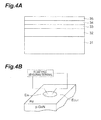
- An epitaxial substrate shown in Fig. 4A was produced by organometallic vapor phase epitaxy using an n-type semipolar GaN substrate 31.
- the primary surface of the GaN substrate 31 included an m-plane.
- An n-type GaN buffer layer 32 was formed on this primary surface.
- the epitaxial substrate Epi1 included a Si-doped n-type GaN layer 33, a Mg-doped GaN layer 34, and a high-concentration Mg-doped p-type GaN layer 35.
- the thickness of the Si-doped n-type GaN layer 33 was 1 ⁇ m.
- the thickness of the Mg-doped GaN layer 34 was 0.4 ⁇ m.
- the thickness of the high-concentration Mg-doped p-type GaN layer 35 was 50 nm.
- a resist was then formed by photolithography, prior to deposition of a metal film for a p-type electrode.
- This resist had an annular aperture.
- a Pd electrode was evaporated onto the epitaxial substrate by the electron beam method, in an evaporation system in vacuum of about 1 ⁇ 10 -6 Torr. The thickness of the Pd electrode was 500 ⁇ .
- the resist was lifted off using acetone. In this manner, a Pd electrode structure was produced as shown in Fig. 4B .
- This Pd electrode structure included an inside electrode E IN formed by photolithography, and an outside electrode E OUT isolated therefrom. The electrode structure with these electrodes was completed without being subjected to a thermal treatment.
- Fig. 5 is a graph showing the result of the measurement of contact resistance.
- Fig. 5 also shows the measurement result of contact resistance of a Ni/Au electrode structure produced by the same method as above. As shown in Fig. 5 , the contact resistance is effectively reduced by the Pd electrode structure of the present example, when compared to the NilAu electrode structure.
- An epitaxial substrate was produced according to the same procedure as in Example 1. This epitaxial substrate was subjected to ultrasonic organic cleaning using acetone and 2-propanol. Thereafter, it was cleaned with hydrochloric acid, aqua regia, and hydrofluoric acid, for five minutes each. A Pd electrode was evaporated onto this epitaxial substrate by the electron beam method. The thickness of the Pd electrode was 100 ⁇ . The temperature during the evaporation was room temperature. On the other hand, another epitaxial substrate was prepared by the production and cleaning methods of the same steps as the above epitaxial substrate. An NilAu electrode was evaporated onto this epitaxial substrate. Then this Ni/Au electrode was subjected to a thermal treatment. Ni was evaporated by the electron beam method.
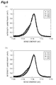
- Figs. 6 and 7 are graphs showing the results of the analysis of these epitaxial substrates.
- Part (a) and (b) of Fig. 6 show Ga 2p spectra.
- Part (a) and (b) of Fig. 7 show N 1s spectra.
- graphs G1 and G2 indicate spectra of the epitaxial substrate with the Pd electrode formed thereon.
- graphs G3 and G4 indicate spectra of the epitaxial substrate with the Ni/Au electrode formed thereon.
- a sub-peak exists on the higher energy side of the Ga 2p spectra of the epitaxial substrate with the Pd electrode thereon.
- Figs. 8 and 9 are transmission electron microscope photographs of cross sections of these epitaxial substrates.
- Part (a) of Fig. 8 shows the cross section of the epitaxial substrate on which the Pd electrode is formed and which was not subjected to a thermal treatment.
- Part (b) of Fig. 8 shows the cross section of the epitaxial substrate on which the Pd electrode is formed and which was subjected to the thermal treatment.
- the temperature of the thermal treatment is 310°C and the treating time is one minute.
- Part (a) and (b) of Fig. 9 show the cross sections of the epitaxial substrate with the Au/Ni electrode thereon.
- the thickness of the transition layer 19 is 0.5 nm. In contrast to it, the thickness of the transition layer 19 is increased to 2.0 nm in Part (b) of Fig. 8 . It is seen from this result that the transition layer spreads in the depth direction when the epitaxial substrate with the Pd electrode thereon is subjected to the thermal treatment. The contact resistance is slightly reduced between the Pd electrode and the GaN layer.
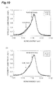
- Figs. 10 and 11 are graphs showing differences of spectra depending upon the presence/absence of a surface treatment, in the epitaxial substrate with the Pd electrode thereon.
- Part (a) and (b) of Fig. 10 show Ga 2p spectra.
- Part (a) and (b) of Fig. 11 show N 1s spectra.
- graphs G11 and G12 indicate spectra of the epitaxial substrate not subjected to the surface treatment.
- graphs G 13 to G16 indicate spectra of the epitaxial substrate subjected to the surface treatment.
- the height of a sub-peak of the epitaxial substrate subjected to the surface treatment is slightly higher than the height of a sub-peak of the epitaxial substrate not subjected to the surface treatment.
- the transition layer is suitably formed regardless of the presence/absence of the surface treatment, in the epitaxial substrate with the Pd electrode thereon.
- the Group III nitride semiconductor device of the present embodiment is a semiconductor optical device, e.g., such as a semiconductor laser or a light emitting diode.
- the Group III nitride semiconductor device of the present embodiment is a semiconductor device having the nonpolar or semipolar surface of the Group III nitride semiconductor doped with the p-type dopant, and the electrode formed on the nonpolar surface.
- the Group III nitride semiconductor device where the contact resistance between the semiconductor region and the electrode on the semiconductor region can be reduced, can be provided, when the Group III nitride semiconductor region has the surface inclined from the c-plane.
Landscapes
- Electrodes Of Semiconductors (AREA)
- Led Devices (AREA)
Abstract
Description
- The present invention relates to a Group III nitride semiconductor device.
- Patent Literatures 1 and 2 describe a method for forming an ohmic electrode on a p-type gallium nitride (GaN) layer grown on a (0001) plane or c-plane. In this method, Ni/Au film is evaporated onto the p-type GaN layer and thereafter a thermal treatment is carried out in an oxygen atmosphere. An oxide film exists on the surface of the p-type GaN layer, but nickel absorbs the oxide film by this method. Then nickel binds to oxygen atoms of the oxide film, thereby removing the oxide film. This allows gold to come into contact with the p-type GaN crystal, thereby forming an ohmic contact.
- Patent Literature 3 describes the result of an experiment. In this experiment, a p-type Group III nitride semiconductor layer is grown on a sapphire substrate. Then the substrate is heated to 300°C and thereafter platinum or nickel is evaporated onto a surface of the Group III nitride semiconductor layer. Thereafter, the contact resistance is measured.
- In the method described in Patent Literature 4, platinum is evaporated onto a p-type GaN contact layer. Then a thermal treatment is carried out in the range of 500°C to 600°C in an oxygen atmosphere to form an alloy electrode.
-
- Patent Literature 1: Japanese Unexamined Patent Application Publication No.
5-291621 - Patent Literature 2: Japanese Unexamined Patent Application Publication No.
9-64337 - Patent Literature 3: Japanese Unexamined Patent Application Publication No.
2004-247323 - Patent Literature 4: Japanese Unexamined Patent Application Publication No.
11-186605 - In production of Group III nitride-based semiconductor light emitting devices, depending upon the emission wavelength required, there are cases where a Group III nitride semiconductor containing indium, e.g., InGaN or InAlGaN, is grown on a Group III nitride semiconductor substrate, e.g., a GaN substrate. Since the diameter of indium atom is larger than the diameter of gallium atom, increase in the indium composition leads to increase in internal strain in the indium-containing layer because of lattice mismatch. As a result, a large piezoelectric field is induced in the layer, so as to decrease the recombination probability and thus reduce the luminous efficiency.
- A technology to solve this problem is to grow the indium-containing Group III nitride semiconductor on a plane largely inclined from the c-plane of the Group III nitride semiconductor crystal. The reason is that the piezoelectric field in the layer can be reduced by growing the indium-containing Group III nitride semiconductor on the plane largely inclined from the c-plane.
- In the case of the conventional ohmic electrodes described above, the contact resistance decreases when the electrode is formed on the primary surface of Group III nitride semiconductor parallel to the c-plane. However, the contact resistance increases when the electrode is formed on the primary surface of the Group III nitride semiconductor largely inclined from the c-plane. It is because a thick surface oxide film is formed when the primary surface of the Group III nitride semiconductor is largely inclined from the c-plane.
- The present invention provides the group III nitride semiconductor device that can reduce the contact resistance between the Group III nitride semiconductor and an electrode on the Group III nitride semiconductor when a surface of the Group III nitride semiconductor is inclined from the c-plane.
- In an aspect of the present invention, a group III nitride semiconductor device comprises (1) a semiconductor region having a surface comprised of a Group III nitride crystal, the semiconductor region being doped with a p-type dopant, the surface being one of a semipolar surface and a nonpolar surface, (2) a metal electrode provided on the surface, and (3) a transition layer formed between the Group III nitride crystal of the semiconductor region and the metal electrode, the transition layer being made by interdiffusion of a metal of the metal electrode and a Group III nitride of the semiconductor region.
- The inventors found that the contact resistance can be reduced effectively by the generation of the transition layer in an interface between the Group III nitride crystal and the electrode. When the surface of the Group III nitride semiconductor is nonpolar or semipolar, the Group III nitride crystal and the metal are likely to bind to each other on the surface. The transition layer is generated in between the semiconductor region and the electrode in the result, unlike the case of forming the electrode on the c-plane of the semiconductor region. The transition layer results from interdiffusion between the metal electrode and the Group III nitride crystal of the semiconductor region. The transition layer improves adhesion between the semiconductor region and the metal electrode, so as to decrease the contact resistance between them.
- A thickness of the transition layer may be more than or equal to 0.5 nm, and less than or equal to 3 nm. The contact resistance can be more effectively reduced by the transition layer in such thickness.
- The metal electrode may contain at least one of palladium and platinum. The transition layer is suitably made between the metal electrode and the semiconductor region by such metal electrode.
- The metal electrode may be completed without a thermal treatment process after forming a metal film on the surface. The transition layer is suitably made between the electrode and the semiconductor region by such electrode.
- An angle between a normal to the surface and a c-axis of the Group III nitride crystal constituting the semiconductor region may be in the range of 10 degrees to 80 degrees or the range of 100 degrees to 170 degrees. The semipolar surface of the semiconductor region can be provided hereby.
- An angle between a normal to the surface and a c-axis of the Group III nitride crystal constituting the semiconductor region may be in the range of 63 degrees to 80 degrees or the range of 100 degrees to 117 degrees. The semipolar surface of the semiconductor region can be provided hereby.
- The above object and other objects, features, and advantages of the present invention will more readily become apparent in view of the following detailed description of the preferred embodiments of the present invention proceeding with reference to the accompanying drawings.
- As explained above, according to an aspect of the present invention, the Group III nitride semiconductor device, where the contact resistance between the semiconductor region and the electrode on the semiconductor region can be reduced, can be provided, when the Group III nitride semiconductor region has the surface inclined from the c-plane.
-
-
Fig. 1 is a drawing showing major steps in a method for fabricating a Group III nitride semiconductor device according to an embodiment. -
Fig. 2 is a drawing schematically showing products in the major steps shown inFig. 1 . -
Fig. 3 is a drawing schematically showing products in the major steps shown inFig. 1 . -
Fig. 4A is a drawing showing a configuration of an epitaxial substrate produced in Example 1. -
Fig. 4B is a drawing showing a palladium electrode structure including an inside electrode formed by photolithography, and an outside electrode isolated from the inside electrode. -
Fig. 5 is a graph showing the results of measurements of contact resistances. -
Fig. 6 is a graph showing the results of analysis of epitaxial substrates in Example 2. -
Fig. 7 is a graph showing the results of analysis of epitaxial substrates in Example 2. -
Fig. 8 is a photograph of cross sections of the epitaxial substrates produced in Example 2. The photograph is taken with a transmission electron microscope. -
Fig. 9 is a photograph of cross sections of the epitaxial substrates produced in Example 2. The photograph is taken with a transmission electron microscope. -
Fig. 10 is a graph showing the difference of spectra depending upon the presence of a surface treatment process, in epitaxial substrates with palladium electrodes thereon. -
Fig. 11 is a graph showing the difference of spectra depending upon the presence of a surface treatment process, in epitaxial substrates with palladium electrodes thereon. - Embodiments of the Group III nitride semiconductor device according to the present invention will be described below in detail with reference to the accompanying drawings of
Figs. 1 to 11 . In the description of the drawings the same elements will be denoted by the same reference numerals, without redundant description. -
Fig. 1 is a drawing showing major steps in a method for fabricating a Group III nitride semiconductor device according to an embodiment.Figs. 2 and3 are drawings schematically showing products in the major steps shown inFig. 1 . The Group III nitride semiconductor device is an optical device, for example, such as a laser diode and a light emitting diode, or an electronic device, for example, such as a pn junction diode and a transistor. - Step S101 in
Fig. 1 is to prepare asubstrate 11 shown in Part (a) ofFig. 2 . In a preferred embodiment, thesubstrate 11 has a nonpolar or semipolar primary surface. Thesubstrate 11 is comprised, for example, of Group III nitride semiconductor of the wurtzite structure. Examples of such Group III nitride semiconductors include AlN, gallium nitride-based semiconductors such as AlGaN and GaN, and so on. With use of these GaN-based semiconductors, theprimary surface 11a of thesubstrate 11 has nonpolar or semipolar nature. The axis Cx shown in Part (a) ofFig. 2 indicates a direction of the c-axis (<0001> axis) of the Group III nitride semiconductor of thesubstrate 11, and the direction of the axis Cx is represented by a c-axis vector VC. A normal vector NV is normal to theprimary surface 11a of thesubstrate 11. An angle Alpha between the normal vector NV on thesubstrate 11 and the c-axis vector VC is, for example, in the range of not less than 10 degrees and not more than 170 degrees. - In step S102, the
substrate 11 is placed in aprocessing device 10a such as a growth furnace, as shown in Part (b) ofFig. 2 . Thereafter, asemiconductor region 13 is grown on theprimary surface 11a of thesubstrate 11. Thesemiconductor region 13 is comprised of Group III nitride crystal. Thesemiconductor region 13 preferably includes, for example, a GaN-based semiconductor layer or a plurality of GaN-based semiconductor layers. In the present embodiment, thesemiconductor region 13 is provided by epitaxial growth on theprimary surface 11a of thesubstrate 11. This crystal growth is carried out, for example, by organometallic vapor phase epitaxy or by molecular beam epitaxy. Atop surface 13a of thesemiconductor region 13 has nonpolar or semipolar nature. Thesurface 13a of thesemiconductor region 13 is comprised of p-type Group III nitride semiconductor, e.g., GaN-based semiconductor. The p-type Group III nitride semiconductor is doped with a high concentration of a p-type dopant, e.g., Mg. It should be noted that the formation of the p-type Group III nitride semiconductor is not limited only to the epitaxial growth. These steps result in producing a first substrate product P1. - Step S103 is to take the first substrate product P1 out of the
processing device 10a. At this time, thesurface 13a of thesemiconductor region 13 exposed to the atmosphere is more likely to be oxidized than a polar surface as the c-plane. Namely, a relatively thick native oxide film is formed on the nonpolar or semipolar surface of thesemiconductor region 13 exposed to the atmosphere. The native oxide film is formed during transportation of the substrate product P1 from theprocessing device 10a to a film-forming device. As shown in Part (c) ofFig. 2 , an oxidizedproduct 15 of the native oxide film exists on the surface of the first substrate product P1. - If needed, a step to perform a pretreatment of the first substrate product P1 may be optionally provided as step S104. It is preferable to use, for example, at least one of aqua regia, hydrofluoric acid, and hydrochloric acid as a solution for the pretreatment. The pretreatment using these solutions can remove the oxidized
product 15 formed on thesurface 13a of thesemiconductor region 13, to some extent. - Thereafter, step S105 is carried out to place the first substrate product P1 in the film-forming
device 10b, as shown in Part (a) ofFig. 3 . - If needed, a mask for a lift-off procedure can be formed on the first substrate product P1, prior to the placement thereof in the film-forming
device 10b. This mask includes a resist layer. Immediately after the substrate product P1 is placed in the film-formingdevice 10b, the film-formingdevice 10b is vacuumized down to the vacuum degree of about 1 × 10⁻⁶ Torr. It is noted that 1 Pa is equivalent to 0.0075 Torr. As shown in Part (b) ofFig. 3 , stepS 106 is to deposit a film ofmetal electrode 17 on the surface of the first substrate product P1, using the film-formingdevice 10b. Themetal electrode 17 can be formed, for example, by electron beam evaporation or by resistive heating. The temperature of thesubstrate 11 at this time is preferably, for example, not less than 15 degrees and not more than 100 degrees. Themetal electrode 17 contains Pd. In an example, themetal electrode 17 is comprised of a Pd layer. The thickness of the Pd layer is preferably, for example, more than or equal to 10 nm. - When the
metal electrode 17 is deposited, atransition layer 19 is made at an interface between themetal electrode 17 and thesurface 13a of thesemiconductor region 13. Thetransition layer 19 is a layer resulting from interdiffusion of Pd and GaN. Thetransition layer 19 is made at the same time as the deposition of themetal electrode 17. In the present embodiment, since thesurface 13a of thesemiconductor region 13 is nonpolar or semipolar, it is likely to bind to metal, different from the c-plane, and thussuch transition layer 19 spreads. - The formation of the
metal electrode 17 results in forming an ohmic electrode in electric contact with thesurface 13a of thesemiconductor region 13. This step results in producing a second substrate product P2. The substrate product P2 includes themetal electrode 17 provided on thesemiconductor region 13 of the substrate product P1, and thetransition layer 19 made at the interface between thesemiconductor region 13 and themetal electrode 17. - Step S107 is to take the second substrate product P2 out of the film-forming
device 10b. If the mask for the lift-off procedure is formed on the first substrate product P1, a step to perform the lift-off procedure is carried out to form a patterned electrode. The lift-off procedure is carried out, for example, using acetone or the like. - After that, it is common practice to perform a thermal treatment at about 400°C with the second substrate product P2 being placed in a thermal treatment device. However, the present embodiment does not involve such a thermal treatment to complete the formation of the ohmic electrode. Then the second substrate product P2 is cut in a chip form. This completes the Group III nitride semiconductor device.
- The below will describe the advantageous effects achieved by the Group III nitride semiconductor device and its fabrication method of the present embodiment described above.
- The inventors attempted to form an electrode on a nonpolar or semipolar plane of GaN, using the conventional technology (Patent Literatures 1 and 2) for forming the ohmic electrode on the c-plane of GaN crystal. However, for example, when Ni/Au metal film was formed on a nonpolar or semipolar plane of GaN, e.g., a (11-22) plane and the metal film was alloyed in an oxygen atmosphere, the contact resistance of the ohmic electrode was not reduced. When a Pt electrode was made on a nonpolar or semipolar plane at high temperature as in the other conventional technology (Patent Literatures 3 and 4), no ohmic contact was achieved. Namely, it became clear that these conventional technologies allowed a good ohmic electrode to be formed on the c-plane of GaN crystal, but hardly allowed a good ohmic electrode to be formed on a nonpolar plane or a semipolar plane.
- Then, the inventors produced a Pd electrode on a nonpolar plane and a semipolar plane of GaN crystal at low temperature. As a result, a good ohmic contact was achieved. For finding the reason for it, a surface analysis was conducted with an X-ray photoelectron spectrometer (XPS). It was confirmed by this analysis that the Pd electrode formed at low temperature on the nonpolar or semipolar plane of GaN crystal provided a sub-peak which was not observed with the other electrodes. It is considered that a transition layer resulting from interdiffusion of Pd and GaN was newly made between the nonpolar or semipolar plane of GaN crystal and the Pd electrode and it improved the contact resistance between the GaN crystal and the Pd electrode. A bonding state of a crystal surface on the nonpolar or semipolar plane is different from that on the c-plane. GaN and Pd are likely to bind to each other on the nonpolar or semipolar plane. It is thus presumed that the transition layer as described above spread at the interface between the GaN crystal and the Pd electrode. This phenomenon is considered to occur in the same manner in the Group III nitride semiconductors other than GaN.
- In this embodiment, as described above, the
semiconductor region 13 has thesurface 13a, which is nonpolar or semipolar. As themetal electrode 17 containing Pd is formed on thesurface 13a, thetransition layer 19 is made. Thetransition layer 19 improves adhesion between thesemiconductor region 13 and themetal electrode 17, so as to decrease the contact resistance between them. - The thickness of the
transition layer 19 is preferably more than or equal to 0.5 nm and less than or equal to 3 nm. The inventors investigated a relation between the thickness of thetransition layer 19 and electrical characteristics. As a result, good electrical characteristics were obtained in the thickness range of more than or equal to 0.5 nm and less than or equal to 3 nm. Namely, the contact resistance can be more effectively reduced by thetransition layer 19 in such thickness. - The
metal electrode 17 preferably contains Pd. The reason for it is that thetransition layer 19 is suitably made between themetal electrode 17 and thesemiconductor region 13 when themetal electrode 17 contains Pd. It is, however, noted that the metal to form thetransition layer 19 is not limited only to Pd. For example, the transition layer can be made by the metal electrode containing Pt. - The
metal electrode 17 is preferably completed without being subjected to a thermal treatment, after the metal film is formed on thesurface 13a of thesemiconductor region 13. This permits thetransition layer 19 to be suitably made between themetal electrode 17 and thesemiconductor region 13. - An epitaxial substrate shown in
Fig. 4A was produced by organometallic vapor phase epitaxy using an n-typesemipolar GaN substrate 31. The primary surface of theGaN substrate 31 included an m-plane. An n-typeGaN buffer layer 32 was formed on this primary surface. The epitaxial substrate Epi1 included a Si-doped n-type GaN layer 33, a Mg-dopedGaN layer 34, and a high-concentration Mg-doped p-type GaN layer 35. The thickness of the Si-doped n-type GaN layer 33 was 1 µm. The thickness of the Mg-dopedGaN layer 34 was 0.4 µm. The thickness of the high-concentration Mg-doped p-type GaN layer 35 was 50 nm. These GaN-based semiconductor layers were grown in order on thesubstrate 31. - A resist was then formed by photolithography, prior to deposition of a metal film for a p-type electrode. This resist had an annular aperture. Thereafter, a Pd electrode was evaporated onto the epitaxial substrate by the electron beam method, in an evaporation system in vacuum of about 1×10⁻⁶ Torr. The thickness of the Pd electrode was 500 Å. The resist was lifted off using acetone. In this manner, a Pd electrode structure was produced as shown in
Fig. 4B . This Pd electrode structure included an inside electrode EIN formed by photolithography, and an outside electrode EOUT isolated therefrom. The electrode structure with these electrodes was completed without being subjected to a thermal treatment. - The contact resistance of the electrode was measured using this electrode structure.
Fig. 5 is a graph showing the result of the measurement of contact resistance.Fig. 5 also shows the measurement result of contact resistance of a Ni/Au electrode structure produced by the same method as above. As shown inFig. 5 , the contact resistance is effectively reduced by the Pd electrode structure of the present example, when compared to the NilAu electrode structure. - An epitaxial substrate was produced according to the same procedure as in Example 1. This epitaxial substrate was subjected to ultrasonic organic cleaning using acetone and 2-propanol. Thereafter, it was cleaned with hydrochloric acid, aqua regia, and hydrofluoric acid, for five minutes each. A Pd electrode was evaporated onto this epitaxial substrate by the electron beam method. The thickness of the Pd electrode was 100 Å. The temperature during the evaporation was room temperature. On the other hand, another epitaxial substrate was prepared by the production and cleaning methods of the same steps as the above epitaxial substrate. An NilAu electrode was evaporated onto this epitaxial substrate. Then this Ni/Au electrode was subjected to a thermal treatment. Ni was evaporated by the electron beam method. Au was evaporated by resistive heating. The thickness of each of Ni and Au layers was 50Å. In this manner, the different types of p-type electrodes were made on the two respective epitaxial substrates. An analysis was conducted to analyze the interface between the GaN crystal and the p-type electrode in these epitaxial substrates. This analysis was carried out with the X-ray photoelectron spectrometer.
-
Figs. 6 and7 are graphs showing the results of the analysis of these epitaxial substrates. Part (a) and (b) ofFig. 6 show Ga 2p spectra. Part (a) and (b) ofFig. 7 show N 1s spectra. InFigs. 6 and7 , graphs G1 and G2 indicate spectra of the epitaxial substrate with the Pd electrode formed thereon. InFigs. 6 and7 , graphs G3 and G4 indicate spectra of the epitaxial substrate with the Ni/Au electrode formed thereon. As shown in Part (a) and (b) ofFig. 6 , a sub-peak exists on the higher energy side of the Ga 2p spectra of the epitaxial substrate with the Pd electrode thereon. However, no such peak exists in the Ga 2p spectra of the epitaxial substrate with the Ni/Au electrode thereon. This confirms that a new layer except for the GaN crystal, i.e., the transition layer is made in the epitaxial substrate with the Pd electrode thereon. -
Figs. 8 and9 are transmission electron microscope photographs of cross sections of these epitaxial substrates. Part (a) ofFig. 8 shows the cross section of the epitaxial substrate on which the Pd electrode is formed and which was not subjected to a thermal treatment. Part (b) ofFig. 8 shows the cross section of the epitaxial substrate on which the Pd electrode is formed and which was subjected to the thermal treatment. The temperature of the thermal treatment is 310°C and the treating time is one minute. Part (a) and (b) ofFig. 9 show the cross sections of the epitaxial substrate with the Au/Ni electrode thereon. - As shown in Part (a) and (b) of
Fig. 8 , it is confirmed that a thin new layer, or thetransition layer 19 is formed between the Pd electrode and the GaN layer in the epitaxial substrate with the Pd electrode thereon. However, as shown in Part (a) and (b) ofFig. 9 , no such layer is recognized in the epitaxial substrate with the Ni/Au electrode thereon. In Part (a) ofFig. 8 , the thickness of thetransition layer 19 is 0.5 nm. In contrast to it, the thickness of thetransition layer 19 is increased to 2.0 nm in Part (b) ofFig. 8 . It is seen from this result that the transition layer spreads in the depth direction when the epitaxial substrate with the Pd electrode thereon is subjected to the thermal treatment. The contact resistance is slightly reduced between the Pd electrode and the GaN layer. -
Figs. 10 and11 are graphs showing differences of spectra depending upon the presence/absence of a surface treatment, in the epitaxial substrate with the Pd electrode thereon. Part (a) and (b) ofFig. 10 show Ga 2p spectra. Part (a) and (b) ofFig. 11 show N 1s spectra. InFigs. 10 and11 , graphs G11 and G12 indicate spectra of the epitaxial substrate not subjected to the surface treatment. InFigs. 10 and11 ,graphs G 13 to G16 indicate spectra of the epitaxial substrate subjected to the surface treatment. - As shown in
Figs. 10 and11 , the height of a sub-peak of the epitaxial substrate subjected to the surface treatment is slightly higher than the height of a sub-peak of the epitaxial substrate not subjected to the surface treatment. However, there is little difference in band bending between these epitaxial substrates. Namely, the transition layer is suitably formed regardless of the presence/absence of the surface treatment, in the epitaxial substrate with the Pd electrode thereon. - The Group III nitride semiconductor device of the present embodiment is a semiconductor optical device, e.g., such as a semiconductor laser or a light emitting diode. The Group III nitride semiconductor device of the present embodiment is a semiconductor device having the nonpolar or semipolar surface of the Group III nitride semiconductor doped with the p-type dopant, and the electrode formed on the nonpolar surface.
- The principle of the present invention was illustrated and explained in the preferred embodiments, but it is recognized by those skilled in the art that the present invention can be modified in arrangement and detail without departing from the principle. The present invention is by no means limited to the specific configurations disclosed in the embodiments. Therefore, the applicant claims all modifications and changes falling within the scope of claims and resulting from the scope of spirit thereof.
- As explained above, according to the embodiments, the Group III nitride semiconductor device, where the contact resistance between the semiconductor region and the electrode on the semiconductor region can be reduced, can be provided, when the Group III nitride semiconductor region has the surface inclined from the c-plane.
-
- 11
- substrate
- 11a
- primary surface
- Cx
- axis
- VC
- c-axis vector
- NV
- normal vector
- Alpha
- angle
- 10a
- processing device
- 10b
- film-forming device
- 13
- semiconductor region
- 13a
- surface
- P1, P2
- substrate product
- 15
- oxidized product
- 17
- metal electrode
- 19
- transition layer
Claims (6)
- A Group III nitride semiconductor device comprising:a semiconductor region having a surface comprised of a Group III nitride crystal, the semiconductor region being doped with a p-type dopant, the surface being one of a semipolar surface and a nonpolar surface;a metal electrode provided on the surface; anda transition layer formed between the Group III nitride crystal of the semiconductor region and the metal electrode, the transition layer being made by interdiffusion of a metal of the metal electrode and a Group III nitride of the semiconductor region.
- The Group III nitride semiconductor device according to claim 1,
wherein a thickness of the transition layer is more than or equal to 0.5 nm, and less than or equal to 3 nm. - The Group III nitride semiconductor device according to claim 1 or 2,
wherein the metal electrode contains at least one of palladium and platinum. - The Group III nitride semiconductor device according to any one of claims 1 to 3,
wherein the metal electrode is completed without a thermal treatment process after forming a metal film on the surface. - The Group III nitride semiconductor device according to any one of claims 1 to 4,
wherein an angle between a normal to the surface and a c-axis of the Group III nitride crystal constituting the semiconductor region is in the range of 10 degrees to 80 degrees or the range of 100 degrees to 170 degrees. - The Group III nitride semiconductor device according to any one of claims 1 to 4,
wherein an angle between a normal to the surface and a c-axis of the Group III nitride crystal constituting the semiconductor region is in the range of 63 degrees to 80 degrees or the range of 100 degrees to 117 degrees.
Applications Claiming Priority (2)
| Application Number | Priority Date | Filing Date | Title |
|---|---|---|---|
| JP2010008232A JP2011146639A (en) | 2010-01-18 | 2010-01-18 | Group iii nitride-based semiconductor element |
| PCT/JP2010/066443 WO2011086730A1 (en) | 2010-01-18 | 2010-09-22 | Group iii nitride semiconductor element |
Publications (2)
| Publication Number | Publication Date |
|---|---|
| EP2528117A1 true EP2528117A1 (en) | 2012-11-28 |
| EP2528117A4 EP2528117A4 (en) | 2013-08-07 |
Family
ID=44276973
Family Applications (1)
| Application Number | Title | Priority Date | Filing Date |
|---|---|---|---|
| EP10843086.9A Withdrawn EP2528117A4 (en) | 2010-01-18 | 2010-09-22 | SEMI-CONDUCTOR ELEMENT GROUP III ELEMENT NITRIDE |
Country Status (7)
| Country | Link |
|---|---|
| US (1) | US8415707B2 (en) |
| EP (1) | EP2528117A4 (en) |
| JP (1) | JP2011146639A (en) |
| KR (1) | KR20110099682A (en) |
| CN (1) | CN102422446A (en) |
| TW (1) | TW201131805A (en) |
| WO (1) | WO2011086730A1 (en) |
Families Citing this family (3)
| Publication number | Priority date | Publication date | Assignee | Title |
|---|---|---|---|---|
| JP5403024B2 (en) * | 2011-09-12 | 2014-01-29 | 住友電気工業株式会社 | Method for fabricating nitride semiconductor light emitting device |
| EP2811526B1 (en) | 2012-01-30 | 2020-11-18 | National Institute for Materials Science | AlN MONOCRYSTALLINE SCHOTTKY BARRIER DIODE AND METHOD FOR PRODUCING SAME |
| KR101843513B1 (en) * | 2012-02-24 | 2018-03-29 | 서울바이오시스 주식회사 | Gallium nitride-based light emitting diode |
Family Cites Families (21)
| Publication number | Priority date | Publication date | Assignee | Title |
|---|---|---|---|---|
| JP2778349B2 (en) | 1992-04-10 | 1998-07-23 | 日亜化学工業株式会社 | Gallium nitride based compound semiconductor electrodes |
| JP3620926B2 (en) | 1995-06-16 | 2005-02-16 | 豊田合成株式会社 | P-conducting group III nitride semiconductor electrode, electrode forming method and device |
| WO1997026680A1 (en) * | 1996-01-19 | 1997-07-24 | Matsushita Electric Industrial Co., Ltd. | Gallium nitride compound semiconductor light emitting device and process for producing gallium nitride compound semiconductor |
| JP3555419B2 (en) | 1997-12-18 | 2004-08-18 | 豊田合成株式会社 | Gallium nitride based compound semiconductor electrode forming method and device manufacturing method |
| JP4063050B2 (en) | 2002-10-31 | 2008-03-19 | 豊田合成株式会社 | Electrode of p-type group III nitride compound semiconductor and method for producing the same |
| JP4396816B2 (en) * | 2003-10-17 | 2010-01-13 | 日立電線株式会社 | Group III nitride semiconductor substrate and manufacturing method thereof |
| KR100586943B1 (en) * | 2003-12-26 | 2006-06-07 | 삼성전기주식회사 | Method of manufacturing gallium nitride-based semiconductor light emitting device |
| JP4999278B2 (en) * | 2004-02-24 | 2012-08-15 | 昭和電工株式会社 | Gallium nitride compound semiconductor light emitting device |
| US20070170461A1 (en) * | 2004-02-24 | 2007-07-26 | Koji Kamei | Gallium nitride-based compound semiconductor light-emitting device |
| JP2006013474A (en) * | 2004-05-26 | 2006-01-12 | Showa Denko Kk | Gallium nitride based compound semiconductor light emitting device |
| US8049243B2 (en) * | 2004-05-26 | 2011-11-01 | Showa Denko K.K. | Gallium nitride-based compound semiconductor light emitting device |
| US7858996B2 (en) * | 2006-02-17 | 2010-12-28 | The Regents Of The University Of California | Method for growth of semipolar (Al,In,Ga,B)N optoelectronic devices |
| KR101351396B1 (en) * | 2005-06-01 | 2014-02-07 | 재팬 사이언스 앤드 테크놀로지 에이젼시 | Technique for the growth and fabrication of semipolar (Ga,Al,In,B)N thin films, heterostructures, and devices |
| JP4978009B2 (en) * | 2006-01-16 | 2012-07-18 | ソニー株式会社 | GaN-based semiconductor light-emitting device and manufacturing method thereof |
| KR101452550B1 (en) * | 2007-07-19 | 2014-10-21 | 미쓰비시 가가꾸 가부시키가이샤 | Ⅲ nitride semiconductor substrate and method for cleaning the same |
| US7973321B2 (en) * | 2007-11-05 | 2011-07-05 | Rohm Co., Ltd. | Nitride semiconductor light emitting device having ridge parts |
| JP2009158745A (en) * | 2007-12-27 | 2009-07-16 | Mitsubishi Electric Corp | Manufacturing method of semiconductor device |
| JP5003527B2 (en) | 2008-02-22 | 2012-08-15 | 住友電気工業株式会社 | Group III nitride light emitting device and method for fabricating group III nitride semiconductor light emitting device |
| JP2009231609A (en) | 2008-03-24 | 2009-10-08 | Sumitomo Electric Ind Ltd | Production method of semiconductor light-emitting element |
| JP4390007B2 (en) * | 2008-04-07 | 2009-12-24 | 住友電気工業株式会社 | Group III nitride semiconductor device and epitaxial wafer |
| JP4917585B2 (en) * | 2008-08-26 | 2012-04-18 | 住友電気工業株式会社 | Method for manufacturing nitride-based semiconductor optical device and method for manufacturing epitaxial wafer |
-
2010
- 2010-01-18 JP JP2010008232A patent/JP2011146639A/en active Pending
- 2010-07-13 US US12/834,977 patent/US8415707B2/en not_active Expired - Fee Related
- 2010-09-22 KR KR1020117010827A patent/KR20110099682A/en not_active Ceased
- 2010-09-22 EP EP10843086.9A patent/EP2528117A4/en not_active Withdrawn
- 2010-09-22 CN CN2010800209125A patent/CN102422446A/en active Pending
- 2010-09-22 WO PCT/JP2010/066443 patent/WO2011086730A1/en not_active Ceased
- 2010-10-13 TW TW099134951A patent/TW201131805A/en unknown
Also Published As
| Publication number | Publication date |
|---|---|
| KR20110099682A (en) | 2011-09-08 |
| WO2011086730A1 (en) | 2011-07-21 |
| JP2011146639A (en) | 2011-07-28 |
| US8415707B2 (en) | 2013-04-09 |
| EP2528117A4 (en) | 2013-08-07 |
| TW201131805A (en) | 2011-09-16 |
| CN102422446A (en) | 2012-04-18 |
| US20110175201A1 (en) | 2011-07-21 |
Similar Documents
| Publication | Publication Date | Title |
|---|---|---|
| JP2002016311A (en) | Gallium nitride based light emitting device | |
| CN101188262B (en) | Nitride semiconductor light emitting device | |
| JP4023121B2 (en) | N-type electrode, group III nitride compound semiconductor device, method for manufacturing n-type electrode, and method for manufacturing group III nitride compound semiconductor device | |
| US20120298954A1 (en) | Semiconductor light emitting device and manufacturing method of the same | |
| US20140138614A1 (en) | Semiconductor light emitting device | |
| WO2007091651A1 (en) | Nitride semiconductor element | |
| JP3603713B2 (en) | Method of growing group III nitride compound semiconductor film and group III nitride compound semiconductor device | |
| JP2015153826A (en) | Nitride semiconductor light emitting element and manufacturing method of the same | |
| CN112750925B (en) | Deep ultraviolet LED device structure and preparation method thereof | |
| JP5103979B2 (en) | Electrode forming method for group III nitride compound semiconductor and method for producing p-type group III nitride compound semiconductor | |
| JP5471485B2 (en) | Nitride semiconductor device and pad electrode manufacturing method for nitride semiconductor device | |
| JPH1012567A (en) | Group III nitride semiconductor electrode and device having the electrode | |
| US8415707B2 (en) | Group III nitride semiconductor device | |
| JP5130436B2 (en) | GaN-based semiconductor light-emitting device and manufacturing method thereof | |
| JP5749888B2 (en) | Semiconductor device and method for manufacturing the semiconductor device | |
| JP2001015852A (en) | Electrode structure on p-type group III nitride semiconductor layer and method of forming the same | |
| JP2010245109A (en) | Group III nitride semiconductor device and method for producing electrode | |
| JP5136615B2 (en) | Method for manufacturing group III nitride semiconductor light emitting device | |
| US20070096126A1 (en) | Gallium nitride-based compound semiconductor light-emitting device and negative electrode thereof | |
| JP5482771B2 (en) | Method for manufacturing group III nitride semiconductor light emitting device | |
| CN109346587B (en) | GaN light-emitting diode, preparation method thereof and LED chip | |
| TWI387134B (en) | Light-emitting device and method for manufacturing the same | |
| WO2007119919A1 (en) | Iii-nitride semiconductor light emitting device and method for manufacturing the same | |
| CN102945903A (en) | Semiconductor device and method of fabricating the same | |
| KR20050081208A (en) | Growth of single nitride-based semiconductors using substrate decomposition prevention layer and manufacturing of high-quality nitride-based light emitting devices |
Legal Events
| Date | Code | Title | Description |
|---|---|---|---|
| PUAI | Public reference made under article 153(3) epc to a published international application that has entered the european phase |
Free format text: ORIGINAL CODE: 0009012 |
|
| 17P | Request for examination filed |
Effective date: 20110818 |
|
| AK | Designated contracting states |
Kind code of ref document: A1 Designated state(s): AL AT BE BG CH CY CZ DE DK EE ES FI FR GB GR HR HU IE IS IT LI LT LU LV MC MK MT NL NO PL PT RO SE SI SK SM TR |
|
| DAX | Request for extension of the european patent (deleted) | ||
| A4 | Supplementary search report drawn up and despatched |
Effective date: 20130705 |
|
| RIC1 | Information provided on ipc code assigned before grant |
Ipc: H01L 33/14 20100101ALI20130701BHEP Ipc: H01L 33/40 20100101ALI20130701BHEP Ipc: H01L 33/32 20100101AFI20130701BHEP Ipc: H01L 29/45 20060101ALI20130701BHEP Ipc: H01L 21/28 20060101ALI20130701BHEP |
|
| STAA | Information on the status of an ep patent application or granted ep patent |
Free format text: STATUS: THE APPLICATION IS DEEMED TO BE WITHDRAWN |
|
| 18D | Application deemed to be withdrawn |
Effective date: 20140204 |