EP2525486B1 - Method for operating a drive control device and drive control device operating by the method - Google Patents
Method for operating a drive control device and drive control device operating by the method Download PDFInfo
- Publication number
- EP2525486B1 EP2525486B1 EP11166214.4A EP11166214A EP2525486B1 EP 2525486 B1 EP2525486 B1 EP 2525486B1 EP 11166214 A EP11166214 A EP 11166214A EP 2525486 B1 EP2525486 B1 EP 2525486B1
- Authority
- EP
- European Patent Office
- Prior art keywords
- control signal
- signal time
- control
- control device
- time instants
- Prior art date
- Legal status (The legal status is an assumption and is not a legal conclusion. Google has not performed a legal analysis and makes no representation as to the accuracy of the status listed.)
- Active
Links
- 238000000034 method Methods 0.000 title claims description 29
- 239000004065 semiconductor Substances 0.000 claims description 40
- 230000005540 biological transmission Effects 0.000 claims description 29
- 238000004590 computer program Methods 0.000 claims description 8
- 230000006870 function Effects 0.000 claims 2
- 239000000872 buffer Substances 0.000 claims 1
- 238000004364 calculation method Methods 0.000 claims 1
- 238000000926 separation method Methods 0.000 description 6
- 230000001419 dependent effect Effects 0.000 description 2
- 230000000694 effects Effects 0.000 description 2
- 230000001105 regulatory effect Effects 0.000 description 2
- 230000002123 temporal effect Effects 0.000 description 2
- 230000003139 buffering effect Effects 0.000 description 1
- 238000006073 displacement reaction Methods 0.000 description 1
- 230000002349 favourable effect Effects 0.000 description 1
- 231100001261 hazardous Toxicity 0.000 description 1
- 230000008054 signal transmission Effects 0.000 description 1
Images


Classifications
-
- G—PHYSICS
- G05—CONTROLLING; REGULATING
- G05B—CONTROL OR REGULATING SYSTEMS IN GENERAL; FUNCTIONAL ELEMENTS OF SUCH SYSTEMS; MONITORING OR TESTING ARRANGEMENTS FOR SUCH SYSTEMS OR ELEMENTS
- G05B11/00—Automatic controllers
- G05B11/01—Automatic controllers electric
-
- H—ELECTRICITY
- H02—GENERATION; CONVERSION OR DISTRIBUTION OF ELECTRIC POWER
- H02M—APPARATUS FOR CONVERSION BETWEEN AC AND AC, BETWEEN AC AND DC, OR BETWEEN DC AND DC, AND FOR USE WITH MAINS OR SIMILAR POWER SUPPLY SYSTEMS; CONVERSION OF DC OR AC INPUT POWER INTO SURGE OUTPUT POWER; CONTROL OR REGULATION THEREOF
- H02M1/00—Details of apparatus for conversion
- H02M1/44—Circuits or arrangements for compensating for electromagnetic interference in converters or inverters
-
- H—ELECTRICITY
- H02—GENERATION; CONVERSION OR DISTRIBUTION OF ELECTRIC POWER
- H02M—APPARATUS FOR CONVERSION BETWEEN AC AND AC, BETWEEN AC AND DC, OR BETWEEN DC AND DC, AND FOR USE WITH MAINS OR SIMILAR POWER SUPPLY SYSTEMS; CONVERSION OF DC OR AC INPUT POWER INTO SURGE OUTPUT POWER; CONTROL OR REGULATION THEREOF
- H02M7/00—Conversion of ac power input into dc power output; Conversion of dc power input into ac power output
- H02M7/42—Conversion of dc power input into ac power output without possibility of reversal
- H02M7/44—Conversion of dc power input into ac power output without possibility of reversal by static converters
- H02M7/48—Conversion of dc power input into ac power output without possibility of reversal by static converters using discharge tubes with control electrode or semiconductor devices with control electrode
- H02M7/53—Conversion of dc power input into ac power output without possibility of reversal by static converters using discharge tubes with control electrode or semiconductor devices with control electrode using devices of a triode or transistor type requiring continuous application of a control signal
- H02M7/537—Conversion of dc power input into ac power output without possibility of reversal by static converters using discharge tubes with control electrode or semiconductor devices with control electrode using devices of a triode or transistor type requiring continuous application of a control signal using semiconductor devices only, e.g. single switched pulse inverters
- H02M7/5387—Conversion of dc power input into ac power output without possibility of reversal by static converters using discharge tubes with control electrode or semiconductor devices with control electrode using devices of a triode or transistor type requiring continuous application of a control signal using semiconductor devices only, e.g. single switched pulse inverters in a bridge configuration
- H02M7/53871—Conversion of dc power input into ac power output without possibility of reversal by static converters using discharge tubes with control electrode or semiconductor devices with control electrode using devices of a triode or transistor type requiring continuous application of a control signal using semiconductor devices only, e.g. single switched pulse inverters in a bridge configuration with automatic control of output voltage or current
- H02M7/53873—Conversion of dc power input into ac power output without possibility of reversal by static converters using discharge tubes with control electrode or semiconductor devices with control electrode using devices of a triode or transistor type requiring continuous application of a control signal using semiconductor devices only, e.g. single switched pulse inverters in a bridge configuration with automatic control of output voltage or current with digital control
Definitions
- the invention relates to a method for operating a drive control device and to a drive control device operating according to the method, and to a computer program for implementing the method, and thus also to a drive control device having means for executing such a computer program.
- the invention relates to a method for operating a drive control device, wherein it has an inverter and wherein this comprises controllable by control signals semiconductor switch.
- Such drive control devices are known per se.
- the inverters generate an output voltage of variable frequency and voltage due to the drive by the drive signals.
- the rotational speed and the torque, for example, of an electric motor can be set and regulated as a load of the drive control device.
- a control electronics for generating the drive signals is on a low voltage side of the drive control device and the inverter in contrast on a high voltage side.
- There is potential separation between the low voltage and high voltage side for safety reasons.
- the control signals must be transmitted across this potential separation.
- a serial transmission has been considered.
- the disadvantage here is that due to high voltage gradients when switching the semiconductor switch shift currents between the high and low voltage side can result.
- a method for operating a drive control device and a drive control device operating according to the method are known in which a parameterisable ASIC for generating the drive signals is provided on the high-voltage side.
- the parameterization takes place on the basis of data which is transmitted to the ASIC located on the high-voltage side from the low-voltage side by means of a serial data transmission.
- Inverters with semiconductor switches which can be controlled by drive signals, provide that a drive logic determines a drive signal time for each drive signal and the drive signal times in operation from a low voltage side of the drive control device with the drive logic to a high voltage side of the drive control device be transmitted to the inverter, and that the transmission of Anêtsignalzeit exist between switching points of the switching elements of the semiconductor switch remaining switching pauses takes place and that based on the transmitted Anêtsignalzeitfound on the high voltage side driving signals for driving the semiconductor switches are generated.
- the advantage of the invention is that disturbances due to switching operations of the semiconductor switches are avoided by the transmission of the Anberichtsignalzeitfound during the switching pauses of the semiconductor switches. Disruptions due namely, the above-mentioned shift currents occur only when the semiconductor switches switch. If the time of transmission is chosen such that no semiconductor switches switch, the displacement currents can no longer disturb the transmission of the control signal instants.
- a determination of a position and length of switching pauses of the semiconductor switches can be done by the control logic together with the determination of the An Kunststoffsignalzeitfound, because with the determined An Kunststoffsignalzeitticianen is a position of the switching points of the semiconductor switch and a period between each remaining period and thus immediately information regarding the position and length of Switching breaks before.
- the transmission of the An Kunststoffsignalzeitfound during the switching pauses of the semiconductor switches can thus be performed or initiated in a particularly favorable manner by the control logic.
- the drive signal times are transmitted by the drive logic to a drive circuit on the high voltage side of the drive control device, that the drive circuit temporarily stores the transmitted drive signal times that the drive circuit stores the latched drive signal times with the value of a timer, a clock, counter or the like - hereinafter collectively referred to as a timer - compares and that in each case a drive signal is generated depending on the result of the comparison by the drive circuit.
- a timer - compares and that in each case a drive signal is generated depending on the result of the comparison by the drive circuit.
- a serial transmission also allows the combination of several control signal times to form a telegram.
- known methods for detecting transmission errors can be used so that a retransmission can be initiated if a fault of a transmission is detected.
- a switching interval is the period between two switching points of a semiconductor switch. The switching interval thus includes the switching pause.
- the above-mentioned object is also achieved with a drive control device which operates according to the method as described here and below and for this purpose comprises means for carrying out the method.
- the method and possibly embodiments are or are preferably implemented in software.
- the invention is thus on the one hand also a computer program with program code instructions executable by a computer and on the other hand a storage medium with such a computer program and finally also a drive control device in whose memory such a computer program is loaded or loadable as means for carrying out the method and its embodiments.
- FIG. 1 schematically shows a simplified drive control device 10, which is connected on the input side to a voltage source 12 or connectable and to the output side, a load 14 is connected or connectable.
- the connected load 14 is, for example, a variable-speed electric motor.
- the drive control device 10 includes an inverter 16 with a bridge circuit shown only schematically, equipped with controllable semiconductor switches T and anti-parallel diodes D, known bridge circuit, in particular in an embodiment as an IGBT B6 bridge.
- the inverter 16 For the speed control of e.g. Electric motors as a load 14, the inverter 16 from a DC link voltage by appropriately switching the semiconductor switches T generates an output voltage with variable frequency and voltage. This allows the speed and torque of electric motors to be adjusted and regulated.
- a drive logic 18 For driving the semiconductor switches T of the inverter 16, a drive logic 18 is provided.
- the drive logic 18 generates for each semiconductor switch T a drive signal 20, which is transmitted to the respective semiconductor switch T.
- the drive logic 18 belongs to a low-voltage side of the drive control device 10. High-voltage and low-voltage sides are separated in the illustration by a dashed line.
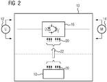
- FIG. 2 shows in this respect - also schematically simplified - the situation according to FIG. 1 in a serial transmission of the drive signals 20.
- the drive signals 20 are no longer individually, but transmitted via a here shown as a block arrow and otherwise known per se serial connection 22.
- the serial transmission 22 avoids otherwise required and expensive components for potential separation. Due to the high voltage gradients when switching the semiconductor switch T, however, shifting currents occur between the high-voltage and low-voltage sides of the drive control device 10. These shift currents can disturb the serial transmission of the drive signals 20 and cause the semiconductor switches T to be no longer properly controlled.
- FIG. 3 shows an embodiment of the drive control device 10, which can operate according to the method proposed here.
- the drive signals 20 are no longer transmitted themselves, but time information with regard to the times or the periodicity at which a drive signal is to be generated.
- the relevant, designated here as An Tavernsignalzeitif 24 information is determined by the drive logic 18.
- the drive signal times 24 are transmitted from the low-voltage side via the serial connection 22 to the high-voltage side and there to a drive circuit 26.
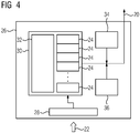
- the drive circuit 26 comprises a processing unit 34 (FIG. FIG. 4 ) in the form or in the manner of a microprocessor and a timer 36 ( FIG. 4 ), so that a comparison of the buffered An Tavernsignalzeit affect 24 with a respective current value of the timer 36 and based on a generation of drive signals 20 is possible.
- FIG. 4 shows the drive circuit 26 with further details. Thereafter, the drive circuit 26 includes an interface unit 28 for connecting a serial link 22. For buffering received via the serial link 22 Anêtsignalzeitticianen 24 a memory 30 is provided. In the memory 30, a control program 32, which determines the functionality of the drive circuit 26, is stored in addition to the respective control signal times 24 that have been buffered there. The control program 32 is executed during operation of the drive control device 10 or the drive circuit 26 by a processing unit 34 provided for this purpose. At this time, the processing unit 34 compares a value of the latched drive signal timings 24 with a time value supplied from a timer 36.
- the drive signal 20 belonging to the respective drive signal time 24 is generated.
- An assignment in this regard may be based on that the buffered An Kunststoffsignalzeitif 24 are stored in the memory 30 in a fixed order and upon agreement of stored in a first memory location of the memory 30 cached Anêtsignalzeitticians 24 with the instantaneous value of the timer 36 for driving a first semiconductor switch T provided Drive signal 20 is generated. This scheme can be continued for a second memory location and a drive signal 20 provided for driving a second semiconductor switch.
Description
Die Erfindung betrifft ein Verfahren zum Betrieb einer Antriebssteuerungseinrichtung und eine nach dem Verfahren arbeitende Antriebssteuerungseinrichtung sowie ein Computerprogramm zur Implementation des Verfahrens und damit auch eine Antriebssteuerungseinrichtung mit Mitteln zur Ausführung eines solchen Computerprogramms. Speziell betrifft die Erfindung ein Verfahren zum Betrieb einer Antriebssteuerungseinrichtung, wobei diese einen Wechselrichter aufweist und wobei dieser durch Ansteuersignale ansteuerbare Halbleiterschalter umfasst.The invention relates to a method for operating a drive control device and to a drive control device operating according to the method, and to a computer program for implementing the method, and thus also to a drive control device having means for executing such a computer program. Specifically, the invention relates to a method for operating a drive control device, wherein it has an inverter and wherein this comprises controllable by control signals semiconductor switch.
Derartige Antriebssteuerungseinrichtungen sind an sich bekannt. Die Wechselrichter erzeugen aufgrund der Ansteuerung durch die Ansteuersignale eine Ausgangsspannung mit variabler Frequenz und Spannung. Dadurch kann die Drehzahl und das Drehmoment z.B. eines Elektromotors als Last der Antriebssteuerungseinrichtung eingestellt und geregelt werden. Eine Ansteuerungselektronik zur Generierung der Ansteuersignale liegt auf einer Niederspannungsseite der Antriebssteuerungseinrichtung und der Wechselrichter demgegenüber auf einer Hochspannungsseite. Zwischen der Niederspannungs- und Hochspannungsseite besteht aus Sicherheitsgründen eine Potentialtrennung. Die Ansteuersignale müssen aber über diese Potentialtrennung hinweg übertragen werden. Dafür ist u.a. eine serielle Übertragung in Betracht gezogen worden. Nachteilig dabei ist aber, dass sich aufgrund hoher Spannungssteilheiten beim Schalten der Halbleiterschalter Verschiebeströme zwischen der Hoch- und Niederspannungsseite ergeben können. Diese stören die Signalübertragung und können dazu führen, dass die Halbleiterschalter nicht mehr richtig angesteuert werden können. Zur Lösung dieses Problems ist bisher in Betracht gezogen worden, die serielle Übertragung in ihrer Bandbreite soweit zu begrenzen, dass ein ausreichender Störabstand gegeben ist. Für evtl. noch auftretende Störungen werden Sicherheitsmaßnahmen, z.B. eine Telegrammwiederholung, implementiert, die sich aber letztlich negativ auf die Bandbreite auswirken. Alternativ kommt auch eine getrennte Übertragung der einzelnen Ansteuersignale in Betracht. Dies bedeutet aber, für jedes Ansteuersignal eine eigene Potentialtrennung zu implementieren, so dass diese Alternative sich als unflexibel und teuer darstellt.Such drive control devices are known per se. The inverters generate an output voltage of variable frequency and voltage due to the drive by the drive signals. As a result, the rotational speed and the torque, for example, of an electric motor can be set and regulated as a load of the drive control device. A control electronics for generating the drive signals is on a low voltage side of the drive control device and the inverter in contrast on a high voltage side. There is potential separation between the low voltage and high voltage side for safety reasons. However, the control signals must be transmitted across this potential separation. Among other things, a serial transmission has been considered. The disadvantage here is that due to high voltage gradients when switching the semiconductor switch shift currents between the high and low voltage side can result. These disturb the signal transmission and can lead to the fact that the semiconductor switches can no longer be controlled correctly. To solve this problem, it has hitherto been considered to limit the bandwidth of the serial transmission to such an extent that there is sufficient signal-to-noise ratio is. Security measures, such as telegram repetition, are implemented for any faults that still occur, but ultimately have a negative effect on the bandwidth. Alternatively, a separate transmission of the individual control signals comes into consideration. However, this means implementing a separate potential separation for each drive signal, so that this alternative presents itself as inflexible and expensive.
Aus der
Eine Aufgabe der Erfindung besteht entsprechend darin, ein weiteres Verfahren zum Betrieb einer Antriebssteuerungseinrichtung und eine nach dem Verfahren arbeitende Antriebssteuerungseinrichtung anzugeben, insbesondere ein Verfahren bei dem die oben genannten Nachteile im Hinblick auf Störungen der Übertragung der Ansteuersignalzeitpunkte von der Niederspannungs- zur Hochspannungsseite aufgrund von Schaltvorgängen des Halbleiterschalter vermieden oder zumindest hinsichtlich ihrer Auswirkungen reduziert werden.Accordingly, it is an object of the invention to provide another method for operating a drive control device and a drive control device operating according to the method, in particular a method in which the above-mentioned disadvantages with regard to disturbances in the transmission of the drive signal times from the low-voltage to the high-voltage side due to switching operations the semiconductor switch avoided or at least reduced in terms of their effects.
Diese Aufgabe wird erfindungsgemäß mit einem Verfahren mit den Merkmalen des Anspruchs 1 oder einer nach dem Verfahren abreitenden Vorrichtung gelöst. Dazu ist bei einem Verfahren zum Betrieb einer Antriebssteuerungseinrichtung mit einem. Wechselrichter mit durch Ansteuersignale ansteuerbaren Halbleiterschaltern, vorgesehen, dass eine Ansteuerlogik für jedes Ansteuersignal einen Ansteuersignalzeitpunkt ermittelt und die Ansteuersignalzeitpunkte im Betrieb von einer Niederspannungsseite der Antriebssteuerungseinrichtung mit der Ansteuerlogik zu einer Hochspannungsseite der Antriebssteuerungseinrichtung mit dem Wechselrichter übertragen werden, sowie dass die Übertragung der Ansteuersignalzeitpunkte während zwischen einzelnen Schaltpunkten der Halbleiterschalter verbleibenden Schaltpausen erfolgt und dass anhand der übertragenen Ansteuersignalzeitpunkte auf der Hochspannungsseite Ansteuersignale zur Ansteuerung der Halbleiterschalter generiert werden.This object is achieved according to the invention by a method having the features of claim 1 or a device passing through the method. This is in a method for operating a drive control device with a. Inverters with semiconductor switches which can be controlled by drive signals, provide that a drive logic determines a drive signal time for each drive signal and the drive signal times in operation from a low voltage side of the drive control device with the drive logic to a high voltage side of the drive control device be transmitted to the inverter, and that the transmission of Ansteuersignalzeitpunkte between switching points of the switching elements of the semiconductor switch remaining switching pauses takes place and that based on the transmitted Ansteuersignalzeitpunkte on the high voltage side driving signals for driving the semiconductor switches are generated.
Der Vorteil der Erfindung besteht darin, dass durch die Übertragung der Ansteuersignalzeitpunkte während der Schaltpausen der Halbleiterschalter Störungen aufgrund von Schaltvorgängen der Halbleiterschalter vermieden werden. Störungen aufgrund der oben genannten Verschiebeströme treten nämlich nur dann auf, wenn die Halbleiterschalter schalten. Wird der Zeitpunkt der Übertragung so gewählt, dass keine Halbleiterschalter schalten, können die Verschiebeströme die Übertragung der Ansteuersignalzeitpunkte nicht mehr stören.The advantage of the invention is that disturbances due to switching operations of the semiconductor switches are avoided by the transmission of the Ansteuersignalzeitpunkte during the switching pauses of the semiconductor switches. Disruptions due namely, the above-mentioned shift currents occur only when the semiconductor switches switch. If the time of transmission is chosen such that no semiconductor switches switch, the displacement currents can no longer disturb the transmission of the control signal instants.
Vorteilhafte Ausgestaltungen der Erfindung sind Gegenstand der Unteransprüche. Dabei verwendete Rückbeziehungen weisen auf die weitere Ausbildung des Gegenstandes des Hauptanspruches durch die Merkmale des jeweiligen Unteranspruches hin. Sie sind nicht als ein Verzicht auf die Erzielung eines selbständigen, gegenständlichen Schutzes für die Merkmalskombinationen der rückbezogenen Unteransprüche zu verstehen. Des Weiteren ist im Hinblick auf eine Auslegung der Ansprüche bei einer näheren Konkretisierung eines Merkmals in einem nachgeordneten Anspruch davon auszugehen, dass eine derartige Beschränkung in den jeweils vorangehenden Ansprüchen nicht vorhanden ist.Advantageous embodiments of the invention are the subject of the dependent claims. Here used backlinks indicate the further development of the subject matter of the main claim by the features of the respective subclaim. They should not be construed as a waiver of obtaining independent, objective protection for the feature combinations of the dependent claims. Furthermore, with a view to an interpretation of the claims in a closer specification of a feature in a subordinate claim, it is to be assumed that such a restriction does not exist in the respective preceding claims.
Eine Ermittlung einer Lage und Länge von Schaltpausen der Halbleiterschalter kann durch die Ansteuerlogik zusammen mit der Ermittlung der Ansteuersignalzeitpunkte erfolgen, denn mit den ermittelten Ansteuersignalzeitpunkten liegt eine Position der Schaltpunkte der Halbleiterschalter und ein dazwischen jeweils verbleibender Zeitraum und damit unmittelbar eine Information hinsichtlich Lage und Länge der Schaltpausen vor. Die Übertragung der Ansteuersignalzeitpunkte während der Schaltpausen der Halbleiterschalter kann damit in besonders günstiger Art und Weise durch die Ansteuerlogik durchgeführt oder initiiert werden.A determination of a position and length of switching pauses of the semiconductor switches can be done by the control logic together with the determination of the Ansteuersignalzeitpunkte, because with the determined Ansteuersignalzeitpunkten is a position of the switching points of the semiconductor switch and a period between each remaining period and thus immediately information regarding the position and length of Switching breaks before. The transmission of the Ansteuersignalzeitpunkte during the switching pauses of the semiconductor switches can thus be performed or initiated in a particularly favorable manner by the control logic.
Bei einer Ausführungsform des Verfahrens ist vorgesehen, dass die Ansteuersignalzeitpunkte von der Ansteuerlogik zu einer Ansteuerschaltung auf der Hochspannungsseite der Antriebssteuerungseinrichtung übermittelt werden, dass die Ansteuerschaltung die übermittelten Ansteuersignalzeitpunkte zwischenspeichert, dass die Ansteuerschaltung die zwischengespeicherten Ansteuersignalzeitpunkte mit dem Wert eines Zeitgebers, einer Uhr, Zählers oder dergleichen - im Folgenden zusammenfassend als Zeitgeber bezeichnet - vergleicht und dass in Abhängigkeit vom Ergebnis des Vergleichs durch die Ansteuerschaltung jeweils ein Ansteuersignal generiert wird. Dadurch, dass die übermittelten Ansteuersignalzeitpunkte durch die Ansteuerschaltung zwischengespeichert werden, ist eine zeitliche Entkopplung des Übertragungszeitpunkts der Ansteuersignalzeitpunkte von der Generierung eines oder mehrerer Ansteuersignale gegeben. Störanfällige Ansteuersignale brauchen nicht mehr direkt von der Niederspannungs- zur Hochspannungsseite übertragen werden und stattdessen erfolgt eine Übertragung von Ansteuersignalzeitpunkten als Basis für eine spätere und unabhängige Generierung von Ansteuersignalen.In one embodiment of the method, it is provided that the drive signal times are transmitted by the drive logic to a drive circuit on the high voltage side of the drive control device, that the drive circuit temporarily stores the transmitted drive signal times that the drive circuit stores the latched drive signal times with the value of a timer, a clock, counter or the like - hereinafter collectively referred to as a timer - compares and that in each case a drive signal is generated depending on the result of the comparison by the drive circuit. Characterized in that the transmitted Ansteuersignalzeitpunkte are temporarily stored by the drive circuit, a temporal decoupling of the transmission time of the Ansteuersignalzeitpunkte is given by the generation of one or more control signals. Fault-prone drive signals no longer need to be transferred directly from the low-voltage side to the high-voltage side, and instead a transmission of drive signal times is used as the basis for a later and independent generation of drive signals.
Wenn die Übertragung der Ansteuersignalzeitpunkte durch eine serielle Übertragung erfolgt, kann hinsichtlich der dafür notwendigen elektronischen Bauelemente auf bekannte und kostengünstige Elemente zurückgegriffen werden. Eine serielle Übertragung erlaubt zudem die Zusammenfassung mehrerer Ansteuersignalzeitpunkte zu einem Telegramm. Für ein Telegramm mit einem oder mehreren davon umfassten Ansteuersignalzeitpunkten können bekannte Verfahren zur Erkennung von Übertragungsfehlern eingesetzt werden, so dass bei einer erkannten Fehlerhaftigkeit einer Übertragung eine erneute Übertragung initiiert werden kann. Speziell kommt eine Absicherung der Datenübertragung mittels korrigierbarer Codes, z.B. Reed-Solomon-Codes oder dergleichen, in Betracht.If the transmission of the Ansteuersignalzeitpunkte done by a serial transmission, can be used with respect to the necessary electronic components on known and inexpensive elements. A serial transmission also allows the combination of several control signal times to form a telegram. For a telegram with one or more drive signal times comprised thereof, known methods for detecting transmission errors can be used so that a retransmission can be initiated if a fault of a transmission is detected. Specifically, protection of data transmission by means of correctable codes, e.g. Reed-Solomon codes or the like, into consideration.
Als Zeitpunkt zur Übertragung der Ansteuersignalzeitpunkte während der Schaltpausen der Halbleiterschalter kommt eine Übertragung eines Telegramms mit einer Mehrzahl von Ansteuersignalzeitpunkten in der Mitte eines Schaltintervalls der Halbleiterschalter in Betracht. Damit werden eine zeitliche Überschneidung der Übertragung mit den Schaltpunkten der Halbleiterschalter und damit ggf. einhergehende Störeinflüsse vermieden. Ein Schaltintervall ist der Zeitraum zwischen zwei Schaltpunkten eines Halbleiterschalters. Das Schaltintervall schließt also die Schaltpause ein. Je nach Länge des zur Übertragung zur Verfügung stehenden Schaltintervalls/Schaltpause der Halbleiterschalter kommt auch in Betracht, die serielle Übertragung in Form zweier Telegramme mit darauf aufgeteilten Ansteuersignalzeitpunkten durchzuführen, wobei eines der Telegramme am Anfang eines Schaltintervalls der Halbleiterschalter und das andere Telegramm in der Mitte des Schaltintervalls übertragen wird.As a time to transmit the Ansteuersignalzeitpunkte during the switching pauses of the semiconductor switch is a transmission of a telegram with a plurality of Ansteuersignalzeitpunkten in the middle of a switching interval of the semiconductor switch into consideration. In order for a temporal overlap of the transmission with the switching points of the semiconductor switches and thus possibly associated interference can be avoided. A switching interval is the period between two switching points of a semiconductor switch. The switching interval thus includes the switching pause. Depending on the length of the Transfer available switching interval / switching pause of the semiconductor switch is also considered to perform the serial transmission in the form of two telegrams with thereupon Ansteuersignalzeitpunkten, wherein one of the telegrams at the beginning of a switching interval of the semiconductor switch and the other telegram is transmitted in the middle of the switching interval.
Die oben genannte Aufgabe wird auch mit einer Antriebssteuerungseinrichtung gelöst, die nach dem Verfahren wie hier und im Folgenden beschrieben arbeitet und dazu Mittel zur Durchführung des Verfahrens umfasst. Das Verfahren und evtl. Ausgestaltungen ist bzw. sind dabei bevorzugt in Software implementiert. Die Erfindung ist damit einerseits auch ein Computerprogramm mit durch einen Computer ausführbaren Programmcodeanweisungen und andererseits ein Speichermedium mit einem derartigen Computerprogramm sowie schließlich auch eine Antriebssteuerungseinrichtung, in dessen Speicher als Mittel zur Durchführung des Verfahrens und seiner Ausgestaltungen ein solches Computerprogramm geladen oder ladbar ist.The above-mentioned object is also achieved with a drive control device which operates according to the method as described here and below and for this purpose comprises means for carrying out the method. The method and possibly embodiments are or are preferably implemented in software. The invention is thus on the one hand also a computer program with program code instructions executable by a computer and on the other hand a storage medium with such a computer program and finally also a drive control device in whose memory such a computer program is loaded or loadable as means for carrying out the method and its embodiments.
Nachfolgend wird ein Ausführungsbeispiel der Erfindung anhand der Zeichnung näher erläutert. Einander entsprechende Gegenstände oder Elemente sind in allen Figuren mit den gleichen Bezugszeichen versehen.An embodiment of the invention will be explained in more detail with reference to the drawing. Corresponding objects or elements are provided in all figures with the same reference numerals.
Es zeigen
- FIG 1
- eine Antriebssteuerungseinrichtung mit einem Wechselrichter auf einer Hochspannungsseite und einer Ansteuerlogik zur Generierung von Ansteuersignalen für den Wechselrichter auf einer Niederspannungsseite,
- FIG 2
- eine Antriebssteuerungseinrichtung gemäß
FIG 1 , bei der die Ansteuersignale über eine serielle Verbindung von der Niederspannungs- zur Hochspannungsseite übertragen werden, - FIG 3
- eine Antriebssteuerungseinrichtung gemäß
FIG 1 , bei der als Basis für die Ansteuersignale von der Niederspannungs- zur Hochspannungsseite über die serielle Verbindung Ansteuersignalzeitpunkte zu einer Ansteuerschaltung übertragen werden und - FIG 4
- Details der Ansteuerschaltung.
- FIG. 1
- a drive control device having an inverter on a high-voltage side and a drive logic for generating drive signals for the inverter on a low-voltage side,
- FIG. 2
- a drive control device according to
FIG. 1 in which the control signals are transmitted via a serial connection from the low-voltage side to the high-voltage side, - FIG. 3
- a drive control device according to
FIG. 1 in which, as the basis for the drive signals from the low-voltage side to the high-voltage side, drive signal times are transmitted to a drive circuit via the serial connection, and - FIG. 4
- Details of the drive circuit.
Für die Drehzahlregelung von z.B. Elektromotoren als Last 14 erzeugt der Wechselrichter 16 aus einer Zwischenkreisgleichspannung durch geeignetes Schalten der Halbleiterschalter T eine Ausgangsspannung mit variabler Frequenz und Spannung. Dadurch können die Drehzahl und das Drehmoment von Elektromotoren eingestellt und geregelt werden.For the speed control of e.g. Electric motors as a
Zur Ansteuerung der Halbleiterschalter T des Wechselrichters 16 ist eine Ansteuerlogik 18 vorgesehen. Die Ansteuerlogik 18 erzeugt für jeden Halbleiterschalter T ein Ansteuersignal 20, das zum jeweiligen Halbleiterschalter T übermittelt wird. Der Stromrichter 16 gehört zu einer Hochspannungsseite der Antriebssteuerungseinrichtung 10. Die Ansteuerlogik 18 gehört demgegenüber zu einer Niederspannungsseite der Antriebssteuerungseinrichtung 10. Hochspannungs- und Niederspannungsseite sind in der Darstellung durch eine gestrichelte Linie getrennt.For driving the semiconductor switches T of the
Zwischen der Hochspannungs- und Niederspannungsseite ist üblicherweise eine Potentialtrennung vorgesehen, um berührungsgefährliche Spannungen der Hochspannungsseite zu kapseln. Die Ansteuersignale 20 für die Halbleiterschalter T müssen über diese Potentialtrennung hinweg übertragen werden. Da im Betrieb eine Vielzahl von Ansteuersignalen 20 übertragen werden muss, geht der Trend zu einer seriellen Übertragung.Between the high voltage and low voltage side, a potential separation is usually provided to encapsulate hazardous voltages on the high voltage side. The drive signals 20 for the semiconductor switches T must be transmitted across this potential separation. Since in operation a plurality of drive signals 20 must be transmitted, the trend is for a serial transmission.
Claims (11)
- Method for operating a drive control device (10) having an inverter (16) comprising semiconductor switches which can be controlled by means of control signals (20),- wherein control logic (18) calculates a control signal time instant (24) for each control signal (20) and- wherein control signals (20) for controlling the semiconductor switches are generated on the high-voltage side on the basis of the control signal time instants (24),
characterised in that- the control signal time instants (24) are transmitted during operation from a low-voltage side of the drive control device (10) containing the control logic (18) to a high-voltage side of the drive control device (10) containing the inverter (16), and- the transmission of the control signal time instants (24) takes place during the switching pauses of the semiconductor switches. - Method according to claim 1, wherein a position and length of switching pauses of the semiconductor switches are determined by the control logic (18) in conjunction with the calculation of the control signal time instants (24).
- Method according to claim 1 or 2, wherein the control signal time instants (24) are transmitted by the control logic (18) to a control circuit (26) on the high-voltage side of the drive control device (10), wherein the control circuit (18) buffers the transmitted control signal time instants (24), wherein the control circuit (18) compares the buffered control signal time instants (24) with the value of a timer (36), and wherein a control signal (20) is generated in each case as a function of the result of the comparison.
- Method according to one of claims 1, 2 or 3, wherein the control signal time instants (24) are transmitted by means of a serial transmission.
- Method according to claim 4, wherein the serial transmission is effected in the form of precisely one telegram midway through a switching interval of the semiconductor switches.
- Method according to claim 4, wherein the serial transmission is effected in the form of precisely two telegrams having control signal time instants (24) divided between them, one of said telegrams being transmitted at the start of a switching interval of the semiconductor switches and one being transmitted midway through the switching interval.
- Drive control device comprising control logic (18) and a control circuit (26) communicatively connected thereto as means for executing the method according to one of claims 1 to 6, wherein control signal time instants (24) for controlling the semiconductor switches of the drive control device (10) can be calculated by means of the control logic (18) and switching pauses of the semiconductor switches determined on the basis thereof, wherein the control signal time instants (24) can be transmitted by the control logic (18) to the control circuit (26) during the switching pauses, and wherein control signals (20) for controlling the semiconductor switches can be generated by means of the control circuit (26) on the basis of the control signal time instants (24) and time information.
- Drive control device according to claim 7, comprising a memory (30), a processing unit (34) and a timer (36), wherein control signal time instants (24) which are or can be buffered in the memory (30) can be compared by means of the processing unit (34) with a time value supplied by the timer (36), and wherein a control signal (20) for controlling a semiconductor switch can be generated by the processing unit (34) as a function of the result of the comparison.
- Computer program having program code means for implementing a method according to one of claims 1 to 6.
- Data medium containing a computer program according to claim 9.
- Drive control device on which a computer program according to claim 9 is loaded.
Priority Applications (2)
| Application Number | Priority Date | Filing Date | Title |
|---|---|---|---|
| EP11166214.4A EP2525486B1 (en) | 2011-05-16 | 2011-05-16 | Method for operating a drive control device and drive control device operating by the method |
| US13/472,169 US8655460B2 (en) | 2011-05-16 | 2012-05-15 | Method for operating a drive control device and drive control device operating according to the method |
Applications Claiming Priority (1)
| Application Number | Priority Date | Filing Date | Title |
|---|---|---|---|
| EP11166214.4A EP2525486B1 (en) | 2011-05-16 | 2011-05-16 | Method for operating a drive control device and drive control device operating by the method |
Publications (2)
| Publication Number | Publication Date |
|---|---|
| EP2525486A1 EP2525486A1 (en) | 2012-11-21 |
| EP2525486B1 true EP2525486B1 (en) | 2018-10-17 |
Family
ID=45560589
Family Applications (1)
| Application Number | Title | Priority Date | Filing Date |
|---|---|---|---|
| EP11166214.4A Active EP2525486B1 (en) | 2011-05-16 | 2011-05-16 | Method for operating a drive control device and drive control device operating by the method |
Country Status (2)
| Country | Link |
|---|---|
| US (1) | US8655460B2 (en) |
| EP (1) | EP2525486B1 (en) |
Families Citing this family (3)
| Publication number | Priority date | Publication date | Assignee | Title |
|---|---|---|---|---|
| EP2775603B1 (en) * | 2013-03-05 | 2018-02-14 | Siemens Aktiengesellschaft | Method for operating a drive control device and drive control device operating by the method |
| EP2775605B1 (en) * | 2013-03-05 | 2018-02-07 | Siemens Aktiengesellschaft | Method for operating an inverter and inverter operating according to the method |
| EP3537240A1 (en) * | 2018-03-09 | 2019-09-11 | Siemens Aktiengesellschaft | Simplified adjustment of the parameters of a drive control |
Family Cites Families (17)
| Publication number | Priority date | Publication date | Assignee | Title |
|---|---|---|---|---|
| US5045988A (en) * | 1990-07-31 | 1991-09-03 | Eaton Corporation | Isolated adjustable frequency AC inverter control |
| KR0139982B1 (en) * | 1995-10-19 | 1998-07-15 | 김광호 | Digital pll synthesizer |
| US6028411A (en) * | 1997-01-29 | 2000-02-22 | Seagate Technology, Inc. | Circuit and method for modulating the commutation frequency of a disc drive motor |
| DE10063084B4 (en) | 2000-12-18 | 2009-12-03 | Siemens Ag | Power electronic circuit |
| EP1253490B1 (en) | 2001-04-25 | 2011-08-17 | Siemens Aktiengesellschaft | Method and device for secure speed monitoring |
| DE10203374A1 (en) | 2002-01-29 | 2003-08-07 | Siemens Ag | Method for holding a machine element and / or a load connected to it |
| DE10203375A1 (en) | 2002-01-29 | 2003-08-14 | Siemens Ag | Method for holding a machine element and / or a load connected to it |
| JP2004064505A (en) * | 2002-07-30 | 2004-02-26 | Renesas Technology Corp | Semiconductor integrated circuit device, wireless lan system, and automatic gain control system |
| DE10252109B4 (en) | 2002-11-08 | 2005-11-10 | Siemens Ag | Method for parameterization |
| DE10307999B4 (en) | 2003-02-25 | 2007-03-01 | Siemens Ag | Drive control device for a self-commutated power converter |
| DE10356515A1 (en) | 2003-12-03 | 2005-07-14 | Siemens Ag | drive system |
| DE102004019443B3 (en) | 2004-04-19 | 2005-08-11 | Siemens Ag | Power module has passive semiconductor chip arranged above active semiconductor chip on second film in close contact with surfaces of planar conducting tracks and first film of insulating material with planar conducting tracks |
| DE102005060354A1 (en) | 2005-12-16 | 2007-06-21 | Siemens Ag | Modular inverter system |
| DE102006025110A1 (en) | 2006-05-30 | 2007-12-06 | Siemens Ag | Inverter with a damping control loop |
| DE102007037850A1 (en) | 2007-08-10 | 2009-02-26 | Siemens Ag | drive system |
| US8159373B2 (en) * | 2009-07-28 | 2012-04-17 | Ecole Polytechnique Federale De Lausanne (Epfl) | Encoding and decoding information |
| JP5485390B2 (en) * | 2010-06-15 | 2014-05-07 | パナソニック株式会社 | Switching power supply device and semiconductor device |
-
2011
- 2011-05-16 EP EP11166214.4A patent/EP2525486B1/en active Active
-
2012
- 2012-05-15 US US13/472,169 patent/US8655460B2/en active Active
Non-Patent Citations (1)
| Title |
|---|
| None * |
Also Published As
| Publication number | Publication date |
|---|---|
| US8655460B2 (en) | 2014-02-18 |
| US20130131835A1 (en) | 2013-05-23 |
| EP2525486A1 (en) | 2012-11-21 |
Similar Documents
| Publication | Publication Date | Title |
|---|---|---|
| EP1389284B1 (en) | Safety switching module for testing the switching-off ability of a switching element in a safety switching module | |
| DE102015205627B4 (en) | Load drive device | |
| DE112017001344T5 (en) | Motor control device | |
| DE112014003605B4 (en) | Drive control device for an electric motor | |
| DE102009019792A1 (en) | Control system for safely operating at least one functional component | |
| EP2525486B1 (en) | Method for operating a drive control device and drive control device operating by the method | |
| DE102012101006A1 (en) | Electromechanical power steering apparatus for motor car, has electrically driven actuator whose executing units are connected with power electronic units | |
| EP3084949B1 (en) | Method for actuating inverters connected in parallel | |
| EP2774266B1 (en) | Method and apparatus for operating an electronically commutated electrical machine in the event of a fault | |
| DE10146523A1 (en) | Drive control device for a converter-fed, multi-phase motor | |
| EP3375087B1 (en) | Interface | |
| DE102016106547A1 (en) | SWITCHING DEVICE FOR AN ELECTRIC MOTOR, CONTROL DEVICE, STEERING SYSTEM | |
| DE102007017285A1 (en) | Method for monitoring three-phase machine, involves supplying input parameters of converter unit, where one of these input parameters is commutating angle of three-phase machine to be operated | |
| EP3584922B1 (en) | Compensation for delays in a high performance electronics system | |
| WO2004105206A1 (en) | Method and arrangement for monitoring a power output stage | |
| EP3285394B1 (en) | Electrical machine and method for operating an electrical machine and electrical machine | |
| DE112013006844T5 (en) | Signal transmission circuit and energy conversion device equipped therewith | |
| WO2007000285A1 (en) | Control system for a permanently-excited electric machine | |
| DE4024287A1 (en) | Vehicle control unit with microcomputer - feeds digital output signals back to single diagnostic input via decoupling elements to perform self-test | |
| EP2893603A2 (en) | Method for driving an active bridge rectifier in the event of load shedding, rectifier arrangement and computer program product | |
| EP3582388B1 (en) | Electric motor system | |
| EP2775605B1 (en) | Method for operating an inverter and inverter operating according to the method | |
| DE102016207259A1 (en) | Method and circuit arrangement for operating at least one semiconductor switch, method and power converter for operating an electrical machine | |
| DE102016211508A1 (en) | Method for controlling an electrical machine, control unit and control system for controlling an electrical machine | |
| WO2020212058A1 (en) | Method for controlling a multi-phase electric machine by means of space vector modulation, control device, and drive arrangement |
Legal Events
| Date | Code | Title | Description |
|---|---|---|---|
| PUAI | Public reference made under article 153(3) epc to a published international application that has entered the european phase |
Free format text: ORIGINAL CODE: 0009012 |
|
| AK | Designated contracting states |
Kind code of ref document: A1 Designated state(s): AL AT BE BG CH CY CZ DE DK EE ES FI FR GB GR HR HU IE IS IT LI LT LU LV MC MK MT NL NO PL PT RO RS SE SI SK SM TR |
|
| AX | Request for extension of the european patent |
Extension state: BA ME |
|
| RAP1 | Party data changed (applicant data changed or rights of an application transferred) |
Owner name: SIEMENS AKTIENGESELLSCHAFT |
|
| 17P | Request for examination filed |
Effective date: 20130419 |
|
| RAP1 | Party data changed (applicant data changed or rights of an application transferred) |
Owner name: SIEMENS AKTIENGESELLSCHAFT |
|
| GRAP | Despatch of communication of intention to grant a patent |
Free format text: ORIGINAL CODE: EPIDOSNIGR1 |
|
| STAA | Information on the status of an ep patent application or granted ep patent |
Free format text: STATUS: GRANT OF PATENT IS INTENDED |
|
| INTG | Intention to grant announced |
Effective date: 20180619 |
|
| GRAS | Grant fee paid |
Free format text: ORIGINAL CODE: EPIDOSNIGR3 |
|
| GRAA | (expected) grant |
Free format text: ORIGINAL CODE: 0009210 |
|
| STAA | Information on the status of an ep patent application or granted ep patent |
Free format text: STATUS: THE PATENT HAS BEEN GRANTED |
|
| AK | Designated contracting states |
Kind code of ref document: B1 Designated state(s): AL AT BE BG CH CY CZ DE DK EE ES FI FR GB GR HR HU IE IS IT LI LT LU LV MC MK MT NL NO PL PT RO RS SE SI SK SM TR |
|
| REG | Reference to a national code |
Ref country code: GB Ref legal event code: FG4D Free format text: NOT ENGLISH |
|
| REG | Reference to a national code |
Ref country code: CH Ref legal event code: EP |
|
| REG | Reference to a national code |
Ref country code: IE Ref legal event code: FG4D Free format text: LANGUAGE OF EP DOCUMENT: GERMAN |
|
| REG | Reference to a national code |
Ref country code: DE Ref legal event code: R096 Ref document number: 502011014856 Country of ref document: DE Ref country code: AT Ref legal event code: REF Ref document number: 1055161 Country of ref document: AT Kind code of ref document: T Effective date: 20181115 |
|
| REG | Reference to a national code |
Ref country code: CH Ref legal event code: NV Representative=s name: SIEMENS SCHWEIZ AG, CH |
|
| REG | Reference to a national code |
Ref country code: NL Ref legal event code: MP Effective date: 20181017 |
|
| REG | Reference to a national code |
Ref country code: LT Ref legal event code: MG4D |
|
| PG25 | Lapsed in a contracting state [announced via postgrant information from national office to epo] |
Ref country code: NL Free format text: LAPSE BECAUSE OF FAILURE TO SUBMIT A TRANSLATION OF THE DESCRIPTION OR TO PAY THE FEE WITHIN THE PRESCRIBED TIME-LIMIT Effective date: 20181017 |
|
| PG25 | Lapsed in a contracting state [announced via postgrant information from national office to epo] |
Ref country code: LV Free format text: LAPSE BECAUSE OF FAILURE TO SUBMIT A TRANSLATION OF THE DESCRIPTION OR TO PAY THE FEE WITHIN THE PRESCRIBED TIME-LIMIT Effective date: 20181017 Ref country code: HR Free format text: LAPSE BECAUSE OF FAILURE TO SUBMIT A TRANSLATION OF THE DESCRIPTION OR TO PAY THE FEE WITHIN THE PRESCRIBED TIME-LIMIT Effective date: 20181017 Ref country code: NO Free format text: LAPSE BECAUSE OF FAILURE TO SUBMIT A TRANSLATION OF THE DESCRIPTION OR TO PAY THE FEE WITHIN THE PRESCRIBED TIME-LIMIT Effective date: 20190117 Ref country code: FI Free format text: LAPSE BECAUSE OF FAILURE TO SUBMIT A TRANSLATION OF THE DESCRIPTION OR TO PAY THE FEE WITHIN THE PRESCRIBED TIME-LIMIT Effective date: 20181017 Ref country code: IS Free format text: LAPSE BECAUSE OF FAILURE TO SUBMIT A TRANSLATION OF THE DESCRIPTION OR TO PAY THE FEE WITHIN THE PRESCRIBED TIME-LIMIT Effective date: 20190217 Ref country code: BG Free format text: LAPSE BECAUSE OF FAILURE TO SUBMIT A TRANSLATION OF THE DESCRIPTION OR TO PAY THE FEE WITHIN THE PRESCRIBED TIME-LIMIT Effective date: 20190117 Ref country code: PL Free format text: LAPSE BECAUSE OF FAILURE TO SUBMIT A TRANSLATION OF THE DESCRIPTION OR TO PAY THE FEE WITHIN THE PRESCRIBED TIME-LIMIT Effective date: 20181017 Ref country code: ES Free format text: LAPSE BECAUSE OF FAILURE TO SUBMIT A TRANSLATION OF THE DESCRIPTION OR TO PAY THE FEE WITHIN THE PRESCRIBED TIME-LIMIT Effective date: 20181017 Ref country code: LT Free format text: LAPSE BECAUSE OF FAILURE TO SUBMIT A TRANSLATION OF THE DESCRIPTION OR TO PAY THE FEE WITHIN THE PRESCRIBED TIME-LIMIT Effective date: 20181017 |
|
| PG25 | Lapsed in a contracting state [announced via postgrant information from national office to epo] |
Ref country code: GR Free format text: LAPSE BECAUSE OF FAILURE TO SUBMIT A TRANSLATION OF THE DESCRIPTION OR TO PAY THE FEE WITHIN THE PRESCRIBED TIME-LIMIT Effective date: 20190118 Ref country code: PT Free format text: LAPSE BECAUSE OF FAILURE TO SUBMIT A TRANSLATION OF THE DESCRIPTION OR TO PAY THE FEE WITHIN THE PRESCRIBED TIME-LIMIT Effective date: 20190217 Ref country code: AL Free format text: LAPSE BECAUSE OF FAILURE TO SUBMIT A TRANSLATION OF THE DESCRIPTION OR TO PAY THE FEE WITHIN THE PRESCRIBED TIME-LIMIT Effective date: 20181017 Ref country code: SE Free format text: LAPSE BECAUSE OF FAILURE TO SUBMIT A TRANSLATION OF THE DESCRIPTION OR TO PAY THE FEE WITHIN THE PRESCRIBED TIME-LIMIT Effective date: 20181017 Ref country code: RS Free format text: LAPSE BECAUSE OF FAILURE TO SUBMIT A TRANSLATION OF THE DESCRIPTION OR TO PAY THE FEE WITHIN THE PRESCRIBED TIME-LIMIT Effective date: 20181017 |
|
| REG | Reference to a national code |
Ref country code: DE Ref legal event code: R097 Ref document number: 502011014856 Country of ref document: DE |
|
| PG25 | Lapsed in a contracting state [announced via postgrant information from national office to epo] |
Ref country code: CZ Free format text: LAPSE BECAUSE OF FAILURE TO SUBMIT A TRANSLATION OF THE DESCRIPTION OR TO PAY THE FEE WITHIN THE PRESCRIBED TIME-LIMIT Effective date: 20181017 Ref country code: DK Free format text: LAPSE BECAUSE OF FAILURE TO SUBMIT A TRANSLATION OF THE DESCRIPTION OR TO PAY THE FEE WITHIN THE PRESCRIBED TIME-LIMIT Effective date: 20181017 |
|
| PLBE | No opposition filed within time limit |
Free format text: ORIGINAL CODE: 0009261 |
|
| STAA | Information on the status of an ep patent application or granted ep patent |
Free format text: STATUS: NO OPPOSITION FILED WITHIN TIME LIMIT |
|
| PG25 | Lapsed in a contracting state [announced via postgrant information from national office to epo] |
Ref country code: RO Free format text: LAPSE BECAUSE OF FAILURE TO SUBMIT A TRANSLATION OF THE DESCRIPTION OR TO PAY THE FEE WITHIN THE PRESCRIBED TIME-LIMIT Effective date: 20181017 Ref country code: SK Free format text: LAPSE BECAUSE OF FAILURE TO SUBMIT A TRANSLATION OF THE DESCRIPTION OR TO PAY THE FEE WITHIN THE PRESCRIBED TIME-LIMIT Effective date: 20181017 Ref country code: SM Free format text: LAPSE BECAUSE OF FAILURE TO SUBMIT A TRANSLATION OF THE DESCRIPTION OR TO PAY THE FEE WITHIN THE PRESCRIBED TIME-LIMIT Effective date: 20181017 Ref country code: EE Free format text: LAPSE BECAUSE OF FAILURE TO SUBMIT A TRANSLATION OF THE DESCRIPTION OR TO PAY THE FEE WITHIN THE PRESCRIBED TIME-LIMIT Effective date: 20181017 |
|
| 26N | No opposition filed |
Effective date: 20190718 |
|
| PG25 | Lapsed in a contracting state [announced via postgrant information from national office to epo] |
Ref country code: SI Free format text: LAPSE BECAUSE OF FAILURE TO SUBMIT A TRANSLATION OF THE DESCRIPTION OR TO PAY THE FEE WITHIN THE PRESCRIBED TIME-LIMIT Effective date: 20181017 |
|
| GBPC | Gb: european patent ceased through non-payment of renewal fee |
Effective date: 20190516 |
|
| PG25 | Lapsed in a contracting state [announced via postgrant information from national office to epo] |
Ref country code: MC Free format text: LAPSE BECAUSE OF FAILURE TO SUBMIT A TRANSLATION OF THE DESCRIPTION OR TO PAY THE FEE WITHIN THE PRESCRIBED TIME-LIMIT Effective date: 20181017 |
|
| REG | Reference to a national code |
Ref country code: BE Ref legal event code: MM Effective date: 20190531 |
|
| PG25 | Lapsed in a contracting state [announced via postgrant information from national office to epo] |
Ref country code: LU Free format text: LAPSE BECAUSE OF NON-PAYMENT OF DUE FEES Effective date: 20190516 |
|
| PG25 | Lapsed in a contracting state [announced via postgrant information from national office to epo] |
Ref country code: TR Free format text: LAPSE BECAUSE OF FAILURE TO SUBMIT A TRANSLATION OF THE DESCRIPTION OR TO PAY THE FEE WITHIN THE PRESCRIBED TIME-LIMIT Effective date: 20181017 |
|
| PG25 | Lapsed in a contracting state [announced via postgrant information from national office to epo] |
Ref country code: GB Free format text: LAPSE BECAUSE OF NON-PAYMENT OF DUE FEES Effective date: 20190516 Ref country code: IE Free format text: LAPSE BECAUSE OF NON-PAYMENT OF DUE FEES Effective date: 20190516 |
|
| PG25 | Lapsed in a contracting state [announced via postgrant information from national office to epo] |
Ref country code: BE Free format text: LAPSE BECAUSE OF NON-PAYMENT OF DUE FEES Effective date: 20190531 |
|
| PGFP | Annual fee paid to national office [announced via postgrant information from national office to epo] |
Ref country code: CH Payment date: 20200803 Year of fee payment: 10 |
|
| PG25 | Lapsed in a contracting state [announced via postgrant information from national office to epo] |
Ref country code: CY Free format text: LAPSE BECAUSE OF FAILURE TO SUBMIT A TRANSLATION OF THE DESCRIPTION OR TO PAY THE FEE WITHIN THE PRESCRIBED TIME-LIMIT Effective date: 20181017 |
|
| PG25 | Lapsed in a contracting state [announced via postgrant information from national office to epo] |
Ref country code: HU Free format text: LAPSE BECAUSE OF FAILURE TO SUBMIT A TRANSLATION OF THE DESCRIPTION OR TO PAY THE FEE WITHIN THE PRESCRIBED TIME-LIMIT; INVALID AB INITIO Effective date: 20110516 Ref country code: MT Free format text: LAPSE BECAUSE OF FAILURE TO SUBMIT A TRANSLATION OF THE DESCRIPTION OR TO PAY THE FEE WITHIN THE PRESCRIBED TIME-LIMIT Effective date: 20181017 |
|
| PGFP | Annual fee paid to national office [announced via postgrant information from national office to epo] |
Ref country code: FR Payment date: 20210526 Year of fee payment: 11 |
|
| PGFP | Annual fee paid to national office [announced via postgrant information from national office to epo] |
Ref country code: AT Payment date: 20210412 Year of fee payment: 11 |
|
| REG | Reference to a national code |
Ref country code: CH Ref legal event code: PL |
|
| PG25 | Lapsed in a contracting state [announced via postgrant information from national office to epo] |
Ref country code: LI Free format text: LAPSE BECAUSE OF NON-PAYMENT OF DUE FEES Effective date: 20210531 Ref country code: CH Free format text: LAPSE BECAUSE OF NON-PAYMENT OF DUE FEES Effective date: 20210531 |
|
| PG25 | Lapsed in a contracting state [announced via postgrant information from national office to epo] |
Ref country code: MK Free format text: LAPSE BECAUSE OF FAILURE TO SUBMIT A TRANSLATION OF THE DESCRIPTION OR TO PAY THE FEE WITHIN THE PRESCRIBED TIME-LIMIT Effective date: 20181017 |
|
| REG | Reference to a national code |
Ref country code: AT Ref legal event code: MM01 Ref document number: 1055161 Country of ref document: AT Kind code of ref document: T Effective date: 20220516 |
|
| PG25 | Lapsed in a contracting state [announced via postgrant information from national office to epo] |
Ref country code: AT Free format text: LAPSE BECAUSE OF NON-PAYMENT OF DUE FEES Effective date: 20220516 |
|
| PG25 | Lapsed in a contracting state [announced via postgrant information from national office to epo] |
Ref country code: FR Free format text: LAPSE BECAUSE OF NON-PAYMENT OF DUE FEES Effective date: 20220531 |
|
| PGFP | Annual fee paid to national office [announced via postgrant information from national office to epo] |
Ref country code: IT Payment date: 20230523 Year of fee payment: 13 |
|
| PGFP | Annual fee paid to national office [announced via postgrant information from national office to epo] |
Ref country code: DE Payment date: 20230719 Year of fee payment: 13 |