EP2525409B1 - Graphenbasierter Transistor mit Kollektorsperrschicht mit gradierter Zusammensetzung - Google Patents
Graphenbasierter Transistor mit Kollektorsperrschicht mit gradierter Zusammensetzung Download PDFInfo
- Publication number
- EP2525409B1 EP2525409B1 EP11190486.8A EP11190486A EP2525409B1 EP 2525409 B1 EP2525409 B1 EP 2525409B1 EP 11190486 A EP11190486 A EP 11190486A EP 2525409 B1 EP2525409 B1 EP 2525409B1
- Authority
- EP
- European Patent Office
- Prior art keywords
- layer
- collector
- emitter
- base
- barrier layer
- Prior art date
- Legal status (The legal status is an assumption and is not a legal conclusion. Google has not performed a legal analysis and makes no representation as to the accuracy of the status listed.)
- Active
Links
Images





Classifications
-
- H—ELECTRICITY
- H10—SEMICONDUCTOR DEVICES; ELECTRIC SOLID-STATE DEVICES NOT OTHERWISE PROVIDED FOR
- H10D—INORGANIC ELECTRIC SEMICONDUCTOR DEVICES
- H10D10/00—Bipolar junction transistors [BJT]
- H10D10/80—Heterojunction BJTs
- H10D10/821—Vertical heterojunction BJTs
- H10D10/881—Resonant tunnelling transistors
-
- H—ELECTRICITY
- H10—SEMICONDUCTOR DEVICES; ELECTRIC SOLID-STATE DEVICES NOT OTHERWISE PROVIDED FOR
- H10D—INORGANIC ELECTRIC SEMICONDUCTOR DEVICES
- H10D48/00—Individual devices not covered by groups H10D1/00 - H10D44/00
- H10D48/30—Devices controlled by electric currents or voltages
- H10D48/32—Devices controlled by only the electric current supplied, or only the electric potential applied, to an electrode which does not carry the current to be rectified, amplified or switched
- H10D48/36—Unipolar devices
- H10D48/362—Unipolar transistors having ohmic electrodes on emitter-like, base-like, and collector-like regions, e.g. hot electron transistors [HET], metal base transistors [MBT], resonant tunnelling transistors [RTT], bulk barrier transistors [BBT], planar doped barrier transistors [PDBT] or charge injection transistors [CHINT]
-
- H—ELECTRICITY
- H10—SEMICONDUCTOR DEVICES; ELECTRIC SOLID-STATE DEVICES NOT OTHERWISE PROVIDED FOR
- H10D—INORGANIC ELECTRIC SEMICONDUCTOR DEVICES
- H10D62/00—Semiconductor bodies, or regions thereof, of devices having potential barriers
- H10D62/10—Shapes, relative sizes or dispositions of the regions of the semiconductor bodies; Shapes of the semiconductor bodies
- H10D62/13—Semiconductor regions connected to electrodes carrying current to be rectified, amplified or switched, e.g. source or drain regions
- H10D62/137—Collector regions of BJTs
-
- H—ELECTRICITY
- H10—SEMICONDUCTOR DEVICES; ELECTRIC SOLID-STATE DEVICES NOT OTHERWISE PROVIDED FOR
- H10D—INORGANIC ELECTRIC SEMICONDUCTOR DEVICES
- H10D62/00—Semiconductor bodies, or regions thereof, of devices having potential barriers
- H10D62/10—Shapes, relative sizes or dispositions of the regions of the semiconductor bodies; Shapes of the semiconductor bodies
- H10D62/13—Semiconductor regions connected to electrodes carrying current to be rectified, amplified or switched, e.g. source or drain regions
- H10D62/165—Tunnel injectors
-
- H—ELECTRICITY
- H10—SEMICONDUCTOR DEVICES; ELECTRIC SOLID-STATE DEVICES NOT OTHERWISE PROVIDED FOR
- H10D—INORGANIC ELECTRIC SEMICONDUCTOR DEVICES
- H10D62/00—Semiconductor bodies, or regions thereof, of devices having potential barriers
- H10D62/10—Shapes, relative sizes or dispositions of the regions of the semiconductor bodies; Shapes of the semiconductor bodies
- H10D62/17—Semiconductor regions connected to electrodes not carrying current to be rectified, amplified or switched, e.g. channel regions
- H10D62/177—Base regions of bipolar transistors, e.g. BJTs or IGBTs
-
- H—ELECTRICITY
- H10—SEMICONDUCTOR DEVICES; ELECTRIC SOLID-STATE DEVICES NOT OTHERWISE PROVIDED FOR
- H10D—INORGANIC ELECTRIC SEMICONDUCTOR DEVICES
- H10D62/00—Semiconductor bodies, or regions thereof, of devices having potential barriers
- H10D62/80—Semiconductor bodies, or regions thereof, of devices having potential barriers characterised by the materials
- H10D62/881—Semiconductor bodies, or regions thereof, of devices having potential barriers characterised by the materials being a two-dimensional material
- H10D62/882—Graphene
Definitions
- the present invention relates to a junction transistor, comprising an emitter layer, a collector layer, and a base layer that comprises a graphene layer, wherein an emitter barrier layer is arranged between the base layer and the emitter layer, and a collector barrier layer is arranged between the base and the collector.
- Carbon-based materials are considered as having a great potential to improve digital and radio frequency (RF) electronics.
- Graphene is a name given to a single layer of carbon atoms arranged in a honeycomb lattice, although also films built of few graphene sheets stacked one upon another are often referred to as graphene (or few-layer graphene) and shall also be considered as embodiments of a graphene layer herein.
- Single-layer graphene is a zero band gap semiconductor with outstanding material properties, such as charge carrier mobility of around 1.2x10 5 cm 2 /Vs at 240 K, high field electron velocity of 4x10 7 cm/s, sheet resistance as low as 125 ⁇ /sq (about 30 ⁇ /sq for four-layer films), and thickness of only 0.34 nm.
- a high-performance RF (radio frequency) junction transistor is known from WO 2010/072590 . Control of operation of such a transistor is performed by driving a tunnel junction, which allows a flow of charge carriers in one direction when subjected to an operation voltage.
- a junction transistor comprises an emitter layer, a collector layer, and a base layer that comprises a graphene layer, wherein an emitter barrier layer is arranged between the base layer and the emitter layer, and a collector barrier layer is arranged between the base and the collector layers and adjacent to the graphene layer, wherein the collector barrier layer is a compositionally graded material layer, which at an interface between the base layer and the collector barrier layer has a higher electron affinity than at an interface between the collector layer and the collector barrier layer.
- the collector barrier layer is preferably configured to avoid a current of charge carriers between the base layer and the collector layer in absence of a carrier injection from the emitter layer into the base layer.
- the junction transistor of the present invention achieves a particular band structure profile with a conduction-band profile defined by a conduction-band edge that defines a lower limit of energy of allowed states of electrons as a function of the position across the graphene layer and the collector barrier layer in a direction pointing form the base layer to the collector layer.
- the conduction-band profile has a step-like increase in energy at an interface between the graphene layer and the collector barrier layer and, in correspondence with the composition grading, a monotonous decrease of the lower conduction band edge with increasing distance from the base layer in the direction pointing from the base layer to the collector layer.
- the junction transistor of the present invention allows achieving a high collector current, low base currents and - in some embodiments - a high output power.
- the energy barrier is defined as defined above by the profile of the lower edge of the conduction band as a function of position across the graphene layer and the collector barrier layer.
- the energy barrier of the junction transistor of the present invention provides a high transparency to electrons when an operating voltage is applied to the transistor and allows avoiding the formation of a tunneling barrier for electrons, and, at least to a large extent, the occurrence of quantum reflection at the interface between the graphene layer and the collector barrier layer.
- a monotonous decrease of energy is to be understood in a mathematical sense, i.e., as a decreasing profile that may include a section with constant energy but must not contain a section with increasing energy.
- a compositionally graded material is to be understood as a composite material, in the present context a layer of a solid-state material, which may be defined by at least two material components that assume defined fractions of a unit quantity of the composite material. All fractions add up to 100 %, but the fractions of the individual components change as a function of position in a certain direction. In the present case, the direction points from the base layer to the collector layer.
- Non-restrictive examples of a compositionally graded material layer form a mixture or an alloy.
- a transistor of this kind may have a base layer that consists of the graphene layer, which in one embodiment has a thickness as low as one atomic layer.
- the collector barrier layer is a composite dielectric material, the electron affinity of which decreases linearly with increasing distance from the base layer. It is important to note that there is no implicit or mandatory correspondence whatsoever between the electron affinity and the dielectric constant.
- a dielectric constant of the compositionally graded material is in some embodiments nearly constant across the collector barrier layer.
- the dielectric constant of the collector barrier layer does decrease with increasing distance from the base layer in a direction pointing from the base to the collector. For instance, in a suitable profile the dielectric constant decreases from a value between 40 and 60 at an interface between the graphene layer and the collector barrier layer, to a value between 3 and 5 at an interface between the collector barrier layer and the collector.
- the collector barrier layer comprises a sublayer arranged adjacent to the collector layer and having an electron affinity that does not change with increasing distance from the base layer.
- the collector barrier layer comprises a silicon dioxide layer adjacent to the collector layer.
- silicon dioxide By using silicon dioxide, sufficient dielectric strength for a high collector voltage (10-20 V), as needed for good power performance, is assured. If a lower collector voltage is needed for specific application purposes, the SiO 2 sub-layer may be substituted by a constant-composition extension of a compositionally graded part of the collector barrier layer.
- the composition profile can be designed to provide the desired potential shape at the operation output voltage.
- the compositionally graded collector barrier layer may comprise a compositionally graded Si x Ti 1-x O 2 layer on the silicon dioxide layer and, as an option, a SrTiO 3 layer at the interface between the collector barrier layer and the base.
- the Si x Ti 1-x O 2 layer may be understood as a composite material comprising the components SiO 2 and TiO 2 at fractions varying in position. Another way of notation is (SiO 2 ) x (TiO 2 ) 1-x .
- the silicon dioxide layer is present, its thickness is preferably between 5 and 30, suitably between 10 and 30 nanometer, even more suitably between 15 and 20 nanometer.
- the compositionally graded Si x Ti 1-x O 2 layer suitably has thickness of between 10 and 90 nanometer, in some embodiments between 20 and 40 nanometer.
- the SrTiO 3 layer if present at all, has a thickness of between 0.5 and 3 nanometer, preferably about 1 nanometer. As mentioned, the SrTiO 3 layer may be omitted.
- the collector layer is made of silicon.
- the conduction band offset between Si and TiO 2 is about 0 to 0.4 eV, and between Si and SrTiO 3 is about 0 to 0.2 eV.
- An alignment of the tunneling barrier to the emitter material is possible by choosing TiN for the emitter layer. The alignment in this case is also good with respect to the Fermi level in graphene, which is roughly aligned with that of TiN and can be around 0.5 eV.
- the junction transistor has a collector barrier layer that comprises a Ta 2 O 5 layer at the interface between the collector barrier layer and the collector, and a compositionally graded Ta x Ti y O layer at the interface between the collector barrier layer and the base.
- the conduction band of Ta 2 O 5 is about 0.4 eV above the conduction band of TiO 2 .
- the emitter barrier layer must support high currents in the tunneling regime.
- the emitter barrier layer forms a rather low tunneling barrier, preferably in the range of 0.5 eV or less.
- the layer sequence of emitter layer and emitter barrier layer is formed by a metallic emitter layer and a thin dielectric layer.
- the dielectric layer has a thickness below 5 nanometer, in particular of about 3 nanometer.
- a potential disadvantage of this configuration is the presence of a high electric field in the emitter barrier layer.
- the emitter layer of one embodiment is a highly doped (degenerate) semiconductor layer and the emitter barrier layer is an epitaxial intrinsic or near-intrinsic semiconductor layer (n ++ -i junction) of a moderate thickness, such as for instance in the range between 20 and 50 nm, preferably between 25 and 35, suitably about 30 nanometer.
- the electric field in the emitter barrier layer is low under operation conditions.
- the barrier profile of the emitter barrier layer as a function of position in a direction pointing from the emitter layer to the base layer may be designed either by a doping or by composition grading of the nominally intrinsic part.
- barrier shape helps to achieve a good transconductance at the working point of the junction transistor, and at the same time maintain the base current sufficiently low.
- a potential disadvantage of this configuration is the increased thickness of the emitter barrier layer, which in turn increases the thickness of the device.
- the emitter barrier layer forms a tunneling barrier, which under operation at predefined base and collector voltages has an amount, i.e., a step height that is approximately the same, or not significantly lower than the barrier height of the collector barrier on the base side. This avoids a reflection of electrons from the collector barrier layer, which would otherwise result in the base leads collecting the reflected electrons.
- the first of the above-mentioned two alternative embodiments includes a metallic emitter layer that either comprises or consists of a titanium nitride layer.
- a suitable emitter barrier layer comprises, arranged adjacent to the titanium nitride layer, a layer of Si (001), Ge (001), GaAs, Ta 2 O 5 , or TiO 2 .
- Germanium has the advantage of lower effective mass for electrons (0.082, as compared to 0.19 for Si).
- GaAs has also a low effective mass for electrons (0.067), and in addition is a direct-gap semiconductor, which makes tunneling sufficiently efficient even through an amorphous ultrathin GaAs film.
- the second of the alternative embodiments for the layer sequence of emitter layer and emitter barrier layer includes in different alternative embodiments an Er 2 Ge 2 /Ge layer stack, a n ++ -Si(001)/i-Si(001) layer stack, a n ++ -Ge(001)/i-Ge(001) layer stack, or a n ++ -GaAs(001)/i-GaAs(001) layer stack, wherein the Ge, i-Si(001), i-Ge(001) or the i-GaAs(001) forms the respective emitter barrier layer and is arranged between the emitter layer and the base layer, preferably adjacent to the graphene layer.
- GaAs the emitter barrier on the base side increases. Alloying with AlAs is an option for optimization of the energy barrier profile formed by the emitter barrier layer.
- BN Boron nitride has shown a potential for providing a particularly suitable substrate for the fabrication of a graphene layer.
- BN provides advantageous dielectric properties.
- BN is provided with a thickness of between 1 and 10 monolayers.
- graphene base transistor (GBT) of the present invention graphene is not used as a high mobility channel as in a field-effect device, but instead as an extremely thin, low resistivity electrode.
- the GBT thus combines the concept of a hot electron transistor with the unique properties of graphene to result in a high frequency device, which has a potential to overcome the difficulties faced by graphene RF FETs.
- a graphene sheet used in a base layer of the GBT may in principle contain several carbon sheets.
- the ultimate thickness of graphene sheet will be a compromise between the graphene deposition technique and the quantum transmission coefficient for electrons travelling across the sheet.
- the device concept is based on a vertical arrangement of the transistor electrodes emitter, base, and collector.
- An emitter-base diode acts as an electron emitter injecting hot electrons across the base layer (graphene) into the conducting band of the collector barrier layer, which takes the form of an insulating layer placed between the base and the collector and in the following will also be referred to in short as BCl or BCl layer.
- BCl insulating layer placed between the base and the collector and in the following will also be referred to in short as BCl or BCl layer.
- the electrons leave the emitter by Fowler-Nordheim quantum tunnelling through an emitter barrier layer, which is allow referred to as emitter-base insulator, EBI layer or EBI.
- the BCl can be much thicker than the EBI, so that it may receive a sufficiently high collector voltage.
- the graphene base works as the control electrode (grid in a vacuum tube). Ballistic transport across the base is expected, so the transparency is limited only by quantum effects.
- the base resistance is very low, despite its extremely small thickness: in contrast to ultrathin metal films, graphene covers the insulator in form of a closed sheet, with no pinholes that would increase the resistivity and lateral scattering. This leads to a very high gain and extremely low base current.
- the BCI layer can be designed in such a way that significantly higher voltages can be applied between the base and the collector electrode than it is possible in common transistors based on silicon. This is advantageous for the power performance of the device.
- Electrons injected from the emitter should be transmitted across the BCl with as small hindrance as possible. In the ideal case, they should cross the BCl in a ballistic process. This is in some conflict with the requirement that, for good power performance, the BCl should withstand VBC voltages of the order of 10 V.
- BCI is designed to consist of two regions.
- the region described in Fig. 2a as "constant barrier” can be a common SiO 2 film, while the region described as “graded barrier” can be a silicate with the metal (e.g., Ti) content gradually increasing from zero at the SiO 2 boundary.
- the shape of the barrier can be designed in this way and optimized such that when the output voltage is applied ( Fig.
- the collector current is not dramatically affected by a tunnelling barrier and/or by quantum reflections and still there is no BCl breakdown hazard.
- the disadvantage of lower electron mobility in a silicate/silica BCl ( ⁇ SiO 2 ⁇ 20 cm 2 /Vs) compared to Si is compensated by a the possibility to use a thinner film: the breakdown voltage of SiO 2 is at E krit around 6 ⁇ 10 6 V/cm about two orders of magnitude higher than for Si.
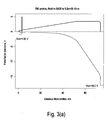
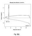
- Figure 3 shows realistic band diagrams of the BCI (a) designed for operation at a high output (collector) voltage, and (b) designed for operation at a moderate output voltage.
- Fig. 3 shows band profiles, also called band diagrams of the GBT with graded BCl.
- the emitter is on the right; the collector is on the left.
- a gray horizontal line at 0 V marks the Fermi level of the electrodes when no bias is applied, and the blue line is the potential in this case.
- the spike is the graphene layer.
- the emitter dielectric has the nominal barrier of 0.4 eV; the rounding on the emitter side is due to the image force.
- the collector dielectric consists of two parts: a graded part on the base side and a homogeneous part on the collector side.
- Fig: 3 (a) shows an embodiment of a High output voltage design.
- the BCI barrier at the interface to graphene is assumed to be 0.6 eV and the dielectric constant in the graded buffer is assumed to change linearly from 4 at the SiO 2 (collector) side to 50 at the TiO 2 (graphene) side.
- the red line is the potential when 1.0 V is applied between emitter and base, and 15 V is applied between emitter and collector.
- the electric field in the SiO 2 region remains below the critical field of 6 ⁇ 10 6 V/cm.
- Fig. 3 (b) shows an embodiment of a Moderate output voltage design.
- the emitter dielectric has the nominal barrier of 0.5 eV; the rounding on the emitter side is due to the image force.
- the collector dielectric consists of two parts.
- the BCl barrier is assumed to be 0.6 eV at the interface to graphene and 1.0 eV at the interface to the collector electrode.
- the dielectric constant in the graded buffer is assumed to be constant throughout the BEC.
- the red line is the potential when 1.0 V is applied between emitter and base, and 3.0 V is applied between emitter and collector.
- the device is expected to work in the THz regime.
- Tunnelling is known to be a very fast process, in the sense that the current response to of a tunnelling diode at a frequency as high as 2.5 THz can still resemble the dc curve.
- Emitter-base currents of the order of some mA and the EBI conductance of the order of some odd ten of mS can be possibly achieved with a 1 mm 2 device, meaning that the emitter-base injection can be fast enough.
- the transport across the rest of the structure can be ballistic, indicating that the characteristic delays there can be shorter than a picosecond.
- Figure 4 shows characteristics of a GBT with 3 nm EBI.
- the collector current (right panel) and the transconductance (left panel) are plotted Transfer as a function of the emitter-base voltage for the emitter-collector bias of 10 V.
- the horizontal grey line marks the current of 2 mA (right panel) and the transconductance of 1/13 S (left panel) estimated as needed for 100 GHz operation.
- the vertical grey line is drawn at 0.95 V (would be of advantage to circuit design if these target values are achieved at this voltage).
- the area of the device is assumed to be 1 ⁇ 2 .
- the target parameters are in this case reached at the base voltage of 1.05 V.
- Figure 4 illustrates the ability of GBT to work in the high frequency regime.
- Fig. 5 shows a band diagram illustrating the possibility to switch the GBT off by lowering the base bias from V on to V off .
- the base voltage By varying the base voltage, one modifies the tunnelling barrier. Since the collector dielectric can be much thicker than the emitter dielectric, the device can be designed for low off current.
- Fig. 6 shows a band diagram illustrating the origin of the collector current saturation of GBT at output voltages above V sat .
- the electrodes are indicated as E, B, and C.
- the graphene basis is marked symbolically by a grey vertical bar.
- the output voltage is below the saturation value (green)
- the collector current is limited by tunnelling under the collector dielectric and the current varies strongly with the collector bias.
- the output voltage is above the saturation value (red)
- the collector dielectric has little influence on the current and the output current dependence on the output voltage is weak.
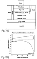
- Fig. 7 shows a schematic sketch of the physical design and the band diagram of an embodiment of a GBT according to the present invention.
- the blue line is the potential for electrons at zero voltage
- the red line is the potential for electrons at 1.7 eV between emitter and base and 16 V between emitter and collector.
- Flatband voltage of -0.55eV between a graphene base (work function about 4.6 eV) and an erbium germanide Er 2 Ge 3 emitter (work function about 4.05eV) and unpinned Ge/Er 2 Ge 3 interface are assumed.
- EBI barrier small effective mass of electrons in the EBI and high density of states in the emitter.
- the latter requirement strongly indicates that intrinsically metallic emitters should be used.
- the low-barrier requirement means in practice that the interface between the metal and the EBI should be unpinned and the work function of the emitter should be close to that of the EBI electron affinity. It seems that a workable solution can be: a Ge(001) film for the EBI and Er 2 Ge 3 emitter. It is known that the interface between germanium and a germanide electrode (and also silicon and a silicide electrode) can be efficiently unpinned by certain atoms, as sulphur, selenium, aluminium, or phosphorus.
- the work function of Er 2 Ge 3 (4.05 eV) matches the electron affinity of germanium (4.0 eV).
- the effective mass of electrons in the ⁇ minimum of germanium conduction band, i.e., for electrons travelling along the (001) direction, is 0.082.
- the Ge/emitter interface can be unpinned as efficiently as in the PrGe case (where the Schottky barrier to n-type Ge can be reduced to 0.16 eV), and that a Ge(001) EBI can be grown on the germanide (e.g., by an overgrowth process from Ge side wall)
- a GBT structure as sketched in Fig. 7 (a) .
- the corresponding band diagram is shown Fig. 7 (b) in the left panel.
- the dimensions are selected such that the device can work in THz regime, as estimated in Fig. 8 .
- the device is able to function at frequencies in the THz regime. Higher cut-off frequency is realized by shifting the working point to higher base bias, whereby a reduction of device area becomes possible: the bias of 1.3 V and area of 0.33 ⁇ m 2 is necessary for 2 THz operation, and 1 THz can be achieved already at 1.15 eV and with 0.5 ⁇ m 2 .
- the transparency of graphene to electrons may be the important factor limiting the high-frequency performance of the device.
- This transparency is in turn limited by the band structure of graphene: only the electrons penetrating the graphene under a significant angle, i.e., with a lateral momentum close enough to that of the Dirac point, see graphene as a narrow-gap insulator or even as a metal.
- graphene is an insulator with a wide band gap; in particular, for electrons entering the graphene nearly perpendicularly to the surface, the band gap is around 5 eV.
- a THz transistor Besides digital logic the most important application of a THz transistor will be its operation as a high-frequency linear small-signal amplifier.
- a small-signal amplifier receives and generates AC signals which are small compared to the transistor's DC bias voltages rsp. currents. Under the small-signal signalling regime the transistor is considered to be a linear amplifier with constant electrical parameters such as e. g. transconductance, R-parasitics, C-parasitics etc.
- transconductance e. g. transconductance, R-parasitics, C-parasitics etc.
- the transit frequency f T was calculated as an important figure of merit. This will allow to assess the potential of the GBT concept with state-of-the-art high-frequency transistors and yields transistor design rules for a maximum device cut-off frequency.
- Fig. 9a A simple low-frequency small-signal model of the transistor without R- and C-Parasitics is given in Fig. 9a .
- ⁇ 0 is much higher than 1 because most of the emitter current will transit through the very thin graphene base layer directly to the collector.
- the transconductance of the GBT is basically the differential conductance of its tunnel diode.
- Figure 9b shows a high-frequency small-signal transistor model of the GBT with metal emitter and metal collector. It includes all R- and C-parasitics of the GBT.
- R B denotes the resistance of the base contact as well as the graphene layer.
- R c represents the collector contact resistance while R E consists of the emitter contact resistance.
- a metal-oxide-silicon tunnel diode exhibits a plate capacitance between metal and semiconductor layer as well as an accumulation (or depletion) capacitance in silicon. If the silicon cathode is replaced by a metal cathode (emitter) there is no accumulation (or depletion) capacitance due to the conducting behaviour of the metal cathode (emitter).
- C ⁇ is a plate capacitance between base and emitter. Furthermore a substrate capacitance C s exists between emitter electrode and ground while C ⁇ is the base collector plate capacitance representing a metal-insulator-metal (MIM) capacitance.
- MIM metal-insulator-metal
- the equivalent circuit from Fig. 9c can be simplified with the assumption that R E and R c are so small that their contribution to DC and AC performance of the GBT is small. Neglecting R E' R c , we can redraw the equivalent circuit from Fig. 9a ) as shown in Fig. 9b ).
- Equation (5) represents a simple relation for a first order optimization w rt . maximum transistor speed.
- Small-signal transconductance g m rises with DC bias current I c .
- C ⁇ is proportional to the emitter area it makes sense to chose a high bias current I c with an as small as possible emitter area.
- the thickness t ox,BE of the base emitter SiO 2 layer has an influence on both the DC tunnel current as well as C ⁇ . It should be noted that while the tunnel current rises approximately proportional to t ox,BE 2 C ⁇ decreases with 1 / t ox, BE .
- f T is approximately proportional to t ox,BE so that a small t ox,BE is desirable.
Landscapes
- Bipolar Transistors (AREA)
Claims (13)
- Sperrschichttransistor, aufweisend, auf einem Substrat, eine Emitterschicht, eine Kollektorschicht, und eine Basisschicht, die eine Graphenschicht aufweist, wobei eine Emitterbarrierenschicht zwischen der Basisschicht und der Emitterschicht angeordnet ist, und wobei eine Kollektorbarrierenschicht zwischen der Basis- und der Kollektorschicht und angrenzend an die Graphenschicht angeordnet ist, dadurch gekennzeichnet, dass die Kollektorbarrierenschicht eine Materialschicht mit Zusammensetzungsgradient ist, die eine Elektronenaffinität hat, welche in einer von der Basisschicht zu der Kollektorschicht weisenden Richtung abnimmt.
- Sperrschichttransistor gemäß Anspruch 1, bei dem die Elektronenaffinität der ) Kollektorbarrierenschicht linear mit wachsendem Abstand von der Basisschicht abnimmt.
- Sperrschichttransistor gemäß einem der Ansprüche 1 oder 2, bei dem die Kollektorbarrierenschicht eine Unterschicht aufweist, die angrenzend an die Kollektorschicht angeordnet ist und eine Elektronenaffinität aufweist, die sich mit wachsendem Abstand von der Basisschicht nicht verändert.
- Sperrschichttransistor gemäß Anspruch 3, bei dem die Unterschicht eine Siliziumdioxidschicht an der Grenzfläche zwischen der Kollektorbarrierenschicht und dem Kollektor aufweist.
- Sperrschichttransistorgemäß Anspruch 4, bei dem die Kollektorbarrierenschicht weiterhin eine SiX'T1-x O2-Schicht zwischen der Siliziumdioxidschicht und der Basisschicht aufweist, wobei x mit zunehmendem Abstand von der Basisschicht zunimmt.
- Sperrschichttransistorgemäß Anspruch 4 oder 5, bei dem die Siliziumdioxidschicht eine Dicke zwischen 5 und 30 Nanometern hat, und die Si x Ti1-x O2 -Schicht, falls vorhanden, eine Dicke zwischen 10 und 90 Nanometern hat.
- Sperrschichttransistorgemäß einem der Ansprüche 1 bis 5, bei dem die Kollektorbarrierenschicht eine Ta2 O5-Schicht angrenzen an die Kollektorschicht und eine Ta Ti1-x O-Schicht angrenzend an die Basisschicht aufweist, wobei x mit zunehmendem Abstand von der Barrierenschicht zunimmt.
- Sperrschichttransistor gemäß einem der vorhergehenden Ansprüche, bei dem eine Dielektrizitätskonstante der Kollektorbarrierenschicht von einem Wert zwischen 40 und 60 an einer Grenzfläche zwischen der Graphenschicht und der Kollektorbarrierenschicht, bis auf einen Wert zwischen 3 und 5 an einer Grenzfläche zwischen der Kollektorbarrierenschicht und dem Kollektor abnimmt.
- Sperrschichttransistor gemäß einem der vorhergehenden Ansprüche, bei dem die Emitterschicht eine Titannitridschicht aufweist.
- Sperrschichttransistor gemäß einem der vorhergehenden Ansprüche, bei dem die Emitterschicht eine Er2 Ge2 -Schicht aufweist.
- Sperrschichttransistor gemäß Anspruch 9 oder 10, bei dem die Emitterbarrierenschicht angrenzend an die Titannitridschicht eine Schicht aus Si, insbesondere Si (001), Ge, insbesondere Ge (001), GaAs, Ta2 O5, oder TiO2 aufweist.
- Sperrschichttransistor gemäß einem der Ansprüche 1 bis 10, bei dem ein durch die Emitterschicht und die Emitterbarrierenschicht gebildeter Schichtstapel einen n++-Si(001)/i-Si(001)--Schichtstapel, einen n++-Ge(001)/i-Ge(001)-Schichtstapel oder einen n++-GaAs(001)/i-GaAs(001)-Schichtstapel, oder einen Er2 Ge2 /Ge- Schichtstapel aufweist.
- Sperrschichttransistorgemäß Anspruch 12, bei dem die Emitterbarrierenschicht zwischen 1 und 10 Monolagen aus BN aufweist, die angrenzend an die Graphenschicht angeordnet sind.
Priority Applications (2)
| Application Number | Priority Date | Filing Date | Title |
|---|---|---|---|
| EP11190486.8A EP2525409B1 (de) | 2011-05-17 | 2011-11-24 | Graphenbasierter Transistor mit Kollektorsperrschicht mit gradierter Zusammensetzung |
| US13/473,873 US9082809B2 (en) | 2011-05-17 | 2012-05-17 | Graphene base transistor having compositionally-graded collector barrier layer |
Applications Claiming Priority (2)
| Application Number | Priority Date | Filing Date | Title |
|---|---|---|---|
| EP11166332 | 2011-05-17 | ||
| EP11190486.8A EP2525409B1 (de) | 2011-05-17 | 2011-11-24 | Graphenbasierter Transistor mit Kollektorsperrschicht mit gradierter Zusammensetzung |
Publications (2)
| Publication Number | Publication Date |
|---|---|
| EP2525409A1 EP2525409A1 (de) | 2012-11-21 |
| EP2525409B1 true EP2525409B1 (de) | 2016-05-11 |
Family
ID=44992802
Family Applications (1)
| Application Number | Title | Priority Date | Filing Date |
|---|---|---|---|
| EP11190486.8A Active EP2525409B1 (de) | 2011-05-17 | 2011-11-24 | Graphenbasierter Transistor mit Kollektorsperrschicht mit gradierter Zusammensetzung |
Country Status (2)
| Country | Link |
|---|---|
| US (1) | US9082809B2 (de) |
| EP (1) | EP2525409B1 (de) |
Families Citing this family (11)
| Publication number | Priority date | Publication date | Assignee | Title |
|---|---|---|---|---|
| KR101920712B1 (ko) * | 2011-08-26 | 2018-11-22 | 삼성전자주식회사 | 튜너블 배리어를 구비한 그래핀 스위칭 소자 |
| EP2608267B1 (de) * | 2011-12-23 | 2019-02-27 | IHP GmbH-Innovations for High Performance Microelectronics / Leibniz-Institut für innovative Mikroelektronik | Transistor des Typs P mit Graphen-Basis |
| US9202945B2 (en) * | 2011-12-23 | 2015-12-01 | Nokia Technologies Oy | Graphene-based MIM diode and associated methods |
| KR102113255B1 (ko) * | 2013-02-22 | 2020-05-20 | 삼성전자주식회사 | 그래핀 적층 구조체의 제조방법, 및 그래핀 적층 구조체와 이를 구비하는 전기소자 |
| TWI493549B (zh) * | 2013-03-05 | 2015-07-21 | Nat Univ Tsing Hua | 電阻式隨機存取記憶體 |
| US9236432B2 (en) * | 2013-03-20 | 2016-01-12 | The United States Of America, As Represented By The Secretary Of The Navy | Graphene base transistor with reduced collector area |
| KR102059131B1 (ko) | 2013-04-05 | 2019-12-24 | 삼성전자주식회사 | 그래핀 소자 및 이의 제조 방법 |
| EP2808896B1 (de) | 2013-05-29 | 2016-05-18 | IHP GmbH-Innovations for High Performance Microelectronics / Leibniz-Institut für innovative Mikroelektronik | Transistor mit Basis aus Graphen und Verfahren zu seiner Herstellung |
| US9825712B2 (en) | 2013-12-06 | 2017-11-21 | Georgia Tech Research Corporation | Ultra massive MIMO communication in the terahertz band |
| US9397758B2 (en) | 2013-12-06 | 2016-07-19 | Georgia Tech Research Corporation | Graphene-based plasmonic nano-transceiver employing HEMT for terahertz band communication |
| CN103985741A (zh) * | 2014-06-06 | 2014-08-13 | 中国科学院上海微系统与信息技术研究所 | 一种基于ald的石墨烯基热电子晶体管及其制备方法 |
Family Cites Families (4)
| Publication number | Priority date | Publication date | Assignee | Title |
|---|---|---|---|---|
| EP0314836A1 (de) * | 1987-11-06 | 1989-05-10 | Max-Planck-Gesellschaft zur Förderung der Wissenschaften e.V. | Halbleiteranordnung, insbesondere Heiss-Elektronen-Transistor |
| DE102008055100A1 (de) | 2008-12-22 | 2010-07-01 | Ihp Gmbh - Innovations For High Performance Microelectronics / Leibniz-Institut Für Innovative Mikroelektronik | Unipolarer Hetero-Junction-Sperrschicht-Transistor |
| EP2221874A1 (de) * | 2009-02-24 | 2010-08-25 | S.a.r.l. FIRMUS | Verfahren zur Herstellung von nanoelektronischen Vorrichtungen aus 2D-Kohlenstoffkristallen wie Graphen und durch dieses Verfahren hergestellte Vorrichtungen |
| US8901536B2 (en) * | 2010-09-21 | 2014-12-02 | The United States Of America, As Represented By The Secretary Of The Navy | Transistor having graphene base |
-
2011
- 2011-11-24 EP EP11190486.8A patent/EP2525409B1/de active Active
-
2012
- 2012-05-17 US US13/473,873 patent/US9082809B2/en active Active
Also Published As
| Publication number | Publication date |
|---|---|
| EP2525409A1 (de) | 2012-11-21 |
| US20120292596A1 (en) | 2012-11-22 |
| US9082809B2 (en) | 2015-07-14 |
Similar Documents
| Publication | Publication Date | Title |
|---|---|---|
| US9082809B2 (en) | Graphene base transistor having compositionally-graded collector barrier layer | |
| EP2608267B1 (de) | Transistor des Typs P mit Graphen-Basis | |
| Joishi et al. | Effect of buffer iron doping on delta-doped β-Ga2O3 metal semiconductor field effect transistors | |
| US8901536B2 (en) | Transistor having graphene base | |
| US10158009B2 (en) | Method of making a graphene base transistor with reduced collector area | |
| Vaziri et al. | Going ballistic: Graphene hot electron transistors | |
| Yi et al. | Gate-tunable high mobility remote-doped InSb/In1− xAlxSb quantum well heterostructures | |
| US20200321443A1 (en) | Transistor with Multi-Metal Gate | |
| CN102054870A (zh) | 一种半导体结构及其形成方法 | |
| Panda et al. | Drain dielectric pocket engineering: its impact on the electrical performance of a hetero-structure tunnel FET | |
| Razzak et al. | RF operation in graded AlxGa1− xN (x= 0.65 to 0.82) channel transistors | |
| Venica et al. | Simulation of DC and RF performance of the graphene base transistor | |
| Sarker et al. | High performance semiconducting enriched carbon nanotube thin film transistors using metallic carbon nanotubes as electrodes | |
| Li et al. | Gate-controlled ZnO nanowires for field-emission device application | |
| Riederer et al. | Alternatives for Doping in Nanoscale Field‐Effect Transistors | |
| Kumar et al. | Performance analysis of charge plasma based five layered black phosphorus-silicon heterostructure tunnel field effect transistor | |
| Nah et al. | Realization of dual-gated Ge–SixGe1− x core-shell nanowire field effect transistors with highly doped source and drain | |
| Al-Dirini et al. | Graphene Self Switching Diodes with high rectification ratios | |
| Choi et al. | Enhancement mode p-channel SnO thin-film transistors with dual-gate structures | |
| Lee et al. | High-temperature threshold characteristics of a symmetrically graded InAlAs∕ InxGa1− xAs∕ GaAs metamorphic high electron mobility transistor | |
| Xia et al. | Materials and device engineering for high-performance gallium oxide devices | |
| Hsu et al. | Gate-metal formation-related kink effect and gate current on In0. 5Al0. 5As∕ In0. 5Ga0. 5As metamorphic high electron mobility transistor performance | |
| Xu et al. | Modulation-doped field-effect transistors with an 8-nm InGaAs/InAs/InGaAs quantum well | |
| Lee et al. | Temperature dependence of ballistic mobility in a metamorphic InGaAs/InAlAs high electron mobility transistor | |
| Chauhan et al. | Review of Tunnel Field Effect Transistors |
Legal Events
| Date | Code | Title | Description |
|---|---|---|---|
| PUAI | Public reference made under article 153(3) epc to a published international application that has entered the european phase |
Free format text: ORIGINAL CODE: 0009012 |
|
| AK | Designated contracting states |
Kind code of ref document: A1 Designated state(s): AL AT BE BG CH CY CZ DE DK EE ES FI FR GB GR HR HU IE IS IT LI LT LU LV MC MK MT NL NO PL PT RO RS SE SI SK SM TR |
|
| AX | Request for extension of the european patent |
Extension state: BA ME |
|
| 17P | Request for examination filed |
Effective date: 20130521 |
|
| GRAP | Despatch of communication of intention to grant a patent |
Free format text: ORIGINAL CODE: EPIDOSNIGR1 |
|
| INTG | Intention to grant announced |
Effective date: 20151118 |
|
| GRAS | Grant fee paid |
Free format text: ORIGINAL CODE: EPIDOSNIGR3 |
|
| GRAA | (expected) grant |
Free format text: ORIGINAL CODE: 0009210 |
|
| AK | Designated contracting states |
Kind code of ref document: B1 Designated state(s): AL AT BE BG CH CY CZ DE DK EE ES FI FR GB GR HR HU IE IS IT LI LT LU LV MC MK MT NL NO PL PT RO RS SE SI SK SM TR |
|
| REG | Reference to a national code |
Ref country code: GB Ref legal event code: FG4D |
|
| REG | Reference to a national code |
Ref country code: CH Ref legal event code: EP |
|
| REG | Reference to a national code |
Ref country code: AT Ref legal event code: REF Ref document number: 799269 Country of ref document: AT Kind code of ref document: T Effective date: 20160515 |
|
| REG | Reference to a national code |
Ref country code: IE Ref legal event code: FG4D |
|
| REG | Reference to a national code |
Ref country code: DE Ref legal event code: R096 Ref document number: 602011026366 Country of ref document: DE |
|
| REG | Reference to a national code |
Ref country code: LT Ref legal event code: MG4D |
|
| REG | Reference to a national code |
Ref country code: NL Ref legal event code: MP Effective date: 20160511 |
|
| PG25 | Lapsed in a contracting state [announced via postgrant information from national office to epo] |
Ref country code: NL Free format text: LAPSE BECAUSE OF FAILURE TO SUBMIT A TRANSLATION OF THE DESCRIPTION OR TO PAY THE FEE WITHIN THE PRESCRIBED TIME-LIMIT Effective date: 20160511 Ref country code: LT Free format text: LAPSE BECAUSE OF FAILURE TO SUBMIT A TRANSLATION OF THE DESCRIPTION OR TO PAY THE FEE WITHIN THE PRESCRIBED TIME-LIMIT Effective date: 20160511 Ref country code: NO Free format text: LAPSE BECAUSE OF FAILURE TO SUBMIT A TRANSLATION OF THE DESCRIPTION OR TO PAY THE FEE WITHIN THE PRESCRIBED TIME-LIMIT Effective date: 20160811 Ref country code: FI Free format text: LAPSE BECAUSE OF FAILURE TO SUBMIT A TRANSLATION OF THE DESCRIPTION OR TO PAY THE FEE WITHIN THE PRESCRIBED TIME-LIMIT Effective date: 20160511 |
|
| REG | Reference to a national code |
Ref country code: AT Ref legal event code: MK05 Ref document number: 799269 Country of ref document: AT Kind code of ref document: T Effective date: 20160511 |
|
| REG | Reference to a national code |
Ref country code: FR Ref legal event code: PLFP Year of fee payment: 6 |
|
| PG25 | Lapsed in a contracting state [announced via postgrant information from national office to epo] |
Ref country code: HR Free format text: LAPSE BECAUSE OF FAILURE TO SUBMIT A TRANSLATION OF THE DESCRIPTION OR TO PAY THE FEE WITHIN THE PRESCRIBED TIME-LIMIT Effective date: 20160511 Ref country code: RS Free format text: LAPSE BECAUSE OF FAILURE TO SUBMIT A TRANSLATION OF THE DESCRIPTION OR TO PAY THE FEE WITHIN THE PRESCRIBED TIME-LIMIT Effective date: 20160511 Ref country code: GR Free format text: LAPSE BECAUSE OF FAILURE TO SUBMIT A TRANSLATION OF THE DESCRIPTION OR TO PAY THE FEE WITHIN THE PRESCRIBED TIME-LIMIT Effective date: 20160812 Ref country code: SE Free format text: LAPSE BECAUSE OF FAILURE TO SUBMIT A TRANSLATION OF THE DESCRIPTION OR TO PAY THE FEE WITHIN THE PRESCRIBED TIME-LIMIT Effective date: 20160511 Ref country code: ES Free format text: LAPSE BECAUSE OF FAILURE TO SUBMIT A TRANSLATION OF THE DESCRIPTION OR TO PAY THE FEE WITHIN THE PRESCRIBED TIME-LIMIT Effective date: 20160511 Ref country code: LV Free format text: LAPSE BECAUSE OF FAILURE TO SUBMIT A TRANSLATION OF THE DESCRIPTION OR TO PAY THE FEE WITHIN THE PRESCRIBED TIME-LIMIT Effective date: 20160511 Ref country code: PT Free format text: LAPSE BECAUSE OF FAILURE TO SUBMIT A TRANSLATION OF THE DESCRIPTION OR TO PAY THE FEE WITHIN THE PRESCRIBED TIME-LIMIT Effective date: 20160912 |
|
| PG25 | Lapsed in a contracting state [announced via postgrant information from national office to epo] |
Ref country code: IT Free format text: LAPSE BECAUSE OF FAILURE TO SUBMIT A TRANSLATION OF THE DESCRIPTION OR TO PAY THE FEE WITHIN THE PRESCRIBED TIME-LIMIT Effective date: 20160511 |
|
| PG25 | Lapsed in a contracting state [announced via postgrant information from national office to epo] |
Ref country code: DK Free format text: LAPSE BECAUSE OF FAILURE TO SUBMIT A TRANSLATION OF THE DESCRIPTION OR TO PAY THE FEE WITHIN THE PRESCRIBED TIME-LIMIT Effective date: 20160511 Ref country code: SK Free format text: LAPSE BECAUSE OF FAILURE TO SUBMIT A TRANSLATION OF THE DESCRIPTION OR TO PAY THE FEE WITHIN THE PRESCRIBED TIME-LIMIT Effective date: 20160511 Ref country code: EE Free format text: LAPSE BECAUSE OF FAILURE TO SUBMIT A TRANSLATION OF THE DESCRIPTION OR TO PAY THE FEE WITHIN THE PRESCRIBED TIME-LIMIT Effective date: 20160511 Ref country code: CZ Free format text: LAPSE BECAUSE OF FAILURE TO SUBMIT A TRANSLATION OF THE DESCRIPTION OR TO PAY THE FEE WITHIN THE PRESCRIBED TIME-LIMIT Effective date: 20160511 Ref country code: RO Free format text: LAPSE BECAUSE OF FAILURE TO SUBMIT A TRANSLATION OF THE DESCRIPTION OR TO PAY THE FEE WITHIN THE PRESCRIBED TIME-LIMIT Effective date: 20160511 |
|
| REG | Reference to a national code |
Ref country code: DE Ref legal event code: R097 Ref document number: 602011026366 Country of ref document: DE |
|
| PG25 | Lapsed in a contracting state [announced via postgrant information from national office to epo] |
Ref country code: PL Free format text: LAPSE BECAUSE OF FAILURE TO SUBMIT A TRANSLATION OF THE DESCRIPTION OR TO PAY THE FEE WITHIN THE PRESCRIBED TIME-LIMIT Effective date: 20160511 Ref country code: AT Free format text: LAPSE BECAUSE OF FAILURE TO SUBMIT A TRANSLATION OF THE DESCRIPTION OR TO PAY THE FEE WITHIN THE PRESCRIBED TIME-LIMIT Effective date: 20160511 Ref country code: SM Free format text: LAPSE BECAUSE OF FAILURE TO SUBMIT A TRANSLATION OF THE DESCRIPTION OR TO PAY THE FEE WITHIN THE PRESCRIBED TIME-LIMIT Effective date: 20160511 Ref country code: BE Free format text: LAPSE BECAUSE OF FAILURE TO SUBMIT A TRANSLATION OF THE DESCRIPTION OR TO PAY THE FEE WITHIN THE PRESCRIBED TIME-LIMIT Effective date: 20160511 |
|
| PLBE | No opposition filed within time limit |
Free format text: ORIGINAL CODE: 0009261 |
|
| STAA | Information on the status of an ep patent application or granted ep patent |
Free format text: STATUS: NO OPPOSITION FILED WITHIN TIME LIMIT |
|
| 26N | No opposition filed |
Effective date: 20170214 |
|
| PG25 | Lapsed in a contracting state [announced via postgrant information from national office to epo] |
Ref country code: SI Free format text: LAPSE BECAUSE OF FAILURE TO SUBMIT A TRANSLATION OF THE DESCRIPTION OR TO PAY THE FEE WITHIN THE PRESCRIBED TIME-LIMIT Effective date: 20160511 |
|
| REG | Reference to a national code |
Ref country code: CH Ref legal event code: PL |
|
| PG25 | Lapsed in a contracting state [announced via postgrant information from national office to epo] |
Ref country code: LI Free format text: LAPSE BECAUSE OF NON-PAYMENT OF DUE FEES Effective date: 20161130 Ref country code: CH Free format text: LAPSE BECAUSE OF NON-PAYMENT OF DUE FEES Effective date: 20161130 |
|
| REG | Reference to a national code |
Ref country code: IE Ref legal event code: MM4A |
|
| PG25 | Lapsed in a contracting state [announced via postgrant information from national office to epo] |
Ref country code: LU Free format text: LAPSE BECAUSE OF NON-PAYMENT OF DUE FEES Effective date: 20161130 |
|
| REG | Reference to a national code |
Ref country code: FR Ref legal event code: PLFP Year of fee payment: 7 |
|
| PG25 | Lapsed in a contracting state [announced via postgrant information from national office to epo] |
Ref country code: IE Free format text: LAPSE BECAUSE OF NON-PAYMENT OF DUE FEES Effective date: 20161124 |
|
| PG25 | Lapsed in a contracting state [announced via postgrant information from national office to epo] |
Ref country code: HU Free format text: LAPSE BECAUSE OF FAILURE TO SUBMIT A TRANSLATION OF THE DESCRIPTION OR TO PAY THE FEE WITHIN THE PRESCRIBED TIME-LIMIT; INVALID AB INITIO Effective date: 20111124 Ref country code: CY Free format text: LAPSE BECAUSE OF FAILURE TO SUBMIT A TRANSLATION OF THE DESCRIPTION OR TO PAY THE FEE WITHIN THE PRESCRIBED TIME-LIMIT Effective date: 20160511 |
|
| PG25 | Lapsed in a contracting state [announced via postgrant information from national office to epo] |
Ref country code: IS Free format text: LAPSE BECAUSE OF FAILURE TO SUBMIT A TRANSLATION OF THE DESCRIPTION OR TO PAY THE FEE WITHIN THE PRESCRIBED TIME-LIMIT Effective date: 20160511 Ref country code: MK Free format text: LAPSE BECAUSE OF FAILURE TO SUBMIT A TRANSLATION OF THE DESCRIPTION OR TO PAY THE FEE WITHIN THE PRESCRIBED TIME-LIMIT Effective date: 20160511 Ref country code: MC Free format text: LAPSE BECAUSE OF FAILURE TO SUBMIT A TRANSLATION OF THE DESCRIPTION OR TO PAY THE FEE WITHIN THE PRESCRIBED TIME-LIMIT Effective date: 20160511 Ref country code: TR Free format text: LAPSE BECAUSE OF FAILURE TO SUBMIT A TRANSLATION OF THE DESCRIPTION OR TO PAY THE FEE WITHIN THE PRESCRIBED TIME-LIMIT Effective date: 20160511 |
|
| PG25 | Lapsed in a contracting state [announced via postgrant information from national office to epo] |
Ref country code: BG Free format text: LAPSE BECAUSE OF FAILURE TO SUBMIT A TRANSLATION OF THE DESCRIPTION OR TO PAY THE FEE WITHIN THE PRESCRIBED TIME-LIMIT Effective date: 20160511 |
|
| PG25 | Lapsed in a contracting state [announced via postgrant information from national office to epo] |
Ref country code: MT Free format text: LAPSE BECAUSE OF NON-PAYMENT OF DUE FEES Effective date: 20161124 |
|
| PG25 | Lapsed in a contracting state [announced via postgrant information from national office to epo] |
Ref country code: AL Free format text: LAPSE BECAUSE OF FAILURE TO SUBMIT A TRANSLATION OF THE DESCRIPTION OR TO PAY THE FEE WITHIN THE PRESCRIBED TIME-LIMIT Effective date: 20160511 |
|
| REG | Reference to a national code |
Ref country code: DE Ref legal event code: R079 Ref document number: 602011026366 Country of ref document: DE Free format text: PREVIOUS MAIN CLASS: H01L0029737000 Ipc: H10D0010800000 |
|
| PGFP | Annual fee paid to national office [announced via postgrant information from national office to epo] |
Ref country code: DE Payment date: 20241206 Year of fee payment: 14 |
|
| PGFP | Annual fee paid to national office [announced via postgrant information from national office to epo] |
Ref country code: GB Payment date: 20241121 Year of fee payment: 14 |
|
| PGFP | Annual fee paid to national office [announced via postgrant information from national office to epo] |
Ref country code: FR Payment date: 20241126 Year of fee payment: 14 |
|
| REG | Reference to a national code |
Ref country code: DE Ref legal event code: R082 Ref document number: 602011026366 Country of ref document: DE Representative=s name: EISENFUEHR SPEISER PATENTANWAELTE RECHTSANWAEL, DE |