EP2525251A1 - Liquid crystal display device - Google Patents
Liquid crystal display device Download PDFInfo
- Publication number
- EP2525251A1 EP2525251A1 EP10842983A EP10842983A EP2525251A1 EP 2525251 A1 EP2525251 A1 EP 2525251A1 EP 10842983 A EP10842983 A EP 10842983A EP 10842983 A EP10842983 A EP 10842983A EP 2525251 A1 EP2525251 A1 EP 2525251A1
- Authority
- EP
- European Patent Office
- Prior art keywords
- substrate
- liquid crystal
- alignment film
- display device
- sealing member
- Prior art date
- Legal status (The legal status is an assumption and is not a legal conclusion. Google has not performed a legal analysis and makes no representation as to the accuracy of the status listed.)
- Withdrawn
Links
- 239000004973 liquid crystal related substance Substances 0.000 title claims abstract description 57
- 239000000758 substrate Substances 0.000 claims abstract description 197
- 238000007789 sealing Methods 0.000 claims abstract description 59
- 239000000463 material Substances 0.000 claims abstract description 51
- 239000004020 conductor Substances 0.000 claims abstract description 9
- 239000010410 layer Substances 0.000 claims description 32
- 239000011229 interlayer Substances 0.000 claims description 20
- 230000000149 penetrating effect Effects 0.000 claims description 2
- 239000010408 film Substances 0.000 description 135
- 239000002245 particle Substances 0.000 description 16
- 239000011521 glass Substances 0.000 description 15
- 229920001721 polyimide Polymers 0.000 description 9
- 239000004642 Polyimide Substances 0.000 description 8
- 239000011248 coating agent Substances 0.000 description 6
- 238000000576 coating method Methods 0.000 description 6
- 239000003365 glass fiber Substances 0.000 description 6
- 238000002161 passivation Methods 0.000 description 6
- 238000007641 inkjet printing Methods 0.000 description 5
- 238000005516 engineering process Methods 0.000 description 4
- 239000011159 matrix material Substances 0.000 description 4
- 238000000206 photolithography Methods 0.000 description 4
- 239000011347 resin Substances 0.000 description 4
- 229920005989 resin Polymers 0.000 description 4
- 239000004925 Acrylic resin Substances 0.000 description 3
- 229920000178 Acrylic resin Polymers 0.000 description 3
- 239000011810 insulating material Substances 0.000 description 3
- 238000000034 method Methods 0.000 description 3
- 239000011368 organic material Substances 0.000 description 3
- VYPSYNLAJGMNEJ-UHFFFAOYSA-N Silicium dioxide Chemical compound O=[Si]=O VYPSYNLAJGMNEJ-UHFFFAOYSA-N 0.000 description 2
- 230000005540 biological transmission Effects 0.000 description 2
- 238000005530 etching Methods 0.000 description 2
- AMGQUBHHOARCQH-UHFFFAOYSA-N indium;oxotin Chemical compound [In].[Sn]=O AMGQUBHHOARCQH-UHFFFAOYSA-N 0.000 description 2
- 239000007788 liquid Substances 0.000 description 2
- 238000004519 manufacturing process Methods 0.000 description 2
- 239000004593 Epoxy Substances 0.000 description 1
- XUIMIQQOPSSXEZ-UHFFFAOYSA-N Silicon Chemical compound [Si] XUIMIQQOPSSXEZ-UHFFFAOYSA-N 0.000 description 1
- NIXOWILDQLNWCW-UHFFFAOYSA-N acrylic acid group Chemical group C(C=C)(=O)O NIXOWILDQLNWCW-UHFFFAOYSA-N 0.000 description 1
- 229910052681 coesite Inorganic materials 0.000 description 1
- 239000006258 conductive agent Substances 0.000 description 1
- 229910052906 cristobalite Inorganic materials 0.000 description 1
- 238000001312 dry etching Methods 0.000 description 1
- 230000000694 effects Effects 0.000 description 1
- 238000007647 flexography Methods 0.000 description 1
- -1 for example Substances 0.000 description 1
- 230000001681 protective effect Effects 0.000 description 1
- 229910052710 silicon Inorganic materials 0.000 description 1
- 239000010703 silicon Substances 0.000 description 1
- 239000000377 silicon dioxide Substances 0.000 description 1
- 239000002904 solvent Substances 0.000 description 1
- 238000004528 spin coating Methods 0.000 description 1
- 238000004544 sputter deposition Methods 0.000 description 1
- 229910052682 stishovite Inorganic materials 0.000 description 1
- 239000010409 thin film Substances 0.000 description 1
- 229910052905 tridymite Inorganic materials 0.000 description 1
- 238000001039 wet etching Methods 0.000 description 1
Images


Classifications
-
- G—PHYSICS
- G02—OPTICS
- G02F—OPTICAL DEVICES OR ARRANGEMENTS FOR THE CONTROL OF LIGHT BY MODIFICATION OF THE OPTICAL PROPERTIES OF THE MEDIA OF THE ELEMENTS INVOLVED THEREIN; NON-LINEAR OPTICS; FREQUENCY-CHANGING OF LIGHT; OPTICAL LOGIC ELEMENTS; OPTICAL ANALOGUE/DIGITAL CONVERTERS
- G02F1/00—Devices or arrangements for the control of the intensity, colour, phase, polarisation or direction of light arriving from an independent light source, e.g. switching, gating or modulating; Non-linear optics
- G02F1/01—Devices or arrangements for the control of the intensity, colour, phase, polarisation or direction of light arriving from an independent light source, e.g. switching, gating or modulating; Non-linear optics for the control of the intensity, phase, polarisation or colour
- G02F1/13—Devices or arrangements for the control of the intensity, colour, phase, polarisation or direction of light arriving from an independent light source, e.g. switching, gating or modulating; Non-linear optics for the control of the intensity, phase, polarisation or colour based on liquid crystals, e.g. single liquid crystal display cells
- G02F1/133—Constructional arrangements; Operation of liquid crystal cells; Circuit arrangements
- G02F1/1333—Constructional arrangements; Manufacturing methods
- G02F1/1339—Gaskets; Spacers; Sealing of cells
-
- G—PHYSICS
- G02—OPTICS
- G02F—OPTICAL DEVICES OR ARRANGEMENTS FOR THE CONTROL OF LIGHT BY MODIFICATION OF THE OPTICAL PROPERTIES OF THE MEDIA OF THE ELEMENTS INVOLVED THEREIN; NON-LINEAR OPTICS; FREQUENCY-CHANGING OF LIGHT; OPTICAL LOGIC ELEMENTS; OPTICAL ANALOGUE/DIGITAL CONVERTERS
- G02F1/00—Devices or arrangements for the control of the intensity, colour, phase, polarisation or direction of light arriving from an independent light source, e.g. switching, gating or modulating; Non-linear optics
- G02F1/01—Devices or arrangements for the control of the intensity, colour, phase, polarisation or direction of light arriving from an independent light source, e.g. switching, gating or modulating; Non-linear optics for the control of the intensity, phase, polarisation or colour
- G02F1/13—Devices or arrangements for the control of the intensity, colour, phase, polarisation or direction of light arriving from an independent light source, e.g. switching, gating or modulating; Non-linear optics for the control of the intensity, phase, polarisation or colour based on liquid crystals, e.g. single liquid crystal display cells
- G02F1/133—Constructional arrangements; Operation of liquid crystal cells; Circuit arrangements
- G02F1/1333—Constructional arrangements; Manufacturing methods
- G02F1/1337—Surface-induced orientation of the liquid crystal molecules, e.g. by alignment layers
- G02F1/13378—Surface-induced orientation of the liquid crystal molecules, e.g. by alignment layers by treatment of the surface, e.g. embossing, rubbing or light irradiation
- G02F1/133788—Surface-induced orientation of the liquid crystal molecules, e.g. by alignment layers by treatment of the surface, e.g. embossing, rubbing or light irradiation by light irradiation, e.g. linearly polarised light photo-polymerisation
-
- G—PHYSICS
- G02—OPTICS
- G02F—OPTICAL DEVICES OR ARRANGEMENTS FOR THE CONTROL OF LIGHT BY MODIFICATION OF THE OPTICAL PROPERTIES OF THE MEDIA OF THE ELEMENTS INVOLVED THEREIN; NON-LINEAR OPTICS; FREQUENCY-CHANGING OF LIGHT; OPTICAL LOGIC ELEMENTS; OPTICAL ANALOGUE/DIGITAL CONVERTERS
- G02F1/00—Devices or arrangements for the control of the intensity, colour, phase, polarisation or direction of light arriving from an independent light source, e.g. switching, gating or modulating; Non-linear optics
- G02F1/01—Devices or arrangements for the control of the intensity, colour, phase, polarisation or direction of light arriving from an independent light source, e.g. switching, gating or modulating; Non-linear optics for the control of the intensity, phase, polarisation or colour
- G02F1/13—Devices or arrangements for the control of the intensity, colour, phase, polarisation or direction of light arriving from an independent light source, e.g. switching, gating or modulating; Non-linear optics for the control of the intensity, phase, polarisation or colour based on liquid crystals, e.g. single liquid crystal display cells
- G02F1/133—Constructional arrangements; Operation of liquid crystal cells; Circuit arrangements
- G02F1/136—Liquid crystal cells structurally associated with a semi-conducting layer or substrate, e.g. cells forming part of an integrated circuit
- G02F1/1362—Active matrix addressed cells
- G02F1/136227—Through-hole connection of the pixel electrode to the active element through an insulation layer
-
- G—PHYSICS
- G02—OPTICS
- G02F—OPTICAL DEVICES OR ARRANGEMENTS FOR THE CONTROL OF LIGHT BY MODIFICATION OF THE OPTICAL PROPERTIES OF THE MEDIA OF THE ELEMENTS INVOLVED THEREIN; NON-LINEAR OPTICS; FREQUENCY-CHANGING OF LIGHT; OPTICAL LOGIC ELEMENTS; OPTICAL ANALOGUE/DIGITAL CONVERTERS
- G02F1/00—Devices or arrangements for the control of the intensity, colour, phase, polarisation or direction of light arriving from an independent light source, e.g. switching, gating or modulating; Non-linear optics
- G02F1/01—Devices or arrangements for the control of the intensity, colour, phase, polarisation or direction of light arriving from an independent light source, e.g. switching, gating or modulating; Non-linear optics for the control of the intensity, phase, polarisation or colour
- G02F1/13—Devices or arrangements for the control of the intensity, colour, phase, polarisation or direction of light arriving from an independent light source, e.g. switching, gating or modulating; Non-linear optics for the control of the intensity, phase, polarisation or colour based on liquid crystals, e.g. single liquid crystal display cells
- G02F1/133—Constructional arrangements; Operation of liquid crystal cells; Circuit arrangements
- G02F1/1333—Constructional arrangements; Manufacturing methods
- G02F1/1337—Surface-induced orientation of the liquid crystal molecules, e.g. by alignment layers
- G02F1/133776—Surface-induced orientation of the liquid crystal molecules, e.g. by alignment layers having structures locally influencing the alignment, e.g. unevenness
-
- G—PHYSICS
- G02—OPTICS
- G02F—OPTICAL DEVICES OR ARRANGEMENTS FOR THE CONTROL OF LIGHT BY MODIFICATION OF THE OPTICAL PROPERTIES OF THE MEDIA OF THE ELEMENTS INVOLVED THEREIN; NON-LINEAR OPTICS; FREQUENCY-CHANGING OF LIGHT; OPTICAL LOGIC ELEMENTS; OPTICAL ANALOGUE/DIGITAL CONVERTERS
- G02F1/00—Devices or arrangements for the control of the intensity, colour, phase, polarisation or direction of light arriving from an independent light source, e.g. switching, gating or modulating; Non-linear optics
- G02F1/01—Devices or arrangements for the control of the intensity, colour, phase, polarisation or direction of light arriving from an independent light source, e.g. switching, gating or modulating; Non-linear optics for the control of the intensity, phase, polarisation or colour
- G02F1/13—Devices or arrangements for the control of the intensity, colour, phase, polarisation or direction of light arriving from an independent light source, e.g. switching, gating or modulating; Non-linear optics for the control of the intensity, phase, polarisation or colour based on liquid crystals, e.g. single liquid crystal display cells
- G02F1/133—Constructional arrangements; Operation of liquid crystal cells; Circuit arrangements
- G02F1/1333—Constructional arrangements; Manufacturing methods
- G02F1/1339—Gaskets; Spacers; Sealing of cells
- G02F1/13398—Spacer materials; Spacer properties
Definitions
- the present invention relates to liquid crystal display devices, particularly to control of application of an alignment film.
- a liquid crystal display device includes a liquid crystal layer sealed between a pair of substrates.
- One of the paired substrates is a TFT substrate including a plurality of gate lines, a plurality of source lines, a plurality of pixel electrodes, a plurality of TFTs, etc.
- the other substrate is a counter substrate including a common electrode corresponding to the plurality of pixel electrodes.
- the liquid crystal layer is sealed with a frame-shaped sealing member surrounding the liquid crystal layer between the TFT substrate and the counter substrate.
- Each of the TFT substrate and the counter substrate includes an alignment film formed on a surface facing the liquid crystal layer to control orientation of liquid crystal molecules in the liquid crystal layer.
- the alignment film is made of a resin film, such as a polyimide film, and rubbing or photo-alignment has been performed on a surface thereof.
- the alignment film is formed by applying liquid polyimide on the surfaces of the TFT substrate and the counter substrate, and baking the liquid polyimide to cure.
- the polyimide may be applied by flexography, ink jet printing, etc.
- viscosity of an alignment film material such as polyimide needs to be relatively low so that drops of the alignment film material discharged toward the substrate and hit on the substrate can sufficiently spread on the surface of the substrate.
- the low viscosity alignment film material can smoothly spread on the surface of the substrate, and the alignment film material may unnecessarily spread to a region for forming the sealing member.
- Patent Documents 1 and 2 propose a technique of preventing the excessive spread of the alignment film material by forming a groove in the TFT substrate between the region for forming the sealing member and a pixel region which contributes to display so that the groove can hold the alignment film material.
- the groove When the groove is formed to hold the alignment film material therein as described in Patent Documents 1 and 2, the groove needs to be relatively wide to ensure a capacity for holding the alignment film material. As a result, a distance between the pixel region and the sealing member region increases, and a frame-shaped non-display region formed around the pixel region cannot easily be narrowed.
- a plurality of electrode portions are formed in the sealing member region, and the electrode portions are conducted to the common electrode on the counter substrate through conductive particles dispersed and mixed in the sealing member.
- FIG. 9 Referring to an enlarged plan view of FIG. 9 and an enlarged cross-sectional view of FIG. 10 , the structure of the sealing member region of the liquid crystal display device according to a related technology will be described below in connection with a technical problem to be solved by the present invention.
- a liquid crystal display device 100 includes a TFT substrate 101 and a counter substrate 102 facing each other as shown in FIG. 10 .
- a first electrode 103 and an interlayer insulating film 104 covering the first electrode are formed in a sealing member region for forming a sealing member on the TFT substrate 101.
- An opening 105 is formed in the interlayer insulating film 104 to penetrate the interlayer insulating film 104 to reach part the first electrode 103.
- the opening 105 is rectangular when viewed in a direction normal to the substrate as shown in FIG. 9 .
- a second electrode 106 is formed on the TFT substrate 101 to directly cover a surface of the interlayer insulating film 104, an inner wall surface of the opening 105, and the first electrode 103 exposed in the opening 105. Thus, the second electrode 106 is electrically connected to the first electrode 103.
- the second electrode 106 may be made of a transparent conductive film, such as an indium tin oxide (ITO) film. Unlike the TFT substrates of Patent Documents 1 and 2, the TFT substrate 101 is not provided with the groove.
- An alignment film 107 is formed on the interlayer insulating film 104 to cover the second electrode 106.
- the alignment film 107 is formed by spreading a low viscosity alignment film material from a pixel region (not shown) in an upward direction in FIG. 9 to cover the second electrode 106 and surround the opening 105.
- a common electrode 108 made of ITO etc. is formed on a surface of the counter substrate 102 facing the TFT substrate 101. Part of the common electrode 108 faces the second electrode 106.
- a sealing member 110 in which a plurality of conductive particles 109 are dispersed is provided between the counter substrate 102 and the TFT substrate 101. The conductive particles 109 are conducted with the common electrode 108.
- the alignment film 107 which is an insulating film, extends to the sealing member region to cover the second electrode 106, the alignment film 107 which is present between the second electrode 106 and the conductive particles 109 may inhibit conduction between the second electrode 106 and the common electrode 108 through the conductive particles 109.
- the present invention is concerned with narrowing a non-display region of a liquid crystal display device as much as possible, while ensuring electrical connection between a pair of substrates.
- the present invention is directed to a liquid crystal display device including: a first substrate; a second substrate facing the first substrate; a liquid crystal layer provided between the first substrate and the second substrate; and a sealing member provided between the first substrate and the second substrate to surround and seal the liquid crystal layer.
- Each of the first substrate and the second substrate includes a pixel region as a display region, a frame region as a non-display region which surrounds the pixel region and includes a sealing member region for forming the sealing member, alignment films, each extending from the pixel region to the sealing member region, are formed on a surface of the first substrate facing the liquid crystal layer and a surface of the second substrate facing the liquid crystal layer, respectively, by curing an alignment film material having fluidity, electrode portions are formed in the sealing member regions of the first substrate and the second substrate, respectively, so that the electrode portions are electrically connected to each other through a conductive material, and a control structure is formed at least between the electrode portion and the pixel region on at least one of the first substrate and the second substrate to control a flow of the alignment film material before curing so that at least part of the electrode portion is exposed from the alignment film.
- the alignment film before curing spreads from the pixel region to the sealing member region.
- the flow of the alignment film material which reached the sealing member region is controlled by the control structure, and at least part of the electrode portion is not covered with the alignment film, and is kept exposed.
- the part of the electrode portion and the conductive material are electrically connected because the alignment film is not present therebetween.
- the electrode portion on the first substrate and the electrode portion on the second substrate can electrically be connected through the conductive material.
- the frame region can greatly be narrowed, and the electrical connection between the first and second substrates can be ensured.
- the electrode portion on the first substrate and the electrode portion on the second substrate can electrically be connected through the conductive material even when the groove for holding the alignment film material is not provided between the pixel region and the sealing member region.
- the frame region can greatly be narrowed, and the electrical connection between the first and second substrates can be ensured.
- FIGS. 1-4 show a first embodiment of the present invention.
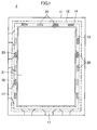
- FIG. 1 is a plan view showing a schematic structure of a TFT substrate 11 of the first embodiment.
- FIG. 2 is an enlarged plan view showing the vicinity of a pad 20 on the TFT substrate 11 of the first embodiment.
- FIG. 3 is a plan view showing an alignment film material 24 flowing toward the pad 20 on the TFT substrate 11 of the first embodiment.
- FIG. 4 is an enlarged cross-sectional view showing a cross-sectional structure of a liquid crystal display device 1 of the first embodiment.
- the liquid crystal display device 1 includes, as shown in FIGS. 1 and 4 , a TFT substrate 11 as a first substrate, a counter substrate 12 as a second substrate facing the TFT substrate 11, and a liquid crystal layer 13 provided between the TFT substrate 11 and the counter substrate 12.
- the liquid crystal display device 1 further includes a sealing member 14 provided between the TFT substrate 11 and the counter substrate 12 to surround and seal the liquid crystal layer 13.
- the sealing member 14 is substantially in the form of a rectangular frame as shown in FIG. 1 , and is made of a UV/thermally curable resin, such as an epoxy-based resin, in which a plurality of conductive particles 29 as a conductive material and glass fibers 30 are dispersed and mixed.
- An outer diameter of the conductive particle 29 is about 5 ⁇ m, and a diameter of the glass fiber 30 is about 4 ⁇ m.
- a line width of the sealing member 14 is about 0.5 mm, for example.
- FIGS. 2 and 3 only a single conductive particle 29 is shown, and the other conductive agents are not shown for easy description.
- Each of the TFT substrate 11 and the counter substrate 12 has a pixel region 31 as a display region, and a frame region 32 as a non-display region surrounding the pixel region 31.
- the frame region 32 includes a sealing member region 34 (a region for forming the sealing member 14) provided with a predetermined distance from the pixel region 31.
- Alignment films 23, each extending from the pixel region 31 to the sealing member region 14, are formed on a surface of the TFT substrate 11 facing the liquid crystal layer 13 and a surface of the counter substrate 12 facing the liquid crystal layer 13, respectively, by curing an alignment film material 24 having fluidity.
- the alignment film 23 is made of a resin material such as polyimide, and controls initial orientation of liquid crystal molecules in the liquid crystal layer 13.
- the alignment film material 24 has a viscosity reduced by adding a solvent to polyimide etc.
- the alignment film material 24 may be, for example, a vertical alignment film material having a viscosity of 6.5 mPa ⁇ s manufactured by JSR Corporation.
- the counter substrate 12 has a glass substrate 22 as a support substrate as shown in FIG. 4 .
- a common electrode 26 as an electrode portion which is made of a transparent conductive film, such as an ITO film, and has a thickness of about 100 nm is formed on a surface of the glass substrate 22 facing the TFT substrate 11.
- the common electrode 26 has a thickness of about 100 nm.
- a plurality of pixels are arranged in a matrix pattern in the pixel region 31 of the TFT substrate 11.
- a pixel electrode (not shown) made of a transparent conductive film, such as an indium tin oxide (ITO) film, is formed in each of the pixels.
- a thin-film transistor (TFT, not shown) as a switching element connected to the pixel electrode is formed in each of the pixels.
- Gate lines (not shown) and source lines (not shown) connected to the TFTs are formed on the TFT substrate 11.
- the TFT substrate 11 has a glass substrate 21 as a support substrate as shown in FIG. 4 .
- a plurality of gate lines and lower electrodes 40 are formed on a surface of the glass substrate 21 facing the counter substrate 12.
- the lower electrodes 40 are arranged at predetermined intervals in the sealing member region 34, and are made of the same material as the gate lines.
- the lower electrode 40 is made of a 100 nm thick Ti film, a 300 nm thick Al film stacked on the Ti film, and a 50 nm thick Ti film stacked on the Al film.
- a plurality of lead lines 17 made of the same material as the gate lines are formed in the frame region 32 on the glass substrate 21. Some of the lead lines 17 are connected to the lower electrodes 40. A line width of the lead line 17 is about 10 ⁇ m.
- a gate insulating film 41 is formed on the surface of the glass substrate 21 to cover the gate lines and the lower electrodes 40 as shown in FIG. 4 .
- the gate insulating film 41 is made of an oxide film, such as a SiO 2 film, and has a thickness of about 0.4 ⁇ m.
- a passivation film 42 as a protective film is formed on a surface of the gate insulating film 41.
- the passivation film 42 is made of an inorganic film, such as a SiN film, and has a thickness of about 0.25 ⁇ m.
- An interlayer insulating film 43 is formed on a surface of the passivation film 42 to cover the lower electrodes 40, etc.
- the interlayer insulating film 43 is made of a photosetting acrylic resin, for example, and has a thickness of about 2.5 ⁇ m.
- the pads 20 have a thickness of about 100 nm, and are arranged at predetermined intervals on the sealing member 14 as shown in FIG. 1 .
- the pads 20 are electrically connected to the common electrode 26 on the counter substrate 12 through the conductive particles 29 in the sealing member 14.
- the pads 20 are arranged to face the lower electrodes 40, respectively.
- An opening 44 in the form of a slit is formed in the interlayer insulating film 43, the passivation film 42, and the gate insulating film 41 to expose the lower electrode 40.
- each of the pads 20 is formed on the surface of the interlayer insulating film 43 and an inner surface of the opening 44.
- each of the pads 20 is electrically connected to the lower electrode 40 facing the pad 20 through the opening 44.
- a control structure 60 made of the recessed groove 45 is formed in the TFT substrate 11 of the first embodiment.
- the control structure 60 is arranged at least between the pad 20 and the pixel region 31, and controls the flow of the alignment film material 24 before curing so that at least part of the pad 20 is exposed from the alignment film 23.
- the control structure 60 of the present embodiment is made of a rectangular ring-shaped recessed groove 45 which covers at least part of the pad 20. Thus, part of the pad 20 surrounded by the rectangular ring-shaped recessed groove 45 is exposed from the alignment film 23.
- the recessed groove 45 has an inclined part 46 constituting an inner wall surface of the recessed groove 45, and part of the inclined part 46 is covered with the alignment film 23.
- the inclined part 46 has a round convex surface forming a rim of the recessed groove 45, and supports an edge of the alignment film 23.
- the alignment film 23 is not formed inside the recessed groove 45, and a bottom surface of the recessed groove 45 is exposed from the alignment film 23.
- the pad 20 has a short side of about 500 ⁇ m, and a long side of about 3140 ⁇ m.
- a line width of the recessed groove 45 is about 50 ⁇ m, and a distance between an outer edge of the recessed groove 45 and an outer edge of the pad 20 is about 20 ⁇ m.
- part of the pad 20 having a short side of about 360 ⁇ m and a long side of about 3000 ⁇ m inside the recessed groove 45 is exposed from the alignment film 23.
- the sealing member 14 is formed on the surface of the interlayer insulating film 43 in the sealing member region 34 to cover the pad 20 and the recessed groove 45.
- the conductive particles 29 in the sealing member 14 are sandwiched between the pad 20 exposed from the alignment film 23 and the common electrode 26 of the counter substrate 12, thereby electrically connecting the pad 20 and the common electrode 26.
- the liquid crystal display device 1 is fabricated by forming the frame-shaped sealing member 14 on the TFT substrate 11 or the counter substrate 12, dropping liquid crystal inside the sealing member 14, and bonding the TFT substrate 11 and the counter substrate 12.
- lower electrodes 40 are formed simultaneously with gate lines (not shown) on a surface of a glass substrate 21 which is a transparent substrate. Then, a gate insulating film 41, a silicon film (i layer, n+ phase, not shown), source lines (not shown), and a passivation film 42 are formed to cover the lower electrodes and the gate lines. Then, an interlayer insulating film 43 is formed to cover the TFTs etc.
- the interlayer insulating film 43 can be made of a photosensitive organic material such as a photosetting acrylic region, or a non-photosensitive insulating film.
- a photosensitive organic material such as a photosetting acrylic region, or a non-photosensitive insulating film.
- the organic material is applied to the glass substrate 21 to form a flat surface by spin coating (slit coating, or ink jet printing may be available).
- a slit-shaped opening 44 penetrating the interlayer insulating film 43, the passivation film 42, and the gate insulating film 41 is formed by photolithography and etching.
- the lower electrode 40 is exposed inside the opening 44.
- an insulating material layer of a uniform thickness is formed on the glass substrate 21 by, for example, CVD (sputtering, or applying an applicable material may be available), and a photosensitive resist is applied to the entire surface of the insulating material layer. Then, a predetermined resist pattern is formed by photolithography. Then, the insulating material layer is etched (by wet or dry etching), and the resist pattern is removed, thereby forming the opening 44.
- an ITO layer is formed on a surface of the interlayer insulating film 43, and is patterned by photolithography and etching to simultaneously form a plurality of pads 20 and pixel electrodes (not shown).
- a recessed groove 45 as a control structure 60 is formed inside the opening 44 by a recessed part of the pad 20.
- an alignment film material 24 having fluidity such as polyimide, is supplied by ink jet printing to cover the plurality of pads 20 and the pixel electrodes.
- the alignment film material 24 flows from the pixel region 31 to the frame region 32 as shown in FIG. 3 .
- an edge of the alignment film material 24 is supported by the inclined part 46.
- the alignment film material 24 bulges toward the counter substrate 12 near the inclined part 46 of the recessed groove 45 as shown in FIG. 4 , thereby stopping the flow of the alignment film material.
- the flow of the alignment film material 24 is controlled by the recessed groove 45, and bypasses a region surrounded by the recessed groove 45.
- the alignment film material 24 is baked to form an alignment film 23.
- the TFT substrate 11 is fabricated.
- the recessed groove 45 as the control structure 60 is formed between the pad 20 and the pixel region 31.
- the flow of the alignment film material 24 from the pixel region 31 to the sealing member region 34 can be controlled by the recessed groove 45, and part of the pads 20 is not covered, and can be exposed from the alignment film 23.
- the part of the pad 20 can directly be connected to the conductive particles 29 in the sealing member 14 without the alignment film 23 interposed therebetween.
- the pad 20 on the TFT substrate 11 and the common electrode 26 on the counter substrate 12 can electrically be connected through the conductive particles 29 even when the groove for holding the alignment film material 24 is not formed between the pixel region 31 and the sealing member region 34.
- the frame region 32 can greatly be narrowed, and the electrical connection between the TFT substrate 11 and the counter substrate 12 can be ensured.
- the recessed groove 45 surrounding at least part of the pad 20 is formed as the control structure 60, the surrounded part of the pad 20 can surely be exposed from the alignment film 23.
- control structure 60 also serves as a connector between the pad 20 and the lower electrode 40, there is no need to increase the non-display region only for the purpose of providing the control structure 60. This can further narrow the frame region 32.
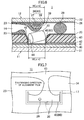
- FIGS. 5 and 6 show a second embodiment of the present invention.
- FIG. 5 is an enlarged plan view showing a region on a counter substrate 12 of a second embodiment facing a pad 20.
- FIG. 6 is an enlarged cross-sectional view showing a cross-sectional structure of a liquid crystal display device 1 of the second embodiment.
- the same components as those shown in FIGS. 1-4 will be indicated by the same reference characters to omit detailed description thereof.
- control structure 60 is formed in the TFT substrate 11. In the second embodiment, the control structure 60 is formed in both of the TFT substrate 11 and the counter substrate 12.
- the TFT substrate 11 has the same structure as that of the first embodiment.
- a width of the recessed groove 45 is about 50 ⁇ m so that a glass fiber 30 in the sealing member 14 can be contained in the recessed groove 45 as shown in FIG. 6 .
- the counter substrate 12 has a glass substrate 22 as a support substrate as shown in FIG. 6 .
- a plurality of color layers (not shown) constituting a color filter (not shown) and a black matrix (not shown) as a light shield film are formed on the surface of the glass substrate 22, and the common electrode 26 is formed on a surface of the color filter.
- the color layers are filters each transmitting red (R), green (G), or blue (B) light, and are arranged in a matrix pattern in the pixel region 31 on the counter substrate 12.
- the black matrix blocks light transmission through a region between the adjacent color layers, and blocks light transmission through the frame region 32.
- the sealing member 14 is the same as that formed on the TFT substrate 11, and is arranged in the sealing member region 34 in the frame region 32.
- An alignment film 23 extending from the pixel region 31 to the sealing member region 34 is formed on a surface of the counter substrate 12 facing the liquid crystal layer 13 by curing the same alignment film material 24 as that provided on the TFT substrate 11.
- a ridge portion 36 as the control structure 60 is formed on the surface of the glass substrate 22 to protrude toward the TFT substrate 11 and extend in the form of a rib. As shown in FIGS. 2 , 5 , and 6 , the ridge portion 36 is located inside the recessed groove 45 when viewed in a direction normal to the surface of the TFT substrate 11 or the counter substrate 12. Specifically, the ridge portion 36 is in the form of a rectangular ring covering part of the common electrode 26 as shown in FIG. 5 . Thus, part of the common electrode 26 surrounded by the rectangular ring-shaped ridge portion 36 is exposed from the alignment film 23.
- the ridge portion 36 includes a base 37 made of the same material as the blue color layer, for example, and a coating 38 which covers the base 37.
- the coating 38 is made of a photosensitive acrylic resin, which is the same material as a rib (not shown) or a photospacer (not shown) formed on the counter substrate 12 to align the liquid crystal molecules in vertical orientation.
- the ridge portion 36 includes inclined parts 39 constituting outer wall surfaces of the ridge portion 36, and part of the inclined parts 39 is covered with the alignment film 23.
- the ridge portion 36 is substantially tapered in a direction from the counter substrate 12 to the TFT substrate 11 as viewed in cross section of FIG. 6 .
- An outer one (a left one in FIG. 6 ) of the inclined parts 39 of the ring-shaped ridge portion 36 is covered with the alignment film 23, while an inner one (a right one in FIG. 6 ) of the inclined parts 39 is exposed from the alignment film 23.
- the inner inclined part 39 supports an edge of the alignment film 23.
- the base 37 has a thickness of about 2.5 ⁇ m, and a width of about 30 ⁇ m.
- the coating 38 on the base 37 has a thickness of about 4 ⁇ m, and a width of about 30 ⁇ m.
- a sealing member 14 is formed on a surface of the common electrode 26 in the sealing member region 34 to cover the ridge portion 36.
- conductive particles 29 in the sealing member 14 are sandwiched between the common electrode 26 exposed from the alignment film 23 and the pad 20 on the TFT substrate 11, thereby electrically connecting the pad 20 and the common electrode 26.
- the TFT substrate 11 is fabricated in the same manner as the first embodiment.
- a color filter (not shown) is formed on a surface of a glass substrate 22 which is a transparent substrate.
- a base 37 is simultaneously formed on a surface of the glass substrate 22 in a sealing member region 34 with the same material as the color layers.
- a common electrode 26 is formed to cover the base 37 and the color filter, and a photosensitive acrylic resin, for example, is deposited on a surface of the common electrode 26. Then, a coating 38 covering the base 37, and a photospacer (not shown) or a rib for aligning the liquid crystal molecules in vertical orientation are simultaneously formed by photolithography.
- an alignment film material 24 having fluidity such as polyimide, is supplied by ink jet printing to cover the color filter etc.
- the alignment film material 24 flows from the pixel region 31 to the frame region 32.
- an edge of the alignment film material 24 is supported by the inner inclined part 39 of the ridge portion 36.
- the alignment film material 24 bulges toward the TFT substrate 11 on the ridge portion 36 as shown in FIG. 6 , thereby stopping the flow of the alignment film material.
- the alignment film material 24 is then baked to form an alignment film 23.
- the counter substrate 12 is fabricated.
- the recessed groove 45 as the control structure 60 is formed in the TFT substrate 11 to expose the pad 20 from the alignment film 23.
- the ridge portion 36 as the control structure 60 is formed on the counter substrate 12 to expose part of the common electrode 26 facing the pad 20.
- the common electrode 26 and the conductive particle 29 are surly brought into contact, thereby electrically connecting the counter substrate 12 and the TFT substrate 11 with reliability.
- control structure 60 is made of the ring-shaped ridge portion 36 surrounding the part of the common electrode 26, the part of the common electrode 26 can surely be exposed from the alignment film 23.
- the ridge portion 36 is located inside the recessed groove 45 in the TFT substrate 11 when viewed in a direction normal to the surface of the substrate.
- the flow of the alignment film material 24 on the TFT substrate 11 toward the inside of the recessed groove 45 can surely be prevented.
- the sealing member 14 contains the glass fibers 30, the glass fiber 30 can be contained in the recessed groove 45 as shown in FIG. 6 . This can reduce the possibility that cell thickness (thickness of the liquid crystal layer 13) becomes uneven due to the glass fiber 30 sandwiched between the TFT substrate 11 and the counter substrate 12.
- the recessed groove 45 and the ridge portion 36 as the control structure 60 are in the form of a continuous ring.
- the present invention is not limited to the form, and the control structure 60 (the recessed groove 45 and the ridge portion 36) may be in the form of U when viewed in a direction normal to the surface of the TFT substrate 11 or the counter substrate 12, with their arms extending in a direction opposite the pixel region 31 (i.e., upward in FIG. 7 ) as shown in FIG. 7 corresponding to FIG. 2 .
- control structure 60 (the recessed groove 45 and the ridge portion 36) may be in the form of a ring which is chipped at part thereof opposite the pixel region 31 when viewed in a direction normal to the surface of the TFT substrate 11 or the counter substrate 12. This configuration can also provide the advantages similar to those of the first embodiment.
- the recessed groove 45 or the ridge portion 36 in the form of a single ring is formed as the control structure 60.
- the present invention is not limited thereto, and the recessed groove 45 or the ridge portion 36 may be formed in the form of double or triple rings coaxial with each other.
- the control structure 60 may be formed on at least one of the TFT substrate 11 or the counter substrate 12. However, for reliable electrical connection between the TFT substrate 11 and the counter substrate 12, the control structure 60 is preferably provided on each of the substrates 11, 12.
- the TFT substrate 11 and the counter substrate 12 are electrically conducted through the conductive particles 29 in the sealing member 14.
- the present invention is not limited thereto.
- the TFT substrate 11 and the counter substrate 12 may electrically be conducted through a different conductive material, such as conductive paste.
- the present invention is useful for the liquid crystal display devices.
Abstract
Description
- The present invention relates to liquid crystal display devices, particularly to control of application of an alignment film.
- In general, a liquid crystal display device includes a liquid crystal layer sealed between a pair of substrates. One of the paired substrates is a TFT substrate including a plurality of gate lines, a plurality of source lines, a plurality of pixel electrodes, a plurality of TFTs, etc. The other substrate is a counter substrate including a common electrode corresponding to the plurality of pixel electrodes. The liquid crystal layer is sealed with a frame-shaped sealing member surrounding the liquid crystal layer between the TFT substrate and the counter substrate.
- Each of the TFT substrate and the counter substrate includes an alignment film formed on a surface facing the liquid crystal layer to control orientation of liquid crystal molecules in the liquid crystal layer. The alignment film is made of a resin film, such as a polyimide film, and rubbing or photo-alignment has been performed on a surface thereof.
- The alignment film is formed by applying liquid polyimide on the surfaces of the TFT substrate and the counter substrate, and baking the liquid polyimide to cure. The polyimide may be applied by flexography, ink jet printing, etc.
- In forming the alignment film by the ink jet printing, viscosity of an alignment film material such as polyimide needs to be relatively low so that drops of the alignment film material discharged toward the substrate and hit on the substrate can sufficiently spread on the surface of the substrate. However, the low viscosity alignment film material can smoothly spread on the surface of the substrate, and the alignment film material may unnecessarily spread to a region for forming the sealing member.
-
Patent Documents 1 and 2 propose a technique of preventing the excessive spread of the alignment film material by forming a groove in the TFT substrate between the region for forming the sealing member and a pixel region which contributes to display so that the groove can hold the alignment film material. -
- [Patent Document 1] Japanese Patent Publication No.
2004-361623 - [Patent Document 2] Japanese Patent Publication No.
2007-322627 - When the groove is formed to hold the alignment film material therein as described in
Patent Documents 1 and 2, the groove needs to be relatively wide to ensure a capacity for holding the alignment film material. As a result, a distance between the pixel region and the sealing member region increases, and a frame-shaped non-display region formed around the pixel region cannot easily be narrowed. - According to another known technology, a plurality of electrode portions are formed in the sealing member region, and the electrode portions are conducted to the common electrode on the counter substrate through conductive particles dispersed and mixed in the sealing member.
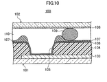
- Referring to an enlarged plan view of
FIG. 9 and an enlarged cross-sectional view ofFIG. 10 , the structure of the sealing member region of the liquid crystal display device according to a related technology will be described below in connection with a technical problem to be solved by the present invention. - A liquid
crystal display device 100 includes aTFT substrate 101 and acounter substrate 102 facing each other as shown inFIG. 10 . Afirst electrode 103 and aninterlayer insulating film 104 covering the first electrode are formed in a sealing member region for forming a sealing member on theTFT substrate 101. Anopening 105 is formed in theinterlayer insulating film 104 to penetrate theinterlayer insulating film 104 to reach part thefirst electrode 103. The opening 105 is rectangular when viewed in a direction normal to the substrate as shown inFIG. 9 . - A
second electrode 106 is formed on theTFT substrate 101 to directly cover a surface of the interlayerinsulating film 104, an inner wall surface of theopening 105, and thefirst electrode 103 exposed in theopening 105. Thus, thesecond electrode 106 is electrically connected to thefirst electrode 103. Thesecond electrode 106 may be made of a transparent conductive film, such as an indium tin oxide (ITO) film. Unlike the TFT substrates ofPatent Documents 1 and 2, theTFT substrate 101 is not provided with the groove. - An
alignment film 107 is formed on the interlayerinsulating film 104 to cover thesecond electrode 106. Thealignment film 107 is formed by spreading a low viscosity alignment film material from a pixel region (not shown) in an upward direction inFIG. 9 to cover thesecond electrode 106 and surround theopening 105. - A
common electrode 108 made of ITO etc. is formed on a surface of thecounter substrate 102 facing theTFT substrate 101. Part of thecommon electrode 108 faces thesecond electrode 106. Asealing member 110 in which a plurality ofconductive particles 109 are dispersed is provided between thecounter substrate 102 and theTFT substrate 101. Theconductive particles 109 are conducted with thecommon electrode 108. - However, since the
alignment film 107, which is an insulating film, extends to the sealing member region to cover thesecond electrode 106, thealignment film 107 which is present between thesecond electrode 106 and theconductive particles 109 may inhibit conduction between thesecond electrode 106 and thecommon electrode 108 through theconductive particles 109. - In view of the foregoing, the present invention has been achieved. The present invention is concerned with narrowing a non-display region of a liquid crystal display device as much as possible, while ensuring electrical connection between a pair of substrates.
- In view of the above concern, the present invention is directed to a liquid crystal display device including: a first substrate; a second substrate facing the first substrate; a liquid crystal layer provided between the first substrate and the second substrate; and a sealing member provided between the first substrate and the second substrate to surround and seal the liquid crystal layer.
- Each of the first substrate and the second substrate includes a pixel region as a display region, a frame region as a non-display region which surrounds the pixel region and includes a sealing member region for forming the sealing member, alignment films, each extending from the pixel region to the sealing member region, are formed on a surface of the first substrate facing the liquid crystal layer and a surface of the second substrate facing the liquid crystal layer, respectively, by curing an alignment film material having fluidity, electrode portions are formed in the sealing member regions of the first substrate and the second substrate, respectively, so that the electrode portions are electrically connected to each other through a conductive material, and a control structure is formed at least between the electrode portion and the pixel region on at least one of the first substrate and the second substrate to control a flow of the alignment film material before curing so that at least part of the electrode portion is exposed from the alignment film.
- Effects of the present invention will be described below.
- In fabricating the liquid crystal display device, the alignment film before curing spreads from the pixel region to the sealing member region. The flow of the alignment film material which reached the sealing member region is controlled by the control structure, and at least part of the electrode portion is not covered with the alignment film, and is kept exposed. Thus, the part of the electrode portion and the conductive material are electrically connected because the alignment film is not present therebetween.
- Even when a groove for holding the alignment film material is not formed between the pixel region and the sealing member region, the electrode portion on the first substrate and the electrode portion on the second substrate can electrically be connected through the conductive material. Thus, the frame region can greatly be narrowed, and the electrical connection between the first and second substrates can be ensured.
- According to the present invention, the electrode portion on the first substrate and the electrode portion on the second substrate can electrically be connected through the conductive material even when the groove for holding the alignment film material is not provided between the pixel region and the sealing member region. Thus, the frame region can greatly be narrowed, and the electrical connection between the first and second substrates can be ensured.
-
- [
FIG. 1] FIG. 1 is a plan view showing a schematic structure of a TFT substrate of a first embodiment. - [
FIG. 2] FIG. 2 is an enlarged plan view showing the vicinity of a pad on the TFT substrate of the first embodiment. - [
FIG. 3] FIG. 3 is a plan view showing an alignment film material flowing toward the pad on the TFT substrate of the first embodiment. - [
FIG. 4] FIG. 4 is an enlarged cross-sectional view showing a cross-sectional structure of a liquid crystal display device of the first embodiment. - [
FIG. 5] FIG. 5 is an enlarged plan view showing a region on a counter substrate of a second embodiment facing a pad. - [
FIG. 6] FIG. 6 is an enlarged cross-sectional view showing a cross-sectional structure of a liquid crystal display device of the second embodiment. - [
FIG. 7] FIG. 7 is a plan view corresponding toFIG. 2 , showing the vicinity of a pad on a TFT substrate of another embodiment. - [
FIG. 8] FIG. 8 is a plan view corresponding toFIG. 2 , showing the vicinity of a pad of a TFT substrate of still another embodiment. - [
FIG. 9] FIG. 9 is an enlarged plan view showing a sealing member region of a liquid crystal display device according to a related technology. - [
FIG. 10] FIG. 10 is an enlarged cross-sectional view showing the sealing member region of the liquid crystal display device according to the related technology. - Embodiments of the present invention will be described in detail below. The present invention is not limited to the following embodiments.
-
FIGS. 1-4 show a first embodiment of the present invention. -
FIG. 1 is a plan view showing a schematic structure of aTFT substrate 11 of the first embodiment.FIG. 2 is an enlarged plan view showing the vicinity of apad 20 on theTFT substrate 11 of the first embodiment.FIG. 3 is a plan view showing analignment film material 24 flowing toward thepad 20 on theTFT substrate 11 of the first embodiment.FIG. 4 is an enlarged cross-sectional view showing a cross-sectional structure of a liquidcrystal display device 1 of the first embodiment. - The liquid
crystal display device 1 includes, as shown inFIGS. 1 and4 , aTFT substrate 11 as a first substrate, acounter substrate 12 as a second substrate facing theTFT substrate 11, and aliquid crystal layer 13 provided between theTFT substrate 11 and thecounter substrate 12. - The liquid
crystal display device 1 further includes a sealingmember 14 provided between theTFT substrate 11 and thecounter substrate 12 to surround and seal theliquid crystal layer 13. The sealingmember 14 is substantially in the form of a rectangular frame as shown inFIG. 1 , and is made of a UV/thermally curable resin, such as an epoxy-based resin, in which a plurality ofconductive particles 29 as a conductive material andglass fibers 30 are dispersed and mixed. An outer diameter of theconductive particle 29 is about 5 µm, and a diameter of theglass fiber 30 is about 4 µm. A line width of the sealingmember 14 is about 0.5 mm, for example. - In
FIGS. 2 and 3 , only a singleconductive particle 29 is shown, and the other conductive agents are not shown for easy description. - Each of the
TFT substrate 11 and thecounter substrate 12 has apixel region 31 as a display region, and aframe region 32 as a non-display region surrounding thepixel region 31. Theframe region 32 includes a sealing member region 34 (a region for forming the sealing member 14) provided with a predetermined distance from thepixel region 31. -
Alignment films 23, each extending from thepixel region 31 to the sealingmember region 14, are formed on a surface of theTFT substrate 11 facing theliquid crystal layer 13 and a surface of thecounter substrate 12 facing theliquid crystal layer 13, respectively, by curing analignment film material 24 having fluidity. - The
alignment film 23 is made of a resin material such as polyimide, and controls initial orientation of liquid crystal molecules in theliquid crystal layer 13. Thealignment film material 24 has a viscosity reduced by adding a solvent to polyimide etc. Thealignment film material 24 may be, for example, a vertical alignment film material having a viscosity of 6.5 mPa·s manufactured by JSR Corporation. - The
counter substrate 12 has aglass substrate 22 as a support substrate as shown inFIG. 4 . Acommon electrode 26 as an electrode portion which is made of a transparent conductive film, such as an ITO film, and has a thickness of about 100 nm is formed on a surface of theglass substrate 22 facing theTFT substrate 11. Thecommon electrode 26 has a thickness of about 100 nm. - A plurality of pixels (not shown) are arranged in a matrix pattern in the
pixel region 31 of theTFT substrate 11. A pixel electrode (not shown) made of a transparent conductive film, such as an indium tin oxide (ITO) film, is formed in each of the pixels. A thin-film transistor (TFT, not shown) as a switching element connected to the pixel electrode is formed in each of the pixels. Gate lines (not shown) and source lines (not shown) connected to the TFTs are formed on theTFT substrate 11. - The
TFT substrate 11 has aglass substrate 21 as a support substrate as shown inFIG. 4 . A plurality of gate lines andlower electrodes 40 are formed on a surface of theglass substrate 21 facing thecounter substrate 12. Thelower electrodes 40 are arranged at predetermined intervals in the sealingmember region 34, and are made of the same material as the gate lines. Specifically, thelower electrode 40 is made of a 100 nm thick Ti film, a 300 nm thick Al film stacked on the Ti film, and a 50 nm thick Ti film stacked on the Al film. - As shown in
FIG. 1 , a plurality oflead lines 17 made of the same material as the gate lines are formed in theframe region 32 on theglass substrate 21. Some of the lead lines 17 are connected to thelower electrodes 40. A line width of thelead line 17 is about 10 µm. - A
gate insulating film 41 is formed on the surface of theglass substrate 21 to cover the gate lines and thelower electrodes 40 as shown inFIG. 4 . Thegate insulating film 41 is made of an oxide film, such as a SiO2 film, and has a thickness of about 0.4 µm. - A
passivation film 42 as a protective film is formed on a surface of thegate insulating film 41. Thepassivation film 42 is made of an inorganic film, such as a SiN film, and has a thickness of about 0.25 µm. - An interlayer insulating
film 43 is formed on a surface of thepassivation film 42 to cover thelower electrodes 40, etc. Theinterlayer insulating film 43 is made of a photosetting acrylic resin, for example, and has a thickness of about 2.5 µm. - A plurality of
pads 20 made of a transparent conductive film, such as an ITO film, are formed as an electrode portion on a surface of theinterlayer insulating film 43 in the sealingmember region 34 on theTFT substrate 11. Thepads 20 have a thickness of about 100 nm, and are arranged at predetermined intervals on the sealingmember 14 as shown inFIG. 1 . Thepads 20 are electrically connected to thecommon electrode 26 on thecounter substrate 12 through theconductive particles 29 in the sealingmember 14. Thepads 20 are arranged to face thelower electrodes 40, respectively. - An
opening 44 in the form of a slit is formed in theinterlayer insulating film 43, thepassivation film 42, and thegate insulating film 41 to expose thelower electrode 40. Thus, each of thepads 20 is formed on the surface of theinterlayer insulating film 43 and an inner surface of theopening 44. - Specifically, a recessed part of the
pad 20 forms a recessedgroove 45 in theopening 44. Thus, each of thepads 20 is electrically connected to thelower electrode 40 facing thepad 20 through theopening 44. - Thus, a
control structure 60 made of the recessedgroove 45 is formed in theTFT substrate 11 of the first embodiment. Thecontrol structure 60 is arranged at least between thepad 20 and thepixel region 31, and controls the flow of thealignment film material 24 before curing so that at least part of thepad 20 is exposed from thealignment film 23. Thecontrol structure 60 of the present embodiment is made of a rectangular ring-shaped recessedgroove 45 which covers at least part of thepad 20. Thus, part of thepad 20 surrounded by the rectangular ring-shaped recessedgroove 45 is exposed from thealignment film 23. - The recessed
groove 45 has aninclined part 46 constituting an inner wall surface of the recessedgroove 45, and part of theinclined part 46 is covered with thealignment film 23. Specifically, theinclined part 46 has a round convex surface forming a rim of the recessedgroove 45, and supports an edge of thealignment film 23. Thealignment film 23 is not formed inside the recessedgroove 45, and a bottom surface of the recessedgroove 45 is exposed from thealignment film 23. - As shown in
FIG. 3 , thepad 20 has a short side of about 500 µm, and a long side of about 3140 µm. A line width of the recessedgroove 45 is about 50 µm, and a distance between an outer edge of the recessedgroove 45 and an outer edge of thepad 20 is about 20 µm. Thus, part of thepad 20 having a short side of about 360 µm and a long side of about 3000 µm inside the recessedgroove 45 is exposed from thealignment film 23. - The sealing
member 14 is formed on the surface of theinterlayer insulating film 43 in the sealingmember region 34 to cover thepad 20 and the recessedgroove 45. Theconductive particles 29 in the sealingmember 14 are sandwiched between thepad 20 exposed from thealignment film 23 and thecommon electrode 26 of thecounter substrate 12, thereby electrically connecting thepad 20 and thecommon electrode 26. - A method for fabricating the liquid
crystal display device 1 will be described below. - The liquid
crystal display device 1 is fabricated by forming the frame-shaped sealingmember 14 on theTFT substrate 11 or thecounter substrate 12, dropping liquid crystal inside the sealingmember 14, and bonding theTFT substrate 11 and thecounter substrate 12. - In fabricating the
TFT substrate 11,lower electrodes 40 are formed simultaneously with gate lines (not shown) on a surface of aglass substrate 21 which is a transparent substrate. Then, agate insulating film 41, a silicon film (i layer, n+ phase, not shown), source lines (not shown), and apassivation film 42 are formed to cover the lower electrodes and the gate lines. Then, aninterlayer insulating film 43 is formed to cover the TFTs etc. - The
interlayer insulating film 43 can be made of a photosensitive organic material such as a photosetting acrylic region, or a non-photosensitive insulating film. When the photosensitive organic material is used, the organic material is applied to theglass substrate 21 to form a flat surface by spin coating (slit coating, or ink jet printing may be available). - Then, a slit-shaped
opening 44 penetrating theinterlayer insulating film 43, thepassivation film 42, and thegate insulating film 41 is formed by photolithography and etching. Thelower electrode 40 is exposed inside theopening 44. - When the non-photosensitive insulating film is used to form the
interlayer insulating film 43, an insulating material layer of a uniform thickness is formed on theglass substrate 21 by, for example, CVD (sputtering, or applying an applicable material may be available), and a photosensitive resist is applied to the entire surface of the insulating material layer. Then, a predetermined resist pattern is formed by photolithography. Then, the insulating material layer is etched (by wet or dry etching), and the resist pattern is removed, thereby forming theopening 44. - Then, an ITO layer is formed on a surface of the
interlayer insulating film 43, and is patterned by photolithography and etching to simultaneously form a plurality ofpads 20 and pixel electrodes (not shown). Thus, a recessedgroove 45 as acontrol structure 60 is formed inside theopening 44 by a recessed part of thepad 20. - Then, an
alignment film material 24 having fluidity, such as polyimide, is supplied by ink jet printing to cover the plurality ofpads 20 and the pixel electrodes. Thealignment film material 24 flows from thepixel region 31 to theframe region 32 as shown inFIG. 3 . When thealignment film material 24 reaches aninclined part 46 of the recessedgroove 45, an edge of thealignment film material 24 is supported by theinclined part 46. - As a result, the
alignment film material 24 bulges toward thecounter substrate 12 near theinclined part 46 of the recessedgroove 45 as shown inFIG. 4 , thereby stopping the flow of the alignment film material. Thus, the flow of thealignment film material 24 is controlled by the recessedgroove 45, and bypasses a region surrounded by the recessedgroove 45. Then, thealignment film material 24 is baked to form analignment film 23. Thus, theTFT substrate 11 is fabricated. - According to the first embodiment, the recessed
groove 45 as thecontrol structure 60 is formed between thepad 20 and thepixel region 31. Thus, the flow of thealignment film material 24 from thepixel region 31 to the sealingmember region 34 can be controlled by the recessedgroove 45, and part of thepads 20 is not covered, and can be exposed from thealignment film 23. Thus, the part of thepad 20 can directly be connected to theconductive particles 29 in the sealingmember 14 without thealignment film 23 interposed therebetween. - Thus, according to the first embodiment, the
pad 20 on theTFT substrate 11 and thecommon electrode 26 on thecounter substrate 12 can electrically be connected through theconductive particles 29 even when the groove for holding thealignment film material 24 is not formed between thepixel region 31 and the sealingmember region 34. Thus, theframe region 32 can greatly be narrowed, and the electrical connection between theTFT substrate 11 and thecounter substrate 12 can be ensured. - Since the recessed
groove 45 surrounding at least part of thepad 20 is formed as thecontrol structure 60, the surrounded part of thepad 20 can surely be exposed from thealignment film 23. - In addition, since the
control structure 60 also serves as a connector between thepad 20 and thelower electrode 40, there is no need to increase the non-display region only for the purpose of providing thecontrol structure 60. This can further narrow theframe region 32. -
FIGS. 5 and6 show a second embodiment of the present invention. -
FIG. 5 is an enlarged plan view showing a region on acounter substrate 12 of a second embodiment facing apad 20.FIG. 6 is an enlarged cross-sectional view showing a cross-sectional structure of a liquidcrystal display device 1 of the second embodiment. In the following embodiments, the same components as those shown inFIGS. 1-4 will be indicated by the same reference characters to omit detailed description thereof. - In the first embodiment, the
control structure 60 is formed in theTFT substrate 11. In the second embodiment, thecontrol structure 60 is formed in both of theTFT substrate 11 and thecounter substrate 12. - The
TFT substrate 11 has the same structure as that of the first embodiment. A width of the recessedgroove 45 is about 50 µm so that aglass fiber 30 in the sealingmember 14 can be contained in the recessedgroove 45 as shown inFIG. 6 . - The
counter substrate 12 has aglass substrate 22 as a support substrate as shown inFIG. 6 . Acommon electrode 26 made of a transparent conductive film, such as an ITO film, having a thickness of about 100 nm is formed on a surface of theglass substrate 22 facing theTFT substrate 11. A plurality of color layers (not shown) constituting a color filter (not shown) and a black matrix (not shown) as a light shield film are formed on the surface of theglass substrate 22, and thecommon electrode 26 is formed on a surface of the color filter. - The color layers are filters each transmitting red (R), green (G), or blue (B) light, and are arranged in a matrix pattern in the
pixel region 31 on thecounter substrate 12. The black matrix blocks light transmission through a region between the adjacent color layers, and blocks light transmission through theframe region 32. The sealingmember 14 is the same as that formed on theTFT substrate 11, and is arranged in the sealingmember region 34 in theframe region 32. - An
alignment film 23 extending from thepixel region 31 to the sealingmember region 34 is formed on a surface of thecounter substrate 12 facing theliquid crystal layer 13 by curing the samealignment film material 24 as that provided on theTFT substrate 11. - A
ridge portion 36 as thecontrol structure 60 is formed on the surface of theglass substrate 22 to protrude toward theTFT substrate 11 and extend in the form of a rib. As shown inFIGS. 2 ,5 , and6 , theridge portion 36 is located inside the recessedgroove 45 when viewed in a direction normal to the surface of theTFT substrate 11 or thecounter substrate 12. Specifically, theridge portion 36 is in the form of a rectangular ring covering part of thecommon electrode 26 as shown inFIG. 5 . Thus, part of thecommon electrode 26 surrounded by the rectangular ring-shapedridge portion 36 is exposed from thealignment film 23. - The
ridge portion 36 includes a base 37 made of the same material as the blue color layer, for example, and acoating 38 which covers thebase 37. Thecoating 38 is made of a photosensitive acrylic resin, which is the same material as a rib (not shown) or a photospacer (not shown) formed on thecounter substrate 12 to align the liquid crystal molecules in vertical orientation. - The
ridge portion 36 includesinclined parts 39 constituting outer wall surfaces of theridge portion 36, and part of theinclined parts 39 is covered with thealignment film 23. Theridge portion 36 is substantially tapered in a direction from thecounter substrate 12 to theTFT substrate 11 as viewed in cross section ofFIG. 6 . An outer one (a left one inFIG. 6 ) of theinclined parts 39 of the ring-shapedridge portion 36 is covered with thealignment film 23, while an inner one (a right one inFIG. 6 ) of theinclined parts 39 is exposed from thealignment film 23. Specifically, the innerinclined part 39 supports an edge of thealignment film 23. - As shown in
FIG. 6 , thebase 37 has a thickness of about 2.5 µm, and a width of about 30 µm. Thecoating 38 on thebase 37 has a thickness of about 4 µm, and a width of about 30 µm. - A sealing
member 14 is formed on a surface of thecommon electrode 26 in the sealingmember region 34 to cover theridge portion 36. Thus,conductive particles 29 in the sealingmember 14 are sandwiched between thecommon electrode 26 exposed from thealignment film 23 and thepad 20 on theTFT substrate 11, thereby electrically connecting thepad 20 and thecommon electrode 26. - A method for fabricating the liquid
crystal display device 1 will be described below. - The
TFT substrate 11 is fabricated in the same manner as the first embodiment. In fabricating thecounter substrate 12, a color filter (not shown) is formed on a surface of aglass substrate 22 which is a transparent substrate. In forming color layers (not shown) of the color filter, abase 37 is simultaneously formed on a surface of theglass substrate 22 in a sealingmember region 34 with the same material as the color layers. - Then, a
common electrode 26 is formed to cover thebase 37 and the color filter, and a photosensitive acrylic resin, for example, is deposited on a surface of thecommon electrode 26. Then, acoating 38 covering thebase 37, and a photospacer (not shown) or a rib for aligning the liquid crystal molecules in vertical orientation are simultaneously formed by photolithography. - Then, an
alignment film material 24 having fluidity, such as polyimide, is supplied by ink jet printing to cover the color filter etc. - The
alignment film material 24 flows from thepixel region 31 to theframe region 32. When thealignment film material 24 reaches theridge portion 36, an edge of thealignment film material 24 is supported by the innerinclined part 39 of theridge portion 36. As a result, thealignment film material 24 bulges toward theTFT substrate 11 on theridge portion 36 as shown inFIG. 6 , thereby stopping the flow of the alignment film material. Thealignment film material 24 is then baked to form analignment film 23. Thus, thecounter substrate 12 is fabricated. - According to the second embodiment, the recessed
groove 45 as thecontrol structure 60 is formed in theTFT substrate 11 to expose thepad 20 from thealignment film 23. Thus, the same advantages as those of the first embodiment can be obtained. In addition, theridge portion 36 as thecontrol structure 60 is formed on thecounter substrate 12 to expose part of thecommon electrode 26 facing thepad 20. Thus, thecommon electrode 26 and theconductive particle 29 are surly brought into contact, thereby electrically connecting thecounter substrate 12 and theTFT substrate 11 with reliability. - Since the
control structure 60 is made of the ring-shapedridge portion 36 surrounding the part of thecommon electrode 26, the part of thecommon electrode 26 can surely be exposed from thealignment film 23. - The
ridge portion 36 is located inside the recessedgroove 45 in theTFT substrate 11 when viewed in a direction normal to the surface of the substrate. Thus, the flow of thealignment film material 24 on theTFT substrate 11 toward the inside of the recessedgroove 45 can surely be prevented. Further, even when the sealingmember 14 contains theglass fibers 30, theglass fiber 30 can be contained in the recessedgroove 45 as shown inFIG. 6 . This can reduce the possibility that cell thickness (thickness of the liquid crystal layer 13) becomes uneven due to theglass fiber 30 sandwiched between theTFT substrate 11 and thecounter substrate 12. - In the first and second embodiments, the recessed
groove 45 and theridge portion 36 as thecontrol structure 60 are in the form of a continuous ring. However, the present invention is not limited to the form, and the control structure 60 (the recessedgroove 45 and the ridge portion 36) may be in the form of U when viewed in a direction normal to the surface of theTFT substrate 11 or thecounter substrate 12, with their arms extending in a direction opposite the pixel region 31 (i.e., upward inFIG. 7 ) as shown inFIG. 7 corresponding toFIG. 2 . - As shown in
FIG. 8 corresponding toFIG. 2 , the control structure 60 (the recessedgroove 45 and the ridge portion 36) may be in the form of a ring which is chipped at part thereof opposite thepixel region 31 when viewed in a direction normal to the surface of theTFT substrate 11 or thecounter substrate 12. This configuration can also provide the advantages similar to those of the first embodiment. - In the embodiments described above, the recessed
groove 45 or theridge portion 36 in the form of a single ring is formed as thecontrol structure 60. However, the present invention is not limited thereto, and the recessedgroove 45 or theridge portion 36 may be formed in the form of double or triple rings coaxial with each other. - The
control structure 60 may be formed on at least one of theTFT substrate 11 or thecounter substrate 12. However, for reliable electrical connection between theTFT substrate 11 and thecounter substrate 12, thecontrol structure 60 is preferably provided on each of thesubstrates - In the first and second embodiments, the
TFT substrate 11 and thecounter substrate 12 are electrically conducted through theconductive particles 29 in the sealingmember 14. However, the present invention is not limited thereto. For example, theTFT substrate 11 and thecounter substrate 12 may electrically be conducted through a different conductive material, such as conductive paste. - As described above, the present invention is useful for the liquid crystal display devices.
-
- 1
- Liquid crystal display device
- 11
- TFT substrate (first substrate)
- 12
- Counter substrate (second substrate)
- 13
- Liquid crystal layer
- 14
- Sealing member
- 20
- Pad (electrode portion)
- 23
- Alignment film
- 24
- Alignment film material
- 26
- Common electrode (electrode portion)
- 29
- Conductive particle (conductive material)
- 31
- Pixel region
- 32
- Frame region
- 34
- Sealing member region
- 36
- Ridge portion (control structure)
- 37
- Base
- 38
- Coating
- 39, 46
- Inclined part
- 40
- Lower electrode
- 43
- Interlayer insulating film
- 44
- Opening
- 45
- Recessed groove (control structure)
- 60
- Control structure
Claims (9)
- A liquid crystal display device comprising:a first substrate;a second substrate facing the first substrate;a liquid crystal layer provided between the first substrate and the second substrate; anda sealing member provided between the first substrate and the second substrate to surround and seal the liquid crystal layer, whereineach of the first substrate and the second substrate includes a pixel region as a display region, and a frame region as a non-display region which surrounds the pixel region and includes a sealing member region for forming the sealing member,alignment films, each extending from the pixel region to the sealing member region, are formed on a surface of the first substrate facing the liquid crystal layer and a surface of the second substrate facing the liquid crystal layer, respectively, by curing an alignment film material having fluidity,electrode portions are formed in the sealing member regions of the first substrate and the second substrate, respectively, so that the electrode portions are electrically connected to each other through a conductive material, anda control structure is formed at least between the electrode portion and the pixel region on at least one of the first substrate or the second substrate to control a flow of the alignment film material before curing so that at least part of the electrode portion is exposed from the alignment film.
- The liquid crystal display device of claim 1, wherein
the control structure is in the form of a ring surrounding the at least part of the electrode portion. - The liquid crystal display device of claim 1, wherein
the control structure is in the form of U when viewed in a direction normal to a surface of the first substrate or the second substrate, and arms of the control structure extend in a direction opposite the pixel region. - The liquid crystal display device of claim 1, wherein
the control structure is in the form of a ring which is chipped at part thereof opposite the pixel region when viewed in a direction normal to a surface of the first substrate or the second substrate. - The liquid crystal display device of any one of claims 1-4, wherein
the first substrate is provided with a lower electrode, an interlayer insulating film covering the lower electrode, and a slit-shaped opening penetrating the interlayer insulating film to expose the lower electrode,
the electrode portion of the first substrate is formed on a surface of the interlayer insulating film, and is connected to the lower electrode through the opening, and
a recessed groove formed inside the opening in the first substrate constitutes the control structure. - The liquid crystal display device of claim 5, wherein
the recessed groove includes an inclined part constituting an inner wall surface of the recessed groove, and
part of the inclined part of the recessed groove is covered with the alignment film. - The liquid crystal display device of any one of claims 1-6, wherein
a ridge portion formed on the second substrate to protrude toward the first substrate constitutes the control structure. - The liquid crystal display device of claim 5, wherein
a ridge portion formed on the second substrate to protrude toward the first substrate constitutes the control structure, and
the ridge portion is located in the recessed groove when viewed in a direction normal to a surface of the first substrate or the second substrate. - The liquid crystal display device of claim 7 or 8, wherein
the ridge portion includes an inclined part constituting an outer wall surface of the ridge portion, and
at least part of the inclined part of the ridge portion is covered with the alignment film.
Applications Claiming Priority (2)
| Application Number | Priority Date | Filing Date | Title |
|---|---|---|---|
| JP2010005819 | 2010-01-14 | ||
| PCT/JP2010/006608 WO2011086623A1 (en) | 2010-01-14 | 2010-11-10 | Liquid crystal display device |
Publications (2)
| Publication Number | Publication Date |
|---|---|
| EP2525251A1 true EP2525251A1 (en) | 2012-11-21 |
| EP2525251A4 EP2525251A4 (en) | 2013-10-30 |
Family
ID=44303929
Family Applications (1)
| Application Number | Title | Priority Date | Filing Date |
|---|---|---|---|
| EP20100842983 Withdrawn EP2525251A4 (en) | 2010-01-14 | 2010-11-10 | Liquid crystal display device |
Country Status (7)
| Country | Link |
|---|---|
| US (1) | US8922744B2 (en) |
| EP (1) | EP2525251A4 (en) |
| JP (1) | JP5379245B2 (en) |
| CN (1) | CN102656510B (en) |
| BR (1) | BR112012014142A2 (en) |
| RU (1) | RU2504811C1 (en) |
| WO (1) | WO2011086623A1 (en) |
Cited By (1)
| Publication number | Priority date | Publication date | Assignee | Title |
|---|---|---|---|---|
| EP2581784A1 (en) * | 2010-06-10 | 2013-04-17 | Sharp Kabushiki Kaisha | Liquid crystal display device and production method thereof |
Families Citing this family (5)
| Publication number | Priority date | Publication date | Assignee | Title |
|---|---|---|---|---|
| KR20110101906A (en) * | 2010-03-10 | 2011-09-16 | 삼성모바일디스플레이주식회사 | Liquid crystal display |
| KR101984269B1 (en) * | 2013-04-29 | 2019-05-30 | 엘지디스플레이 주식회사 | Liquid crystal display device and manufacturing method thereof |
| KR20160123424A (en) * | 2015-04-15 | 2016-10-26 | 삼성디스플레이 주식회사 | Liquid crystal display |
| CN105093693A (en) * | 2015-08-07 | 2015-11-25 | 京东方科技集团股份有限公司 | Display mother board, manufacturing method thereof, display panel and display device |
| CN105446019B (en) * | 2016-01-21 | 2019-08-02 | 深圳市华星光电技术有限公司 | A kind of display panel production method and liquid crystal display |
Citations (2)
| Publication number | Priority date | Publication date | Assignee | Title |
|---|---|---|---|---|
| US20080062360A1 (en) * | 2006-09-08 | 2008-03-13 | Setsuo Kobayashi | Liquid crystal display device |
| US20080123035A1 (en) * | 2006-11-27 | 2008-05-29 | Innolux Display Corp. | Liquid crystal display substrate with patterned area at periphery region thereof |
Family Cites Families (11)
| Publication number | Priority date | Publication date | Assignee | Title |
|---|---|---|---|---|
| JP2001100217A (en) * | 1999-09-29 | 2001-04-13 | Nec Corp | Color liquid crystal display device and method for manufacturing the same |
| JP4393662B2 (en) * | 2000-03-17 | 2010-01-06 | 株式会社半導体エネルギー研究所 | Method for manufacturing liquid crystal display device |
| JP3702858B2 (en) * | 2001-04-16 | 2005-10-05 | セイコーエプソン株式会社 | Electro-optical device and electronic apparatus |
| JP4156445B2 (en) | 2003-06-04 | 2008-09-24 | 株式会社 日立ディスプレイズ | Manufacturing method of liquid crystal display device |
| TWI306530B (en) * | 2003-10-01 | 2009-02-21 | Himax Tech Inc | Liquid crystal display panel and liquid crystal on silicon display panel |
| US20060136556A1 (en) * | 2004-12-17 | 2006-06-22 | Eclips, Llc | Systems and methods for personalizing audio data |
| JP4741870B2 (en) | 2005-04-18 | 2011-08-10 | Nec液晶テクノロジー株式会社 | Liquid crystal display device and manufacturing method thereof |
| CN101467097B (en) * | 2006-04-11 | 2012-01-11 | 夏普株式会社 | Board for display device and display device |
| JP4651580B2 (en) | 2006-05-31 | 2011-03-16 | 株式会社 日立ディスプレイズ | Liquid crystal display device |
| JP4820226B2 (en) | 2006-07-18 | 2011-11-24 | パナソニック液晶ディスプレイ株式会社 | Liquid crystal display |
| JP2009139779A (en) * | 2007-12-10 | 2009-06-25 | Hitachi Displays Ltd | Liquid crystal display device |
-
2010
- 2010-11-10 RU RU2012124087/28A patent/RU2504811C1/en not_active IP Right Cessation
- 2010-11-10 JP JP2011549756A patent/JP5379245B2/en active Active
- 2010-11-10 WO PCT/JP2010/006608 patent/WO2011086623A1/en active Application Filing
- 2010-11-10 EP EP20100842983 patent/EP2525251A4/en not_active Withdrawn
- 2010-11-10 US US13/515,075 patent/US8922744B2/en not_active Expired - Fee Related
- 2010-11-10 BR BR112012014142A patent/BR112012014142A2/en not_active IP Right Cessation
- 2010-11-10 CN CN201080056709.3A patent/CN102656510B/en active Active
Patent Citations (2)
| Publication number | Priority date | Publication date | Assignee | Title |
|---|---|---|---|---|
| US20080062360A1 (en) * | 2006-09-08 | 2008-03-13 | Setsuo Kobayashi | Liquid crystal display device |
| US20080123035A1 (en) * | 2006-11-27 | 2008-05-29 | Innolux Display Corp. | Liquid crystal display substrate with patterned area at periphery region thereof |
Non-Patent Citations (1)
| Title |
|---|
| See also references of WO2011086623A1 * |
Cited By (3)
| Publication number | Priority date | Publication date | Assignee | Title |
|---|---|---|---|---|
| EP2581784A1 (en) * | 2010-06-10 | 2013-04-17 | Sharp Kabushiki Kaisha | Liquid crystal display device and production method thereof |
| EP2581784A4 (en) * | 2010-06-10 | 2014-01-01 | Sharp Kk | Liquid crystal display device and production method thereof |
| US8885127B2 (en) | 2010-06-10 | 2014-11-11 | Sharp Kabushiki Kaisha | Liquid crystal display device and method for fabricating the same |
Also Published As
| Publication number | Publication date |
|---|---|
| EP2525251A4 (en) | 2013-10-30 |
| CN102656510A (en) | 2012-09-05 |
| RU2504811C1 (en) | 2014-01-20 |
| JP5379245B2 (en) | 2013-12-25 |
| US8922744B2 (en) | 2014-12-30 |
| US20120257152A1 (en) | 2012-10-11 |
| JPWO2011086623A1 (en) | 2013-05-16 |
| WO2011086623A1 (en) | 2011-07-21 |
| CN102656510B (en) | 2015-02-25 |
| BR112012014142A2 (en) | 2016-08-16 |
Similar Documents
| Publication | Publication Date | Title |
|---|---|---|
| US20220308375A1 (en) | Liquid crystal display device | |
| EP2525252A1 (en) | Liquid crystal display device and manufacturing method therefor | |
| US10529747B2 (en) | Display device | |
| US20230266626A1 (en) | Liquid crystal display device | |
| US8885127B2 (en) | Liquid crystal display device and method for fabricating the same | |
| US9417485B2 (en) | Liquid crystal display device | |
| JP6491825B2 (en) | Liquid crystal display | |
| US8922744B2 (en) | Liquid crystal display device | |
| US8749734B2 (en) | Liquid crystal display device with layers of different color filters covering light shielding films | |
| US20100182530A1 (en) | Display cell | |
| US20130010240A1 (en) | Display device and method for manufacturing the same | |
| KR20120052760A (en) | Electrophoretic display device and method of fabricating thereof | |
| JP2019082738A (en) | Liquid crystal display |
Legal Events
| Date | Code | Title | Description |
|---|---|---|---|
| PUAI | Public reference made under article 153(3) epc to a published international application that has entered the european phase |
Free format text: ORIGINAL CODE: 0009012 |
|
| 17P | Request for examination filed |
Effective date: 20120613 |
|
| AK | Designated contracting states |
Kind code of ref document: A1 Designated state(s): AL AT BE BG CH CY CZ DE DK EE ES FI FR GB GR HR HU IE IS IT LI LT LU LV MC MK MT NL NO PL PT RO RS SE SI SK SM TR |
|
| DAX | Request for extension of the european patent (deleted) | ||
| A4 | Supplementary search report drawn up and despatched |
Effective date: 20130927 |
|
| RIC1 | Information provided on ipc code assigned before grant |
Ipc: G02F 1/1339 20060101ALI20130923BHEP Ipc: G02F 1/1345 20060101ALI20130923BHEP Ipc: G02F 1/1333 20060101ALI20130923BHEP Ipc: G02F 1/1362 20060101ALI20130923BHEP Ipc: G02F 1/1337 20060101AFI20130923BHEP |
|
| 17Q | First examination report despatched |
Effective date: 20150513 |
|
| STAA | Information on the status of an ep patent application or granted ep patent |
Free format text: STATUS: EXAMINATION IS IN PROGRESS |
|
| STAA | Information on the status of an ep patent application or granted ep patent |
Free format text: STATUS: THE APPLICATION IS DEEMED TO BE WITHDRAWN |
|
| 18D | Application deemed to be withdrawn |
Effective date: 20170601 |