JP4651580B2 - Liquid crystal display device - Google Patents
Liquid crystal display device Download PDFInfo
- Publication number
- JP4651580B2 JP4651580B2 JP2006151478A JP2006151478A JP4651580B2 JP 4651580 B2 JP4651580 B2 JP 4651580B2 JP 2006151478 A JP2006151478 A JP 2006151478A JP 2006151478 A JP2006151478 A JP 2006151478A JP 4651580 B2 JP4651580 B2 JP 4651580B2
- Authority
- JP
- Japan
- Prior art keywords
- liquid crystal
- region
- crystal display
- display device
- groove
- Prior art date
- Legal status (The legal status is an assumption and is not a legal conclusion. Google has not performed a legal analysis and makes no representation as to the accuracy of the status listed.)
- Active
Links
- 239000004973 liquid crystal related substance Substances 0.000 title claims description 72
- 239000000758 substrate Substances 0.000 claims description 108
- 239000000463 material Substances 0.000 claims description 58
- 238000000034 method Methods 0.000 claims description 43
- 239000003566 sealing material Substances 0.000 claims description 28
- 238000007641 inkjet printing Methods 0.000 claims description 12
- AMGQUBHHOARCQH-UHFFFAOYSA-N indium;oxotin Chemical compound [In].[Sn]=O AMGQUBHHOARCQH-UHFFFAOYSA-N 0.000 claims description 3
- 230000001681 protective effect Effects 0.000 claims description 3
- 239000000565 sealant Substances 0.000 claims description 2
- 238000007789 sealing Methods 0.000 claims 1
- 239000011347 resin Substances 0.000 description 31
- 229920005989 resin Polymers 0.000 description 31
- 239000007788 liquid Substances 0.000 description 27
- 230000007480 spreading Effects 0.000 description 14
- 101100016388 Arabidopsis thaliana PAS2 gene Proteins 0.000 description 12
- 101100297150 Komagataella pastoris PEX3 gene Proteins 0.000 description 12
- 101100315760 Saccharomyces cerevisiae (strain ATCC 204508 / S288c) PEX4 gene Proteins 0.000 description 12
- 101100060179 Drosophila melanogaster Clk gene Proteins 0.000 description 11
- 101150038023 PEX1 gene Proteins 0.000 description 11
- 101150014555 pas-1 gene Proteins 0.000 description 11
- 238000009736 wetting Methods 0.000 description 10
- 230000004048 modification Effects 0.000 description 9
- 238000012986 modification Methods 0.000 description 9
- 239000004065 semiconductor Substances 0.000 description 7
- 230000005684 electric field Effects 0.000 description 6
- 239000011521 glass Substances 0.000 description 4
- 238000007639 printing Methods 0.000 description 4
- 239000013256 coordination polymer Substances 0.000 description 3
- 101100353517 Caenorhabditis elegans pas-2 gene Proteins 0.000 description 2
- 229910021417 amorphous silicon Inorganic materials 0.000 description 2
- 230000002093 peripheral effect Effects 0.000 description 2
- 230000009467 reduction Effects 0.000 description 2
- 101100245267 Caenorhabditis elegans pas-1 gene Proteins 0.000 description 1
- 239000004642 Polyimide Substances 0.000 description 1
- 239000003990 capacitor Substances 0.000 description 1
- 239000011248 coating agent Substances 0.000 description 1
- 238000000576 coating method Methods 0.000 description 1
- 239000012141 concentrate Substances 0.000 description 1
- 238000011109 contamination Methods 0.000 description 1
- 230000002950 deficient Effects 0.000 description 1
- 238000010586 diagram Methods 0.000 description 1
- 230000000694 effects Effects 0.000 description 1
- 239000007772 electrode material Substances 0.000 description 1
- 238000002347 injection Methods 0.000 description 1
- 239000007924 injection Substances 0.000 description 1
- 239000011159 matrix material Substances 0.000 description 1
- 229920001721 polyimide Polymers 0.000 description 1
- 230000008569 process Effects 0.000 description 1
- 239000007787 solid Substances 0.000 description 1
- 239000000243 solution Substances 0.000 description 1
Images


Classifications
-
- G—PHYSICS
- G02—OPTICS
- G02F—OPTICAL DEVICES OR ARRANGEMENTS FOR THE CONTROL OF LIGHT BY MODIFICATION OF THE OPTICAL PROPERTIES OF THE MEDIA OF THE ELEMENTS INVOLVED THEREIN; NON-LINEAR OPTICS; FREQUENCY-CHANGING OF LIGHT; OPTICAL LOGIC ELEMENTS; OPTICAL ANALOGUE/DIGITAL CONVERTERS
- G02F1/00—Devices or arrangements for the control of the intensity, colour, phase, polarisation or direction of light arriving from an independent light source, e.g. switching, gating or modulating; Non-linear optics
- G02F1/01—Devices or arrangements for the control of the intensity, colour, phase, polarisation or direction of light arriving from an independent light source, e.g. switching, gating or modulating; Non-linear optics for the control of the intensity, phase, polarisation or colour
- G02F1/13—Devices or arrangements for the control of the intensity, colour, phase, polarisation or direction of light arriving from an independent light source, e.g. switching, gating or modulating; Non-linear optics for the control of the intensity, phase, polarisation or colour based on liquid crystals, e.g. single liquid crystal display cells
- G02F1/133—Constructional arrangements; Operation of liquid crystal cells; Circuit arrangements
- G02F1/1333—Constructional arrangements; Manufacturing methods
- G02F1/1337—Surface-induced orientation of the liquid crystal molecules, e.g. by alignment layers
- G02F1/133711—Surface-induced orientation of the liquid crystal molecules, e.g. by alignment layers by organic films, e.g. polymeric films
-
- G—PHYSICS
- G02—OPTICS
- G02F—OPTICAL DEVICES OR ARRANGEMENTS FOR THE CONTROL OF LIGHT BY MODIFICATION OF THE OPTICAL PROPERTIES OF THE MEDIA OF THE ELEMENTS INVOLVED THEREIN; NON-LINEAR OPTICS; FREQUENCY-CHANGING OF LIGHT; OPTICAL LOGIC ELEMENTS; OPTICAL ANALOGUE/DIGITAL CONVERTERS
- G02F1/00—Devices or arrangements for the control of the intensity, colour, phase, polarisation or direction of light arriving from an independent light source, e.g. switching, gating or modulating; Non-linear optics
- G02F1/01—Devices or arrangements for the control of the intensity, colour, phase, polarisation or direction of light arriving from an independent light source, e.g. switching, gating or modulating; Non-linear optics for the control of the intensity, phase, polarisation or colour
- G02F1/13—Devices or arrangements for the control of the intensity, colour, phase, polarisation or direction of light arriving from an independent light source, e.g. switching, gating or modulating; Non-linear optics for the control of the intensity, phase, polarisation or colour based on liquid crystals, e.g. single liquid crystal display cells
- G02F1/133—Constructional arrangements; Operation of liquid crystal cells; Circuit arrangements
- G02F1/1333—Constructional arrangements; Manufacturing methods
- G02F1/1339—Gaskets; Spacers; Sealing of cells
-
- G—PHYSICS
- G02—OPTICS
- G02F—OPTICAL DEVICES OR ARRANGEMENTS FOR THE CONTROL OF LIGHT BY MODIFICATION OF THE OPTICAL PROPERTIES OF THE MEDIA OF THE ELEMENTS INVOLVED THEREIN; NON-LINEAR OPTICS; FREQUENCY-CHANGING OF LIGHT; OPTICAL LOGIC ELEMENTS; OPTICAL ANALOGUE/DIGITAL CONVERTERS
- G02F1/00—Devices or arrangements for the control of the intensity, colour, phase, polarisation or direction of light arriving from an independent light source, e.g. switching, gating or modulating; Non-linear optics
- G02F1/01—Devices or arrangements for the control of the intensity, colour, phase, polarisation or direction of light arriving from an independent light source, e.g. switching, gating or modulating; Non-linear optics for the control of the intensity, phase, polarisation or colour
- G02F1/13—Devices or arrangements for the control of the intensity, colour, phase, polarisation or direction of light arriving from an independent light source, e.g. switching, gating or modulating; Non-linear optics for the control of the intensity, phase, polarisation or colour based on liquid crystals, e.g. single liquid crystal display cells
- G02F1/133—Constructional arrangements; Operation of liquid crystal cells; Circuit arrangements
- G02F1/1333—Constructional arrangements; Manufacturing methods
- G02F1/133388—Constructional arrangements; Manufacturing methods with constructional differences between the display region and the peripheral region
Description
本発明は、液晶表示装置に関し、特に、配向膜の塗布領域の制御に適用して有効な技術に関するものである。 The present invention relates to a liquid crystal display device, and more particularly to a technique effective when applied to control of a coating region of an alignment film.
従来、映像や画像を表示する表示装置には、一対の基板の間に液晶材料を封入した液晶表示パネルを用いた液晶表示装置がある。 Conventionally, there is a liquid crystal display device using a liquid crystal display panel in which a liquid crystal material is sealed between a pair of substrates.
前記液晶表示パネルは、一対の基板のうちの一方の基板に、たとえば、複数本の走査信号線、複数本の映像信号線が形成されている。そして、2本の隣接する走査信号線と2本の隣接する映像信号線で囲まれた領域が1つの画素領域に相当し、各画素領域に対してTFT素子や画素電極などが配置されている。この基板は、一般に、TFT基板と呼ばれる。また、前記TFT基板と対をなす他方の基板は、一般に、対向基板と呼ばれる。 In the liquid crystal display panel, for example, a plurality of scanning signal lines and a plurality of video signal lines are formed on one of a pair of substrates. A region surrounded by two adjacent scanning signal lines and two adjacent video signal lines corresponds to one pixel region, and a TFT element, a pixel electrode, or the like is arranged in each pixel region. . This substrate is generally called a TFT substrate. The other substrate paired with the TFT substrate is generally called a counter substrate.
また、前記液晶表示パネルが、たとえば、TN方式やVA方式のような縦電界方式と呼ばれる駆動方式の場合、前記TFT基板の前記画素電極と対向する対向電極(共通電極とも呼ばれる)は、前記対向基板に設けられる。また、前記液晶表示パネルが、たとえば、IPS方式のような横電界方式と呼ばれる駆動方式の場合、前記対向電極は、前記TFT基板に設けられる。 In addition, when the liquid crystal display panel is a driving method called a vertical electric field method such as a TN method or a VA method, a counter electrode (also referred to as a common electrode) facing the pixel electrode of the TFT substrate is Provided on the substrate. Further, when the liquid crystal display panel is of a driving method called a lateral electric field method such as an IPS method, the counter electrode is provided on the TFT substrate.
また、前記TFT基板および前記対向基板は、前記画素電極と前記対向電極の電位差がない状態における液晶分子の向き(配向)や、前記画素電極と前記対向電極の間に電位差が生じたときの液晶分子の配列や傾きを制御するための配向膜が設けられている。 In addition, the TFT substrate and the counter substrate are liquid crystal when a potential difference is generated between the pixel electrode and the counter electrode, and the orientation (orientation) of liquid crystal molecules in a state where there is no potential difference between the pixel electrode and the counter electrode. An alignment film for controlling the arrangement and inclination of molecules is provided.
前記配向膜は、各基板の液晶材料(液晶層)との界面に設けられており、たとえば、前記画素領域の集合からなる表示領域全体を覆うように形成されたポリイミドなどの樹脂膜の表面にラビング処理を行って形成している。 The alignment film is provided at the interface with the liquid crystal material (liquid crystal layer) of each substrate. For example, the alignment film is formed on the surface of a resin film such as polyimide formed so as to cover the entire display area including the set of pixel areas. It is formed by rubbing treatment.
また、前記各基板の表面に形成する樹脂膜は、従来、たとえば、フレキソ印刷法と呼ばれる方法で形成していたが、近年は、インクジェット印刷法を用いて形成する方法が提案されている(たとえば、特許文献1を参照。)。前記インクジェット印刷法には、基板上に直接描画ができ、非接触プロセスによる低汚染、溶液消費量の低減、段取り時間の短縮などの種々の利点がある。
しかしながら、前記インクジェット印刷法で配向膜を形成する場合、その周辺における寸法制御および形状制御が困難であることが指摘されている。すなわち、インクジェット印刷法で樹脂膜の材料を基板上に印刷した場合、印刷領域の制御が難しいという問題があった。 However, it has been pointed out that when an alignment film is formed by the ink jet printing method, it is difficult to control the dimensions and shape in the periphery. That is, when the resin film material is printed on the substrate by the inkjet printing method, there is a problem that it is difficult to control the print area.
このような問題は、たとえば、インクジェット印刷法で用いる材料の粘度が、前記フレキソ印刷法などで用いられる材料の粘度に比べて低いことが原因とされている。 Such a problem is caused, for example, by the fact that the viscosity of the material used in the ink jet printing method is lower than the viscosity of the material used in the flexographic printing method or the like.
そのため、たとえば、走査信号線、映像信号線、TFT素子、画素電極などが形成されたTFT基板の表面に、インクジェット印刷法で配向膜を形成すると、たとえば、印刷した材料が濡れ広がり、シール材を形成する領域まで到達してしまうことがある。このように、配向膜がシール材を形成する領域まで到達してしまうと、たとえば、シール材とTFT基板(配向膜)との密着性が不十分で液晶材料が漏れたりするという問題がある。 Therefore, for example, when an alignment film is formed on the surface of a TFT substrate on which scanning signal lines, video signal lines, TFT elements, pixel electrodes, etc. are formed by an ink jet printing method, for example, the printed material is spread and the sealing material is used. The region to be formed may be reached. Thus, if the alignment film reaches the region where the sealing material is formed, for example, there is a problem that the liquid crystal material leaks due to insufficient adhesion between the sealing material and the TFT substrate (alignment film).
前記インクジェット印刷法で配向膜を形成するときに、印刷した材料がシール材を形成する領域まで濡れ広がらないようにする方法としては、たとえば、印刷した材料の濡れ広がりの量を考慮して、あらかじめ印刷する領域を小さくする方法が考えられる。しかしながら、この方法では、表示領域内で印刷した材料の膜厚にばらつきが生じ易いという問題がある。 When forming the alignment film by the inkjet printing method, as a method for preventing the printed material from getting wet to the area where the sealing material is formed, for example, considering the amount of wet spreading of the printed material in advance, A method for reducing the printing area is conceivable. However, this method has a problem that the film thickness of the material printed in the display area tends to vary.
また、その他にも、たとえば、印刷する材料の粘度を高くして濡れ広がりを抑制する方法が考えられる。しかしながら、この方法では、印刷時の射出不良により材料が塗布されない領域が発生しやすいという問題がある。 In addition, for example, a method of suppressing wetting and spreading by increasing the viscosity of the material to be printed is conceivable. However, this method has a problem that a region where no material is applied is likely to occur due to defective injection during printing.
本発明の目的は、たとえば、液晶表示パネルの配向膜の、表示領域の外側での濡れ広がりを抑制し、かつ、表示領域内における膜厚の均一性を維持することが可能な技術を提供することにある。 An object of the present invention is to provide, for example, a technique capable of suppressing the wetting and spreading of the alignment film of a liquid crystal display panel outside the display area and maintaining the uniformity of the film thickness in the display area. There is.
本発明の前記ならびにその他の目的と新規な特徴は、本明細書の記述および添付図面によって明らかになるであろう。 The above and other objects and novel features of the present invention will be apparent from the description of this specification and the accompanying drawings.
本願において開示される発明のうち、代表的なものの概略を説明すれば、以下の通りである。 The outline of typical inventions among the inventions disclosed in the present application will be described as follows.
(1)一対の基板の間に環状のシール材が配置され、前記一対の基板と前記シール材で囲まれた空間に液晶材料が封入されており、平面でみて前記一対の基板および液晶材料が重なる領域に表示領域が構成された表示パネルを有する液晶表示装置であって、前記一対の基板は、相対する基板と対向する面の表面に配向膜を有し、前記一対の基板のうちの少なくとも一方の基板は、前記シール材が配置される領域よりも内側であり、かつ、前記表示領域の外側である環状の領域において、前記配向膜と前記基板との間に、第1の導電層および第2の導電層と、前記第1の導電層と前記第2の導電層との間に介在する絶縁層とを有し、前記絶縁層は、少なくとも前記表示領域の外周に沿った方向に延設され、かつ、前記配向膜側が開口した凹溝を有し、前記第1の導電層は、前記凹溝の形状に沿って形成されている液晶表示装置。 (1) An annular sealing material is disposed between a pair of substrates, and a liquid crystal material is enclosed in a space surrounded by the pair of substrates and the sealing material. A liquid crystal display device having a display panel in which a display region is formed in an overlapping region, wherein the pair of substrates has an alignment film on a surface facing a facing substrate, and at least one of the pair of substrates One substrate has a first conductive layer and an intermediate region between the alignment film and the substrate in an annular region inside the region where the sealing material is disposed and outside the display region. A second conductive layer; and an insulating layer interposed between the first conductive layer and the second conductive layer, the insulating layer extending at least in a direction along an outer periphery of the display region. It is set, and a concave groove the alignment layer side is opened And, wherein the first conductive layer, a liquid crystal display device which is formed along the shape of the groove.
(2)前記(1)の液晶表示装置において、前記絶縁層を有する基板は、複数本の走査信号線と、前記複数本の走査信号線と立体的に交差する複数本の映像信号線と、前記表示領域内に配置された複数のTFT素子および複数の画素電極とを有し、前記第1の導電層は、前記画素電極と同じ材料でなる液晶表示装置。 (2) In the liquid crystal display device according to (1), the substrate having the insulating layer includes a plurality of scanning signal lines, a plurality of video signal lines sterically intersecting with the plurality of scanning signal lines, A liquid crystal display device having a plurality of TFT elements and a plurality of pixel electrodes arranged in the display region , wherein the first conductive layer is made of the same material as the pixel electrodes.
(3)前記(2)の液晶表示装置において、前記環状領域は、外周および内周が矩形状であり、前記走査信号線は、前記環状領域の一辺において、前記表示領域から前記シール材へ向かう方向で前記環状領域を横断しており、前記凹溝は、前記環状領域内の前記走査信号線の間毎に設けられている液晶表示装置。
(4)前記(3)の液晶表示装置において、前記走査信号線の間に設けられた前記凹溝は、前記表示領域の外周に沿って延設される溝と、前記表示領域から前記シール材へ向かう方向に沿って延設される溝とを有する液晶表示装置。
(5)前記(2)の液晶表示装置において、前記環状領域は、外周および内周が矩形状であり、前記映像信号線は、前記環状領域の一辺において、前記表示領域から前記シール材へ向かう方向で前記環状領域を横断しており、前記凹溝は、前記環状領域内の前記映像信号線の間毎に設けられている液晶表示装置。
(3) In the liquid crystal display device of (2), the annular region has a rectangular outer periphery and inner periphery, and the scanning signal line is directed from the display region to the sealing material on one side of the annular region. A liquid crystal display device that crosses the annular region in a direction and is provided between the scanning signal lines in the annular region .
(4) In the liquid crystal display device of (3), the concave groove provided between the scanning signal lines includes a groove extending along an outer periphery of the display area, and the sealing material from the display area. A liquid crystal display device having a groove extending along a direction toward the head.
(5) In the liquid crystal display device of (2), the annular region has a rectangular outer periphery and inner periphery, and the video signal line is directed from the display region to the sealing material on one side of the annular region. A liquid crystal display device that crosses the annular region in a direction, and the groove is provided between the video signal lines in the annular region.
(6)前記(2)の液晶表示装置において、前記第2の導電層は、保護ダイオードの一部を形成するものであり、前記保護ダイオードは、前記環状領域内に、前記表示領域に沿って形成されている液晶表示装置。 ( 6 ) In the liquid crystal display device of (2), the second conductive layer forms a part of a protective diode, and the protective diode is disposed in the annular region along the display region. Liquid crystal display device being formed .
(7)前記(2)の液晶表示装置において、前記絶縁層を有する基板は、前記表示領域内に配置された共通電極を有し、前記第2の導電層は、前記共通電極に電気信号を供給するコモンバスラインであり、前記コモンバスラインは、前記環状領域内に、前記表示領域に沿って形成されている液晶表示装置。
(8)前記(7)の液晶表示装置において、前記環状領域は、外周および内周が矩形状であり、前記走査信号線は、前記環状領域の一辺において、前記表示領域から前記シール材へ向かう方向で前記環状領域を横断しており、前記映像信号線は、前記環状領域の他の一辺において、前記表示領域から前記シール材へ向かう方向で前記環状領域を横断しており、前記環状領域の前記走査信号線および前記映像信号線が横断していない辺において、前記凹溝は、前記コモンバスライン上に、前記表示領域に沿って延設置されている液晶表示装置。
( 7 ) In the liquid crystal display device according to (2), the substrate having the insulating layer has a common electrode disposed in the display region, and the second conductive layer sends an electric signal to the common electrode. A common bus line to be supplied, wherein the common bus line is formed in the annular region along the display region .
(8) In the liquid crystal display device according to (7), the annular region has a rectangular outer periphery and inner periphery, and the scanning signal line is directed from the display region to the sealing material on one side of the annular region. The video signal line crosses the annular region in a direction from the display region to the sealing material on the other side of the annular region, and the video signal line crosses the annular region in a direction. In the side where the scanning signal line and the video signal line do not cross, the concave groove extends on the common bus line along the display area.
(9)前記(1)の液晶表示装置において、前記第1の導電層は、ITO(Indium Tin Oxide)である液晶表示装置。 ( 9 ) The liquid crystal display device according to ( 1 ), wherein the first conductive layer is ITO (Indium Tin Oxide) .
(10)前記(1)の液晶表示装置において、前記配向膜は、配向膜材料をインクジェット印刷法で塗布して形成されたものである液晶表示装置。 ( 10 ) The liquid crystal display device according to (1 ) , wherein the alignment film is formed by applying an alignment film material by an inkjet printing method .
本発明の液晶表示装置は、液晶表示パネルの一対の基板のうちの少なくとも一方の基板の、シール材が配置される領域よりも内側であり、かつ、表示領域の外側である概略環状の領域に、前記表示領域の外周に沿った方向に長く延びる溝部を有する。このとき、前記溝部は、前記絶縁層を開口して設けた凹溝と、前記凹溝の側面および底面に延在する導電層で構成されており、前記導電層は、前記透明電極と同じ材料でなることを特徴とする。このようにすると、前記溝部を有する基板の表示領域に液状の樹脂材料を印刷または塗布して配向膜を形成するときに、印刷した液状の樹脂材料が表示領域の外側に広がっても、前記溝部において前記樹脂材料の広がりが止まる。そのため、液晶表示パネルの配向膜の、表示領域の外側での濡れ広がりを抑制し、かつ、表示領域内における膜厚の均一性を維持することができる。 In the liquid crystal display device of the present invention, at least one of the pair of substrates of the liquid crystal display panel is located on the inner side of the region where the sealing material is disposed and in the substantially annular region outside the display region. And a groove extending long in the direction along the outer periphery of the display area. At this time, the groove portion is composed of a groove formed by opening the insulating layer, and a conductive layer extending on the side surface and the bottom surface of the groove, and the conductive layer is made of the same material as the transparent electrode. It is characterized by the following. In this case, when the liquid resin material is printed or applied to the display region of the substrate having the groove portion to form the alignment film, the groove portion is not affected even if the printed liquid resin material spreads outside the display region. The spread of the resin material stops. Therefore, it is possible to suppress the wetting and spreading of the alignment film of the liquid crystal display panel outside the display area and to maintain the uniformity of the film thickness within the display area.
また、前記溝部は、液晶表示パネルの一対の基板の両方に設けることが望ましいが、特に、前記溝部を有する基板は、複数本の走査信号線と、前記複数本の走査信号線と立体的に交差する複数本の映像信号線と、2本の隣接する走査信号線と2本の隣接する映像信号線で囲まれた領域に対して配置されるTFT素子および画素電極とを有する基板(TFT基板と呼ばれる)に設けることが望ましい。 The groove is preferably provided on both of the pair of substrates of the liquid crystal display panel. In particular, the substrate having the groove is three-dimensionally formed with a plurality of scanning signal lines and the plurality of scanning signal lines. Substrate (TFT substrate) having a plurality of intersecting video signal lines, TFT elements and pixel electrodes arranged in a region surrounded by two adjacent scanning signal lines and two adjacent video signal lines It is desirable to provide it.
また、前記TFT基板に前記溝部を設ける場合、前記複数本の走査信号線の、走査信号が入力される端部の近くに設ける前記溝部の前記凹溝は、たとえば、2本の隣接する走査信号線の間毎に設ける。またこのとき、前記凹溝が表示領域に近い位置にあると、たとえば、印刷した液状の樹脂材料の跳ね返りで表示領域の外周部における配向膜の膜厚にムラが生じる可能性がある。そのため、前記凹溝(溝部)は、表示領域から遠ざけることが望ましい。 Further, when the groove portion is provided on the TFT substrate, the concave groove of the groove portion provided near the end portion to which the scanning signal is input of the plurality of scanning signal lines is, for example, two adjacent scanning signals. Provided between each line. At this time, if the concave groove is located at a position close to the display area, the film thickness of the alignment film in the outer peripheral portion of the display area may be uneven due to, for example, rebounding of the printed liquid resin material. Therefore, it is desirable that the concave groove (groove portion) be kept away from the display area.
また、前記複数本の走査信号線の、走査信号が入力される端部と反対側の端部の近く設ける前記溝部の前記凹溝は、前記走査信号線の前記反対側の端部と前記シール材が配置される領域の間に設け、表示領域の外周に沿った長さを、2本の隣接する走査信号線の間隔よりも長くする。このとき、前記溝部は、表示領域の外周に沿った長さが、複数本の走査信号線のうち、最外側にある2本の走査信号線の間隔よりも長い1本の凹溝と前記導電層で構成することが望ましい。 Further, the groove of the groove provided near the end opposite to the end to which the scanning signal is input of the plurality of scanning signal lines is connected to the opposite end of the scanning signal line and the seal. It is provided between the regions where the material is arranged, and the length along the outer periphery of the display region is made longer than the interval between two adjacent scanning signal lines. At this time, the groove portion has a length along the outer periphery of the display region that is longer than a distance between two outermost scanning signal lines among the plurality of scanning signal lines, and the conductive portion. It is desirable to be composed of layers.
また、前記複数本の映像信号線の、映像信号が入力される端部の近くに設ける前記溝部の前記凹溝は、たとえば、2本の隣接する映像信号線の間毎に設ける。またこのときも、前記凹溝が表示領域に近い位置にあると、たとえば、印刷した液状の樹脂材料の跳ね返りで表示領域の外周部における配向膜の膜厚にムラが生じる可能性がある。そのため、前記凹溝(溝部)は、表示領域から遠ざけることが望ましい。 Further, the concave groove of the groove portion provided near the end portion to which the video signal is input of the plurality of video signal lines is provided, for example, between every two adjacent video signal lines. Also at this time, if the groove is close to the display area, for example, the printed liquid resin material may be rebounded to cause unevenness in the film thickness of the alignment film on the outer periphery of the display area. Therefore, it is desirable that the concave groove (groove portion) be kept away from the display area.
また、前記複数本の映像信号線の、映像信号が入力される端部と反対側の端部の近く設ける前記溝部の前記凹溝は、前記映像信号線の前記反対側の端部と前記シール材が配置される領域の間に設け、表示領域の外周に沿った長さを、2本の隣接する映像信号線の間隔よりも長くする。このとき、前記溝部は、表示領域の外周に沿った長さが、複数本の映像信号線のうち、最外側にある2本の映像信号線の間隔よりも長い1本の凹溝と前記導電層で構成することが望ましい。 In addition, the groove of the groove provided near the end opposite to the end where the video signal is input of the plurality of video signal lines is connected to the opposite end of the video signal line and the seal. It is provided between the areas where the material is arranged, and the length along the outer periphery of the display area is made longer than the interval between two adjacent video signal lines. At this time, the groove portion has a length along the outer periphery of the display region that is longer than the interval between two outermost video signal lines among the plurality of video signal lines, and the conductive portion. It is desirable to be composed of layers.
また、前記溝部の導電層を透明電極(画素電極)と同じ材料で設ける場合、その材料には、たとえば、ITO(Indium Tin Oxide)がある。 Further, when the conductive layer of the groove is formed of the same material as the transparent electrode (pixel electrode), the material is, for example, ITO (Indium Tin Oxide).
以下、本発明について、図面を参照して実施の形態(実施例)とともに詳細に説明する。
なお、実施例を説明するための全図において、同一機能を有するものは、同一符号を付け、その繰り返しの説明は省略する。
Hereinafter, the present invention will be described in detail together with embodiments (examples) with reference to the drawings.
In all the drawings for explaining the embodiments, parts having the same function are given the same reference numerals and their repeated explanation is omitted.
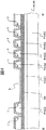
図1は、本発明による一実施例の液晶表示パネルの概略構成を示す模式平面図である。図2は、図1のA−A’線における模式断面図である。 FIG. 1 is a schematic plan view showing a schematic configuration of a liquid crystal display panel according to an embodiment of the present invention. FIG. 2 is a schematic cross-sectional view taken along the line A-A ′ of FIG. 1.
本発明の表示装置は、たとえば、図1および図2に示すように、一対の基板1,2の間に環状のシール材3が配置され、一対の基板1,2とシール材3で囲まれた空間に液晶材料4が封入された液晶表示パネルを有する液晶表示装置である。このとき、映像または画像を表示する表示領域DAは、平面でみて一対の基板1,2および液晶材料4が重なる領域に形成されている。
In the display device of the present invention, for example, as shown in FIGS. 1 and 2, an
また、一対の基板1,2は平面でみた外形寸法が異なり、液晶表示装置が、たとえば、テレビやPC(Personal Computer)向けのディスプレイなどの大型の表示装置の場合、x方向に平行な2辺のうちの1辺と、y方向に平行な2辺のうちの1辺が平面でみて重なるように配置されている。
The pair of
また、一対の基板のうちの大きいほうの基板1は、主にTFT基板と呼ばれ、たとえば、図示は省略するが、x方向に延在する複数本の走査信号線や、y方向に延在する複数本の映像信号線が設けられている。また、TFT基板1は、2本の隣接する走査信号線と2本の隣接する映像信号線で囲まれた領域が1つの画素領域に相当し、各画素領域に対してTFT素子や画素電極が配置されている。
The
また、一対の基板のうちの小さいほうの基板2は、主に対向基板と呼ばれる。前記液晶表示パネルがRGB方式のカラー液晶表示パネルの場合、映像や画像の1画素(1ドット)は、3つのサブ画素からなり、対向基板2には、サブ画素毎に赤色(R)のカラーフィルタ、緑色(G)のカラーフィルタ、青色(B)のカラーフィルタが配置される。 The smaller substrate 2 of the pair of substrates is mainly called a counter substrate. When the liquid crystal display panel is an RGB color liquid crystal display panel, one pixel (one dot) of an image or image is composed of three sub-pixels, and the counter substrate 2 has a red (R) color for each sub-pixel. A filter, a green (G) color filter, and a blue (B) color filter are arranged.
また、前記液晶表示パネルが、たとえば、TN方式やVA方式のような縦電界方式と呼ばれる駆動方式の場合、TFT基板1の前記画素電極と対向する対向電極(共通電極とも呼ばれる)は、対向基板2に設けられる。また、前記液晶表示パネルが、たとえば、IPS方式のような横電界方式と呼ばれる駆動方式の場合、前記対向電極は、TFT基板1に設けられる。
Further, when the liquid crystal display panel is a driving method called a vertical electric field method such as a TN method or a VA method, a counter electrode (also referred to as a common electrode) facing the pixel electrode of the
また、TFT基板1のy方向に平行な2辺1a,1bのうち、対向基板2の辺と重ならないほうの辺1aは、たとえば、各走査信号線に走査信号を入力するためのドライバIC、または該ドライバICが実装されたCOFまたはTCPなどが接続される辺である。また、各走査信号線は、各画素領域に対して配置されたTFT素子のゲートと接続されている。そのため、以下の説明では、走査信号を入力するためのドライバIC、または該ドライバICが実装されたCOFまたはTCPなどが接続される辺1aをゲート辺と呼び、ゲート辺と平行なもう一方の辺1bを反ゲート辺と呼ぶ。
Of the two
また、TFT基板1のx方向に平行な2辺1c,1dのうち、対向基板2の辺と重ならないほうの辺1cは、たとえば、各映像信号線に映像信号(階調信号とも呼ばれる)を入力するためのドライバIC、または該ドライバICが実装されたCOFまたはTCPなどが接続される辺である。また、各映像信号線は、各画素領域に対して配置されたTFT素子のドレインと接続されている。そのため、以下の説明では、映像信号を入力するためのドライバIC、または該ドライバICが実装されたCOFまたはTCPなどが接続される辺1cをドレイン辺と呼び、ドレイン辺と平行なもう一方の辺1dを反ドレイン辺と呼ぶ。
Of the two
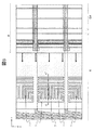
図3は、図1に示した領域AR1におけるTFT基板の概略構成を拡大して示した模式平面図である。図4は、図3のB−B’線における模式断面図である。 FIG. 3 is a schematic plan view showing an enlarged schematic configuration of the TFT substrate in the area AR1 shown in FIG. FIG. 4 is a schematic cross-sectional view taken along the line B-B ′ of FIG. 3.
本実施例の液晶表示パネルにおいて、TFT基板1のゲート辺1aの近くにある表示領域の外周付近を拡大してみると、たとえば、図3および図4に示すように、2本の隣接する走査信号線GLと2本の隣接する映像信号線DLで囲まれた画素領域が2次元的に配置されている表示領域DAの外側に、たとえば、映像信号線DLと同時に形成されるコモンバスライン5Aが設けられている。このとき、コモンバスライン5Aは、ガラス基板SUBの表面に第1の絶縁層PAS1を介して設けられている。なお、第1の絶縁層PAS1は、表示領域DAにおいて走査信号線GLと映像信号線DLの間に介在する絶縁層であり、コモンバスライン5Aと走査信号線GLが交差する領域では、コモンバスライン5Aと走査信号線GLの間に介在している。
In the liquid crystal display panel of the present embodiment, when the vicinity of the outer periphery of the display region near the
また、コモンバスライン5Aの上には、第2の絶縁層PAS2および導電層6が設けられている。このとき、第2の絶縁層PAS2には、たとえば、図3に示すようなスルーホールTH1が設けられており、導電層6は、スルーホールTH1によってコモンバスライン5Aと電気的に接続されている。また、導電層6は、スルーホールTH2によって、たとえば、走査信号線と並行する共通信号線CLまたは保持容量線などと電気的に接続されている。また、導電層6は、画素領域に形成される画素電極と同じ透明電極材料で形成されており、たとえば、ITOで形成されている。
A second insulating layer PAS2 and a
また、本実施例の液晶表示パネルにおいて、TFT基板1は、図3および図4に示すように、コモンバスライン5Aの上の第2の絶縁層PAS2に、スルーホールTH1,TH2とは別の凹溝7が設けられており、凹溝7の表面は、導電層6によって覆われている。このとき、凹溝7は、たとえば、図3に示すように、表示領域DAの外周に沿った方向(y方向)に長く延びる溝や、y方向と直交するx方向に折れ曲がったり、分岐したりする溝からなる。また、凹溝7は、2本の隣接する走査信号線GLの間に形成される溝のパターンを1つの単位にして、2本の隣接する走査信号線GLの間毎にそのパターンを形成している。
Further, in the liquid crystal display panel of the present embodiment, the
図5および図6は、本実施例の液晶表示パネルの作用効果を説明するための模式図である。
図5は、配向膜を印刷したときの材料の広がりを説明するための模式平面図である。図6は、図5のC−C’線でみた模式断面図である。なお、図5は、図1に示した領域AR1におけるTFT基板の概略構成を拡大して示した模式平面図である。
5 and 6 are schematic diagrams for explaining the operational effects of the liquid crystal display panel of this embodiment.
FIG. 5 is a schematic plan view for explaining the spread of the material when the alignment film is printed. FIG. 6 is a schematic cross-sectional view taken along the line CC ′ of FIG. FIG. 5 is a schematic plan view showing an enlarged schematic configuration of the TFT substrate in the area AR1 shown in FIG.
本実施例の液晶表示パネルにおいて、TFT基板1に配向膜を形成するときには、たとえば、インクジェット印刷法などを用いて、表示領域DAおよびその周辺のわずかな領域のみに液状の樹脂材料を印刷し、焼成する。このとき、インクジェット印刷法を用いて印刷した液状の樹脂材料は、たとえば、図5に示すように、印刷した液状の樹脂材料が表示領域DAから外側に向かう方向に濡れ広がる。またこのとき、従来のTFT基板1の場合、ゲート辺1aに近い領域では、走査信号線GLの延在方向に沿って液状の樹脂材料8が濡れ広がりやすく、シール材3を配置する領域まで達してしまうことがあった。
In the liquid crystal display panel of the present embodiment, when forming the alignment film on the
しかしながら、本実施例のTFT基板1の場合、印刷した液状の樹脂材料8が表示領域DAからゲート辺1aに向かう方向に濡れ広がるときに、シール材3を配置する領域に達する前に、第2の絶縁層PAS2の凹溝7および導電層6で構成される溝部を通る。このとき、濡れ広がって溝部に達した液状の樹脂材料8は、図6に示すように、その一部が、溝部に流れ込む。またこのとき、液状の樹脂材料8はITO膜に対する濡れ性が低いので、溝部の表面にITOで形成した導電層6を設けておくと、溝部において液状の樹脂材料8の濡れ広がりを止めることができる。
However, in the case of the
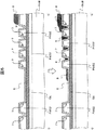
図7は、図1に示した領域AR2におけるTFT基板の概略構成を拡大して示した模式平面図である。図8は、図7に示した領域AR3の概略構成を拡大して示した模式平面図である。図9は、図8のD−D’線における模式断面図である。図10は、図7に示した領域AR4の概略構成を拡大して示した模式平面図である。図11は、図10のE−E’線における模式断面図である。 FIG. 7 is a schematic plan view showing an enlarged schematic configuration of the TFT substrate in the area AR2 shown in FIG. FIG. 8 is a schematic plan view showing an enlarged schematic configuration of the area AR3 shown in FIG. FIG. 9 is a schematic cross-sectional view taken along the line D-D ′ of FIG. 8. FIG. 10 is a schematic plan view showing an enlarged schematic configuration of the area AR4 shown in FIG. FIG. 11 is a schematic cross-sectional view taken along the line E-E ′ of FIG. 10.
本実施例の液晶表示パネルにおいて、TFT基板1のドレイン辺1cの近くにある表示領域の外周部を拡大してみると、たとえば、図10に示すように、表示領域DAの外側に、表示領域DAの外周に沿ってコモンバスライン5Bが設けられている。このコモンバスライン5Bは、走査信号線GLと同時に形成されており、コモンバスライン5Bと映像信号線DLの間には第1の絶縁層PAS1が介在している。
In the liquid crystal display panel of the present embodiment, when the outer peripheral portion of the display area near the drain side 1c of the
また、表示領域DAから見て、コモンバスライン5Bの外側にあり、かつ、映像信号線DLを集線している領域には、たとえば、図7乃至図9に示すように、保護ダイオードが形成されている領域PDsがある。このとき、保護ダイオードが形成された領域PDsには、たとえば、図8および図9に示すように、領域PDs1にある保護ダイオード用の共通線(導電層)PDs1の外側(ドレイン辺1c側)において第2の絶縁層PAS2を開口して形成した凹溝7と、凹溝7を覆う導電層6により構成された溝部を設ける。
Further, when viewed from the display area DA, it is outside the
また、液晶表示パネルのドレイン辺1cには、たとえば、図7に示したように、コモンバスライン5Bにコモン電圧を加えるためのコモン入力パターン9が設けられている。このコモン入力パターン9は、走査信号線GLと同時に形成されている。コモン入力パターン9が設けられた領域には、たとえば、図10および図11に示すように、第2の絶縁層PAS2および第1の絶縁層PAS1を開口してコモン入力パターン9に達する凹溝7と、凹溝7を覆う導電層6により構成された溝部を設ける。
Further, for example, as shown in FIG. 7, a common input pattern 9 for applying a common voltage to the
図12は、配向膜を印刷したときの材料の広がりを説明するための模式断面図である。なお、図12は、図9と同じ断面でみた図である。 FIG. 12 is a schematic cross-sectional view for explaining the spread of the material when the alignment film is printed. Note that FIG. 12 is a view seen in the same cross section as FIG.
TFT基板1に配向膜を形成する際に、たとえば、インクジェット印刷法を用いて表示領域およびその周辺のわずかな領域のみに液状の樹脂材料を印刷すると、その液状の樹脂8は、表示領域から外側に向かう方向に概ね等方的に濡れ広がる。そのため、液状の樹脂材料8は、表示領域DAからドレイン辺1cに向かう方向にも濡れ広がる。
When the alignment film is formed on the
しかしながら、本実施例のTFT基板1の場合、印刷した液状の樹脂材料8が表示領域DAからドレイン辺1cに向かう方向に濡れ広がるときにも、シール材3を配置する領域に達する前に、第2の絶縁層PAS2の凹溝7および導電層6で構成される溝部を通る。このとき、濡れ広がって溝部に達した液状の樹脂材料8は、図12に示すように、その一部が、溝部に流れ込む。またこのとき、液状の樹脂材料8はITO膜に対する濡れ性が低いので、溝部の表面にITOで形成した導電層6を設けておくと、溝部において液状の樹脂材料8の濡れ広がりを止めることができる。
However, in the case of the
図13は、TFT基板のドレイン辺に設ける溝部の変形例を説明するための模式平面図である。図14は、図13のF−F’線における模式断面図である。 FIG. 13 is a schematic plan view for explaining a modification of the groove provided on the drain side of the TFT substrate. FIG. 14 is a schematic cross-sectional view taken along the line F-F ′ of FIG. 13.
図10および図11に示した例では、コモン入力パターン9が、いわゆるベタパターンであり、溝部の周囲において第2の絶縁層PAS2の表面が平坦である。そのため、溝部だけでは液状の樹脂材料8の濡れ広がりを止められない可能性がある。
In the example shown in FIGS. 10 and 11, the common input pattern 9 is a so-called solid pattern, and the surface of the second insulating layer PAS2 is flat around the groove. Therefore, there is a possibility that wetting and spreading of the
そのため、本実施例のTFT基板1では、たとえば、図13および図14に示すように、コモン入力パターン9にスリットSLを入れることが望ましい。このように、スリットSLを入れると、たとえば、図14に示すように、コモン入力パターン9が介在している箇所と介在していない箇所で段差が生じ、液状の樹脂材料8の濡れ広がりを抑制することができる。
For this reason, in the
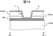
図15は、図1に示した領域AR5におけるTFT基板の概略構成を拡大して示した模式平面図である。図16は、図15のG−G’線およびH−H’線における模式断面図である。 FIG. 15 is a schematic plan view showing an enlarged schematic configuration of the TFT substrate in the area AR5 shown in FIG. 16 is a schematic cross-sectional view taken along lines G-G ′ and H-H ′ of FIG. 15.
これまでの説明では、TFT基板1のゲート辺1aおよびドレイン辺1cの近傍における液状の樹脂材料8の濡れ広がりを制御する方法について説明した。そこで、次に、TFT基板1の反ゲート辺1bおよび反ドレイン辺1dの近傍における液状の樹脂材料8の濡れ広がりを制御する方法について説明する。
In the above description, the method for controlling the wetting and spreading of the
TFT基板1の反ゲート辺1bおよび反ドレイン辺1dが接する角部は、たとえば、図15に示すように、表示領域DAの外側に、表示領域DAの外周に沿ってコモンバスライン5Bが配置されている。このコモンバスライン5Bは、たとえば、走査信号線GLと同時に形成され、図16に示すように、ガラス基板SUBと第1の絶縁層PAS1の間に配置される。
For example, as shown in FIG. 15, the corner portion where the
また、コモンバスライン5Bのうちの、反ゲート辺1bに沿った部分の上には、反ゲート辺1bに沿った方向に長く延びる溝部が設けられ、反ドレイン辺1dに沿った部分の上には、反ドレイン辺1dに沿った方向に長く延びる溝部が設けられており、これら2つの溝部は、コモンバスライン5Bの角部において連続している。
Further, a groove portion extending in the direction along the
また、反ゲート辺1bおよび反ドレイン辺1dに沿って設けられる溝部は、たとえば、図16に示すように、コモンバスライン5Bの上に積層された第1の絶縁層PAS1および第2の絶縁層PAS2を開口して形成した凹溝7と、凹溝7を覆う導電層6により構成される。このとき、凹溝7の反ゲート辺1bに沿った方向の長さは、複数本の走査信号線のうちの最外側に配置される2本の走査信号線の間隔よりも長くすることが望ましい。同様に、凹溝7の反ドレイン辺1bに沿った方向の長さは、複数本の映像信号線のうちの最外側に配置される2本の映像信号線の間隔よりも長くすることが望ましい。またこのとき、導電層6は、たとえば、図15に示すように、平面でみてコモンバスライン5B全体を覆うように形成する。
Further, the grooves provided along the
このようにすれば、印刷した液状の樹脂材料8が表示領域DAから反ゲート辺1bや反ドレイン辺1dに向かう方向に濡れ広がるときにも、シール材3を配置する領域に達する前に、第2の絶縁層PAS2および第1の絶縁層PAS1を開口した凹溝7および導電層6で構成される溝部を通る。そのため、濡れ広がって溝部に達した液状の樹脂材料8は、その一部が溝部に流れ込む。またこのとき、液状の樹脂材料8はITO膜に対する濡れ性が低いので、溝部の表面にITOで形成した導電層6を設けておくと、溝部において液状の樹脂材料8の濡れ広がりを止めることができる。
In this way, even when the printed
また、図15に示した例では、1つの溝部を設けているが、これに限らず、表示領域DAからシール材3を配置する領域に向かって2重、3重の溝部が設けられていてもよいことはもちろんである。
Further, in the example shown in FIG. 15, one groove portion is provided. However, the present invention is not limited to this, and double and triple groove portions are provided from the display area DA toward the area where the sealing
図17は、TFT基板の反ゲート辺および反ドレイン辺に設ける溝部の第1の変形例を説明するための模式断面図である。図18は、TFT基板の反ゲート辺および反ドレイン辺に設ける溝部の第2の変形例を説明するための模式断面図である。図19は、TFT基板の反ゲート辺および反ドレイン辺に設ける溝部の第3の変形例を説明するための模式断面図である。 FIG. 17 is a schematic cross-sectional view for explaining a first modification of the groove provided on the anti-gate side and the anti-drain side of the TFT substrate. FIG. 18 is a schematic cross-sectional view for explaining a second modification of the groove provided on the anti-gate side and anti-drain side of the TFT substrate. FIG. 19 is a schematic cross-sectional view for explaining a third modification of the groove provided on the anti-gate side and the anti-drain side of the TFT substrate.
図15および図16では、平面でみてコモンバスライン5B全体を覆うように導電層6を形成した場合を例に挙げているが、これに限らず、たとえば、図17に示すように、第1の絶縁層PAS1および第2の絶縁層PAS2を開口して形成した凹溝7の周辺のみに導電層6を設けてもよいことはもちろんである。
15 and 16 exemplify the case where the
また、図15および図16では、走査信号線GLと同時にコモンバスライン5Bを形成した場合を例に挙げているが、これに限らず、たとえば、映像信号線と同時にコモンバスライン5Bを形成してもよいことはもちろんである。この場合、溝部は、たとえば、図18に示すように、第2の絶縁層PAS2を開口して形成した溝部7とその表面の導電層6により構成される。またこのとき、たとえば、図19に示すように、溝部7の周辺のみに導電層6を設けてもよい。
15 and 16 show an example in which the
以上説明したように、本実施例によれば、TFT基板1において、シール材3が配置される領域よりも内側であり、かつ、表示領域DAの外側である概略環状の領域に、絶縁層を開口して設けた凹溝7と凹溝7の側面および底面に延在する導電層6で構成される溝部を設けることで、液晶表示パネルの配向膜の、表示領域の外側での濡れ広がりを抑制し、かつ、表示領域内における膜厚の均一性を維持することができる。
As described above, according to the present embodiment, in the
図20乃至図22は、本実施例の液晶表示パネルの表示領域に形成される1画素の一構成例を示す模式図である。
図20は、TFT基板の表示領域を観察者側から見たときの1画素の一構成例を示す模式平面図である。図21は、図20のJ−J’線における模式断面図である。図22は、図20のK−K’線における模式断面図である。
20 to 22 are schematic views showing one configuration example of one pixel formed in the display area of the liquid crystal display panel of this embodiment.
FIG. 20 is a schematic plan view showing a configuration example of one pixel when the display area of the TFT substrate is viewed from the observer side. FIG. 21 is a schematic cross-sectional view taken along line JJ ′ of FIG. FIG. 22 is a schematic cross-sectional view taken along the line KK ′ of FIG.
本実施例の液晶表示パネルが、ISP方式と呼ばれる横電界駆動方式の場合、TFT基板1に画素電極および対向電極が設けられている。また、IPS方式には、たとえば、平面でみた形状がくし歯状の画素電極および対向電極を同じ層、すなわち同じ絶縁層の上に配置したものと、絶縁層を介して平行に配置したものがある。このうち、絶縁層を介して画素電極と対向電極を並行に配置したIPS方式の場合、TFT基板の1画素の構成は、たとえば、図20乃至図22に示すような構成になっている。
When the liquid crystal display panel of this embodiment is a lateral electric field driving method called an ISP method, a pixel electrode and a counter electrode are provided on the
まず、TFT基板1のガラス基板SUBの表面には、x方向に延在する複数本の走査信号線GL、各走査信号線GLと並行して配置された共通信号線CL、共通信号線CLと接続した対向電極CTが設けられている。このとき、各共通信号線CLは、たとえば、図3に示したように、表示領域DAの外側において、コモンバスライン5Aに接続されている。またこのとき、各走査信号線GLからみて、共通信号線CLが配置された方向と反対側には、対向電極CTに接続された共通接続パッドCPが設けられている。
First, on the surface of the glass substrate SUB of the
そして、走査信号線GL、対向電極CTなどの上には、第1の絶縁層PAS1を介して半導体層SC、映像信号線DL、ドレイン電極SD1、ソース電極SD2が設けられている。このとき、半導体層SCは、たとえば、アモルファスシリコン(a−Si)で形成されており、TFT素子のチャネル層として機能するものの他に、たとえば、走査信号線GLと映像信号線DLが立体的に交差する箇所における走査信号線GLと映像信号線DLの短絡を防ぐためのものなどが形成されている。またこのとき、TFT素子のチャネル層として機能する半導体層SCは、走査信号線GLの上に第1の絶縁層PAS1を介して設けられており、走査信号線GLと半導体層SCの間に介在する第1の絶縁膜PAS1が、TFT素子のゲート絶縁膜として機能する。 A semiconductor layer SC, a video signal line DL, a drain electrode SD1, and a source electrode SD2 are provided on the scanning signal line GL, the counter electrode CT, and the like via a first insulating layer PAS1. At this time, the semiconductor layer SC is formed of, for example, amorphous silicon (a-Si), and in addition to the one that functions as a channel layer of the TFT element, for example, the scanning signal line GL and the video signal line DL are three-dimensionally formed. In order to prevent a short circuit between the scanning signal line GL and the video signal line DL at the intersection, a line is formed. At this time, the semiconductor layer SC functioning as the channel layer of the TFT element is provided on the scanning signal line GL via the first insulating layer PAS1, and is interposed between the scanning signal line GL and the semiconductor layer SC. The first insulating film PAS1 functions as a gate insulating film of the TFT element.
また、映像信号線DLは、y方向に延在する信号線であり、その一部が分岐してTFT素子のチャネル層として機能する半導体層SC上に設けられている。この映像信号線DLから分岐した部分がドレイン電極SD1である。 The video signal line DL is a signal line extending in the y direction, and a part of the video signal line DL is provided on the semiconductor layer SC that branches and functions as a channel layer of the TFT element. A portion branched from the video signal line DL is a drain electrode SD1.
そして、半導体層SC、映像信号線DLなどの上には、第2の絶縁層PAS2を介して画素電極PXおよびブリッジ配線BRが設けられている。画素電極PXは、スルーホールTH3によりソース電極SD2と電気的に接続されている。また、画素電極PXは、平面でみて対向電極CTと重なる領域に複数本のスリット(開口部)SLが設けられている。 A pixel electrode PX and a bridge wiring BR are provided on the semiconductor layer SC, the video signal line DL, etc. via a second insulating layer PAS2. The pixel electrode PX is electrically connected to the source electrode SD2 through the through hole TH3. In addition, the pixel electrode PX is provided with a plurality of slits (openings) SL in a region overlapping the counter electrode CT when viewed in plan.
また、ブリッジ配線BRは、1本の走査信号線GLを挟んで配置される2つの対向電極CTを電気的に接続する配線であり、スルーホールTH4,TH5により、走査信号線GLを挟んで配置される共通信号線CLおよび共通接続パッドCPと電気的に接続されている。 The bridge wiring BR is a wiring for electrically connecting two counter electrodes CT arranged with one scanning signal line GL interposed therebetween, and is arranged with the scanning signal line GL interposed between the through holes TH4 and TH5. Are electrically connected to the common signal line CL and the common connection pad CP.
なお、本発明に関わる液晶表示パネルにおけるTFT基板1は、1画素の構成がある特定の構成のものに限定されるわけではなく、従来から一般に知られている種々の構成のTFT基板に適用することができるのはもちろんである。
Note that the
以上、本発明を、前記実施例に基づき具体的に説明したが、本発明は、前記実施例に限定されるものではなく、その要旨を逸脱しない範囲において、種々変更可能であることはもちろんである。 The present invention has been specifically described above based on the above-described embodiments. However, the present invention is not limited to the above-described embodiments, and various modifications can be made without departing from the scope of the present invention. is there.
たとえば、前記実施例では、液晶表示パネルのTFT基板1に、配向膜の濡れ広がりを抑制する溝部を設ける例を説明した。しかしながら、本発明は、TFT基板1に限らず、たとえば、対向基板にも適用できることはもちろんである。
For example, in the above-described embodiment, an example has been described in which the
液晶表示パネルが、TN方式やVA方式の縦電界駆動方式の場合、対向電極CTは対向基板2に設けられる。このとき、対向基板2は、たとえば、ガラス基板の表面にブラックマトリクス(遮光パターン)やカラーフィルタが設けられ、それらの上にオーバーコート層を介して対向電極が設けられている。そのため、たとえば、オーバーコート層を形成するときに、シール材3が配置される領域よりも内側であり、かつ、表示領域の外側である領域にオーバーコート層を開口した凹溝を形成し、その凹溝の表面に対向電極を延在させて溝部を形成すれば、該溝部で配向膜の濡れ広がりを止めることができる。
When the liquid crystal display panel is a TN type or VA type vertical electric field driving method, the counter electrode CT is provided on the counter substrate 2. At this time, for example, the counter substrate 2 is provided with a black matrix (light-shielding pattern) and a color filter on the surface of a glass substrate, and a counter electrode is provided thereon via an overcoat layer. Therefore, for example, when the overcoat layer is formed, a concave groove having an overcoat layer is formed in a region that is inside the region where the sealing
1…TFT基板
2…対向基板
3…シール材
4…液晶材料
5A,5B…コモンバスライン
6…導電膜(ITO膜)
7…凹溝
8…液状の樹脂材料(配向膜)
9…コモン入力パターン
GL…走査信号線
DL…映像信号線
SD1…ドレイン電極
SD2…ソース電極
SC…チャネル層(半導体層)
PX…画素電極
CT…対向電極
PAS1…第1の絶縁層
PAS2…第2の絶縁層
CL…共通信号線
CP…共通接続パッド
TH1,TH2,TH3,TH4,TH5…スルーホール
DESCRIPTION OF
7: Groove 8: Liquid resin material (alignment film)
9 ... Common input pattern GL ... Scanning signal line DL ... Video signal line SD1 ... Drain electrode SD2 ... Source electrode SC ... Channel layer (semiconductor layer)
PX ... pixel electrode CT ... counter electrode PAS1 ... first insulating layer PAS2 ... second insulating layer CL ... common signal line CP ... common connection pad TH1, TH2, TH3, TH4, TH5 ... through hole
Claims (10)
前記一対の基板は、相対する基板と対向する面の表面に配向膜を有し、
前記一対の基板のうちの少なくとも一方の基板は、前記シール材が配置される領域よりも内側であり、かつ、前記表示領域の外側である環状の領域において、前記配向膜と前記基板との間に、第1の導電層および第2の導電層と、前記第1の導電層と前記第2の導電層との間に介在する絶縁層とを有し、
前記絶縁層は、少なくとも前記表示領域の外周に沿った方向に延設され、かつ、前記配向膜側が開口した凹溝を有し、
前記第1の導電層は、前記凹溝の形状に沿って形成されていることを特徴とする液晶表示装置。 An annular sealing material is disposed between the pair of substrates, and a liquid crystal material is sealed in a space surrounded by the pair of substrates and the sealing material, and in a region where the pair of substrates and the liquid crystal material overlap in a plan view. A liquid crystal display device having a display panel in which a display area is configured,
The pair of substrates has an alignment film on a surface facing the opposite substrate,
At least one of the pair of substrates is between the alignment film and the substrate in an annular region that is inside the region where the sealant is disposed and outside the display region. A first conductive layer and a second conductive layer, and an insulating layer interposed between the first conductive layer and the second conductive layer,
The insulating layer has a groove that extends at least in the direction along the outer periphery of the display region and has an opening on the alignment film side ,
The liquid crystal display device, wherein the first conductive layer is formed along the shape of the concave groove .
前記第1の導電層は、前記画素電極と同じ材料でなることを特徴とする請求項1に記載の液晶表示装置。 The substrate having the insulating layer includes a plurality of scanning signal lines, a plurality of video signal lines sterically intersecting with the plurality of scanning signal lines, a plurality of TFT elements disposed in the display region, and A plurality of pixel electrodes;
The liquid crystal display device according to claim 1, wherein the first conductive layer is made of the same material as the pixel electrode.
前記走査信号線は、前記環状領域の一辺において、前記表示領域から前記シール材へ向かう方向で前記環状領域を横断しており、
前記凹溝は、前記環状領域内の前記走査信号線の間毎に設けられていることを特徴とする請求項2に記載の液晶表示装置。 The annular region has a rectangular outer periphery and inner periphery,
The scanning signal line crosses the annular region in a direction from the display region to the sealing material on one side of the annular region,
The liquid crystal display device according to claim 2, wherein the concave groove is provided between the scanning signal lines in the annular region .
前記映像信号線は、前記環状領域の一辺において、前記表示領域から前記シール材へ向かう方向で前記環状領域を横断しており、
前記凹溝は、前記環状領域内の前記映像信号線の間毎に設けられていることを特徴とする請求項2に記載の液晶表示装置。 The annular region has a rectangular outer periphery and inner periphery,
The video signal line crosses the annular region in a direction from the display region to the sealing material on one side of the annular region,
Before SL grooves, the liquid crystal display device according to claim 2, characterized in that provided for each between the video signal line of the annular area.
前記保護ダイオードは、前記環状領域内に、前記表示領域に沿って形成されていることを特徴とする請求項2に記載の液晶表示装置。 The second conductive layer forms part of a protective diode;
The liquid crystal display device according to claim 2 , wherein the protection diode is formed in the annular region along the display region .
前記第2の導電層は、前記共通電極に電気信号を供給するコモンバスラインであり、
前記コモンバスラインは、前記環状領域内に、前記表示領域に沿って形成されていることを特徴とする請求項2に記載の液晶表示装置。 The substrate having the insulating layer has a common electrode disposed in the display region,
The second conductive layer is a common bus line that supplies an electric signal to the common electrode,
The liquid crystal display device according to claim 2 , wherein the common bus line is formed in the annular area along the display area .
前記走査信号線は、前記環状領域の一辺において、前記表示領域から前記シール材へ向かう方向で前記環状領域を横断しており、The scanning signal line crosses the annular region in a direction from the display region to the sealing material on one side of the annular region,
前記映像信号線は、前記環状領域の他の一辺において、前記表示領域から前記シール材へ向かう方向で前記環状領域を横断しており、The video signal line crosses the annular region in a direction from the display region to the sealing material on the other side of the annular region,
前記環状領域の前記走査信号線および前記映像信号線が横断していない辺において、前記凹溝は、前記コモンバスライン上に、前記表示領域に沿って延設置されていることを特長とする請求項7に記載の液晶表示装置。The groove is extended along the display area on the common bus line at a side of the annular area where the scanning signal line and the video signal line do not cross. Item 8. A liquid crystal display device according to item 7.
Priority Applications (5)
| Application Number | Priority Date | Filing Date | Title |
|---|---|---|---|
| JP2006151478A JP4651580B2 (en) | 2006-05-31 | 2006-05-31 | Liquid crystal display device |
| US11/798,278 US7639334B2 (en) | 2006-05-31 | 2007-05-11 | Liquid crystal display device |
| TW096117438A TW200801677A (en) | 2006-05-31 | 2007-05-16 | Liquid crystal display device |
| KR1020070047698A KR100861433B1 (en) | 2006-05-31 | 2007-05-16 | Liquid Crystal Display Device |
| CN2007101054352A CN101082745B (en) | 2006-05-31 | 2007-05-30 | Liquid crystal display device |
Applications Claiming Priority (1)
| Application Number | Priority Date | Filing Date | Title |
|---|---|---|---|
| JP2006151478A JP4651580B2 (en) | 2006-05-31 | 2006-05-31 | Liquid crystal display device |
Publications (3)
| Publication Number | Publication Date |
|---|---|
| JP2007322627A JP2007322627A (en) | 2007-12-13 |
| JP2007322627A5 JP2007322627A5 (en) | 2008-12-25 |
| JP4651580B2 true JP4651580B2 (en) | 2011-03-16 |
Family
ID=38789640
Family Applications (1)
| Application Number | Title | Priority Date | Filing Date |
|---|---|---|---|
| JP2006151478A Active JP4651580B2 (en) | 2006-05-31 | 2006-05-31 | Liquid crystal display device |
Country Status (5)
| Country | Link |
|---|---|
| US (1) | US7639334B2 (en) |
| JP (1) | JP4651580B2 (en) |
| KR (1) | KR100861433B1 (en) |
| CN (1) | CN101082745B (en) |
| TW (1) | TW200801677A (en) |
Families Citing this family (42)
| Publication number | Priority date | Publication date | Assignee | Title |
|---|---|---|---|---|
| JP2006201312A (en) * | 2005-01-18 | 2006-08-03 | Nec Corp | Liquid crystal display panel and liquid crystal display device |
| US8400597B2 (en) * | 2008-06-20 | 2013-03-19 | Sharp Kabushiki Kaisha | Liquid crystal display device |
| US20110255041A1 (en) * | 2008-12-17 | 2011-10-20 | Tomohiro Inoue | Liquid crystal panel and liquid crystal display device |
| CN101825817B (en) * | 2009-03-06 | 2011-12-14 | 北京京东方光电科技有限公司 | Liquid crystal display |
| CN102687066A (en) * | 2010-01-12 | 2012-09-19 | 夏普株式会社 | Liquid crystal display device and manufacturing method therefor |
| BR112012014142A2 (en) | 2010-01-14 | 2016-08-16 | Sharp Kabushiki Kaisaha | liquid crystal display device |
| US8913221B2 (en) | 2010-04-16 | 2014-12-16 | Sharp Kabushiki Kaisha | Display device |
| JP5285809B2 (en) | 2010-04-19 | 2013-09-11 | シャープ株式会社 | Display device and manufacturing method thereof |
| JP5517726B2 (en) * | 2010-04-23 | 2014-06-11 | 株式会社ジャパンディスプレイ | Liquid crystal display |
| JP5302460B2 (en) * | 2010-06-10 | 2013-10-02 | シャープ株式会社 | Liquid crystal display device and manufacturing method thereof |
| CN103097941A (en) | 2010-11-30 | 2013-05-08 | 株式会社东芝 | Refractive index distribution liquid crystal optical element and image display device |
| CN104335111B (en) | 2012-05-25 | 2017-03-29 | 夏普株式会社 | Liquid crystal indicator |
| CN103576390A (en) * | 2012-08-01 | 2014-02-12 | 立景光电股份有限公司 | Display |
| WO2014038159A1 (en) * | 2012-09-04 | 2014-03-13 | シャープ株式会社 | Liquid crystal display device |
| KR20140062669A (en) * | 2012-11-14 | 2014-05-26 | 삼성디스플레이 주식회사 | Display panel and manufacturing method of the same |
| WO2014083807A1 (en) * | 2012-11-28 | 2014-06-05 | シャープ株式会社 | Liquid crystal display device |
| CN103018980A (en) * | 2012-12-31 | 2013-04-03 | 信利半导体有限公司 | Wide-viewing-angle liquid crystal display and display method thereof |
| WO2015075972A1 (en) * | 2013-11-21 | 2015-05-28 | シャープ株式会社 | Display device |
| CN103676342B (en) * | 2013-12-27 | 2015-12-09 | 深圳市华星光电技术有限公司 | The fanout area structure of narrow frame liquid crystal display |
| WO2015170369A1 (en) | 2014-05-09 | 2015-11-12 | パナソニック液晶ディスプレイ株式会社 | Liquid crystal display device |
| CN104122727B (en) * | 2014-07-29 | 2017-02-22 | 深圳市华星光电技术有限公司 | Array substrate and liquid crystal display panel |
| CN104216189B (en) * | 2014-09-26 | 2017-04-19 | 南京中电熊猫液晶显示科技有限公司 | Liquid crystal display panel and manufacturing method thereof |
| JP6602610B2 (en) * | 2014-09-26 | 2019-11-06 | 芝浦メカトロニクス株式会社 | Substrate, film-forming substrate manufacturing method and coating apparatus |
| JP2016109807A (en) | 2014-12-04 | 2016-06-20 | 株式会社ジャパンディスプレイ | Liquid crystal display device |
| CN104765214B (en) * | 2015-03-26 | 2018-09-18 | 京东方科技集团股份有限公司 | TFT substrate and its manufacturing method, display device |
| CN104777650B (en) * | 2015-04-22 | 2018-10-30 | 京东方科技集团股份有限公司 | Tft array substrate, its production method, liquid crystal display panel and display device |
| KR102366768B1 (en) * | 2015-07-07 | 2022-02-22 | 엘지디스플레이 주식회사 | Liquid crystal display device |
| KR102436650B1 (en) * | 2015-11-02 | 2022-08-26 | 삼성디스플레이 주식회사 | Display device and manufacturing method thereof |
| KR102487276B1 (en) | 2016-03-21 | 2023-01-12 | 삼성디스플레이 주식회사 | Inkjet printing method and display device manufacturing method using the inkjet printing method |
| KR20180047587A (en) | 2016-10-31 | 2018-05-10 | 엘지디스플레이 주식회사 | Organic light emitting diode display |
| KR20180052150A (en) * | 2016-11-09 | 2018-05-18 | 삼성디스플레이 주식회사 | Liquid crystal display device |
| CN106501983B (en) * | 2016-12-23 | 2019-08-02 | 厦门天马微电子有限公司 | Array substrate, display panel and display device |
| CN107765484B (en) * | 2017-11-07 | 2019-11-05 | 惠科股份有限公司 | Array substrate and its display panel of application |
| CN108508657B (en) * | 2018-04-12 | 2023-07-25 | 京东方科技集团股份有限公司 | Manufacturing method and application of alignment film |
| KR20190124845A (en) * | 2018-04-26 | 2019-11-06 | 삼성디스플레이 주식회사 | Display device and method for manufacturing display device |
| JP7150523B2 (en) * | 2018-08-22 | 2022-10-11 | 株式会社ジャパンディスプレイ | Display device |
| CN109001949A (en) * | 2018-09-11 | 2018-12-14 | 惠科股份有限公司 | Array substrate and display panel |
| CN109324453A (en) * | 2018-09-30 | 2019-02-12 | 惠科股份有限公司 | A kind of display panel and display device |
| CN109613775B (en) * | 2019-01-16 | 2020-11-24 | 惠科股份有限公司 | Array substrate and display device |
| CN109765719A (en) * | 2019-03-21 | 2019-05-17 | 深圳市华星光电技术有限公司 | The production method and substrate of substrate |
| CN110176463A (en) * | 2019-05-24 | 2019-08-27 | 深圳市华星光电技术有限公司 | Substrate and preparation method |
| WO2024011597A1 (en) * | 2022-07-15 | 2024-01-18 | 京东方科技集团股份有限公司 | Display panel and display apparatus |
Citations (9)
| Publication number | Priority date | Publication date | Assignee | Title |
|---|---|---|---|---|
| JPH1073835A (en) * | 1996-08-30 | 1998-03-17 | Casio Comput Co Ltd | Liquid crystal cell and its production |
| JPH10268335A (en) * | 1997-03-27 | 1998-10-09 | Semiconductor Energy Lab Co Ltd | Contact structure |
| JPH11160734A (en) * | 1997-11-28 | 1999-06-18 | Semiconductor Energy Lab Co Ltd | Liquid crystal electrooptical device |
| JP2001330837A (en) * | 2000-05-19 | 2001-11-30 | Matsushita Electric Ind Co Ltd | Hermetic structural, its manufacturing method, liquid crystal display device using the same and its manufacturing method |
| JP2001337316A (en) * | 2000-05-26 | 2001-12-07 | Seiko Epson Corp | Method for forming protective layer, method for forming alignment layer, liquid crystal device and electronic equipment |
| JP2004272272A (en) * | 2004-03-30 | 2004-09-30 | Semiconductor Energy Lab Co Ltd | Contact structure and active matrix type display apparatus |
| JP2005221890A (en) * | 2004-02-06 | 2005-08-18 | Sharp Corp | Forming method and forming apparatus for alignment layer |
| JP2006010856A (en) * | 2004-06-23 | 2006-01-12 | Seiko Epson Corp | Substrate for optoelectronic device and optoelectronic device, and electronic appliance |
| JP2007322474A (en) * | 2006-05-30 | 2007-12-13 | Hitachi Displays Ltd | Liquid crystal display device |
Family Cites Families (6)
| Publication number | Priority date | Publication date | Assignee | Title |
|---|---|---|---|---|
| JP3871764B2 (en) * | 1997-03-26 | 2007-01-24 | 株式会社半導体エネルギー研究所 | Reflective display device |
| JP4081643B2 (en) * | 2001-08-01 | 2008-04-30 | 株式会社日立製作所 | Liquid crystal display |
| KR101009668B1 (en) * | 2003-10-06 | 2011-01-19 | 엘지디스플레이 주식회사 | The liquid crystal display device and the method for fabricating the same |
| JP4768393B2 (en) * | 2005-10-21 | 2011-09-07 | Nec液晶テクノロジー株式会社 | Liquid crystal display device and manufacturing method thereof |
| JP4820226B2 (en) * | 2006-07-18 | 2011-11-24 | パナソニック液晶ディスプレイ株式会社 | Liquid crystal display |
| JP4869892B2 (en) * | 2006-12-06 | 2012-02-08 | 株式会社 日立ディスプレイズ | Liquid crystal display |
-
2006
- 2006-05-31 JP JP2006151478A patent/JP4651580B2/en active Active
-
2007
- 2007-05-11 US US11/798,278 patent/US7639334B2/en active Active
- 2007-05-16 KR KR1020070047698A patent/KR100861433B1/en active IP Right Grant
- 2007-05-16 TW TW096117438A patent/TW200801677A/en unknown
- 2007-05-30 CN CN2007101054352A patent/CN101082745B/en active Active
Patent Citations (9)
| Publication number | Priority date | Publication date | Assignee | Title |
|---|---|---|---|---|
| JPH1073835A (en) * | 1996-08-30 | 1998-03-17 | Casio Comput Co Ltd | Liquid crystal cell and its production |
| JPH10268335A (en) * | 1997-03-27 | 1998-10-09 | Semiconductor Energy Lab Co Ltd | Contact structure |
| JPH11160734A (en) * | 1997-11-28 | 1999-06-18 | Semiconductor Energy Lab Co Ltd | Liquid crystal electrooptical device |
| JP2001330837A (en) * | 2000-05-19 | 2001-11-30 | Matsushita Electric Ind Co Ltd | Hermetic structural, its manufacturing method, liquid crystal display device using the same and its manufacturing method |
| JP2001337316A (en) * | 2000-05-26 | 2001-12-07 | Seiko Epson Corp | Method for forming protective layer, method for forming alignment layer, liquid crystal device and electronic equipment |
| JP2005221890A (en) * | 2004-02-06 | 2005-08-18 | Sharp Corp | Forming method and forming apparatus for alignment layer |
| JP2004272272A (en) * | 2004-03-30 | 2004-09-30 | Semiconductor Energy Lab Co Ltd | Contact structure and active matrix type display apparatus |
| JP2006010856A (en) * | 2004-06-23 | 2006-01-12 | Seiko Epson Corp | Substrate for optoelectronic device and optoelectronic device, and electronic appliance |
| JP2007322474A (en) * | 2006-05-30 | 2007-12-13 | Hitachi Displays Ltd | Liquid crystal display device |
Also Published As
| Publication number | Publication date |
|---|---|
| TWI363211B (en) | 2012-05-01 |
| JP2007322627A (en) | 2007-12-13 |
| CN101082745A (en) | 2007-12-05 |
| US20070279565A1 (en) | 2007-12-06 |
| TW200801677A (en) | 2008-01-01 |
| KR100861433B1 (en) | 2008-10-02 |
| US7639334B2 (en) | 2009-12-29 |
| CN101082745B (en) | 2010-07-28 |
| KR20070115615A (en) | 2007-12-06 |
Similar Documents
| Publication | Publication Date | Title |
|---|---|---|
| JP4651580B2 (en) | Liquid crystal display device | |
| JP4820226B2 (en) | Liquid crystal display | |
| JP6979378B2 (en) | Display device with sensor | |
| JP6491825B2 (en) | Liquid crystal display | |
| JP2003215599A (en) | Liquid crystal display device | |
| KR102609077B1 (en) | Liquid crystal display device | |
| JP2010054980A (en) | Liquid crystal display device | |
| JP2017111396A (en) | Display device | |
| US8373828B2 (en) | Display apparatus | |
| WO2014083807A1 (en) | Liquid crystal display device | |
| JP2007322474A (en) | Liquid crystal display device | |
| US11022846B2 (en) | Substrate for display device and display device | |
| KR20150081939A (en) | Display apparatus and fabrication method of the same | |
| JP2016038520A (en) | Display device | |
| KR20080049346A (en) | Liquid crystal display panel | |
| JP5131525B2 (en) | Active matrix liquid crystal display device | |
| US10754203B2 (en) | Display panel | |
| KR101024642B1 (en) | Liquid Crystal Display Panel and Method of Fabricating the same | |
| JP6739564B2 (en) | Liquid crystal display | |
| JP5106169B2 (en) | Display element | |
| KR20090121691A (en) | Liquid crystal display device | |
| WO2020144998A1 (en) | Display device | |
| US8797489B2 (en) | Liquid crystal display panel and display apparatus using the same | |
| KR20160086013A (en) | Liquid crystal display device | |
| KR101868880B1 (en) | Electrophoretic Display Device |
Legal Events
| Date | Code | Title | Description |
|---|---|---|---|
| A521 | Request for written amendment filed |
Free format text: JAPANESE INTERMEDIATE CODE: A523 Effective date: 20081110 |
|
| A621 | Written request for application examination |
Free format text: JAPANESE INTERMEDIATE CODE: A621 Effective date: 20081110 |
|
| A977 | Report on retrieval |
Free format text: JAPANESE INTERMEDIATE CODE: A971007 Effective date: 20101102 |
|
| TRDD | Decision of grant or rejection written | ||
| A01 | Written decision to grant a patent or to grant a registration (utility model) |
Free format text: JAPANESE INTERMEDIATE CODE: A01 Effective date: 20101214 |
|
| A01 | Written decision to grant a patent or to grant a registration (utility model) |
Free format text: JAPANESE INTERMEDIATE CODE: A01 |
|
| A61 | First payment of annual fees (during grant procedure) |
Free format text: JAPANESE INTERMEDIATE CODE: A61 Effective date: 20101214 |
|
| R150 | Certificate of patent or registration of utility model |
Ref document number: 4651580 Country of ref document: JP Free format text: JAPANESE INTERMEDIATE CODE: R150 Free format text: JAPANESE INTERMEDIATE CODE: R150 |
|
| FPAY | Renewal fee payment (event date is renewal date of database) |
Free format text: PAYMENT UNTIL: 20131224 Year of fee payment: 3 |
|
| A711 | Notification of change in applicant |
Free format text: JAPANESE INTERMEDIATE CODE: A712 Effective date: 20110218 |
|
| RD03 | Notification of appointment of power of attorney |
Free format text: JAPANESE INTERMEDIATE CODE: A7423 Effective date: 20110218 |
|
| A072 | Dismissal of procedure [no reply to invitation to correct request for examination] |
Free format text: JAPANESE INTERMEDIATE CODE: A072 Effective date: 20110607 |
|
| FPAY | Renewal fee payment (event date is renewal date of database) |
Free format text: PAYMENT UNTIL: 20131224 Year of fee payment: 3 |
|
| S111 | Request for change of ownership or part of ownership |
Free format text: JAPANESE INTERMEDIATE CODE: R313115 Free format text: JAPANESE INTERMEDIATE CODE: R313121 |
|
| FPAY | Renewal fee payment (event date is renewal date of database) |
Free format text: PAYMENT UNTIL: 20131224 Year of fee payment: 3 |
|
| R350 | Written notification of registration of transfer |
Free format text: JAPANESE INTERMEDIATE CODE: R350 |
|
| R250 | Receipt of annual fees |
Free format text: JAPANESE INTERMEDIATE CODE: R250 |
|
| R250 | Receipt of annual fees |
Free format text: JAPANESE INTERMEDIATE CODE: R250 |
|
| R250 | Receipt of annual fees |
Free format text: JAPANESE INTERMEDIATE CODE: R250 |
|
| R250 | Receipt of annual fees |
Free format text: JAPANESE INTERMEDIATE CODE: R250 |
|
| R250 | Receipt of annual fees |
Free format text: JAPANESE INTERMEDIATE CODE: R250 |
|
| R250 | Receipt of annual fees |
Free format text: JAPANESE INTERMEDIATE CODE: R250 |
|
| R250 | Receipt of annual fees |
Free format text: JAPANESE INTERMEDIATE CODE: R250 |
|
| R250 | Receipt of annual fees |
Free format text: JAPANESE INTERMEDIATE CODE: R250 |
|
| S531 | Written request for registration of change of domicile |
Free format text: JAPANESE INTERMEDIATE CODE: R313531 |
|
| S533 | Written request for registration of change of name |
Free format text: JAPANESE INTERMEDIATE CODE: R313533 |
|
| R350 | Written notification of registration of transfer |
Free format text: JAPANESE INTERMEDIATE CODE: R350 |
|
| R250 | Receipt of annual fees |
Free format text: JAPANESE INTERMEDIATE CODE: R250 |
|
| R250 | Receipt of annual fees |
Free format text: JAPANESE INTERMEDIATE CODE: R250 |
|
| S111 | Request for change of ownership or part of ownership |
Free format text: JAPANESE INTERMEDIATE CODE: R313117 |
|
| R350 | Written notification of registration of transfer |
Free format text: JAPANESE INTERMEDIATE CODE: R350 |
|
| R250 | Receipt of annual fees |
Free format text: JAPANESE INTERMEDIATE CODE: R250 |