EP2525248B1 - Autostereoscopic touch-sensing display apparatus - Google Patents
Autostereoscopic touch-sensing display apparatus Download PDFInfo
- Publication number
- EP2525248B1 EP2525248B1 EP12162643.6A EP12162643A EP2525248B1 EP 2525248 B1 EP2525248 B1 EP 2525248B1 EP 12162643 A EP12162643 A EP 12162643A EP 2525248 B1 EP2525248 B1 EP 2525248B1
- Authority
- EP
- European Patent Office
- Prior art keywords
- electrode
- patterns
- pixels
- pixel
- substrate
- Prior art date
- Legal status (The legal status is an assumption and is not a legal conclusion. Google has not performed a legal analysis and makes no representation as to the accuracy of the status listed.)
- Active
Links
- 230000004888 barrier function Effects 0.000 claims description 158
- 239000000758 substrate Substances 0.000 claims description 134
- 230000005684 electric field Effects 0.000 claims description 16
- 239000003086 colorant Substances 0.000 claims description 10
- 239000004020 conductor Substances 0.000 claims description 6
- 238000001514 detection method Methods 0.000 claims description 2
- 239000010410 layer Substances 0.000 description 56
- 239000010409 thin film Substances 0.000 description 51
- 108010089894 bradykinin potentiating factors Proteins 0.000 description 11
- 239000004973 liquid crystal related substance Substances 0.000 description 8
- 239000011159 matrix material Substances 0.000 description 8
- 239000011521 glass Substances 0.000 description 4
- 239000003990 capacitor Substances 0.000 description 3
- 238000002513 implantation Methods 0.000 description 3
- 238000004519 manufacturing process Methods 0.000 description 3
- 238000000034 method Methods 0.000 description 3
- 230000037361 pathway Effects 0.000 description 3
- 230000010287 polarization Effects 0.000 description 3
- VYPSYNLAJGMNEJ-UHFFFAOYSA-N Silicium dioxide Chemical compound O=[Si]=O VYPSYNLAJGMNEJ-UHFFFAOYSA-N 0.000 description 2
- 239000012790 adhesive layer Substances 0.000 description 2
- 230000008859 change Effects 0.000 description 2
- 238000005137 deposition process Methods 0.000 description 2
- 239000010408 film Substances 0.000 description 2
- 239000000463 material Substances 0.000 description 2
- 238000005259 measurement Methods 0.000 description 2
- 230000004048 modification Effects 0.000 description 2
- 238000012986 modification Methods 0.000 description 2
- 229910052814 silicon oxide Inorganic materials 0.000 description 2
- 229910052581 Si3N4 Inorganic materials 0.000 description 1
- 229910004205 SiNX Inorganic materials 0.000 description 1
- 230000001413 cellular effect Effects 0.000 description 1
- 230000005283 ground state Effects 0.000 description 1
- 239000007943 implant Substances 0.000 description 1
- 239000011810 insulating material Substances 0.000 description 1
- 239000007788 liquid Substances 0.000 description 1
- 230000003287 optical effect Effects 0.000 description 1
- 230000002093 peripheral effect Effects 0.000 description 1
- 239000011347 resin Substances 0.000 description 1
- 229920005989 resin Polymers 0.000 description 1
- 230000004044 response Effects 0.000 description 1
- 239000003566 sealing material Substances 0.000 description 1
- 230000035945 sensitivity Effects 0.000 description 1
- HQVNEWCFYHHQES-UHFFFAOYSA-N silicon nitride Chemical compound N12[Si]34N5[Si]62N3[Si]51N64 HQVNEWCFYHHQES-UHFFFAOYSA-N 0.000 description 1
- 230000000007 visual effect Effects 0.000 description 1
Images


Classifications
-
- G—PHYSICS
- G02—OPTICS
- G02F—OPTICAL DEVICES OR ARRANGEMENTS FOR THE CONTROL OF LIGHT BY MODIFICATION OF THE OPTICAL PROPERTIES OF THE MEDIA OF THE ELEMENTS INVOLVED THEREIN; NON-LINEAR OPTICS; FREQUENCY-CHANGING OF LIGHT; OPTICAL LOGIC ELEMENTS; OPTICAL ANALOGUE/DIGITAL CONVERTERS
- G02F1/00—Devices or arrangements for the control of the intensity, colour, phase, polarisation or direction of light arriving from an independent light source, e.g. switching, gating or modulating; Non-linear optics
- G02F1/01—Devices or arrangements for the control of the intensity, colour, phase, polarisation or direction of light arriving from an independent light source, e.g. switching, gating or modulating; Non-linear optics for the control of the intensity, phase, polarisation or colour
- G02F1/13—Devices or arrangements for the control of the intensity, colour, phase, polarisation or direction of light arriving from an independent light source, e.g. switching, gating or modulating; Non-linear optics for the control of the intensity, phase, polarisation or colour based on liquid crystals, e.g. single liquid crystal display cells
- G02F1/133—Constructional arrangements; Operation of liquid crystal cells; Circuit arrangements
- G02F1/1333—Constructional arrangements; Manufacturing methods
- G02F1/13338—Input devices, e.g. touch panels
-
- G—PHYSICS
- G06—COMPUTING; CALCULATING OR COUNTING
- G06F—ELECTRIC DIGITAL DATA PROCESSING
- G06F3/00—Input arrangements for transferring data to be processed into a form capable of being handled by the computer; Output arrangements for transferring data from processing unit to output unit, e.g. interface arrangements
- G06F3/01—Input arrangements or combined input and output arrangements for interaction between user and computer
- G06F3/03—Arrangements for converting the position or the displacement of a member into a coded form
- G06F3/041—Digitisers, e.g. for touch screens or touch pads, characterised by the transducing means
- G06F3/044—Digitisers, e.g. for touch screens or touch pads, characterised by the transducing means by capacitive means
- G06F3/0448—Details of the electrode shape, e.g. for enhancing the detection of touches, for generating specific electric field shapes, for enhancing display quality
-
- G—PHYSICS
- G02—OPTICS
- G02F—OPTICAL DEVICES OR ARRANGEMENTS FOR THE CONTROL OF LIGHT BY MODIFICATION OF THE OPTICAL PROPERTIES OF THE MEDIA OF THE ELEMENTS INVOLVED THEREIN; NON-LINEAR OPTICS; FREQUENCY-CHANGING OF LIGHT; OPTICAL LOGIC ELEMENTS; OPTICAL ANALOGUE/DIGITAL CONVERTERS
- G02F1/00—Devices or arrangements for the control of the intensity, colour, phase, polarisation or direction of light arriving from an independent light source, e.g. switching, gating or modulating; Non-linear optics
- G02F1/01—Devices or arrangements for the control of the intensity, colour, phase, polarisation or direction of light arriving from an independent light source, e.g. switching, gating or modulating; Non-linear optics for the control of the intensity, phase, polarisation or colour
- G02F1/13—Devices or arrangements for the control of the intensity, colour, phase, polarisation or direction of light arriving from an independent light source, e.g. switching, gating or modulating; Non-linear optics for the control of the intensity, phase, polarisation or colour based on liquid crystals, e.g. single liquid crystal display cells
- G02F1/133—Constructional arrangements; Operation of liquid crystal cells; Circuit arrangements
- G02F1/1333—Constructional arrangements; Manufacturing methods
-
- G—PHYSICS
- G06—COMPUTING; CALCULATING OR COUNTING
- G06F—ELECTRIC DIGITAL DATA PROCESSING
- G06F3/00—Input arrangements for transferring data to be processed into a form capable of being handled by the computer; Output arrangements for transferring data from processing unit to output unit, e.g. interface arrangements
- G06F3/01—Input arrangements or combined input and output arrangements for interaction between user and computer
- G06F3/03—Arrangements for converting the position or the displacement of a member into a coded form
- G06F3/041—Digitisers, e.g. for touch screens or touch pads, characterised by the transducing means
- G06F3/0412—Digitisers structurally integrated in a display
-
- G—PHYSICS
- G06—COMPUTING; CALCULATING OR COUNTING
- G06F—ELECTRIC DIGITAL DATA PROCESSING
- G06F3/00—Input arrangements for transferring data to be processed into a form capable of being handled by the computer; Output arrangements for transferring data from processing unit to output unit, e.g. interface arrangements
- G06F3/01—Input arrangements or combined input and output arrangements for interaction between user and computer
- G06F3/03—Arrangements for converting the position or the displacement of a member into a coded form
- G06F3/041—Digitisers, e.g. for touch screens or touch pads, characterised by the transducing means
- G06F3/044—Digitisers, e.g. for touch screens or touch pads, characterised by the transducing means by capacitive means
- G06F3/0446—Digitisers, e.g. for touch screens or touch pads, characterised by the transducing means by capacitive means using a grid-like structure of electrodes in at least two directions, e.g. using row and column electrodes
-
- H—ELECTRICITY
- H04—ELECTRIC COMMUNICATION TECHNIQUE
- H04N—PICTORIAL COMMUNICATION, e.g. TELEVISION
- H04N13/00—Stereoscopic video systems; Multi-view video systems; Details thereof
-
- H—ELECTRICITY
- H04—ELECTRIC COMMUNICATION TECHNIQUE
- H04N—PICTORIAL COMMUNICATION, e.g. TELEVISION
- H04N13/00—Stereoscopic video systems; Multi-view video systems; Details thereof
- H04N13/30—Image reproducers
- H04N13/302—Image reproducers for viewing without the aid of special glasses, i.e. using autostereoscopic displays
- H04N13/31—Image reproducers for viewing without the aid of special glasses, i.e. using autostereoscopic displays using parallax barriers
-
- G—PHYSICS
- G02—OPTICS
- G02F—OPTICAL DEVICES OR ARRANGEMENTS FOR THE CONTROL OF LIGHT BY MODIFICATION OF THE OPTICAL PROPERTIES OF THE MEDIA OF THE ELEMENTS INVOLVED THEREIN; NON-LINEAR OPTICS; FREQUENCY-CHANGING OF LIGHT; OPTICAL LOGIC ELEMENTS; OPTICAL ANALOGUE/DIGITAL CONVERTERS
- G02F1/00—Devices or arrangements for the control of the intensity, colour, phase, polarisation or direction of light arriving from an independent light source, e.g. switching, gating or modulating; Non-linear optics
- G02F1/01—Devices or arrangements for the control of the intensity, colour, phase, polarisation or direction of light arriving from an independent light source, e.g. switching, gating or modulating; Non-linear optics for the control of the intensity, phase, polarisation or colour
- G02F1/13—Devices or arrangements for the control of the intensity, colour, phase, polarisation or direction of light arriving from an independent light source, e.g. switching, gating or modulating; Non-linear optics for the control of the intensity, phase, polarisation or colour based on liquid crystals, e.g. single liquid crystal display cells
- G02F1/133—Constructional arrangements; Operation of liquid crystal cells; Circuit arrangements
- G02F1/1333—Constructional arrangements; Manufacturing methods
- G02F1/1343—Electrodes
- G02F1/134309—Electrodes characterised by their geometrical arrangement
- G02F1/134318—Electrodes characterised by their geometrical arrangement having a patterned common electrode
-
- G—PHYSICS
- G06—COMPUTING; CALCULATING OR COUNTING
- G06F—ELECTRIC DIGITAL DATA PROCESSING
- G06F2203/00—Indexing scheme relating to G06F3/00 - G06F3/048
- G06F2203/041—Indexing scheme relating to G06F3/041 - G06F3/045
- G06F2203/04103—Manufacturing, i.e. details related to manufacturing processes specially suited for touch sensitive devices
-
- G—PHYSICS
- G06—COMPUTING; CALCULATING OR COUNTING
- G06F—ELECTRIC DIGITAL DATA PROCESSING
- G06F2203/00—Indexing scheme relating to G06F3/00 - G06F3/048
- G06F2203/041—Indexing scheme relating to G06F3/041 - G06F3/045
- G06F2203/04111—Cross over in capacitive digitiser, i.e. details of structures for connecting electrodes of the sensing pattern where the connections cross each other, e.g. bridge structures comprising an insulating layer, or vias through substrate
-
- H—ELECTRICITY
- H04—ELECTRIC COMMUNICATION TECHNIQUE
- H04N—PICTORIAL COMMUNICATION, e.g. TELEVISION
- H04N13/00—Stereoscopic video systems; Multi-view video systems; Details thereof
- H04N13/30—Image reproducers
- H04N13/324—Colour aspects
Definitions
- the present invention relates generally to a display apparatus. More particularly, the invention relates to a display apparatus including barrier patterns that displays a stereoscopic image and detects an external touch.
- a display apparatus e.g., a stereoscopic image display apparatus, with a touch panel is an electronic visual display configured to detect a touch event occurring on a display area and to receive a user's command corresponding to the touch event.
- the display apparatus with the touch panel does not require an additional input device, e.g., a keyboard and/or a mouse, and thus, the application thereof is continuously expanding.
- the touch panel of a display apparatus may be, e.g., a resistive sensing touch panel, an optical sensing touch panel, or a capacitive sensing touch panel.
- the capacitive sensing touch panel may be configured to measure a change in capacitance caused by touching the surface of the touch panel.
- the stereoscopic image display apparatus refers to a display that realizes a three-dimensional, i.e., stereoscopic, image.
- the stereoscopic image may be realized using a binocular disparity that refers to the difference in image location of an object seen by the left and right eyes.
- a display apparatus may require a display panel for displaying a stereoscopic image and a touch panel for detecting a touch event.
- EP 2437143 relates to a 3-dimensional flat panel display with a built-in touch screen panel.
- KR 100824539 relates to a stereoscopic three-dimensional display device with a touch panel function to display a three-dimensional image when applying a vertical electric field to upper and lower substrates and to implement a resistor layer type touch panel by using a barrier panel itself.
- EP 2184666 relates to a multi-point sensing method applicable to a capacitive touch panel to detect a voltage variation of every electrode patterned on two parallel electrode layers.
- US 2009/086150 relates to a liquid crystal display panel and a parallax barrier with a barrier light-shielding layer patterned on a barrier glass, bonded with an adhesive layer composed of an ultraviolet curing resin, provided with an area without a light-shielding layer on the peripheral portion of the parallax barrier, and a sealing material arranged between a TFT substrate and a CF substrate with at least a portion thereof overlapping with the area without the light-shielding layer.
- Embodiments provide a display apparatus according to claim 1 with barrier patterns configured to both realize a stereoscopic image and to perceive a touch event.
- a display apparatus may include a display panel, a plurality of electrode patterns, and a plurality of barrier patterns.
- a display apparatus may include a first substrate opposite a second substrate, a plurality of electrode patterns in the second substrate, the plurality of electrode patterns extending along a first direction, a plurality of barrier patterns in the second substrate, the plurality of barrier patterns being insulated from the electrode patterns and extending along a second direction crossing the first direction, and a plurality of pixels, the first and second substrates with the pixels defining a display panel, and each pixel including a gate line extending along a third direction, a data line extending along a fourth direction, and a pixel electrode electrically connected to the gate line and the data line, the pixel electrode being configured to generate an electric field with a corresponding electrode pattern of the plurality of electrode patterns to display an image.
- the first and third directions may be parallel to each other, and the second and fourth directions may be parallel to each other.
- Each pixel of the plurality of pixels may further include a storage line spaced apart from the gate line and parallel thereto.
- the storage line may be connected to a corresponding electrode pattern of the plurality of electrode patterns.
- Each pixel of the plurality of pixels may further include a storage electrode extending from the storage line to face at least a portion of the pixel electrode.
- Each pixel of the plurality of pixels may further include a colour filter overlapping the pixel electrode to realize one of red, green, and blue colours.
- the plurality of pixels may include at least a red pixel configured to display red colour, a green pixel configured to display green colour, and a blue pixel configured to display blue colour, the plurality of pixels being arranged to have every two pixels adjacent to each other in the second direction display different colours.
- Every two pixels adjacent to each other in the first direction may display a same colour.
- Each pixel of the plurality of pixels may have a first width along the first direction and a second width along the second direction, the first width being greater than the second width.
- the barrier patterns may be configured to transmit first and second images to first and second positions located outside the apparatus, respectively, the first and second images being generated from two different groups of pixels to display a stereoscopic image.
- the barrier patterns may include at least one conductive material capable of absorbing or shielding a light, the electrode patterns being between the first substrate and the barrier patterns.
- the apparatus may further include a driving circuit configured to provide a driving signal to the gate line, to the data line, and to the electrode patterns, the display panel further comprising a display area with the pixels and a non-display area, and the driving circuit being disposed in a portion of the non-display area adjacent to the display area in the second direction.
- a driving circuit configured to provide a driving signal to the gate line, to the data line, and to the electrode patterns
- the display panel further comprising a display area with the pixels and a non-display area, and the driving circuit being disposed in a portion of the non-display area adjacent to the display area in the second direction.
- the apparatus may further include a driving circuit configured to provide a driving signal to the gate line, to the data line, and to the electrode patterns, the display panel further comprising a display area with the pixels and a non-display area, and the driving circuit being disposed in a portion of the non-display area adjacent to the display area in the first direction.
- a driving circuit configured to provide a driving signal to the gate line, to the data line, and to the electrode patterns
- the display panel further comprising a display area with the pixels and a non-display area, and the driving circuit being disposed in a portion of the non-display area adjacent to the display area in the first direction.
- the electrode patterns and the barrier patterns may be disposed in the second substrate to face the first substrate, the electrode patterns being interposed between the first substrate and the barrier patterns.
- the apparatus may further include a liquid crystal layer interposed between the first substrate and the second substrate.
- Each pixel of the plurality of pixels may further include a switching device including a gate electrode extending from the gate line, a source electrode extending from the data line, and a drain electrode connected to the pixel electrode.
- the barrier patterns may include at least one conductive material capable of absorbing or shielding a light.
- the first and fourth directions may be parallel to each other, and the second and third directions are parallel to each other.
- the apparatus may further include a storage line spaced apart from the data line and parallel thereto.
- the storage line may be connected to a corresponding electrode pattern of the plurality of electrode patterns.
- Each pixel of the plurality of pixels may further include a colour filter facing the pixel electrode to realize one of red, green, and blue colours.
- the pixels may include at least a red pixel configured to display red colour, a green pixel configured to display green colour, and a blue pixel configured to display blue colour, the pixels being arranged to have every two adjacent pixels in the second direction display different colours.
- Every two adjacent pixels adjacent in the first direction may display the same colour.
- the first substrate may include a first base substrate, the gate line being on the first base substrate, the data and storage lines being on the first base substrate and on the gate line, the data and storage lines being electrically isolated from the gate line.
- the display panel may include a first substrate, a second substrate opposite the first substrate, and a plurality of pixels, the electrode patterns may be provided in the second substrate to extend along a first direction, and the barrier patterns may be provided in the second substrate to extend along a second direction crossing the first direction.
- the barrier patterns may be electrically insulated from the electrode patterns.
- Each of the pixels may include a gate line extending along the first direction, a data line extending along the second direction, and a pixel electrode electrically connected to the gate line and the data line.
- the pixel electrode may generate an electric field in conjunction with the corresponding one of the electrode patterns, thereby displaying a gradation of an image.
- a display apparatus may include a first substrate, a second substrate opposite the first substrate, and a plurality of pixels.
- the barrier patterns may be provided in the second substrate to extend along a first direction.
- the electrode patterns may be provided in the second substrate to extend along a second direction crossing the first direction.
- the electrode patterns may be electrically insulated from the barrier patterns.
- Each of the pixels may include a gate line extending along the first direction, a data line extending along the second direction, a storage line spaced apart from the data line to extend along the second direction, and a pixel electrode electrically connected to the gate line and the data line.
- the pixel electrode may generate an electric field in conjunction with the corresponding one of the electrode patterns, thereby displaying a gradation of an image.
- Example embodiments are described herein with reference to cross-sectional illustrations that are schematic illustrations of idealized embodiments (and intermediate structures) of example embodiments. As such, variations from the shapes of the illustrations as a result, for example, of manufacturing techniques and/or tolerances, are to be expected. Thus, example embodiments should not be construed as limited to the particular shapes of regions illustrated herein but are to include deviations in shapes that result, for example, from manufacturing. For example, an implanted region illustrated as a rectangle may have rounded or curved features and/or a gradient of implant concentration at its edges rather than a binary change from implanted to non-implanted region.
- a buried region formed by implantation may result in some implantation in the region between the buried region and the surface through which the implantation takes place.
- the regions illustrated in the figures are schematic in nature and their shapes are not intended to illustrate the actual shape of a region of a device and are not intended to limit the scope of example embodiments.
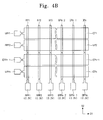
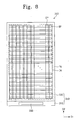
- FIG. 1 is a plan view of a display apparatus according to example embodiments.
- a display apparatus 100 may include a display panel 150 and a driving circuit 130 configured to provide a driving signal to the display panel 150.
- the display panel 150 may include a first substrate 110 and a second substrate 120 opposite the first substrate 110.
- a liquid crystal layer may be interposed between the first substrate 110 and the second substrate 120.
- the first substrate 110 may be divided into a display area DA provided with a plurality of pixels (not shown) and a non-display area PA provided with the driving circuit 130 or signal lines (not shown).
- the display area DA may be used to display an image, e.g., gradation of an image.
- the first substrate 110 ay have an area greater than the second substrate 120 so that the driving circuit 130 can be mounted on the first substrate 110.
- a plurality of gate lines, a plurality of data lines, a plurality of switching devices connected to the gate lines and the data lines, and a plurality of pixel electrodes connected to the switching devices may be provided on the first substrate 110.
- the gate lines and the data lines may extend along first and second directions D1 and D2, respectively, crossing each other.
- a configuration or structure of the first substrate 110 will be described below in more detail with reference to FIGS. 2 and 3 .
- the electrode patterns EP may extend along the first direction D1 and the barrier patterns BP may extend along the second direction D2.
- the electrode patterns EP may be arranged along the second direction D2, i.e., the electrode patterns EP may be spaced apart from each other along the second direction D2
- the barrier patterns BP may be arranged along the first direction D1, i.e., the barrier patterns BP may be spaced apart from each other along the first direction D1.
- the barrier patterns BP may be electrically isolated from the electrode patterns EP.
- the barrier patterns BP may enable a viewer to perceive a stereoscopic image.
- the barrier patterns BP may be configured to allow each eye to see a different group of the pixels, i.e., the barrier patterns BP may be configured to allow each eye to see a slightly different image. For instance, due to the presence of the barrier patterns BP, lights emitted from a first group of the pixels may be delivered to a left eye of a viewer located at a specific external position and lights emitted from a second group of the pixels, i.e., a different group of pixels, may be delivered to a right eye of the viewer, i.e., so the different images delivered to each eye, e.g., gradation image, may be perceived together as a stereoscopic image.
- lights emitted from a first group of the pixels may be delivered to a left eye of a viewer located at a specific external position and lights emitted from a second group of the pixels, i.e., a different group of pixels, may be delivered to a right eye of the viewer, i.e., so the different images delivered
- the electrode patterns EP and the barrier patterns BP may be configured to detect an external touch event on the display area DA.
- the barrier patterns BP may include a conductive material and/or a material capable of absorbing or shielding a light, e.g., the barrier patterns BP may be formed of at least one conductive material capable of absorbing or shielding a light.
- application of voltage to both the electrode patterns EP and the barrier patterns BP may facilitate detection of external touch, as will be discussed in more detail below with reference to FIGS. 4A through 7 .
- the driving circuit 130 may be disposed in a portion of the non-display area PA of the first substrate 110 not facing the second substrate 120.
- the driving circuit 130 may be directly formed on the first substrate 110 using a deposition process.
- the driving circuit 130 may be provided in a chip-on-glass manner.
- the driving circuit 130 may include a gate driver providing a gate signal to at least one of the gate lines and a data driver providing a data signal to at least one of the data lines.
- the driving circuit 130 may be configured to apply a reference voltage or sensing signals to the electrode patterns EP or to measure voltages of the barrier patterns BP.
- the display area DA may include a first pair of opposite sides parallel to the second direction D2 and a second pair of opposite sides that are parallel to the first direction D1 and are shorter than the first pair of opposite sides.
- the driving circuit 130 may be disposed in the non-display area PA adjacent to one of the short sides of the display area DA and along the first direction D1.
- This configuration of the driving circuit 130 may be applied to realize a small-size display device, e.g., a cellular phone or a smartphone, or a specific large-size display device, but example embodiments of the inventive concepts are not be limited thereto.
- the driving circuit 130 may be disposed in the non-display area adjacent to one of the long sides of the display area DA along the second direction D2.
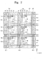
- FIG. 2 is an enlarged plan view of the display apparatus shown in FIG. 1
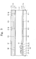
- FIG. 3 is a sectional view taken along a line I-I' of FIG. 2
- FIG. 2 shows an exemplary enlarged view of six pixel regions that correspond to a portion of the pixels described with reference to FIG. 1 .
- the display apparatus 100 may include a plurality of gate lines, e.g., first to third gate lines GL1 to GL3, which may extend along the first direction D1 and be separated from each other. Further, the display apparatus 100 may include a plurality of data lines, e.g., first to third data lines DL1 to DL3, which may extend along the second direction D2 to cross the gate lines, e.g., the first to third gate lines GL1 to GL3, and be separated from each other.
- gate lines e.g., first to third gate lines GL1 to GL3
- data lines e.g., first to third data lines DL1 to DL3
- the display apparatus 100 may include a plurality of transistors, e.g., first to sixth thin-film transistors TR1 to TR6, which may be connected to the gate lines, e.g., first to third gate lines GL1 to GL3, and to the data lines, e.g., first to third data lines DL1 to DL3, to serve as switching devices.
- first to sixth thin-film transistors TR1 to TR6 which may be connected to the gate lines, e.g., first to third gate lines GL1 to GL3, and to the data lines, e.g., first to third data lines DL1 to DL3, to serve as switching devices.
- Each of the first to sixth thin-film transistors TR1 to TR6 may be connected to a corresponding one of the first to third gate lines GL1 to GL3 and to a corresponding one of the first to third data lines DL1 to DL3.
- the first thin-film transistor TR1 may be connected to the first gate line GL1 and the first data line DL1
- the second thin-film transistor TR2 may be connected to the second gate line GL2 and the first data line DL1
- the third thin-film transistor TR3 may be connected to the third gate line GL3 and the first data line DL1
- the fourth thin-film transistor TR4 may be connected to the first gate line GL1 and the second data line DL2
- the fifth thin-film transistor TR5 may be connected to the second gate line GL2 and the second data line DL2
- the sixth thin-film transistor TR6 may be connected to the third gate line GL3 and the second data line DL2.
- Each of the first to sixth thin-film transistors TR1 to TR6 may include a gate electrode GE connected to, e.g., extending from, the corresponding gate line, a source electrode SE connected to, e.g., extending from, the corresponding data line, and a drain electrode DE separated from the source electrode SE.
- the display apparatus 100 may further include a plurality of pixels, e.g., first to sixth pixel electrodes PE1 to PE6, which may be connected to the drain electrodes DE of corresponding transistors, e.g., first to sixth thin-film transistors TR1 to TR6, through contact holes CH.
- first to sixth pixel electrodes PE1 to PE6 which may be connected to the drain electrodes DE of corresponding transistors, e.g., first to sixth thin-film transistors TR1 to TR6, through contact holes CH.
- the display apparatus 100 may further include storage lines, e.g., first to third storage lines SL1 to SL3, which may extend along the first direction D1 and be spaced apart from the gate lines, e.g., first to third gate lines GL1 to GL3.
- the display apparatus 100 may further include storage electrodes connected to, e.g., extending from, the storage lines.
- first and fourth storage electrodes ST1 and ST4 may be connected to the first storage line SL1
- second and fifth storage electrodes ST2 and ST5 may be connected to the second storage line SL2, and third and sixth storage electrodes ST3 and ST6 may be connected to the third storage line SL3.
- the first to sixth storage electrodes ST1 to ST6 may be disposed to face the first to sixth pixel electrodes PE1 to PE6, respectively, thereby forming storage capacitors.
- the display apparatus 100 may include the first substrate 110, the second substrate 120, and a liquid crystal layer LC interposed between the first and second substrates 110 and 120.
- the first substrate 110 may include a first base substrate 111, a gate electrode GE disposed on the first base substrate 111, and a first insulating layer 112 disposed on the gate electrode GE and the first base substrate 111.
- the first base substrate 111 may be formed of, e.g., a transparent glass substrate or a plastic substrate, and the first insulating layer 112 may be formed of a transparent insulating material, e.g., a silicon nitride (SiNx) layer or a silicon oxide (SiOx) layer.
- An active layer ACL and an ohmic contact layer OCL may be disposed on a portion of the first insulating layer 112 adjacent to the gate electrode GE.
- a source electrode SE and a drain electrode DE spaced apart from each other may be disposed on the ohmic contact layer OCL and the first insulating layer 112.
- the first to third data lines DL1 to DL3 may be disposed on the first insulating layer 112.
- a second insulating layer 113 may be disposed on the source electrode SE, the drain electrode DE, and the first to third data lines DL1 to DL3.
- the first to sixth pixel electrodes PE1 to PE6 may be disposed on the second insulating layer 113.
- the second insulating layer 113 may be formed to define the contact holes CH, each of which exposes at least a portion of the drain electrode DE.
- the first pixel electrode PE1 may be connected to the drain electrode DE of the first thin-film transistor TR1 through the contact hole CH.
- the second substrate 120 may include a second base substrate 121, a black matrix BM disposed on the second base substrate 121, a colour filter layer 122 disposed on the black matrix BM and the second base substrate 121.
- the colour filter layer 122 may include a red colour filter CFR realizing red colour, a green colour filter realizing green colour, and a blue colour filter realizing blue colour.
- the electrode patterns EP may be disposed on the colour filter layer 122.
- the second substrate 120 may include the barrier patterns BP, which may be disposed on the second base substrate 121 to face the electrode patterns EP.
- the barrier patterns BP and the black matrix BM may be positioned on opposite surfaces of the second base substrate 121, and may at least partially overlap.
- the second base substrate 121 may be between the barrier patterns BP and the electrode patterns EP, e.g., the colour filter layer 122, the black matrix BM, the second base substrate 121, and the barrier patterns BP may be sequentially stacked on the electrode patterns EP.
- the barrier patterns BP may overlap respective data lines and source electrodes.
- the second substrate 120 may include a polarizing film 123 disposed on the barrier patterns BP.
- the polarizing film 123 may be configured to convert light of undefined or mixed polarization into light with a predetermined, well-defined polarization (e.g., linear polarization).
- a predetermined, well-defined polarization e.g., linear polarization
- the first data line DL1, the first gate line GL1, the first thin-film transistor TR1, and the first pixel electrode PE1 may constitute a first pixel LR configured to emit a red light.
- the first data line DL1, the second gate line GL2, the second thin-film transistor TR2, and the second pixel electrode PE2 may constitute a second pixel LG configured to emit a green light.
- the first data line DL1, the third gate line GL3, the third thin-film transistor TR3, and the third pixel electrode PE3 may constitute a third pixel LB configured to emit a blue light.
- the first, second, and third pixels LR, LG, and LB may be red, green, and blue pixels, respectively.
- the second data line DL2, the first gate line GL1, the fourth thin-film transistor TR4, and the fourth pixel electrode PE4 may constitute a fourth pixel RR configured to emit a red light.
- the second data line DL2, the second gate line GL2, the fifth thin-film transistor TR5, and the fifth pixel electrode PE5 may constitute a fifth pixel RG configured to emit a green light.
- the second data line DL2, the third gate line GL3, the sixth thin-film transistor TR6, and the sixth pixel electrode PE6 may constitute a sixth pixel RB configured to emit a blue light.
- the fourth, fifth, and sixth pixels RR, RG, and RB may be red, green, and blue pixels, respectively.
- the display apparatus 100 may be configured in such a way that the first and second positions correspond to both eyes, respectively, of a viewer located at a specific position outside the display apparatus 100. This enables the viewer to perceive a stereoscopic image.
- the electrode patterns EP and the barrier patterns BP will be exemplarily described with reference to FIGS. 2-3 .
- the electrode patterns EP may be disposed to face the first to sixth pixel electrodes PE1 to PE6, and thus, an electric field can be generated therebetween.
- Each of the barrier patterns BP may be interposed between two adjacent pixels in the first direction D1, as illustrated in FIG. 2 , thereby preventing or substantially minimizing propagation of light between adjacent pixels in the first direction D1.
- two pixels of the first to sixth pixels LR, LG, LB, RR, RG, and RB which are adjacent to each other in the second direction D2 may be configured to realize two different colours.
- Two pixels of the first to sixth pixels LR, LG, LB, RR, RG, and RB, which are adjacent to each other in the first direction D1 may be configured to realize the same colour but transmit light to two different positions, i.e., two positions corresponding to respective right and left eyes. Therefore, each of the barrier patterns BP may be interposed to prevent or substantially minimize propagation of light between adjacent pixels that emit the same colour but transmit light to different positions, e.g., to different eyes.
- each of the first to sixth pixels LR, LG, LB, RR, RG, and RB may be configured in such a way that sides thereof along the first direction D1 may be longer than sides thereof along the second direction D2.
- a first directional width along the first direction D1 may be greater than a second directional width measured along the second direction D2.
- the barrier patterns BP may be disposed to extend along the second direction D2. That is, the barrier patterns BP may extend in parallel to the second directional width of the pixels.
- the electrode patterns EP may be connected to the first to third storage lines SL1 to SL3 in the non-display area PA.
- each of the first to third storage lines SL1 to SL3 may be connected to the corresponding one of the electrode patterns EP, and the same signal may be delivered to the storage line and the electrode pattern connected to each other.
- the first to third storage lines SL1 to SL3 may be disposed to be parallel to the electrode patterns EP, as shown in FIG. 2 , thereby facilitating such connections between the storage lines and the electrode patterns.
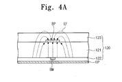
- FIGS. 4A , 4B , 5A , and 5B a method of detecting an external touch event will be described with reference to FIGS. 4A , 4B , 5A , and 5B .
- FIG. 4A is an enlarged sectional view of a portion of the second substrate 120 shown in FIG. 3
- FIG. 4B is a plan view of the barrier patterns and the electrode patterns.
- FIG. 4A shows an electric field EF generated between one of the electrode patterns EP and one of the barrier patterns BP when no external touch event occurs, i.e., when no external objects touch the second substrate 120.
- the electric field EF generated by the sensing signal may induce voltage in the barrier pattern BP.
- the electric field EF generated by the sensing signal may induce voltage of about 0.3V in the barrier pattern BP.
- the electrode patterns EP may include first to n-th electrode patterns EP1 to EPn (n is one of natural numbers) extending along the first direction D1 and arranged along the second direction D2.
- the barrier patterns BP may include first to m-th barrier pattern BP1 to BPm (m is one of natural numbers) extending along the second direction D2 and arranged along the first direction D1.
- the display apparatus 100 may include first to n-th electrode pattern pads EPP1 to EPPn connected to the first to n-th electrode pattern EP1 to EPn in the non-display area (PA in FIG. 1 ) and first to m-th barrier pattern pads BPP1 to BPPm connected to the first to m-th barrier patterns BP1 to BPm in the non-display area (PA in FIG. 1 ).
- the first to n-th electrode pattern pads EPP1 to EPPn may be used as pathways transmitting the sensing signals and the first to m-th barrier pattern pads BPP1 to BPPm may be used to detect voltages of the first to m-th barrier patterns BP1 to BPm.
- the display apparatus 100 may be configured to apply the sensing signals sequentially to the first to n-th electrode patterns EP1 to EPn and to measure voltages of the first to m-th barrier patterns BP1 to BPm synchronously with the sensing signals.
- the measurement of the voltages at the barrier patterns may determine whether an external touch event exerted on the second substrate 120 happens or not.
- the first to m-th barrier patterns BP1 to BPm may have the same voltage, i.e., the barrier pattern pads BPP1 to BPPm may measure a same voltage of about o.3V at the barrier patterns BP1 to the BPm.
- the barrier pattern pads BPP1 to BPPm may measure a same voltage of about o.3V at the barrier patterns BP1 to the BPm.
- FIG. 5A is an enlarged sectional view illustrating a portion of the second substrate 120 when an external touch event occurs
- FIG. 5B is a plan view of the barrier patterns and the electrode patterns when an external touch event occurs.
- FIG. 5A shows an electric field EF generated between one of the electrode patterns EP and one of the barrier patterns BP when an external touch event exerted on the second substrate 120 occurs.
- a sensing signal applied to the electrode pattern EP generates an electric field EF around the barrier pattern BP to induce voltage in the barrier pattern BP, as described with reference to FIG. 4A .
- the induced voltage applied to the barrier pattern BP changes, i.e., relatively to the induced voltage in the barrier pattern BP without a touch event. That is, an electric potential of the finger FG, which may be in a ground state, disturbs the electric field EF generated by the sensing signal, as shown in FIG. 5A , and thus, induces a different voltage value in the barrier pattern BP, as compared with the case of FIG.
- applying repeatedly and alternately the sensing signals of 3V and oV to the electrode pattern EP may induce a voltage of about o.2V in the barrier pattern BP.
- a voltage of about o.2 V may be measured from the second barrier pattern BP2 and the (m-1)-th barrier pattern BPm-1 in response to the sensing signals applied to the second electrode pattern EP2, and a voltage of about o.3 V may be measured from other barrier patterns with the exception of the second barrier pattern BP2 and the (m-1)-th barrier pattern BPm-1. This measurement may determine whether one or more external touch events occur at one or more positions of the second substrate 120.
- FIG. 6 is an enlarged plan view of barrier and electrode patterns according to other example embodiments of the inventive concepts.
- the electrode patterns EP may include first to n-th electrode patterns EP1 to EPn extending along the first direction D1 and arranged along the second direction D2, and the barrier patterns BP may include first to m-th barrier pattern BP1 to BPm extending along the second direction D2 and arranged along the first direction D1.
- the display apparatus 100 may include first to n-th electrode pattern pads EPP1 to EPPn connected to the first to n-th electrode patterns EP1 to EPn in the non-display area (PA in FIG. 1 ) and first to i-th barrier pattern pads BPP1 to BPPi (i is one of natural numbers) connected to a portion of the first to m-th barrier patterns BP1 to BPm in the non-display area (PA in FIG. 1 ).
- the first to n-th electrode pattern pads EPP1 to EPPn may be used as pathways transmitting the sensing signals, and the first to i-th barrier pattern pads BPP1 to BPPi may be used to measure voltages of the portion of the first to m-th barrier patterns BP1 to BPm. For instance, as shown in FIG.
- the second and (m-1)-th barrier patterns BP2 and BPm-1 may be connected to the first to i-th barrier pattern pads BPP1 to BPPi used to measure voltages of the second and (m-1)-th barrier patterns BP2 and BPm-1, while the first, third, (m-2)-th, and m-th barrier pattern BP1, BP3, and BPm-2, and BPm may not be connected to the barrier pattern pads.
- first to m-th barrier patterns BP1 to BPm may be interposed between every two substantially adjacent pixels to realize a stereoscopic image
- an external touch event exerted on the second substrate 120 may be perceived using a portion of the first to m-th barrier patterns BP1 to BPm.
- the barrier pattern pads may be merely connected to some of the barrier patterns that are used to perceive an external touch event, as shown in FIG. 6 .
- each of the first to n-th electrode patterns EP1 to EPn may have wide portions EPw1 having a first width W1 and narrow portions EPni having a second width W2 smaller than the first width W1.
- the narrow portions EPn1 may be positioned on the barrier patterns connected with the barrier pattern pad, while the remaining portions of the first to n-th electrode patterns EP1 to EPn may be the wide portions EPw1. That is, a narrow portion EPni may connect two adjacent wide portions EPw1 along the first direction D1, and may overlap a barrier pattern PB between the two adjacent wide portions EPw1.
- an electric field generated between the narrow portion EPni and the barrier pattern BP may be confined to a reduced region, as compared with the case of the wide portion. This may enable to perceive an external touch event with improved sensitivity.
- FIG. 7 is an enlarged plan view of barrier and electrode patterns according to still other example embodiments of the inventive concepts.
- the electrode patterns EP may include first to n-th electrode patterns EP1 to EPn extending along the first direction D1 and arranged along the second direction D2, and the barrier patterns BP may include first to m-th barrier pattern BP1 to BPm extending along the second direction D2 and arranged along the first direction D1.
- the display apparatus 100 may include first to n-th electrode pattern pads EPP1 to EPPn and first to j-th barrier pattern pads BPP1 to BPPj (j is one of natural numbers).
- the first to n-th electrode pattern pads EPP1 to EPPn may be connected to the first to n th electrode patterns EP1 to EPn, respectively, in the non-display area (PA in FIG. 1 ), and each of the first to j-th barrier pattern pads BPP1 to BPPj may be connected to at least two of the first to m-th barrier patterns BP1 to BPm in the non-display area (PA in FIG. 1 ).
- the first to n-th electrode pattern pads EPP1 to EPPn may be used as pathways transmitting the sensing signals, and the first to j-th barrier pattern pads BPP1 to BPPj may be used to measure voltages thereof.
- the second and third barrier patterns BP2 and BP3 may be connected in common to a first barrier pattern pad BPP1 in common, and the (m-2)-th and (m-1)-th barrier patterns BPm-2 and BPm-1 may be connected in common to aj-th barrier pattern pad BPPj, while the first and m-th barrier patterns BP1 and BPm may not be connected to the barrier pattern pads.
- each of the first to n-th electrode patterns EP1 to EPn may have wide portions EPw2 having a first width W1 and narrow portions EPn2' having a second width W2 smaller than the first width W1.
- the narrow portions EPn2' may be positioned on the barrier patterns BP connected with the barrier pattern pad BPP, while the remaining portions of the first to n-th electrode patterns EP1 to EPn may be the wide portions EPw2. It is noted that the narrow portions EPn2' in FIG.7 are longer along the first direction D1 than the narrow portions EPn2 in FIG. 6 , i.e., each narrow portion EPn2' extends to overlap two barrier patterns BP connected to a same barrier pattern pad BPP.
- FIG. 8 is a plan view of a display apparatus according to other example embodiments of the inventive concepts.
- a display apparatus 300 may include a display panel 350 and a driving circuit 330 configured to provide a driving signal to the display panel 350.
- the display panel 350 may include a first substrate 310 and a second substrate 320 opposite the first substrate 310.
- a liquid crystal layer may be interposed between the first substrate 310 and the second substrate 320.
- the first substrate 310 may be divided into a display area DA provided with a plurality of pixels (not shown) and a non-display area PA provided with the driving circuit 330 or signal lines (not shown).
- the display area DA may be used to display an image.
- the first substrate 310 may have an area greater than the second substrate 320 so that the driving circuit 330 can be mounted on the first substrate 310.
- the barrier patterns BP may extend along the first direction D1 to be arranged along the second direction D2, and the electrode patterns EP may extend along the second direction D2 to be arranged along the first direction D1.
- the barrier patterns BP may be electrically isolated from the electrode patterns EP.
- the barrier patterns BP may enable a viewer to perceive a stereoscopic image.
- the barrier patterns BP may be configured to allow each eye to see a different group of the pixels.
- lights emitted from a group of the pixels may be delivered to a left eye of a viewer located at a specific external position and lights emitted from another group of the pixels may be delivered to a right eye of the viewer.
- the electrode patterns EP and the barrier patterns BP may be configured to detect an external touch event on the display area DA.
- the barrier patterns BP may include at least one of a conductive material or a material capable of absorbing or shielding a light.
- the driving circuit 330 may be disposed in a portion of the non-display area PA of the first substrate 310 not facing the second substrate 320.
- the driving circuit 330 may be directly formed on the first substrate 310 using a deposition process.
- the driving circuit 330 may be provided in a chip-on-glass manner.
- the driving circuit 330 may include a gate driver providing a gate signal to a gate line and a data driver providing a data signal to a data line.
- the driving circuit 330 may be configured to apply a reference voltage or sensing signals to the electrode patterns EP or to measure voltages of the barrier patterns BP.
- FIG. 9 is an enlarged plan view of the display apparatus shown in FIG. 8
- FIG. 10 is a sectional view taken along a line I-I' of FIG. 9
- FIG. 9 shows an exemplary enlarged view of six pixel regions that correspond to a portion of the pixels described with reference to FIG. 8 .
- the display apparatus 300 may include first and second data lines DL1 and DL2, which may extend along the first direction D1 and be separated from each other, first to third gate lines GL1 to GL3, which may extend along the second direction D2 to cross the first and second data lines DL1 and DL2 and be separated from each other, and first to sixth thin-film transistors TR1 to TR6, which may be connected to the first and second data lines DL1 and DL2 and the first to third gate lines GL1 to GL3 to serve as switching devices.
- Each of the first to sixth thin-film transistors TR1 to TR6 may be connected to a corresponding one of the first to third gate lines GL1 to GL3 and to a corresponding one of the first and second data lines DL1 and DL2.
- the first thin-film transistor TR1 may be connected to the first gate line GL1 and the first data line DL1
- the second thin-film transistor TR2 may be connected to the second gate line GL2 and the first data line DL1
- the third thin-film transistor TR3 may be connected to the third gate line GL3 and the first data line DL1
- the fourth thin-film transistor TR4 may be connected to the first gate line GL1 and the second data line DL2
- the fifth thin-film transistor TR5 may be connected to the second gate line GL2 and the second data line DL2
- the sixth thin-film transistor TR6 may be connected to the third gate line GL3 and the second data line DL2.
- Each of the first to sixth thin-film transistors TR1 to TR6 may include
- the display apparatus 300 may further include first to sixth pixel electrodes PE1 to PE6, which may be connected to respective drain electrodes DE of the first to sixth thin-film transistors TR1 to TR6 through contact holes CH.
- the display apparatus 300 may further include first to third storage lines SL1 to SL3, which may extend along the second direction D2 and be spaced apart from the first to third gate lines GL1 to GL3.
- the display apparatus 300 may further include first and fourth storage electrodes ST1 and ST4 extending from the first storage line SL1, second and fifth storage electrodes ST2 and ST5 extending from the second storage line SL2, and third and sixth storage electrodes ST3 and ST6 extending from the third storage line SL3.
- the first to sixth storage electrodes ST1 to ST6 may be disposed to face the first to sixth pixel electrodes PE1 to PE6, respectively, thereby forming storage capacitors.
- the display apparatus 300 may include the first substrate 310, the second substrate 320, and a liquid crystal layer LC interposed between the first and second substrates 310 and 320.
- the first substrate 310 may include a first base substrate 311, a gate electrode GE disposed on the first base substrate 311, second and third gate lines GL2 and GL3, and the first to second storage line SLi to SL3.
- a first insulating layer 312 may be disposed on the gate electrode GE, the second and third gate lines GL2 and GL3, the first to second storage line SL1 to SL3, and the first base substrate 311.
- An active layer ACL and an ohmic contact layer OCL may be disposed on a portion of the first insulating layer 312 adjacent the gate electrode GE.
- a source electrode SE and a drain electrode DE spaced apart from each other may be disposed on the ohmic contact layer OCL and the first insulating layer 312.
- a second insulating layer 313 may be disposed on the source electrode SE, the drain electrode DE, and the first insulating layer 312.
- the first to sixth pixel electrodes PE1 to PE6 may be disposed on the second insulating layer 313.
- the second insulating layer 313 may be formed to define the contact holes CH, each of which exposes at least a portion of the drain electrode DE.
- the first pixel electrode PE1 may be connected to the drain electrode DE of the first thin-film transistor TR1 through the contact hole CH.
- the second substrate 320 may include a second base substrate 321, a black matrix BM disposed on the second base substrate 321, a colour filter layer 322 disposed on the black matrix BM and the second base substrate 321.
- the colour filter layer 322 may include a red colour filter CFR realizing red colour, a green colour filter CFG realizing green colour, and a blue colour filter CFB realizing blue colour.
- the electrode patterns EP may be disposed on the colour filter layer 322.
- the second substrate 320 may include the barrier patterns BP, which may be disposed on the second base substrate 321 to face the electrode patterns EP.
- the second substrate 320 may include a polarizing plate 323 disposed on the barrier patterns BP.
- the first data line DL1, the first gate line GL1, the first thin-film transistor TR1, and the first pixel electrode PE1 may constitute a first pixel RR configured to emit a red light.
- the first data line DL1, the second gate line GL2, the second thin-film transistor TR2, and the second pixel electrode PE2 may constitute a second pixel RG configured to emit a green light.
- the first data line DL1, the third gate line GL3, the third thin-film transistor TR3, and the third pixel electrode PE3 may constitute a third pixel RB configured to emit a blue light.
- the first, second, and third pixels RR, RG, and RB may be red, green, and blue pixels, respectively.
- the second data line DL2, the first gate line GL1, the fourth thin-film transistor TR4, and the fourth pixel electrode PE4 may constitute a fourth pixel LR configured to emit a red light.
- the second data line DL2, the second gate line GL2, the fifth thin-film transistor TR5, and the fifth pixel electrode PE5 may constitute a fifth pixel LG configured to emit a green light.
- the second data line DL2, the third gate line GL3, the sixth thin-film transistor TR6, and the sixth pixel electrode PE6 may constitute a sixth pixel LB configured to emit a blue light.
- the fourth, fifth, and sixth pixels LR, LG, and LB may be red, green, and blue pixels, respectively.
- the display apparatus 300 may be configured in such a way that the first and second positions correspond to both eyes, respectively, of a viewer located at a specific position outside the display apparatus 300. This enables the viewer to perceive a stereoscopic image.
- the electrode patterns EP and the barrier patterns BP will be exemplarily described with reference to FIG. 9 .
- the electrode patterns EP may be disposed to face the first to sixth pixel electrodes PE1 to PE6, and thus, an electric field can be generated therebetween.
- Each of the barrier patterns BP may be interposed between two adjacent pixels in the second direction D2 to confine propagation directions of lights emitted from the first to sixth pixels RR, RG, RB, LR, LG, and LB.
- two pixels of the first to sixth pixels RR, RG, RB, LR, LG, and LB, which are adjacent to each other in the first direction D1 may be configured to realize two different colours
- two pixels of the first to sixth pixels RR, RG, RB, LR, LG, and LB, which are adjacent to each other in the second direction D2 may be configured to realize the same colour.
- example embodiments of the inventive concepts may not be limited thereto.
- each of the first to sixth pixels RR, RG, RB, LR, LG, and LB may be configured in such a way that sides thereof parallel to the second direction D2 are longer than sides thereof parallel to the first direction D1.
- a second directional width may be greater than a first directional width measured along the second direction D2.
- the barrier patterns BP may be disposed to extend along the first direction D1. That is, the barrier patterns BP may have running directions parallel to the first direction D1.
- the electrode patterns EP may be connected to the first to third storage lines SL1 to SL3 in the non-display area PA.
- each of the first to third storage lines SL1 to SL3 may be connected to the corresponding one of the electrode patterns EP, and thus, the same signal may be delivered in common to the storage line and the electrode pattern connected to each other.
- the first to third storage lines SL1 to SL3 may be disposed to be parallel to the electrode patterns EP, as shown in FIG. 9 , and this may facilitate such connections between the storage line and the electrode pattern.
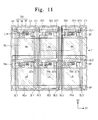
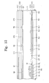
- FIG. 11 is an enlarged plan view of a display apparatus according to modifications of embodiments described with reference to FIG. 8
- FIG. 12 is a sectional view taken along a line I-I' of FIG. 11
- the display apparatus 300 may include first and second gate lines GL1 and GL2, which may extend along the first direction D1 and be separated from each other, first to third data lines DL1 to DL3, which may extend along the second direction D2 to cross the first and second gate lines GL1 and GL2 and be separated from each other, and first to sixth thin-film transistors TR1 to TR6, which may be connected to the first and second gate lines GL1 and GL2 and the first to third data lines DL1 to DL3 to serve as switching devices.
- Each of the first to sixth thin-film transistors TR1 to TR6 may be connected to a corresponding one of the first and second gate lines GL1 and GL2 and a corresponding one of the first to third data lines DL1 to DL3.
- the first thin-film transistor TR1 may be connected to the first gate line GL1 and the first data line DL1
- the second thin-film transistor TR2 may be connected to the first gate line GL1 and the second data line DL2
- the third thin-film transistor TR3 may be connected to the first gate line GL1 and the third data line DL3
- the fourth thin-film transistor TR4 may be connected to the second gate line GL2 and the first data line DL1
- the fifth thin-film transistor TR5 may be connected to the second gate line GL2 and the second data line DL2
- the sixth thin-film transistor TR6 may be connected to the second gate line GL2 and the third data line DL3.
- Each of the first to sixth thin-film transistors TR1 to TR6 may include a gate electrode GE extending from the corresponding gate line, a source electrode SE extending from the corresponding data line, and a drain electrode DE separated from the source electrode SE.
- the display apparatus 300 may further include first to sixth pixel electrodes PE1 to PE6, which may be connected to corresponding drain electrodes DE of the first to sixth thin-film transistors TR1 to TR6 through contact holes CH.
- the display apparatus 300 may further include first to third storage lines SL1 to SL3, which may extend along the second direction D2 and be spaced apart from the first to third data lines DL1 to DL3.
- the display apparatus 300 may further include first and fourth storage electrodes ST1 and ST4 extending from the first storage line SL1, second and fifth storage electrodes ST2 and ST5 extending from the second storage line SL2, and third and sixth storage electrodes ST3 and ST6 extending from the third storage line SL3.
- the first to sixth storage electrodes ST1 to ST6 may be disposed to face the first to sixth pixel electrodes PE1 to PE6, respectively, thereby forming storage capacitors.
- the display apparatus 300 may include the first substrate 310, the second substrate 320, and a liquid crystal layer LC interposed between the first and second substrates 310 and 320.
- the first substrate 310 may include the first base substrate 311, the gate electrode GE disposed on the first base substrate 311, and the first to third gate lines GL1 to GL3.
- the first insulating layer 312 may be disposed on the gate electrode GE, the first to third gate lines GL1 to GL3, and the first base substrate 311.
- the active layer ACL and the ohmic contact layer OCL may be disposed on a portion of the first insulating layer 312 to face the gate electrode GE.
- the source electrode SE and the drain electrode DE spaced apart from each other may be disposed on the ohmic contact layer OCL and the first insulating layer 312.
- the first to third data lines DL1 to DL3 and the first to third storage lines SL1 to SL3 may be disposed, spaced apart from each other, on the first insulating layer 312.
- the second insulating layer 313 may be disposed on the source electrode SE, the drain electrode DE, the first to third storage lines SL1 to SL3, and the first to third data lines DL1 to DL3.
- the second insulating layer 313 may be formed to define the contact holes CH, each of which exposes at least a portion of the drain electrode DE.
- the first pixel electrode PE1 may be connected to the drain electrode DE of the first thin-film transistor TR1 through the contact hole CH.
- the second substrate 320 may include the second base substrate 321, the black matrix BM disposed on the second base substrate 321, and the colour filter layer 322 disposed on the black matrix BM and the second base substrate 321.
- the colour filter layer 322 may include the red colour filter CFR realizing red colour, the green colour filter CFG realizing green colour, and the blue colour filter CFB realizing blue colour.
- the electrode patterns EP may be disposed on the colour filter layer 322.
- the second substrate 320 may include the barrier patterns BP, which may be disposed on the second base substrate 321 to face the electrode patterns EP, e.g., to partially overlap the electrode patterns EP.
- the second substrate 320 may include the polarizing plate 323 disposed on the barrier patterns BP.
- the first data line DL1, the first gate line GL1, the first thin-film transistor TR1, and the first pixel electrode PE1 may constitute the first pixel RR configured to emit a red light.
- the second data line DL2, the first gate line GL1, the second thin-film transistor TR2, and the second pixel electrode PE2 may constitute the second pixel RG configured to emit a green light.
- the third data line DL3, the first gate line GL1, the third thin-film transistor TR3, and the third pixel electrode PE3 may constitute the third pixel RB configured to emit a blue light.
- the first, second, and third pixels RR, RG, and RB may be red, green, and blue pixels, respectively.
- the first data line DL1, the second gate line GL2, the fourth thin-film transistor TR4, and the fourth pixel electrode PE4 may constitute the fourth pixel LR configured to emit a red light.
- the second data line DL2, the second gate line GL2, the fifth thin-film transistor TR5, and the fifth pixel electrode PE5 may constitute the fifth pixel LG configured to emit a green light.
- the third data line DL3, the second gate line GL2, the sixth thin-film transistor TR6, and the sixth pixel electrode PE6 may constitute the sixth pixel LB configured to emit a blue light.
- the fourth, fifth, and sixth pixels LR, LG, and LB may be red, green, and blue pixels, respectively.
- the display apparatus 300 may be configured in such a way that the first and second positions correspond to both eyes, respectively, of a viewer located at a specific position outside the display apparatus 300. This enables the viewer to perceive a stereoscopic image.
- the electrode patterns EP and the barrier patterns BP will be exemplarily described with reference to FIG. 11 .
- the electrode patterns EP may be disposed to face the first to sixth pixel electrodes PE1 to PE6, and thus, an electric field can be generated therebetween.
- Each of the barrier patterns BP may be interposed between two adjacent pixels in the second direction D2 to confine propagation directions of lights emitted from the first to sixth pixels RR, RG, RB, LR, LG, and LB.
- two pixels of the first to sixth pixels RR, RG, RB, LR, LG, and LB, which are adjacent to each other in the first direction D1 may be configured to realize two different colours
- two pixels of the first to sixth pixels RR, RG, RB, LR, LG, and LB, which are adjacent to each other in the second direction D2 may be configured to realize the same colour.
- example embodiments of the inventive concepts may not be limited thereto.
- each of the first to sixth pixels RR, RG, RB, LR, LG, and LB may be configured in such a way that sides thereof parallel to the second direction D2 are longer than sides thereof parallel to the first direction D1.
- a second directional width may be greater than a first directional width measured along the second direction D2.
- the barrier patterns BP may be disposed to extend along the first direction D1. That is, the barrier patterns BP may have running directions parallel to the first direction D1.
- the electrode patterns EP may be connected to the first to third storage lines SL1 to SL3 in the non-display area PA.
- each of the first to third storage lines SL1 to SL3 may be connected to the corresponding one of the electrode patterns EP, and thus, the same signal may be delivered in common to the storage line and the electrode pattern connected to each other.
- the first to third storage lines SL1 to SL3 may be disposed at the same vertical level or layer as the first to third data lines DL1 to DL3. In this case, the first to third storage lines SL1 to SL3 can be disposed to be parallel to the electrode patterns EP.
- a display apparatus may be configured to realize a stereoscopic image using barrier patterns and to detect an external touch event using the barrier patterns and electrode patterns. That is, the barrier patterns and electrode patterns according to example embodiments may be arranged within a display panel with respect to pixels, such that both touch event and realization of a spectroscopic image may be achieved. Accordingly, manufacturing and mounting of a separate touch panel on the display device may not be required. As a result, it may be possible to reduce cost and time to fabricate a display apparatus capable of both realizing a stereoscopic image and perceiving a touch event. In addition, it may be possible to reduce a thickness of the display apparatus.
- a conventional stereoscopic image display apparatus with a touch panel may include a separate touch panel that is mounted on a display panel using an additional adhesive layer.
- use of such a conventional stereoscopic image display apparatus, i.e., with a separate touch panel may lead to an increase in cost and time to fabricate the display apparatus, as well as to an increased thickness of the display apparatus.
Description
- The present invention relates generally to a display apparatus. More particularly, the invention relates to a display apparatus including barrier patterns that displays a stereoscopic image and detects an external touch.
- A display apparatus, e.g., a stereoscopic image display apparatus, with a touch panel is an electronic visual display configured to detect a touch event occurring on a display area and to receive a user's command corresponding to the touch event. The display apparatus with the touch panel does not require an additional input device, e.g., a keyboard and/or a mouse, and thus, the application thereof is continuously expanding.
- The touch panel of a display apparatus may be, e.g., a resistive sensing touch panel, an optical sensing touch panel, or a capacitive sensing touch panel. For example, the capacitive sensing touch panel may be configured to measure a change in capacitance caused by touching the surface of the touch panel.
- The stereoscopic image display apparatus refers to a display that realizes a three-dimensional, i.e., stereoscopic, image. In the stereoscopic image display apparatus, the stereoscopic image may be realized using a binocular disparity that refers to the difference in image location of an object seen by the left and right eyes. To detect a touch event and realize a stereoscopic image, a display apparatus may require a display panel for displaying a stereoscopic image and a touch panel for detecting a touch event.
-
EP 2437143 relates to a 3-dimensional flat panel display with a built-in touch screen panel. -
KR 100824539 -
EP 2184666 relates to a multi-point sensing method applicable to a capacitive touch panel to detect a voltage variation of every electrode patterned on two parallel electrode layers. -
US 2009/086150 relates to a liquid crystal display panel and a parallax barrier with a barrier light-shielding layer patterned on a barrier glass, bonded with an adhesive layer composed of an ultraviolet curing resin, provided with an area without a light-shielding layer on the peripheral portion of the parallax barrier, and a sealing material arranged between a TFT substrate and a CF substrate with at least a portion thereof overlapping with the area without the light-shielding layer. - Embodiments provide a display apparatus according to
claim 1 with barrier patterns configured to both realize a stereoscopic image and to perceive a touch event. According to example embodiments, a display apparatus may include a display panel, a plurality of electrode patterns, and a plurality of barrier patterns. - According to some example embodiments, a display apparatus may include a first substrate opposite a second substrate, a plurality of electrode patterns in the second substrate, the plurality of electrode patterns extending along a first direction, a plurality of barrier patterns in the second substrate, the plurality of barrier patterns being insulated from the electrode patterns and extending along a second direction crossing the first direction, and a plurality of pixels, the first and second substrates with the pixels defining a display panel, and each pixel including a gate line extending along a third direction, a data line extending along a fourth direction, and a pixel electrode electrically connected to the gate line and the data line, the pixel electrode being configured to generate an electric field with a corresponding electrode pattern of the plurality of electrode patterns to display an image.
- The first and third directions may be parallel to each other, and the second and fourth directions may be parallel to each other.
- Each pixel of the plurality of pixels may further include a storage line spaced apart from the gate line and parallel thereto. The storage line may be connected to a corresponding electrode pattern of the plurality of electrode patterns. Each pixel of the plurality of pixels may further include a storage electrode extending from the storage line to face at least a portion of the pixel electrode. Each pixel of the plurality of pixels may further include a colour filter overlapping the pixel electrode to realize one of red, green, and blue colours. The plurality of pixels may include at least a red pixel configured to display red colour, a green pixel configured to display green colour, and a blue pixel configured to display blue colour, the plurality of pixels being arranged to have every two pixels adjacent to each other in the second direction display different colours.
- Every two pixels adjacent to each other in the first direction may display a same colour. Each pixel of the plurality of pixels may have a first width along the first direction and a second width along the second direction, the first width being greater than the second width.
- The barrier patterns may be configured to transmit first and second images to first and second positions located outside the apparatus, respectively, the first and second images being generated from two different groups of pixels to display a stereoscopic image. The barrier patterns may include at least one conductive material capable of absorbing or shielding a light, the electrode patterns being between the first substrate and the barrier patterns.
- The apparatus may further include a driving circuit configured to provide a driving signal to the gate line, to the data line, and to the electrode patterns, the display panel further comprising a display area with the pixels and a non-display area, and the driving circuit being disposed in a portion of the non-display area adjacent to the display area in the second direction.
- The apparatus may further include a driving circuit configured to provide a driving signal to the gate line, to the data line, and to the electrode patterns, the display panel further comprising a display area with the pixels and a non-display area, and the driving circuit being disposed in a portion of the non-display area adjacent to the display area in the first direction.
- The electrode patterns and the barrier patterns may be disposed in the second substrate to face the first substrate, the electrode patterns being interposed between the first substrate and the barrier patterns.
- The apparatus may further include a liquid crystal layer interposed between the first substrate and the second substrate.
- Each pixel of the plurality of pixels may further include a switching device including a gate electrode extending from the gate line, a source electrode extending from the data line, and a drain electrode connected to the pixel electrode.
- The barrier patterns may include at least one conductive material capable of absorbing or shielding a light.
- The first and fourth directions may be parallel to each other, and the second and third directions are parallel to each other. The apparatus may further include a storage line spaced apart from the data line and parallel thereto. The storage line may be connected to a corresponding electrode pattern of the plurality of electrode patterns.
- Each pixel of the plurality of pixels may further include a colour filter facing the pixel electrode to realize one of red, green, and blue colours.
- The pixels may include at least a red pixel configured to display red colour, a green pixel configured to display green colour, and a blue pixel configured to display blue colour, the pixels being arranged to have every two adjacent pixels in the second direction display different colours.
- Every two adjacent pixels adjacent in the first direction may display the same colour.
- The first substrate may include a first base substrate, the gate line being on the first base substrate, the data and storage lines being on the first base substrate and on the gate line, the data and storage lines being electrically isolated from the gate line.
- In some embodiments, the display panel may include a first substrate, a second substrate opposite the first substrate, and a plurality of pixels, the electrode patterns may be provided in the second substrate to extend along a first direction, and the barrier patterns may be provided in the second substrate to extend along a second direction crossing the first direction. Here, the barrier patterns may be electrically insulated from the electrode patterns. Each of the pixels may include a gate line extending along the first direction, a data line extending along the second direction, and a pixel electrode electrically connected to the gate line and the data line. The pixel electrode may generate an electric field in conjunction with the corresponding one of the electrode patterns, thereby displaying a gradation of an image.
- In some other embodiments, a display apparatus may include a first substrate, a second substrate opposite the first substrate, and a plurality of pixels. The barrier patterns may be provided in the second substrate to extend along a first direction. The electrode patterns may be provided in the second substrate to extend along a second direction crossing the first direction. Here, the electrode patterns may be electrically insulated from the barrier patterns. Each of the pixels may include a gate line extending along the first direction, a data line extending along the second direction, a storage line spaced apart from the data line to extend along the second direction, and a pixel electrode electrically connected to the gate line and the data line. The pixel electrode may generate an electric field in conjunction with the corresponding one of the electrode patterns, thereby displaying a gradation of an image.
- The above and other features and advantages will become more apparent to those of ordinary skill in the art by describing in detail exemplary embodiments with reference to the attached drawings, in which:
-
FIG. 1 illustrates a schematic plan view of a display apparatus according to example embodiments; -
FIG. 2 illustrates an enlarged partial plan view of the display apparatus inFIG. 1 ; -
FIG. 3 illustrates a sectional view taken along a line I-I' ofFIG. 2 ; -
FIG. 4A illustrates an enlarged sectional view of a portion of the second substrate shown inFIG. 3 ; -
FIG. 4B illustrates an enlarged partial plan view of the barrier patterns and the electrode patterns shown inFIG. 1 ; -
FIG. 5A illustrates an enlarged sectional view of a portion of the second substrate in the presence of an external touch event; -
FIG. 5B illustrates an enlarged partial plan view of the barrier patterns and the electrode patterns in the presence of an external touch event; -
FIG. 6 illustrates a plan view of barrier and electrode patterns according to other example embodiments; -
FIG.7 illustrates a plan view of barrier and electrode patterns according to still other example embodiments; -
FIG. 8 illustrates a plan view of a display apparatus according to other example embodiments; -
FIG. 9 illustrates an enlarged partial plan view of the display apparatus inFIG. 8 ; -
FIG. 10 illustrates a sectional view taken along a line I-I' ofFIG. 9 ; -
FIG. 11 illustrates an enlarged plan view of a display apparatus according to modifications of embodiments described with reference toFIG. 8 ; and -
FIG. 12 illustrates a sectional view taken along a line I-I' ofFIG. 11 . - Spatially relative terms, such as "beneath," "below," "lower," "above," "upper" and the like, may be used herein for ease of description to describe one element's or feature's relationship to another element(s) or feature(s) as illustrated in the figures. It will be understood that the spatially relative terms are intended to encompass different orientations of the device in use or operation in addition to the orientation depicted in the figures.
- Example embodiments are described herein with reference to cross-sectional illustrations that are schematic illustrations of idealized embodiments (and intermediate structures) of example embodiments. As such, variations from the shapes of the illustrations as a result, for example, of manufacturing techniques and/or tolerances, are to be expected. Thus, example embodiments should not be construed as limited to the particular shapes of regions illustrated herein but are to include deviations in shapes that result, for example, from manufacturing. For example, an implanted region illustrated as a rectangle may have rounded or curved features and/or a gradient of implant concentration at its edges rather than a binary change from implanted to non-implanted region. Likewise, a buried region formed by implantation may result in some implantation in the region between the buried region and the surface through which the implantation takes place. Thus, the regions illustrated in the figures are schematic in nature and their shapes are not intended to illustrate the actual shape of a region of a device and are not intended to limit the scope of example embodiments.
-
FIG. 1 is a plan view of a display apparatus according to example embodiments. Referring toFIG. 1 , adisplay apparatus 100 may include adisplay panel 150 and adriving circuit 130 configured to provide a driving signal to thedisplay panel 150. Thedisplay panel 150 may include afirst substrate 110 and asecond substrate 120 opposite thefirst substrate 110. Although not depicted inFIG. 1 , a liquid crystal layer may be interposed between thefirst substrate 110 and thesecond substrate 120. - The
first substrate 110 may be divided into a display area DA provided with a plurality of pixels (not shown) and a non-display area PA provided with the drivingcircuit 130 or signal lines (not shown). The display area DA may be used to display an image, e.g., gradation of an image. As shown inFIG. 1 , thefirst substrate 110 ay have an area greater than thesecond substrate 120 so that the drivingcircuit 130 can be mounted on thefirst substrate 110. - Although not depicted in
FIG. 1 , a plurality of gate lines, a plurality of data lines, a plurality of switching devices connected to the gate lines and the data lines, and a plurality of pixel electrodes connected to the switching devices may be provided on thefirst substrate 110. Here, the gate lines and the data lines may extend along first and second directions D1 and D2, respectively, crossing each other. A configuration or structure of thefirst substrate 110 will be described below in more detail with reference toFIGS. 2 and3 . - There may be a plurality of electrode patterns EP and a plurality of barrier patterns BP in the
second substrate 120. The electrode patterns EP may extend along the first direction D1 and the barrier patterns BP may extend along the second direction D2. In other words, the electrode patterns EP may be arranged along the second direction D2, i.e., the electrode patterns EP may be spaced apart from each other along the second direction D2, and the barrier patterns BP may be arranged along the first direction D1, i.e., the barrier patterns BP may be spaced apart from each other along the first direction D1. In addition, the barrier patterns BP may be electrically isolated from the electrode patterns EP. According to example embodiments of the inventive concepts, the barrier patterns BP may enable a viewer to perceive a stereoscopic image. That is, the barrier patterns BP may be configured to allow each eye to see a different group of the pixels, i.e., the barrier patterns BP may be configured to allow each eye to see a slightly different image. For instance, due to the presence of the barrier patterns BP, lights emitted from a first group of the pixels may be delivered to a left eye of a viewer located at a specific external position and lights emitted from a second group of the pixels, i.e., a different group of pixels, may be delivered to a right eye of the viewer, i.e., so the different images delivered to each eye, e.g., gradation image, may be perceived together as a stereoscopic image. - In addition, the electrode patterns EP and the barrier patterns BP may be configured to detect an external touch event on the display area DA. For example, the barrier patterns BP may include a conductive material and/or a material capable of absorbing or shielding a light, e.g., the barrier patterns BP may be formed of at least one conductive material capable of absorbing or shielding a light. As such, application of voltage to both the electrode patterns EP and the barrier patterns BP may facilitate detection of external touch, as will be discussed in more detail below with reference to
FIGS. 4A through 7 . - The driving
circuit 130 may be disposed in a portion of the non-display area PA of thefirst substrate 110 not facing thesecond substrate 120. The drivingcircuit 130 may be directly formed on thefirst substrate 110 using a deposition process. Alternatively, the drivingcircuit 130 may be provided in a chip-on-glass manner. - The driving
circuit 130 may include a gate driver providing a gate signal to at least one of the gate lines and a data driver providing a data signal to at least one of the data lines. The drivingcircuit 130 may be configured to apply a reference voltage or sensing signals to the electrode patterns EP or to measure voltages of the barrier patterns BP. - As shown in
FIG. 1 , the display area DA may include a first pair of opposite sides parallel to the second direction D2 and a second pair of opposite sides that are parallel to the first direction D1 and are shorter than the first pair of opposite sides. In some embodiments, the drivingcircuit 130 may be disposed in the non-display area PA adjacent to one of the short sides of the display area DA and along the first direction D1. - This configuration of the driving
circuit 130 may be applied to realize a small-size display device, e.g., a cellular phone or a smartphone, or a specific large-size display device, but example embodiments of the inventive concepts are not be limited thereto. For instance, in other embodiments, the drivingcircuit 130 may be disposed in the non-display area adjacent to one of the long sides of the display area DA along the second direction D2. -
FIG. 2 is an enlarged plan view of the display apparatus shown inFIG. 1 , andFIG. 3 is a sectional view taken along a line I-I' ofFIG. 2 . In more detail,FIG. 2 shows an exemplary enlarged view of six pixel regions that correspond to a portion of the pixels described with reference toFIG. 1 . - Referring to
FIG. 2 , thedisplay apparatus 100 may include a plurality of gate lines, e.g., first to third gate lines GL1 to GL3, which may extend along the first direction D1 and be separated from each other. Further, thedisplay apparatus 100 may include a plurality of data lines, e.g., first to third data lines DL1 to DL3, which may extend along the second direction D2 to cross the gate lines, e.g., the first to third gate lines GL1 to GL3, and be separated from each other. Thedisplay apparatus 100 may include a plurality of transistors, e.g., first to sixth thin-film transistors TR1 to TR6, which may be connected to the gate lines, e.g., first to third gate lines GL1 to GL3, and to the data lines, e.g., first to third data lines DL1 to DL3, to serve as switching devices. - Each of the first to sixth thin-film transistors TR1 to TR6 may be connected to a corresponding one of the first to third gate lines GL1 to GL3 and to a corresponding one of the first to third data lines DL1 to DL3. In detail, the first thin-film transistor TR1 may be connected to the first gate line GL1 and the first data line DL1, the second thin-film transistor TR2 may be connected to the second gate line GL2 and the first data line DL1, the third thin-film transistor TR3 may be connected to the third gate line GL3 and the first data line DL1, the fourth thin-film transistor TR4 may be connected to the first gate line GL1 and the second data line DL2, the fifth thin-film transistor TR5 may be connected to the second gate line GL2 and the second data line DL2, and the sixth thin-film transistor TR6 may be connected to the third gate line GL3 and the second data line DL2. Each of the first to sixth thin-film transistors TR1 to TR6 may include a gate electrode GE connected to, e.g., extending from, the corresponding gate line, a source electrode SE connected to, e.g., extending from, the corresponding data line, and a drain electrode DE separated from the source electrode SE.
- The
display apparatus 100 may further include a plurality of pixels, e.g., first to sixth pixel electrodes PE1 to PE6, which may be connected to the drain electrodes DE of corresponding transistors, e.g., first to sixth thin-film transistors TR1 to TR6, through contact holes CH. - The
display apparatus 100 may further include storage lines, e.g., first to third storage lines SL1 to SL3, which may extend along the first direction D1 and be spaced apart from the gate lines, e.g., first to third gate lines GL1 to GL3. Thedisplay apparatus 100 may further include storage electrodes connected to, e.g., extending from, the storage lines. For example, first and fourth storage electrodes ST1 and ST4 may be connected to the first storage line SL1, second and fifth storage electrodes ST2 and ST5 may be connected to the second storage line SL2, and third and sixth storage electrodes ST3 and ST6 may be connected to the third storage line SL3. The first to sixth storage electrodes ST1 to ST6 may be disposed to face the first to sixth pixel electrodes PE1 to PE6, respectively, thereby forming storage capacitors. - Referring to
FIGS. 2-3 , thedisplay apparatus 100 may include thefirst substrate 110, thesecond substrate 120, and a liquid crystal layer LC interposed between the first andsecond substrates - The
first substrate 110 may include afirst base substrate 111, a gate electrode GE disposed on thefirst base substrate 111, and a first insulatinglayer 112 disposed on the gate electrode GE and thefirst base substrate 111. Thefirst base substrate 111 may be formed of, e.g., a transparent glass substrate or a plastic substrate, and the first insulatinglayer 112 may be formed of a transparent insulating material, e.g., a silicon nitride (SiNx) layer or a silicon oxide (SiOx) layer. - An active layer ACL and an ohmic contact layer OCL may be disposed on a portion of the first insulating
layer 112 adjacent to the gate electrode GE. A source electrode SE and a drain electrode DE spaced apart from each other may be disposed on the ohmic contact layer OCL and the first insulatinglayer 112. The first to third data lines DL1 to DL3 may be disposed on the first insulatinglayer 112. - A second insulating
layer 113 may be disposed on the source electrode SE, the drain electrode DE, and the first to third data lines DL1 to DL3. The first to sixth pixel electrodes PE1 to PE6 may be disposed on the second insulatinglayer 113. The secondinsulating layer 113 may be formed to define the contact holes CH, each of which exposes at least a portion of the drain electrode DE. The first pixel electrode PE1 may be connected to the drain electrode DE of the first thin-film transistor TR1 through the contact hole CH. - The
second substrate 120 may include asecond base substrate 121, a black matrix BM disposed on thesecond base substrate 121, acolour filter layer 122 disposed on the black matrix BM and thesecond base substrate 121. Thecolour filter layer 122 may include a red colour filter CFR realizing red colour, a green colour filter realizing green colour, and a blue colour filter realizing blue colour. The electrode patterns EP may be disposed on thecolour filter layer 122. - The
second substrate 120 may include the barrier patterns BP, which may be disposed on thesecond base substrate 121 to face the electrode patterns EP. For example, as illustrated inFIG. 3 , the barrier patterns BP and the black matrix BM may be positioned on opposite surfaces of thesecond base substrate 121, and may at least partially overlap. For example, thesecond base substrate 121 may be between the barrier patterns BP and the electrode patterns EP, e.g., thecolour filter layer 122, the black matrix BM, thesecond base substrate 121, and the barrier patterns BP may be sequentially stacked on the electrode patterns EP. For example, as illustrated inFIGS. 2-3 , the barrier patterns BP may overlap respective data lines and source electrodes. - The
second substrate 120 may include apolarizing film 123 disposed on the barrier patterns BP. Thepolarizing film 123 may be configured to convert light of undefined or mixed polarization into light with a predetermined, well-defined polarization (e.g., linear polarization). Although not depicted inFIG. 3 , there may be an alignment layer controlling orientation of the liquid crystalline molecules in the liquid crystal layer LC, on the first and fourth pixel electrode PE1 and PE4 and the electrode patterns EP. - Referring back to
FIG. 2 , the first data line DL1, the first gate line GL1, the first thin-film transistor TR1, and the first pixel electrode PE1 may constitute a first pixel LR configured to emit a red light. The first data line DL1, the second gate line GL2, the second thin-film transistor TR2, and the second pixel electrode PE2 may constitute a second pixel LG configured to emit a green light. The first data line DL1, the third gate line GL3, the third thin-film transistor TR3, and the third pixel electrode PE3 may constitute a third pixel LB configured to emit a blue light. In other words, the first, second, and third pixels LR, LG, and LB may be red, green, and blue pixels, respectively. - Similarly, the second data line DL2, the first gate line GL1, the fourth thin-film transistor TR4, and the fourth pixel electrode PE4 may constitute a fourth pixel RR configured to emit a red light. The second data line DL2, the second gate line GL2, the fifth thin-film transistor TR5, and the fifth pixel electrode PE5 may constitute a fifth pixel RG configured to emit a green light. The second data line DL2, the third gate line GL3, the sixth thin-film transistor TR6, and the sixth pixel electrode PE6 may constitute a sixth pixel RB configured to emit a blue light. In other words, the fourth, fifth, and sixth pixels RR, RG, and RB may be red, green, and blue pixels, respectively.
- Depending on positions and/or arrangements of the barrier patterns BP, lights emitted from the first to third pixels LR, LG and LB may be transmitted to a first position located outside the
display apparatus 100, and lights emitted from the fourth to sixth pixel RR, RG and RB may be transmitted to a second position located outside thedisplay apparatus 100. In detail, thedisplay apparatus 100 may be configured in such a way that the first and second positions correspond to both eyes, respectively, of a viewer located at a specific position outside thedisplay apparatus 100. This enables the viewer to perceive a stereoscopic image. - To provide better understanding of a relative arrangement between the first to sixth pixels LR, LG, LB, RR, RG and RB of the
first substrate 110 and the electrode patterns EP and the barrier patterns BP of thesecond substrate 120, the electrode patterns EP and the barrier patterns BP will be exemplarily described with reference toFIGS. 2-3 . As exemplarily shown inFIGS. 2-3 , the electrode patterns EP may be disposed to face the first to sixth pixel electrodes PE1 to PE6, and thus, an electric field can be generated therebetween. Each of the barrier patterns BP may be interposed between two adjacent pixels in the first direction D1, as illustrated inFIG. 2 , thereby preventing or substantially minimizing propagation of light between adjacent pixels in the first direction D1. - In detail, as shown in
FIG. 2 , two pixels of the first to sixth pixels LR, LG, LB, RR, RG, and RB, which are adjacent to each other in the second direction D2, may be configured to realize two different colours. Two pixels of the first to sixth pixels LR, LG, LB, RR, RG, and RB, which are adjacent to each other in the first direction D1, may be configured to realize the same colour but transmit light to two different positions, i.e., two positions corresponding to respective right and left eyes. Therefore, each of the barrier patterns BP may be interposed to prevent or substantially minimize propagation of light between adjacent pixels that emit the same colour but transmit light to different positions, e.g., to different eyes. - Furthermore, each of the first to sixth pixels LR, LG, LB, RR, RG, and RB may be configured in such a way that sides thereof along the first direction D1 may be longer than sides thereof along the second direction D2. In other words, for the first to sixth pixels LR, LG, LB, RR, RG, and RB, a first directional width along the first direction D1 may be greater than a second directional width measured along the second direction D2. In some embodiments, as shown in
FIG. 2 , the barrier patterns BP may be disposed to extend along the second direction D2. That is, the barrier patterns BP may extend in parallel to the second directional width of the pixels. - Although not depicted in the drawings, the electrode patterns EP may be connected to the first to third storage lines SL1 to SL3 in the non-display area PA. For instance, each of the first to third storage lines SL1 to SL3 may be connected to the corresponding one of the electrode patterns EP, and the same signal may be delivered to the storage line and the electrode pattern connected to each other. In some embodiments, the first to third storage lines SL1 to SL3 may be disposed to be parallel to the electrode patterns EP, as shown in
FIG. 2 , thereby facilitating such connections between the storage lines and the electrode patterns. - Hereinafter, a method of detecting an external touch event will be described with reference to
FIGS. 4A ,4B ,5A , and5B . -
FIG. 4A is an enlarged sectional view of a portion of thesecond substrate 120 shown inFIG. 3 , andFIG. 4B is a plan view of the barrier patterns and the electrode patterns. - In more detail,
FIG. 4A shows an electric field EF generated between one of the electrode patterns EP and one of the barrier patterns BP when no external touch event occurs, i.e., when no external objects touch thesecond substrate 120. - Referring to
FIG. 4A , when a sensing signal is applied to the electrode pattern EP, the electric field EF generated by the sensing signal may induce voltage in the barrier pattern BP. For instance, when no external touch event is exerted on thesecond substrate 120, applying repeatedly and alternately sensing signals of 3V and oV to the electrode pattern EP may induce voltage of about 0.3V in the barrier pattern BP. - Referring to
FIG. 4B , the electrode patterns EP may include first to n-th electrode patterns EP1 to EPn (n is one of natural numbers) extending along the first direction D1 and arranged along the second direction D2. The barrier patterns BP may include first to m-th barrier pattern BP1 to BPm (m is one of natural numbers) extending along the second direction D2 and arranged along the first direction D1. - The
display apparatus 100 may include first to n-th electrode pattern pads EPP1 to EPPn connected to the first to n-th electrode pattern EP1 to EPn in the non-display area (PA inFIG. 1 ) and first to m-th barrier pattern pads BPP1 to BPPm connected to the first to m-th barrier patterns BP1 to BPm in the non-display area (PA inFIG. 1 ). In some embodiments, the first to n-th electrode pattern pads EPP1 to EPPn may be used as pathways transmitting the sensing signals and the first to m-th barrier pattern pads BPP1 to BPPm may be used to detect voltages of the first to m-th barrier patterns BP1 to BPm. - In some embodiments, the
display apparatus 100 may be configured to apply the sensing signals sequentially to the first to n-th electrode patterns EP1 to EPn and to measure voltages of the first to m-th barrier patterns BP1 to BPm synchronously with the sensing signals. The measurement of the voltages at the barrier patterns may determine whether an external touch event exerted on thesecond substrate 120 happens or not. - In detail, as described with reference to
FIGS. 4A-4B , when no external touch event exerted on thesecond substrate 120 occurs, the first to m-th barrier patterns BP1 to BPm may have the same voltage, i.e., the barrier pattern pads BPP1 to BPPm may measure a same voltage of about o.3V at the barrier patterns BP1 to the BPm. When one of the first to m-th barrier pattern pads BPP1 to BPPm measures a voltage value not corresponding to the remaining barrier pattern pads, a determination of a touch even may occur, as will be described in detail below with reference toFIGS. 5A-5B . -
FIG. 5A is an enlarged sectional view illustrating a portion of thesecond substrate 120 when an external touch event occurs, andFIG. 5B is a plan view of the barrier patterns and the electrode patterns when an external touch event occurs. In detail,FIG. 5A shows an electric field EF generated between one of the electrode patterns EP and one of the barrier patterns BP when an external touch event exerted on thesecond substrate 120 occurs. - Referring to
FIG. 5A , a sensing signal applied to the electrode pattern EP generates an electric field EF around the barrier pattern BP to induce voltage in the barrier pattern BP, as described with reference toFIG. 4A . When a touch event occurs by an external object, e.g., when a finger FG touches thesecond substrate 120, the induced voltage applied to the barrier pattern BP changes, i.e., relatively to the induced voltage in the barrier pattern BP without a touch event. That is, an electric potential of the finger FG, which may be in a ground state, disturbs the electric field EF generated by the sensing signal, as shown inFIG. 5A , and thus, induces a different voltage value in the barrier pattern BP, as compared with the case ofFIG. 4A . For example, in the presence of a touch event on thesecond substrate 120 exerted by the finger FG, applying repeatedly and alternately the sensing signals of 3V and oV to the electrode pattern EP may induce a voltage of about o.2V in the barrier pattern BP. - Referring to
FIG. 5B , if external touch events on thesecond substrate 120 exerted by the finger FG occur at a first region A1, i.e., where the second electrode pattern EP2 intersects the second barrier pattern BP2, and at a second region A2, i.e., where the second electrode pattern EP2 intersects the (m-1)-th barrier pattern BPm-1, a voltage of about o.2 V may be measured from the second barrier pattern BP2 and the (m-1)-th barrier pattern BPm-1 in response to the sensing signals applied to the second electrode pattern EP2, and a voltage of about o.3 V may be measured from other barrier patterns with the exception of the second barrier pattern BP2 and the (m-1)-th barrier pattern BPm-1. This measurement may determine whether one or more external touch events occur at one or more positions of thesecond substrate 120. -
FIG. 6 is an enlarged plan view of barrier and electrode patterns according to other example embodiments of the inventive concepts. Referring toFIG. 6 , the electrode patterns EP may include first to n-th electrode patterns EP1 to EPn extending along the first direction D1 and arranged along the second direction D2, and the barrier patterns BP may include first to m-th barrier pattern BP1 to BPm extending along the second direction D2 and arranged along the first direction D1. - The
display apparatus 100 may include first to n-th electrode pattern pads EPP1 to EPPn connected to the first to n-th electrode patterns EP1 to EPn in the non-display area (PA inFIG. 1 ) and first to i-th barrier pattern pads BPP1 to BPPi (i is one of natural numbers) connected to a portion of the first to m-th barrier patterns BP1 to BPm in the non-display area (PA inFIG. 1 ). In some embodiments, the first to n-th electrode pattern pads EPP1 to EPPn may be used as pathways transmitting the sensing signals, and the first to i-th barrier pattern pads BPP1 to BPPi may be used to measure voltages of the portion of the first to m-th barrier patterns BP1 to BPm. For instance, as shown inFIG. 6 , the second and (m-1)-th barrier patterns BP2 and BPm-1 may be connected to the first to i-th barrier pattern pads BPP1 to BPPi used to measure voltages of the second and (m-1)-th barrier patterns BP2 and BPm-1, while the first, third, (m-2)-th, and m-th barrier pattern BP1, BP3, and BPm-2, and BPm may not be connected to the barrier pattern pads. - In some embodiments, although the first to m-th barrier patterns BP1 to BPm may be interposed between every two substantially adjacent pixels to realize a stereoscopic image, an external touch event exerted on the
second substrate 120 may be perceived using a portion of the first to m-th barrier patterns BP1 to BPm. In this sense, the barrier pattern pads may be merely connected to some of the barrier patterns that are used to perceive an external touch event, as shown inFIG. 6 . - As shown in
FIG. 6 , each of the first to n-th electrode patterns EP1 to EPn may have wide portions EPw1 having a first width W1 and narrow portions EPni having a second width W2 smaller than the first width W1. In some embodiments, the narrow portions EPn1 may be positioned on the barrier patterns connected with the barrier pattern pad, while the remaining portions of the first to n-th electrode patterns EP1 to EPn may be the wide portions EPw1. That is, a narrow portion EPni may connect two adjacent wide portions EPw1 along the first direction D1, and may overlap a barrier pattern PB between the two adjacent wide portions EPw1. - Due to the narrow portion EPni shown in
FIG. 6 , an electric field generated between the narrow portion EPni and the barrier pattern BP may be confined to a reduced region, as compared with the case of the wide portion. This may enable to perceive an external touch event with improved sensitivity. -
FIG. 7 is an enlarged plan view of barrier and electrode patterns according to still other example embodiments of the inventive concepts. Referring toFIG. 7 , the electrode patterns EP may include first to n-th electrode patterns EP1 to EPn extending along the first direction D1 and arranged along the second direction D2, and the barrier patterns BP may include first to m-th barrier pattern BP1 to BPm extending along the second direction D2 and arranged along the first direction D1. - The
display apparatus 100 may include first to n-th electrode pattern pads EPP1 to EPPn and first to j-th barrier pattern pads BPP1 to BPPj (j is one of natural numbers). The first to n-th electrode pattern pads EPP1 to EPPn may be connected to the first to n th electrode patterns EP1 to EPn, respectively, in the non-display area (PA inFIG. 1 ), and each of the first to j-th barrier pattern pads BPP1 to BPPj may be connected to at least two of the first to m-th barrier patterns BP1 to BPm in the non-display area (PA inFIG. 1 ). In some embodiments, the first to n-th electrode pattern pads EPP1 to EPPn may be used as pathways transmitting the sensing signals, and the first to j-th barrier pattern pads BPP1 to BPPj may be used to measure voltages thereof. For instance, as shown inFIG. 7 , the second and third barrier patterns BP2 and BP3 may be connected in common to a first barrier pattern pad BPP1 in common, and the (m-2)-th and (m-1)-th barrier patterns BPm-2 and BPm-1 may be connected in common to aj-th barrier pattern pad BPPj, while the first and m-th barrier patterns BP1 and BPm may not be connected to the barrier pattern pads. - As shown in
FIG. 7 , each of the first to n-th electrode patterns EP1 to EPn may have wide portions EPw2 having a first width W1 and narrow portions EPn2' having a second width W2 smaller than the first width W1. In some embodiments, the narrow portions EPn2' may be positioned on the barrier patterns BP connected with the barrier pattern pad BPP, while the remaining portions of the first to n-th electrode patterns EP1 to EPn may be the wide portions EPw2. It is noted that the narrow portions EPn2' inFIG.7 are longer along the first direction D1 than the narrow portions EPn2 inFIG. 6 , i.e., each narrow portion EPn2' extends to overlap two barrier patterns BP connected to a same barrier pattern pad BPP. -
FIG. 8 is a plan view of a display apparatus according to other example embodiments of the inventive concepts. Referring toFIG. 8 , adisplay apparatus 300 may include adisplay panel 350 and adriving circuit 330 configured to provide a driving signal to thedisplay panel 350. Thedisplay panel 350 may include afirst substrate 310 and asecond substrate 320 opposite thefirst substrate 310. Although not depicted inFIG. 8 , a liquid crystal layer may be interposed between thefirst substrate 310 and thesecond substrate 320. - The
first substrate 310 may be divided into a display area DA provided with a plurality of pixels (not shown) and a non-display area PA provided with the drivingcircuit 330 or signal lines (not shown). The display area DA may be used to display an image. As shown inFIG. 8 , thefirst substrate 310 may have an area greater than thesecond substrate 320 so that the drivingcircuit 330 can be mounted on thefirst substrate 310. - There may be a plurality of electrode patterns EP and a plurality of barrier patterns BP in the
second substrate 320. The barrier patterns BP may extend along the first direction D1 to be arranged along the second direction D2, and the electrode patterns EP may extend along the second direction D2 to be arranged along the first direction D1. In addition, the barrier patterns BP may be electrically isolated from the electrode patterns EP. According to example embodiments, the barrier patterns BP may enable a viewer to perceive a stereoscopic image. In some embodiments, the barrier patterns BP may be configured to allow each eye to see a different group of the pixels. For instance, due to the presence of the barrier patterns BP, lights emitted from a group of the pixels may be delivered to a left eye of a viewer located at a specific external position and lights emitted from another group of the pixels may be delivered to a right eye of the viewer. - In addition, the electrode patterns EP and the barrier patterns BP may be configured to detect an external touch event on the display area DA. In some embodiments, the barrier patterns BP may include at least one of a conductive material or a material capable of absorbing or shielding a light.
- The driving
circuit 330 may be disposed in a portion of the non-display area PA of thefirst substrate 310 not facing thesecond substrate 320. The drivingcircuit 330 may be directly formed on thefirst substrate 310 using a deposition process. Alternatively, the drivingcircuit 330 may be provided in a chip-on-glass manner. - Although not depicted in
FIG. 8 , the drivingcircuit 330 may include a gate driver providing a gate signal to a gate line and a data driver providing a data signal to a data line. The drivingcircuit 330 may be configured to apply a reference voltage or sensing signals to the electrode patterns EP or to measure voltages of the barrier patterns BP. -
FIG. 9 is an enlarged plan view of the display apparatus shown inFIG. 8 , andFIG. 10 is a sectional view taken along a line I-I' ofFIG. 9 . In more detail,FIG. 9 shows an exemplary enlarged view of six pixel regions that correspond to a portion of the pixels described with reference toFIG. 8 . - Referring to
FIG. 9 , thedisplay apparatus 300 may include first and second data lines DL1 and DL2, which may extend along the first direction D1 and be separated from each other, first to third gate lines GL1 to GL3, which may extend along the second direction D2 to cross the first and second data lines DL1 and DL2 and be separated from each other, and first to sixth thin-film transistors TR1 to TR6, which may be connected to the first and second data lines DL1 and DL2 and the first to third gate lines GL1 to GL3 to serve as switching devices. - Each of the first to sixth thin-film transistors TR1 to TR6 may be connected to a corresponding one of the first to third gate lines GL1 to GL3 and to a corresponding one of the first and second data lines DL1 and DL2. In more detail, the first thin-film transistor TR1 may be connected to the first gate line GL1 and the first data line DL1, the second thin-film transistor TR2 may be connected to the second gate line GL2 and the first data line DL1, the third thin-film transistor TR3 may be connected to the third gate line GL3 and the first data line DL1, the fourth thin-film transistor TR4 may be connected to the first gate line GL1 and the second data line DL2, the fifth thin-film transistor TR5 may be connected to the second gate line GL2 and the second data line DL2, and the sixth thin-film transistor TR6 may be connected to the third gate line GL3 and the second data line DL2. Each of the first to sixth thin-film transistors TR1 to TR6 may include a gate electrode GE extending from a corresponding gate line, a source electrode SE extending from a corresponding data line, and a drain electrode DE separated from the source electrode SE.
- The
display apparatus 300 may further include first to sixth pixel electrodes PE1 to PE6, which may be connected to respective drain electrodes DE of the first to sixth thin-film transistors TR1 to TR6 through contact holes CH. - The
display apparatus 300 may further include first to third storage lines SL1 to SL3, which may extend along the second direction D2 and be spaced apart from the first to third gate lines GL1 to GL3. Thedisplay apparatus 300 may further include first and fourth storage electrodes ST1 and ST4 extending from the first storage line SL1, second and fifth storage electrodes ST2 and ST5 extending from the second storage line SL2, and third and sixth storage electrodes ST3 and ST6 extending from the third storage line SL3. The first to sixth storage electrodes ST1 to ST6 may be disposed to face the first to sixth pixel electrodes PE1 to PE6, respectively, thereby forming storage capacitors. - Referring to
FIGS. 9 and10 , thedisplay apparatus 300 may include thefirst substrate 310, thesecond substrate 320, and a liquid crystal layer LC interposed between the first andsecond substrates - The
first substrate 310 may include afirst base substrate 311, a gate electrode GE disposed on thefirst base substrate 311, second and third gate lines GL2 and GL3, and the first to second storage line SLi to SL3. In addition, a first insulatinglayer 312 may be disposed on the gate electrode GE, the second and third gate lines GL2 and GL3, the first to second storage line SL1 to SL3, and thefirst base substrate 311. - An active layer ACL and an ohmic contact layer OCL may be disposed on a portion of the first insulating
layer 312 adjacent the gate electrode GE. A source electrode SE and a drain electrode DE spaced apart from each other may be disposed on the ohmic contact layer OCL and the first insulatinglayer 312. - A second insulating
layer 313 may be disposed on the source electrode SE, the drain electrode DE, and the first insulatinglayer 312. The first to sixth pixel electrodes PE1 to PE6 may be disposed on the second insulatinglayer 313. The secondinsulating layer 313 may be formed to define the contact holes CH, each of which exposes at least a portion of the drain electrode DE. The first pixel electrode PE1 may be connected to the drain electrode DE of the first thin-film transistor TR1 through the contact hole CH. - The
second substrate 320 may include asecond base substrate 321, a black matrix BM disposed on thesecond base substrate 321, acolour filter layer 322 disposed on the black matrix BM and thesecond base substrate 321. - The
colour filter layer 322 may include a red colour filter CFR realizing red colour, a green colour filter CFG realizing green colour, and a blue colour filter CFB realizing blue colour. The electrode patterns EP may be disposed on thecolour filter layer 322. - The
second substrate 320 may include the barrier patterns BP, which may be disposed on thesecond base substrate 321 to face the electrode patterns EP. Thesecond substrate 320 may include apolarizing plate 323 disposed on the barrier patterns BP. - Referring back to
FIG. 9 , the first data line DL1, the first gate line GL1, the first thin-film transistor TR1, and the first pixel electrode PE1 may constitute a first pixel RR configured to emit a red light. The first data line DL1, the second gate line GL2, the second thin-film transistor TR2, and the second pixel electrode PE2 may constitute a second pixel RG configured to emit a green light. The first data line DL1, the third gate line GL3, the third thin-film transistor TR3, and the third pixel electrode PE3 may constitute a third pixel RB configured to emit a blue light. In other words, the first, second, and third pixels RR, RG, and RB may be red, green, and blue pixels, respectively. - Similarly, the second data line DL2, the first gate line GL1, the fourth thin-film transistor TR4, and the fourth pixel electrode PE4 may constitute a fourth pixel LR configured to emit a red light. The second data line DL2, the second gate line GL2, the fifth thin-film transistor TR5, and the fifth pixel electrode PE5 may constitute a fifth pixel LG configured to emit a green light. The second data line DL2, the third gate line GL3, the sixth thin-film transistor TR6, and the sixth pixel electrode PE6 may constitute a sixth pixel LB configured to emit a blue light. In other words, the fourth, fifth, and sixth pixels LR, LG, and LB may be red, green, and blue pixels, respectively.
- Depending on positions and/or arrangements of the barrier patterns BP, lights emitted from the first to third pixels RR, RG, and RB may be transmitted to a first position located outside the
display apparatus 300, and lights emitted from the fourth to sixth pixel LR, LG, and LB may be transmitted to a second position located outside thedisplay apparatus 300. In more detail, thedisplay apparatus 300 may be configured in such a way that the first and second positions correspond to both eyes, respectively, of a viewer located at a specific position outside thedisplay apparatus 300. This enables the viewer to perceive a stereoscopic image. - To provide better understanding of a relative arrangement between the first to sixth pixels RR, RG, RB, LR, LG, and LB of the
first substrate 310 and the electrode patterns EP and the barrier patterns BP of thesecond substrate 320, the electrode patterns EP and the barrier patterns BP will be exemplarily described with reference toFIG. 9 . As exemplarily shown inFIG. 9 , the electrode patterns EP may be disposed to face the first to sixth pixel electrodes PE1 to PE6, and thus, an electric field can be generated therebetween. Each of the barrier patterns BP may be interposed between two adjacent pixels in the second direction D2 to confine propagation directions of lights emitted from the first to sixth pixels RR, RG, RB, LR, LG, and LB. - In some embodiments, as shown in
FIG. 9 , two pixels of the first to sixth pixels RR, RG, RB, LR, LG, and LB, which are adjacent to each other in the first direction D1, may be configured to realize two different colours, while two pixels of the first to sixth pixels RR, RG, RB, LR, LG, and LB, which are adjacent to each other in the second direction D2, may be configured to realize the same colour. But example embodiments of the inventive concepts may not be limited thereto. - Furthermore, each of the first to sixth pixels RR, RG, RB, LR, LG, and LB may be configured in such a way that sides thereof parallel to the second direction D2 are longer than sides thereof parallel to the first direction D1. In other words, for the first to sixth pixels RR, RG, RB, LR, LG, and LB, a second directional width may be greater than a first directional width measured along the second direction D2. In some embodiments, as shown in
FIG. 9 , the barrier patterns BP may be disposed to extend along the first direction D1. That is, the barrier patterns BP may have running directions parallel to the first direction D1. - Although not depicted in the drawings, the electrode patterns EP may be connected to the first to third storage lines SL1 to SL3 in the non-display area PA. For instance, each of the first to third storage lines SL1 to SL3 may be connected to the corresponding one of the electrode patterns EP, and thus, the same signal may be delivered in common to the storage line and the electrode pattern connected to each other. In some embodiments, the first to third storage lines SL1 to SL3 may be disposed to be parallel to the electrode patterns EP, as shown in
FIG. 9 , and this may facilitate such connections between the storage line and the electrode pattern. -
FIG. 11 is an enlarged plan view of a display apparatus according to modifications of embodiments described with reference toFIG. 8 , andFIG. 12 is a sectional view taken along a line I-I' ofFIG. 11 - Referring to
FIG. 11 , thedisplay apparatus 300 may include first and second gate lines GL1 and GL2, which may extend along the first direction D1 and be separated from each other, first to third data lines DL1 to DL3, which may extend along the second direction D2 to cross the first and second gate lines GL1 and GL2 and be separated from each other, and first to sixth thin-film transistors TR1 to TR6, which may be connected to the first and second gate lines GL1 and GL2 and the first to third data lines DL1 to DL3 to serve as switching devices. - Each of the first to sixth thin-film transistors TR1 to TR6 may be connected to a corresponding one of the first and second gate lines GL1 and GL2 and a corresponding one of the first to third data lines DL1 to DL3. In more detail, the first thin-film transistor TR1 may be connected to the first gate line GL1 and the first data line DL1, the second thin-film transistor TR2 may be connected to the first gate line GL1 and the second data line DL2, the third thin-film transistor TR3 may be connected to the first gate line GL1 and the third data line DL3, the fourth thin-film transistor TR4 may be connected to the second gate line GL2 and the first data line DL1, the fifth thin-film transistor TR5 may be connected to the second gate line GL2 and the second data line DL2, and the sixth thin-film transistor TR6 may be connected to the second gate line GL2 and the third data line DL3. Each of the first to sixth thin-film transistors TR1 to TR6 may include a gate electrode GE extending from the corresponding gate line, a source electrode SE extending from the corresponding data line, and a drain electrode DE separated from the source electrode SE. The
display apparatus 300 may further include first to sixth pixel electrodes PE1 to PE6, which may be connected to corresponding drain electrodes DE of the first to sixth thin-film transistors TR1 to TR6 through contact holes CH. - The
display apparatus 300 may further include first to third storage lines SL1 to SL3, which may extend along the second direction D2 and be spaced apart from the first to third data lines DL1 to DL3. Thedisplay apparatus 300 may further include first and fourth storage electrodes ST1 and ST4 extending from the first storage line SL1, second and fifth storage electrodes ST2 and ST5 extending from the second storage line SL2, and third and sixth storage electrodes ST3 and ST6 extending from the third storage line SL3. The first to sixth storage electrodes ST1 to ST6 may be disposed to face the first to sixth pixel electrodes PE1 to PE6, respectively, thereby forming storage capacitors. - Referring to
FIGS. 11 and12 , thedisplay apparatus 300 may include thefirst substrate 310, thesecond substrate 320, and a liquid crystal layer LC interposed between the first andsecond substrates - The
first substrate 310 may include thefirst base substrate 311, the gate electrode GE disposed on thefirst base substrate 311, and the first to third gate lines GL1 to GL3. In addition, the first insulatinglayer 312 may be disposed on the gate electrode GE, the first to third gate lines GL1 to GL3, and thefirst base substrate 311. - The active layer ACL and the ohmic contact layer OCL may be disposed on a portion of the first insulating
layer 312 to face the gate electrode GE. The source electrode SE and the drain electrode DE spaced apart from each other may be disposed on the ohmic contact layer OCL and the first insulatinglayer 312. In addition, the first to third data lines DL1 to DL3 and the first to third storage lines SL1 to SL3 may be disposed, spaced apart from each other, on the first insulatinglayer 312. - The second
insulating layer 313 may be disposed on the source electrode SE, the drain electrode DE, the first to third storage lines SL1 to SL3, and the first to third data lines DL1 to DL3. The secondinsulating layer 313 may be formed to define the contact holes CH, each of which exposes at least a portion of the drain electrode DE. The first pixel electrode PE1 may be connected to the drain electrode DE of the first thin-film transistor TR1 through the contact hole CH. - The
second substrate 320 may include thesecond base substrate 321, the black matrix BM disposed on thesecond base substrate 321, and thecolour filter layer 322 disposed on the black matrix BM and thesecond base substrate 321. Thecolour filter layer 322 may include the red colour filter CFR realizing red colour, the green colour filter CFG realizing green colour, and the blue colour filter CFB realizing blue colour. The electrode patterns EP may be disposed on thecolour filter layer 322. - The
second substrate 320 may include the barrier patterns BP, which may be disposed on thesecond base substrate 321 to face the electrode patterns EP, e.g., to partially overlap the electrode patterns EP. Thesecond substrate 320 may include thepolarizing plate 323 disposed on the barrier patterns BP. - Referring back to
FIG. 11 , the first data line DL1, the first gate line GL1, the first thin-film transistor TR1, and the first pixel electrode PE1 may constitute the first pixel RR configured to emit a red light. The second data line DL2, the first gate line GL1, the second thin-film transistor TR2, and the second pixel electrode PE2 may constitute the second pixel RG configured to emit a green light. The third data line DL3, the first gate line GL1, the third thin-film transistor TR3, and the third pixel electrode PE3 may constitute the third pixel RB configured to emit a blue light. In other words, the first, second, and third pixels RR, RG, and RB may be red, green, and blue pixels, respectively. - Similarly, the first data line DL1, the second gate line GL2, the fourth thin-film transistor TR4, and the fourth pixel electrode PE4 may constitute the fourth pixel LR configured to emit a red light. The second data line DL2, the second gate line GL2, the fifth thin-film transistor TR5, and the fifth pixel electrode PE5 may constitute the fifth pixel LG configured to emit a green light. The third data line DL3, the second gate line GL2, the sixth thin-film transistor TR6, and the sixth pixel electrode PE6 may constitute the sixth pixel LB configured to emit a blue light. In other words, the fourth, fifth, and sixth pixels LR, LG, and LB may be red, green, and blue pixels, respectively.
- Depending on positions and/or arrangements of the barrier patterns BP, lights emitted from the first to third pixels RR, RG and RB may be transmitted to a first position located outside the
display apparatus 300, and lights emitted from the fourth to sixth pixel LR, LG and LB may be transmitted to a second position located outside thedisplay apparatus 300. In more detail, thedisplay apparatus 300 may be configured in such a way that the first and second positions correspond to both eyes, respectively, of a viewer located at a specific position outside thedisplay apparatus 300. This enables the viewer to perceive a stereoscopic image. - To provide better understanding of a relative arrangement between the first to sixth pixels RR, RG, RB, LR, LG, and LB of the
first substrate 310 and the electrode patterns EP and the barrier patterns BP of thesecond substrate 320, the electrode patterns EP and the barrier patterns BP will be exemplarily described with reference toFIG. 11 . As exemplarily shown inFIG. 11 , the electrode patterns EP may be disposed to face the first to sixth pixel electrodes PE1 to PE6, and thus, an electric field can be generated therebetween. Each of the barrier patterns BP may be interposed between two adjacent pixels in the second direction D2 to confine propagation directions of lights emitted from the first to sixth pixels RR, RG, RB, LR, LG, and LB. - In some embodiments, as shown in
FIG. 11 , two pixels of the first to sixth pixels RR, RG, RB, LR, LG, and LB, which are adjacent to each other in the first direction D1, may be configured to realize two different colours, while two pixels of the first to sixth pixels RR, RG, RB, LR, LG, and LB, which are adjacent to each other in the second direction D2, may be configured to realize the same colour. But example embodiments of the inventive concepts may not be limited thereto. - Furthermore, each of the first to sixth pixels RR, RG, RB, LR, LG, and LB may be configured in such a way that sides thereof parallel to the second direction D2 are longer than sides thereof parallel to the first direction D1. In other words, for the first to sixth pixels RR, RG, RB, LR, LG, and LB, a second directional width may be greater than a first directional width measured along the second direction D2. In some embodiments, as shown in
FIG. 11 , the barrier patterns BP may be disposed to extend along the first direction D1. That is, the barrier patterns BP may have running directions parallel to the first direction D1. - Although not depicted in the drawings, the electrode patterns EP may be connected to the first to third storage lines SL1 to SL3 in the non-display area PA. For instance, each of the first to third storage lines SL1 to SL3 may be connected to the corresponding one of the electrode patterns EP, and thus, the same signal may be delivered in common to the storage line and the electrode pattern connected to each other. In some embodiments, as shown in
FIG. 12 , the first to third storage lines SL1 to SL3 may be disposed at the same vertical level or layer as the first to third data lines DL1 to DL3. In this case, the first to third storage lines SL1 to SL3 can be disposed to be parallel to the electrode patterns EP. - According to example embodiments of the inventive concepts, a display apparatus may be configured to realize a stereoscopic image using barrier patterns and to detect an external touch event using the barrier patterns and electrode patterns. That is, the barrier patterns and electrode patterns according to example embodiments may be arranged within a display panel with respect to pixels, such that both touch event and realization of a spectroscopic image may be achieved. Accordingly, manufacturing and mounting of a separate touch panel on the display device may not be required. As a result, it may be possible to reduce cost and time to fabricate a display apparatus capable of both realizing a stereoscopic image and perceiving a touch event. In addition, it may be possible to reduce a thickness of the display apparatus.
- In contrast, a conventional stereoscopic image display apparatus with a touch panel may include a separate touch panel that is mounted on a display panel using an additional adhesive layer. However, use of such a conventional stereoscopic image display apparatus, i.e., with a separate touch panel, may lead to an increase in cost and time to fabricate the display apparatus, as well as to an increased thickness of the display apparatus.
- Example embodiments have been disclosed herein, and although specific terms are employed, they are used and are to be interpreted in a generic and descriptive sense only and not for purpose of limitation. Accordingly, it will be understood by those of skill in the art that various changes in form and details may be made without departing from the scope of the present invention as set forth in the following claims.
Claims (15)
- A stereoscopic image display apparatus (100) having a touch sensing capability, comprising:a first substrate (110, 310) opposite a second substrate (120, 320);a plurality of electrode patterns (EP) in the second substrate, each of the electrode patterns extending along a first direction;a plurality of electrically conductive barrier patterns (BP) in the second substrate, the plurality of barrier patterns being insulated from the electrode patterns and each of the barrier patterns extending along a second direction crossing the first direction; anda plurality of pixels, the first and second substrates with the pixels defining a display panel (150, 350), and each pixel including:a gate line (GL1 - GL3) extending along a third direction,a data line (DL1 - DL3) extending along a fourth direction, anda pixel electrode (PE1 - PE6) electrically connected to the gate line and the data line,the pixel electrodes of the plurality of pixels being configured to generate an electric field with facing electrode patterns of the plurality of electrode patterns while displaying an image,wherein the barrier patterns are configured to allow each eye of a viewer located at the second substrate side to see a different group of pixels,and wherein an electric field is arranged to be applied between the electrode patterns and the barrier patterns, wherein disturbance of the electric field resulting from an external touch is used for the detection of the external touch;wherein each pixel of the plurality of pixels further comprises a storage line (SL1 - SL3) spaced apart from the gate line or the data line and parallel thereto.
- The apparatus as claimed in claim 1, wherein the first and third directions are parallel to each other, and the second and fourth directions are parallel to each other.
- The apparatus as claimed in claim 2, wherein the storage line 9 (SL1 - SL3) are each connected to a corresponding electrode pattern (EP) of the plurality of electrode patterns.
- The apparatus as claimed in claim 3, wherein each pixel of the plurality of pixels further comprises a storage electrode extending from the storage line to face at least a portion of the pixel electrode (PE1 - PE6).
- The apparatus as claimed in any one of the preceding claims, wherein each pixel of the plurality of pixels further comprises a colour filter (122, 322) overlapping the pixel electrode to realize one of red, green, and blue colours.
- The apparatus as claimed in any one of the preceding claims, wherein each pixel of the plurality of pixels has a first width along the first direction and a second width along the second direction, the first width being greater than the second width.
- The apparatus as claimed in any one of the preceding claims, wherein the barrier patterns (BP) are configured to transmit first and second images to first and second positions located outside the apparatus, respectively, the first and second images being generated from two different groups of pixels to display a stereoscopic image.
- The apparatus as claimed in any one of the preceding claims, wherein the barrier patterns (BP) include at least one conductive material capable of absorbing or shielding light, the electrode patterns being between the first substrate (110, 310) and the barrier patterns.
- The apparatus as claimed in any one of the preceding claims, further comprising a driving circuit (130, 330) configured to provide a driving signal to the gate line, to the data line, and to the electrode patterns, the display panel further comprising a display area with the pixels and a non-display area, and the driving circuit being disposed in a portion of the non-display area adjacent to the display area in the first direction or the second direction.
- The apparatus as claimed in any one of the preceding claims, wherein the electrode patterns and the barrier patterns (BP) are disposed in the second substrate to face the first substrate, the electrode patterns (EP) being interposed between the first substrate and the barrier patterns.
- The apparatus as claimed in any one of the preceding claims, wherein each pixel of the plurality of pixels further comprises a switching device (TR1 - TR6) including a gate electrode extending from the gate line, a source electrode extending from the data line, and a drain electrode connected to the pixel electrode.
- The apparatus as claimed in claim 1, wherein the first and fourth directions are parallel to each other, and the second and third directions are parallel to each other.
- The apparatus as claimed in claim 12, wherein the storage line (SL1 - SL3) may be connected to a corresponding electrode pattern (EP) of the plurality of electrode patterns.
- The apparatus as claimed in claims 12 or 13, wherein each pixel of the plurality of pixels further comprises a colour filter (122, 322) facing the pixel electrode to realize one of red, green, and blue colours.
- The apparatus as claimed in any one of the preceding claims, wherein the pixels include at least a red pixel configured to display a red colour, a green pixel configured to display a green colour, and a blue pixel configured to display a blue colour, the pixels being arranged to have every two adjacent pixels in the second direction display different colours, wherein every two adjacent pixels in the first direction may display the same colour.
Applications Claiming Priority (1)
| Application Number | Priority Date | Filing Date | Title |
|---|---|---|---|
| KR1020110046790A KR101292249B1 (en) | 2011-05-18 | 2011-05-18 | Display apparatus |
Publications (2)
| Publication Number | Publication Date |
|---|---|
| EP2525248A1 EP2525248A1 (en) | 2012-11-21 |
| EP2525248B1 true EP2525248B1 (en) | 2015-03-04 |
Family
ID=46149153
Family Applications (1)
| Application Number | Title | Priority Date | Filing Date |
|---|---|---|---|
| EP12162643.6A Active EP2525248B1 (en) | 2011-05-18 | 2012-03-30 | Autostereoscopic touch-sensing display apparatus |
Country Status (6)
| Country | Link |
|---|---|
| US (1) | US8766891B2 (en) |
| EP (1) | EP2525248B1 (en) |
| JP (1) | JP5875822B2 (en) |
| KR (1) | KR101292249B1 (en) |
| CN (2) | CN102789098B (en) |
| TW (1) | TWI470275B (en) |
Families Citing this family (8)
| Publication number | Priority date | Publication date | Assignee | Title |
|---|---|---|---|---|
| KR101292249B1 (en) | 2011-05-18 | 2013-08-02 | 삼성디스플레이 주식회사 | Display apparatus |
| TWI554916B (en) * | 2014-07-21 | 2016-10-21 | 晨星半導體股份有限公司 | Touch display panel |
| KR102230549B1 (en) | 2014-09-12 | 2021-03-22 | 삼성디스플레이 주식회사 | Touch sensible optical system and display device including the same |
| TWI560503B (en) * | 2015-01-30 | 2016-12-01 | Innolux Corp | Display panel |
| KR102382042B1 (en) | 2016-06-21 | 2022-04-04 | 삼성디스플레이 주식회사 | Touch sensing unit and electronic device having the same |
| KR102554095B1 (en) * | 2016-09-30 | 2023-07-10 | 엘지디스플레이 주식회사 | In-cell touch liquid crystal display device and method for fabricating the same |
| TWI657699B (en) * | 2017-05-12 | 2019-04-21 | 友達光電股份有限公司 | Display panel |
| US10424602B2 (en) * | 2017-05-12 | 2019-09-24 | Au Optronics Corporation | Display panel |
Family Cites Families (22)
| Publication number | Priority date | Publication date | Assignee | Title |
|---|---|---|---|---|
| JP2653014B2 (en) * | 1993-07-26 | 1997-09-10 | 日本電気株式会社 | Active matrix liquid crystal display device |
| KR20050016406A (en) | 2002-07-29 | 2005-02-21 | 샤프 가부시키가이샤 | Substrate with parallax barrier layer, method for producing substrate with parallax barrier layer, and three-dimensional display |
| KR20070044479A (en) * | 2002-07-29 | 2007-04-27 | 샤프 가부시키가이샤 | Method for producing substrate with parallax barrier layer |
| JP4572095B2 (en) * | 2004-07-15 | 2010-10-27 | Nec液晶テクノロジー株式会社 | Liquid crystal display device, portable device, and driving method of liquid crystal display device |
| KR101142996B1 (en) * | 2004-12-31 | 2012-05-08 | 재단법인서울대학교산학협력재단 | Display device and driving method thereof |
| JP4588761B2 (en) | 2005-07-11 | 2010-12-01 | シャープ株式会社 | Display device |
| KR100739067B1 (en) | 2005-11-30 | 2007-07-12 | 삼성에스디아이 주식회사 | Three-dimensional display device |
| KR100824539B1 (en) | 2007-01-02 | 2008-04-24 | 삼성에스디아이 주식회사 | Display device for stereoscopic 3d display and touch panel |
| KR101357163B1 (en) * | 2007-08-14 | 2014-02-05 | 삼성전자주식회사 | Auto stereoscopic display improving brightness |
| KR100908724B1 (en) * | 2007-10-22 | 2009-07-22 | 삼성모바일디스플레이주식회사 | Barrier device and electronic imaging device including the same |
| WO2009069358A1 (en) * | 2007-11-29 | 2009-06-04 | Sharp Kabushiki Kaisha | Display device |
| JP5246746B2 (en) * | 2008-01-21 | 2013-07-24 | 株式会社ジャパンディスプレイウェスト | Electro-optical device, method of manufacturing electro-optical device, and electronic apparatus |
| JP5153015B2 (en) | 2008-07-02 | 2013-02-27 | シャープ株式会社 | Surface-emitting display device |
| JP2010032768A (en) * | 2008-07-29 | 2010-02-12 | Hitachi Displays Ltd | Image display and manufacturing method thereof |
| TW201019194A (en) | 2008-11-07 | 2010-05-16 | Univ Nat Chiao Tung | Multi-sensing method of capacitive touch panel |
| KR101015846B1 (en) | 2009-01-16 | 2011-02-23 | 삼성모바일디스플레이주식회사 | Electronic display device |
| JP5203293B2 (en) * | 2009-05-21 | 2013-06-05 | 株式会社ジャパンディスプレイウェスト | Display device and electronic device |
| JP5333050B2 (en) * | 2009-08-25 | 2013-11-06 | ソニー株式会社 | 3D image display device and 3D image display device manufacturing method |
| CN101996535A (en) * | 2009-08-25 | 2011-03-30 | 精工爱普生株式会社 | Electro-optical device and electronic apparatus |
| KR101188983B1 (en) * | 2010-09-30 | 2012-10-08 | 삼성디스플레이 주식회사 | 3 Dimension Plat Panel Display having a Touch Screen Panel |
| KR101778229B1 (en) * | 2010-10-29 | 2017-09-14 | 삼성디스플레이 주식회사 | Organic light emitting display device |
| KR101292249B1 (en) | 2011-05-18 | 2013-08-02 | 삼성디스플레이 주식회사 | Display apparatus |
-
2011
- 2011-05-18 KR KR1020110046790A patent/KR101292249B1/en active IP Right Grant
- 2011-09-21 US US13/137,892 patent/US8766891B2/en active Active
- 2011-10-03 JP JP2011219444A patent/JP5875822B2/en active Active
-
2012
- 2012-03-03 TW TW101107243A patent/TWI470275B/en active
- 2012-03-30 EP EP12162643.6A patent/EP2525248B1/en active Active
- 2012-05-17 CN CN201210153638.XA patent/CN102789098B/en active Active
- 2012-05-17 CN CN2012202221683U patent/CN202693960U/en not_active Expired - Fee Related
Also Published As
| Publication number | Publication date |
|---|---|
| US20120293490A1 (en) | 2012-11-22 |
| KR101292249B1 (en) | 2013-08-02 |
| EP2525248A1 (en) | 2012-11-21 |
| KR20120128874A (en) | 2012-11-28 |
| JP2012242817A (en) | 2012-12-10 |
| TW201248200A (en) | 2012-12-01 |
| CN102789098B (en) | 2015-10-28 |
| CN102789098A (en) | 2012-11-21 |
| TWI470275B (en) | 2015-01-21 |
| CN202693960U (en) | 2013-01-23 |
| JP5875822B2 (en) | 2016-03-02 |
| US8766891B2 (en) | 2014-07-01 |
Similar Documents
| Publication | Publication Date | Title |
|---|---|---|
| US10459571B2 (en) | 3-dimensional flat panel display with built-in touch screen panel | |
| US11599214B2 (en) | Display device and method of manufacturing same | |
| EP2525248B1 (en) | Autostereoscopic touch-sensing display apparatus | |
| US9898121B2 (en) | Integrated capacitive sensing and displaying | |
| US8643796B2 (en) | Liquid crystal display device | |
| US9075469B2 (en) | Stereoscopic liquid crystal display device having touch panel and method for manufacturing the same | |
| CN105425403B (en) | Display device | |
| US10564747B2 (en) | Display device and sensor device | |
| CN103392198B (en) | Electrode base board and possess display device and the touch panel of this electrode base board | |
| JP5555142B2 (en) | Display device | |
| WO2018212034A1 (en) | Display device with position input function | |
| US10146378B2 (en) | Touch sensible optical system and display device including the same |
Legal Events
| Date | Code | Title | Description |
|---|---|---|---|
| PUAI | Public reference made under article 153(3) epc to a published international application that has entered the european phase |
Free format text: ORIGINAL CODE: 0009012 |
|
| AK | Designated contracting states |
Kind code of ref document: A1 Designated state(s): AL AT BE BG CH CY CZ DE DK EE ES FI FR GB GR HR HU IE IS IT LI LT LU LV MC MK MT NL NO PL PT RO RS SE SI SK SM TR |
|
| AX | Request for extension of the european patent |
Extension state: BA ME |
|
| 17P | Request for examination filed |
Effective date: 20130226 |
|
| 17Q | First examination report despatched |
Effective date: 20140130 |
|
| GRAP | Despatch of communication of intention to grant a patent |
Free format text: ORIGINAL CODE: EPIDOSNIGR1 |
|
| INTG | Intention to grant announced |
Effective date: 20140916 |
|
| GRAS | Grant fee paid |
Free format text: ORIGINAL CODE: EPIDOSNIGR3 |
|
| GRAA | (expected) grant |
Free format text: ORIGINAL CODE: 0009210 |
|
| AK | Designated contracting states |
Kind code of ref document: B1 Designated state(s): AL AT BE BG CH CY CZ DE DK EE ES FI FR GB GR HR HU IE IS IT LI LT LU LV MC MK MT NL NO PL PT RO RS SE SI SK SM TR |
|
| REG | Reference to a national code |
Ref country code: GB Ref legal event code: FG4D |
|
| REG | Reference to a national code |
Ref country code: CH Ref legal event code: EP |
|
| REG | Reference to a national code |
Ref country code: IE Ref legal event code: FG4D |
|
| REG | Reference to a national code |
Ref country code: AT Ref legal event code: REF Ref document number: 714357 Country of ref document: AT Kind code of ref document: T Effective date: 20150415 |
|
| REG | Reference to a national code |
Ref country code: DE Ref legal event code: R096 Ref document number: 602012005478 Country of ref document: DE Effective date: 20150416 |
|
| REG | Reference to a national code |
Ref country code: NL Ref legal event code: T3 |
|
| REG | Reference to a national code |
Ref country code: AT Ref legal event code: MK05 Ref document number: 714357 Country of ref document: AT Kind code of ref document: T Effective date: 20150304 |
|
| PG25 | Lapsed in a contracting state [announced via postgrant information from national office to epo] |
Ref country code: FI Free format text: LAPSE BECAUSE OF FAILURE TO SUBMIT A TRANSLATION OF THE DESCRIPTION OR TO PAY THE FEE WITHIN THE PRESCRIBED TIME-LIMIT Effective date: 20150304 Ref country code: SE Free format text: LAPSE BECAUSE OF FAILURE TO SUBMIT A TRANSLATION OF THE DESCRIPTION OR TO PAY THE FEE WITHIN THE PRESCRIBED TIME-LIMIT Effective date: 20150304 Ref country code: LT Free format text: LAPSE BECAUSE OF FAILURE TO SUBMIT A TRANSLATION OF THE DESCRIPTION OR TO PAY THE FEE WITHIN THE PRESCRIBED TIME-LIMIT Effective date: 20150304 Ref country code: ES Free format text: LAPSE BECAUSE OF FAILURE TO SUBMIT A TRANSLATION OF THE DESCRIPTION OR TO PAY THE FEE WITHIN THE PRESCRIBED TIME-LIMIT Effective date: 20150304 Ref country code: HR Free format text: LAPSE BECAUSE OF FAILURE TO SUBMIT A TRANSLATION OF THE DESCRIPTION OR TO PAY THE FEE WITHIN THE PRESCRIBED TIME-LIMIT Effective date: 20150304 Ref country code: NO Free format text: LAPSE BECAUSE OF FAILURE TO SUBMIT A TRANSLATION OF THE DESCRIPTION OR TO PAY THE FEE WITHIN THE PRESCRIBED TIME-LIMIT Effective date: 20150604 |
|
| REG | Reference to a national code |
Ref country code: LT Ref legal event code: MG4D |
|
| PG25 | Lapsed in a contracting state [announced via postgrant information from national office to epo] |
Ref country code: AT Free format text: LAPSE BECAUSE OF FAILURE TO SUBMIT A TRANSLATION OF THE DESCRIPTION OR TO PAY THE FEE WITHIN THE PRESCRIBED TIME-LIMIT Effective date: 20150304 Ref country code: GR Free format text: LAPSE BECAUSE OF FAILURE TO SUBMIT A TRANSLATION OF THE DESCRIPTION OR TO PAY THE FEE WITHIN THE PRESCRIBED TIME-LIMIT Effective date: 20150605 Ref country code: RS Free format text: LAPSE BECAUSE OF FAILURE TO SUBMIT A TRANSLATION OF THE DESCRIPTION OR TO PAY THE FEE WITHIN THE PRESCRIBED TIME-LIMIT Effective date: 20150304 Ref country code: LV Free format text: LAPSE BECAUSE OF FAILURE TO SUBMIT A TRANSLATION OF THE DESCRIPTION OR TO PAY THE FEE WITHIN THE PRESCRIBED TIME-LIMIT Effective date: 20150304 |
|
| RAP2 | Party data changed (patent owner data changed or rights of a patent transferred) |
Owner name: SAMSUNG DISPLAY CO., LTD. |
|
| PG25 | Lapsed in a contracting state [announced via postgrant information from national office to epo] |
Ref country code: EE Free format text: LAPSE BECAUSE OF FAILURE TO SUBMIT A TRANSLATION OF THE DESCRIPTION OR TO PAY THE FEE WITHIN THE PRESCRIBED TIME-LIMIT Effective date: 20150304 Ref country code: CZ Free format text: LAPSE BECAUSE OF FAILURE TO SUBMIT A TRANSLATION OF THE DESCRIPTION OR TO PAY THE FEE WITHIN THE PRESCRIBED TIME-LIMIT Effective date: 20150304 Ref country code: RO Free format text: LAPSE BECAUSE OF FAILURE TO SUBMIT A TRANSLATION OF THE DESCRIPTION OR TO PAY THE FEE WITHIN THE PRESCRIBED TIME-LIMIT Effective date: 20150304 Ref country code: SK Free format text: LAPSE BECAUSE OF FAILURE TO SUBMIT A TRANSLATION OF THE DESCRIPTION OR TO PAY THE FEE WITHIN THE PRESCRIBED TIME-LIMIT Effective date: 20150304 Ref country code: PT Free format text: LAPSE BECAUSE OF FAILURE TO SUBMIT A TRANSLATION OF THE DESCRIPTION OR TO PAY THE FEE WITHIN THE PRESCRIBED TIME-LIMIT Effective date: 20150706 |
|
| REG | Reference to a national code |
Ref country code: CH Ref legal event code: PL |
|
| PG25 | Lapsed in a contracting state [announced via postgrant information from national office to epo] |
Ref country code: IS Free format text: LAPSE BECAUSE OF FAILURE TO SUBMIT A TRANSLATION OF THE DESCRIPTION OR TO PAY THE FEE WITHIN THE PRESCRIBED TIME-LIMIT Effective date: 20150704 Ref country code: PL Free format text: LAPSE BECAUSE OF FAILURE TO SUBMIT A TRANSLATION OF THE DESCRIPTION OR TO PAY THE FEE WITHIN THE PRESCRIBED TIME-LIMIT Effective date: 20150304 |
|
| REG | Reference to a national code |
Ref country code: DE Ref legal event code: R097 Ref document number: 602012005478 Country of ref document: DE |
|
| PG25 | Lapsed in a contracting state [announced via postgrant information from national office to epo] |
Ref country code: IT Free format text: LAPSE BECAUSE OF FAILURE TO SUBMIT A TRANSLATION OF THE DESCRIPTION OR TO PAY THE FEE WITHIN THE PRESCRIBED TIME-LIMIT Effective date: 20150304 |
|
| PLBE | No opposition filed within time limit |
Free format text: ORIGINAL CODE: 0009261 |
|
| STAA | Information on the status of an ep patent application or granted ep patent |
Free format text: STATUS: NO OPPOSITION FILED WITHIN TIME LIMIT |
|
| REG | Reference to a national code |
Ref country code: IE Ref legal event code: MM4A |
|
| PG25 | Lapsed in a contracting state [announced via postgrant information from national office to epo] |
Ref country code: LI Free format text: LAPSE BECAUSE OF NON-PAYMENT OF DUE FEES Effective date: 20150331 Ref country code: CH Free format text: LAPSE BECAUSE OF NON-PAYMENT OF DUE FEES Effective date: 20150331 Ref country code: DK Free format text: LAPSE BECAUSE OF FAILURE TO SUBMIT A TRANSLATION OF THE DESCRIPTION OR TO PAY THE FEE WITHIN THE PRESCRIBED TIME-LIMIT Effective date: 20150304 Ref country code: MC Free format text: LAPSE BECAUSE OF FAILURE TO SUBMIT A TRANSLATION OF THE DESCRIPTION OR TO PAY THE FEE WITHIN THE PRESCRIBED TIME-LIMIT Effective date: 20150304 Ref country code: IE Free format text: LAPSE BECAUSE OF NON-PAYMENT OF DUE FEES Effective date: 20150330 |
|
| 26N | No opposition filed |
Effective date: 20151207 |
|
| REG | Reference to a national code |
Ref country code: FR Ref legal event code: PLFP Year of fee payment: 5 |
|
| PG25 | Lapsed in a contracting state [announced via postgrant information from national office to epo] |
Ref country code: SI Free format text: LAPSE BECAUSE OF FAILURE TO SUBMIT A TRANSLATION OF THE DESCRIPTION OR TO PAY THE FEE WITHIN THE PRESCRIBED TIME-LIMIT Effective date: 20150304 |
|
| PG25 | Lapsed in a contracting state [announced via postgrant information from national office to epo] |
Ref country code: BE Free format text: LAPSE BECAUSE OF FAILURE TO SUBMIT A TRANSLATION OF THE DESCRIPTION OR TO PAY THE FEE WITHIN THE PRESCRIBED TIME-LIMIT Effective date: 20150304 |
|
| GBPC | Gb: european patent ceased through non-payment of renewal fee |
Effective date: 20160330 |
|
| PG25 | Lapsed in a contracting state [announced via postgrant information from national office to epo] |
Ref country code: MT Free format text: LAPSE BECAUSE OF FAILURE TO SUBMIT A TRANSLATION OF THE DESCRIPTION OR TO PAY THE FEE WITHIN THE PRESCRIBED TIME-LIMIT Effective date: 20150304 |
|
| PG25 | Lapsed in a contracting state [announced via postgrant information from national office to epo] |
Ref country code: GB Free format text: LAPSE BECAUSE OF NON-PAYMENT OF DUE FEES Effective date: 20160330 |
|
| REG | Reference to a national code |
Ref country code: FR Ref legal event code: PLFP Year of fee payment: 6 |
|
| PG25 | Lapsed in a contracting state [announced via postgrant information from national office to epo] |
Ref country code: BG Free format text: LAPSE BECAUSE OF FAILURE TO SUBMIT A TRANSLATION OF THE DESCRIPTION OR TO PAY THE FEE WITHIN THE PRESCRIBED TIME-LIMIT Effective date: 20150304 Ref country code: HU Free format text: LAPSE BECAUSE OF FAILURE TO SUBMIT A TRANSLATION OF THE DESCRIPTION OR TO PAY THE FEE WITHIN THE PRESCRIBED TIME-LIMIT; INVALID AB INITIO Effective date: 20120330 Ref country code: SM Free format text: LAPSE BECAUSE OF FAILURE TO SUBMIT A TRANSLATION OF THE DESCRIPTION OR TO PAY THE FEE WITHIN THE PRESCRIBED TIME-LIMIT Effective date: 20150304 |
|
| PG25 | Lapsed in a contracting state [announced via postgrant information from national office to epo] |
Ref country code: CY Free format text: LAPSE BECAUSE OF FAILURE TO SUBMIT A TRANSLATION OF THE DESCRIPTION OR TO PAY THE FEE WITHIN THE PRESCRIBED TIME-LIMIT Effective date: 20150304 |
|
| PG25 | Lapsed in a contracting state [announced via postgrant information from national office to epo] |
Ref country code: TR Free format text: LAPSE BECAUSE OF FAILURE TO SUBMIT A TRANSLATION OF THE DESCRIPTION OR TO PAY THE FEE WITHIN THE PRESCRIBED TIME-LIMIT Effective date: 20150304 |
|
| PG25 | Lapsed in a contracting state [announced via postgrant information from national office to epo] |
Ref country code: LU Free format text: LAPSE BECAUSE OF NON-PAYMENT OF DUE FEES Effective date: 20150330 |
|
| REG | Reference to a national code |
Ref country code: FR Ref legal event code: PLFP Year of fee payment: 7 |
|
| PG25 | Lapsed in a contracting state [announced via postgrant information from national office to epo] |
Ref country code: MK Free format text: LAPSE BECAUSE OF FAILURE TO SUBMIT A TRANSLATION OF THE DESCRIPTION OR TO PAY THE FEE WITHIN THE PRESCRIBED TIME-LIMIT Effective date: 20150304 |
|
| PG25 | Lapsed in a contracting state [announced via postgrant information from national office to epo] |
Ref country code: AL Free format text: LAPSE BECAUSE OF FAILURE TO SUBMIT A TRANSLATION OF THE DESCRIPTION OR TO PAY THE FEE WITHIN THE PRESCRIBED TIME-LIMIT Effective date: 20150304 |
|
| PGFP | Annual fee paid to national office [announced via postgrant information from national office to epo] |
Ref country code: NL Payment date: 20230221 Year of fee payment: 12 |
|
| PGFP | Annual fee paid to national office [announced via postgrant information from national office to epo] |
Ref country code: FR Payment date: 20230221 Year of fee payment: 12 |
|
| PGFP | Annual fee paid to national office [announced via postgrant information from national office to epo] |
Ref country code: DE Payment date: 20230220 Year of fee payment: 12 |
|
| P01 | Opt-out of the competence of the unified patent court (upc) registered |
Effective date: 20230515 |
|
| PGFP | Annual fee paid to national office [announced via postgrant information from national office to epo] |
Ref country code: NL Payment date: 20240221 Year of fee payment: 13 |