EP2523303A2 - Charger - Google Patents
Charger Download PDFInfo
- Publication number
- EP2523303A2 EP2523303A2 EP12167342A EP12167342A EP2523303A2 EP 2523303 A2 EP2523303 A2 EP 2523303A2 EP 12167342 A EP12167342 A EP 12167342A EP 12167342 A EP12167342 A EP 12167342A EP 2523303 A2 EP2523303 A2 EP 2523303A2
- Authority
- EP
- European Patent Office
- Prior art keywords
- charging
- battery
- battery banks
- batteries
- charging path
- Prior art date
- Legal status (The legal status is an assumption and is not a legal conclusion. Google has not performed a legal analysis and makes no representation as to the accuracy of the status listed.)
- Granted
Links
Images


Classifications
-
- H—ELECTRICITY
- H02—GENERATION; CONVERSION OR DISTRIBUTION OF ELECTRIC POWER
- H02J—ELECTRIC POWER NETWORKS; CIRCUIT ARRANGEMENTS OR SYSTEMS FOR SUPPLYING OR DISTRIBUTING ELECTRIC POWER; SYSTEMS FOR STORING ELECTRIC ENERGY
- H02J7/00—Circuit arrangements for charging or discharging batteries or for supplying loads from batteries
- H02J7/50—Circuit arrangements for charging or discharging batteries or for supplying loads from batteries acting upon multiple batteries simultaneously or sequentially
- H02J7/52—Circuit arrangements for charging or discharging batteries or for supplying loads from batteries acting upon multiple batteries simultaneously or sequentially for charge balancing, e.g. equalisation of charge between batteries
- H02J7/56—Active balancing, e.g. using capacitor-based, inductor-based or DC-DC converters
Definitions
- the present invention relates to a charger that charges a plurality of batteries all at a time, or more specifically, a charger that charges, for example, a multi-parallel battery pack.
- a common charger that charges a multi-parallel battery pack consisting of a plurality of battery banks is one that finishes the charging at the time point when any one of the battery banks is fully charged, regardless of whether or not the other battery banks are fully charged.
- battery banks usually have different state of charge. After any one of the battery banks is fully charged, if the charging is continued until all the other battery banks are fully charged, the first fully charged battery bank will be overcharged and might be deteriorated. For this reason, there is high possibility that a multi-parallel battery pack that is charged by a conventional charger mixedly contains the battery bank fully charged and those not fully charged, or that the state of charge of the battery banks becomes imbalanced. It is then likely that the primary overall battery capacity cannot be retained.
- a well-known technology is, for example, a charging method that repeatedly charges each battery bank in a multi-parallel battery pack consisting of a plurality of battery banks for a short period of time with an adequately low charging current (See Unexamined Japanese Patent Publication (Kokai) No. 2008-259260 ).
- the imbalance of state of charge of the battery banks in the multi-parallel battery pack can be solved, for example, by detecting a state of full charge of each battery bank and finishing the charging of the battery banks one by one.
- it is required to implement charge control on each battery bank. This might complicate the procedure of the control. If the state of full charge is detected with respect to each of the battery banks, and the charging is finished one by one, since the conditions of the battery banks are imbalanced during the charging, there is the possibility that the state of full charge of the battery banks cannot be accurately detected due to interaction of the heat generated in the battery banks.
- the conventional technology disclosed in Unexamined Japanese Patent Publication No. 2008-259260 does not solve the imbalance of state of charge of the battery banks unless the state of charge of the battery banks are the same when the charging begins. According to the conventional technology disclosed in Unexamined Japanese Patent Publication No. 2008-259260 , the battery banks are basically not fully charged, so that there still is the possibility that the primary battery capacity of the multi-parallel battery pack cannot be retained.
- the present invention has been made to solve the foregoing problem. It is an object of the invention to provide at low costs a charger that is capable of fully charging a plurality of battery banks without causing overcharge.
- the charger of the present invention includes a constant voltage and constant current DC power source; and a battery voltage detection circuit that detects voltages of a plurality of batteries.
- the charger has a plurality of charging circuits including current limiting resistors, a first charging path that supplies the batteries with DC power that is outputted from the constant voltage and constant DC current power source via the current limiting resistors, a second charging path that supplies the batteries with DC power that is outputted from the constant voltage and constant current power source without passing through the current limiting resistors, and a charging path switching circuit that is capable of selectively switching between the first charging path and the second charging path, the charging circuits being provided to the respective batteries and being identical in resistance values of the current limiting resistors; and a controller that controls the charging circuits so that all the batteries are charged through the first charging path when there is difference in the voltages of the batteries, and that all the batteries are charged through the second charging path when there is no difference in the voltages of the batteries.
- the current limiting resistors disposed in the charging paths are identical in resistance value.
- all the batteries are charged through the charging paths equipped with the current limiting resistors corresponding to the respective batteries (first charging path).
- the batteries having relatively high voltages are relatively small in potential difference (potential difference between the voltage of DC power outputted from the constant voltage and constant current DC power source and the battery voltage) generated in the respective current limiting resistors.
- the batteries having relatively high voltages are relatively low in charging current, and thus are charged at relatively low speed.
- the batteries having relatively low voltages (batteries having low state of charge) are large in potential difference generated in the respective current limiting resistors, and thus relatively high in charging current, thereby being charged at relatively high speed.
- the charge control just uniformly switches the charging paths according to whether there is difference in the voltages of the batteries. This reduces costs because there is no need for a complicate charge control procedure, and the charging circuit has a very simple construction.
- the invention provides the operation and advantages of materializing at low costs the charger capable of fully charging all battery banks without causing overcharge.
- the charging path switching circuit includes a first switch for turning on/off the first charging path and a second switch for turning on/off the second charging path.
- the charging path switching circuit is capable of not only selectively switching the first and second charging paths to one another but also stopping the charging by turning off both the first and second switches and thus blocking the supply of the charging current to the batteries.
- FIG. 1 is a view showing a whole configuration of the charger 10.
- the charger 10 has a power source device 11, a first charging circuit 12, a second charging circuit 13, a third charging circuit 14, a battery voltage detection circuit 15 and a controller 16.
- a multi-parallel battery pack 20 charged by the charger 10 includes three battery banks 21 to 23.
- the battery banks 21 to 23 are rechargeable batteries such as nickel-hydrogen secondary batteries.
- the number of battery banks of the multi-parallel battery pack 20 to be charged according to the invention is not particularly limited to three as long as the battery pack 20 includes two or more battery banks.
- the power source device 11 serving as a "constant voltage and constant current DC power source” is a well-known power source that receives DC power and outputs the DC power of constant voltage and constant current.
- the DC power outputted by the power source device 11 is supplied to the battery banks 21 to 23 of the multi-parallel battery pack 20 through the first charging circuit 12, the second charging circuit 13 and the third charging circuit 14.
- the first charging circuit 12 serving as a "charging circuit” corresponds to the battery bank 21 of the multi-parallel battery pack 20.
- the first charging circuit 12 includes a current limiting resistor R1 and two field effect transistors (FET) Tr1 and Tr2 forming "charging path switching circuit".
- the field effect transistor Tr1 serving as a "first switch” and the field effect transistor Tr2 as a “second switch” have drain terminals connected to an output terminal of the power source device 11.
- a source terminal of the field effect transistor Tr1 is connected to one end of the current limiting resistor R1.
- a source terminal of the field effect transistor Tr2 is connected to the other end of the current limiting resistor R1.
- the field effect transistor Tr1 and the field effect transistor Tr2 have gate terminals connected to the controller 16 described later.
- a connection point of the source terminal of the field effect transistor Tr2 and the other end of the current limiting resistor R1 functions as an output terminal of the first charging circuit 12, and is connected to a positive terminal of the battery bank 21 of the multi
- the second charging circuit 13 serving as a "charging circuit” corresponds to the battery bank 22 of the multi-parallel battery pack 20.
- the second charging circuit 13 includes a current limiting resistor R2 and two field effect transistors Tr3 and Tr4 forming "charging path switching circuit".
- the field effect transistor Tr3 serving as a "first switch” and the field effect transistor Tr4 as a “second switch” have drain terminals connected to the output terminal of the power source device 11.
- a source terminal of the field effect transistor Tr3 is connected to one end of the current limiting resistor R2.
- a source terminal of the field effect transistor Tr4 is connected to the other end of the current limiting resistor R2.
- the field effect transistor Tr3 and the field effect transistor Tr4 have gate terminals connected to the controller 16 described later.
- a connection point of the source terminal of the field effect transistor Tr4 and the other end of the current limiting resistor R2 functions as an output terminal of the second charging circuit 13, and is connected to a positive terminal of the battery bank 22 of the multi-parallel
- the third charging circuit 14 serving as a "charging circuit” corresponds to the battery bank 23 of the multi-parallel battery pack 20.
- the third charging circuit 14 includes a current limiting resistor R3 and two field effect transistors Tr5 and Tr6 forming "charging path switching circuit".
- the field effect transistor Tr5 serving as a "first switch” and the field effect transistor Tr6 as a “second switch” have drain terminals connected to the output terminal of the power source device 11.
- a source terminal of the field effect transistor Tr5 is connected to one end of the current limiting resistor R3.
- a source terminal of the field effect transistor Tr6 is connected to the other end of the current limiting resistor R3.
- the field effect transistor Tr5 and the field effect transistor Tr6 have gate terminals connected to the controller 16 described later.
- a connection point of the source terminal of the field effect transistor Tr6 and the other end of the current limiting resistor R3 functions as an output terminal of the third charging circuit 14, and is connected to a positive terminal of the battery bank 23 of the multi-parallel
- first switch and the “second switch” are not particularly limited to field effect transistors, and may be, for example, electromagnetic relays, solid state relays, bipolar transistors, insulated gate bipolar transistors (IGBT) or the like.
- the DC power outputted by the power source device 11 in the first charging circuit 12 constructed as described above is supplied to the battery bank 21 via the current limiting resistor R1 when the field effect transistor Tr1 is in an ON state, and the field effect transistor Tr2 in an OFF state (first charging path).
- the DC power outputted by the power source device 11 in the first charging circuit 12 is supplied to the battery bank 21 without passing through the current limiting resistor R1 (second charging path).
- the first charging circuit 12 can be selectively switched between the charging path with the current limiting resistor R1 (first charging path) and the charging path without the current limiting resistor R1 (second charging path).
- the second charging circuit 13 can be selectively switched between the charging path with the current limiting resistor R2 (first charging path) and the charging path without the current limiting resistor R2 (second charging path).
- the third charging circuit 14 can be selectively switched between the charging path with the current limiting resistor R3 (first charging path) and the charging path without the current limiting resistor R3 (second charging path).
- the current limiting resistor R1 of the first charging circuit 12, the current limiting resistor R2 of the second charging circuit 13, and the current limiting resistor R3 of the third charging circuit 14 are resistors of identical resistance values.
- the battery voltage detection circuit 15 is a circuit that detects the voltage of each of the battery banks 21 to 23 of the multi-parallel battery pack 20, and includes six resistors R11 to R16 and three A/D converters 151 to 153.
- the A/D converters 151 to 153 are well-known analog-digital converters, which convert analog electric signals of voltages of the battery banks 21 to 23 into digital electric signals, and output the converted signals.
- One end of the resistor R11 is connected to the positive terminal of the battery bank 21 of the multi-parallel battery pack 20.
- the other end of the resistor R11 is connected to one end of the resistor R12.
- the other end of the resistor R12 is connected to GND.
- a connection point of the resistors R11 and R12 is connected to an input terminal of the A/D converter 151. This means that the voltage of the battery bank 21 is divided by a voltage-dividing circuit formed of the resistors R11 and R12, and then inputted into the input terminal of the A/D converter 151.
- An output terminal of the A/D converter 151 is connected to the controller 16 described later.
- One end of the resistor R13 is connected to the positive terminal of the battery bank 22 of the multi-parallel battery pack 20.
- the other end of the resistor R13 is connected to one end of the resistor R14.
- the other end of the resistor R14 is connected to GND.
- a connection point of the resistors R13 and R14 is connected to an input terminal of the A/D converter 152. That is to say, the voltage of the battery bank 22 is divided by a voltage-dividing circuit formed of the resistors R13 and R14, and then inputted into the input terminal of the A/D converter 152.
- An output terminal of the A/D converter 152 is connected to the controller 16 described later.
- One end of the resistor R15 is connected to the positive terminal of the battery bank 23 of the multi-parallel battery pack 20.
- the other end of the resistor R15 is connected to one end of the resistor R16.
- the other end of the resistor R16 is connected to GND.
- a connection point of the resistors R15 and R16 is connected to an input terminal of the A/D converter 153.
- the voltage of the battery bank 23 is thus divided by a voltage-dividing circuit formed of the resistors R15 and R16, and then inputted into the input terminal of the A/D converter 153.
- An output terminal of the A/D converter 153 is connected to the controller 16 described later.
- the controller 16 includes a well-known microcomputer control circuit.
- the controller 16 implements ON/OFF control of the field effect transistors Tr1 to Tr6 according to the voltages of the battery banks 21 to 23 of the multi-parallel battery pack 20, which are detected by the A/D converters 151 to 153.
- FIG. 2 is a flowchart showing the charge control implemented by the controller 16.
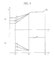
- FIG. 3 includes timing charts showing, in time series, changes in the voltages of the battery banks 21 to 23 and the charging currents corresponding to the respective battery banks 21 to 23 during the charge control implemented by the controller 16.
- the controller 16 first makes a determination as to whether voltage difference ⁇ V of the three battery banks 21 to 23 is larger than a threshold voltage Vx ( FIG. 2 : Step S1).
- the voltage difference ⁇ V here means a deviation of the voltages of the battery banks 21 to 23. More specifically, the voltage difference ⁇ V is difference between the highest and lowest of the voltages of the battery banks 21 to 23.
- the threshold voltage Vx is preferably 0V. In this case, Step S1 determines whether the voltage difference ⁇ V is 0V, that is, whether there is the voltage difference ⁇ V.
- the threshold voltage Vx may be an arbitrary voltage within a range where a determination can be made as to whether there actually is the voltage difference ⁇ V or within a range where a deviation of the voltages of the battery banks 21 to 23 fully charged falls in an allowable range.
- the controller 16 carries out balance charge ( FIG. 2 : Step S2).
- the balance charge means that all the battery banks 21 to 23 are charged while the field effect transistors Tr1, Tr3 and Tr5 are controlled to be on, and the field effect transistors Tr2, Tr4 and Tr6 to be off.
- the balance charge is to charge the battery banks through the charging path in which the DC power outputted by the power source device 11 is supplied to the battery banks 21 to 23 via the current limiting resistors R1 to R3 (first charging path).
- V A , V B and V C the voltages of the battery banks 21, 22 and 23
- I A , I B and I C the charging currents of the battery banks 21, 22 and 23
- the battery banks 21 to 23 In the balance charge, among the battery banks 21 to 23, those having relatively high voltage are relatively low in potential difference generated in the respective current limiting resistors, and are therefore relatively low in charging current, thereby being charged at relatively low speed. In contrast, the battery banks having relatively low voltages are relatively large in potential difference generated in the respective current limiting resistors, and are therefore relatively high in charging current, thereby being charged at relatively high speed. For example, let us assume that, at the start of the charging ( FIG. 3 : timing T1), the voltage V A of the battery bank 21 is a highest voltage value; the voltage V C of the battery bank 23 is a lowest voltage value; and the voltage V B of the battery bank 22 is a substantially middle voltage value between the voltages V A and V C .
- the charging current I C of the battery bank 23 is a relatively highest current; the charging current I A of the battery bank 21 is a relatively lowest current; and the charging current I B of the battery bank 22 is a substantially middle current between the charging currents I C and I A .
- the battery bank 23 is charged at the highest speed, and the battery bank 21 at the lowest speed.
- the battery bank 22 is charged at a substantially middle speed therebetween.
- the voltage difference ⁇ V of the battery banks 21 to 23 is gradually decreased along with the charging of the battery banks 21 to 23.
- the controller 16 carries out normal charge ( FIG. 2 : Step S3).
- the normal charge means that all the battery banks 21 to 23 are charged while the field effect transistors Tr1, Tr3 and Tr5 are controlled to be off, and the field effect transistors Tr2, Tr4 and Tr6 to be on.
- the normal charge is to charge the battery banks through the charging path in which the DC power outputted by the power source device 11 is supplied to the battery banks 21 to 23 without passing through the current limiting resistors R1 to R3 (second charging path).
- the battery banks 21 to 23 are charged at constant current I D through the charging path without the current limiting resistors R1 to R3 (second charging path), so that the charging currents of the battery banks 21 to 23 are equal to each other.
- the battery banks 21 to 23 can be fully charged substantially at a time, and the voltages V A to V C of the battery banks 21 to 23 reach the full charge voltage V D in a minimum time ( FIG. 3 : timing T3). It is thus possible to fully charge all the battery banks 21 to 23 in a minimum time without causing overcharge. More specifically, the controller 16 makes a determination as to whether any one of the voltages V A to V C of the battery banks 21 to 23 has reached the full charge voltage V D ( FIG. 2 : Step S4).
- Step S4 If none of the voltages V A to V C of the battery banks 21 to 23 has reached the full charge voltage V D ( FIG. 2 : the result of Step S4 is NO), the normal charge is continued. At the time point when any one of the voltages V A to V C of the battery banks 21 to 23 reaches the full charge voltage V D ( FIG. 2 : the result of Step S4 is YES), all the field effect transistors Tr1 to Tr6 are controlled to be off, and thus, the charging of the battery banks 21 to 23 is stopped.
- the charger 10 according to the invention is capable of fully charging all the battery banks 21 to 23 of the multi-parallel battery pack 20 without causing overcharge.
- the charge control just uniformly switches the charging paths to one another according to whether there is the voltage difference ⁇ V of the battery banks 21 to 23. For this reason, there is no need for a complicate charge control procedure, so that the first, second and third charging circuits 12, 13 and 14 have very simple constructions, and can be materialized at low costs.
- the invention thus provides at low costs the charger 10 that is capable of fully charging all the battery banks 21 to 23 without causing overcharge.
Landscapes
- Engineering & Computer Science (AREA)
- Power Engineering (AREA)
- Charge And Discharge Circuits For Batteries Or The Like (AREA)
- Secondary Cells (AREA)
Abstract
Description
- The present invention relates to a charger that charges a plurality of batteries all at a time, or more specifically, a charger that charges, for example, a multi-parallel battery pack.
- A common charger that charges a multi-parallel battery pack consisting of a plurality of battery banks is one that finishes the charging at the time point when any one of the battery banks is fully charged, regardless of whether or not the other battery banks are fully charged. At the start of charging, battery banks usually have different state of charge. After any one of the battery banks is fully charged, if the charging is continued until all the other battery banks are fully charged, the first fully charged battery bank will be overcharged and might be deteriorated. For this reason, there is high possibility that a multi-parallel battery pack that is charged by a conventional charger mixedly contains the battery bank fully charged and those not fully charged, or that the state of charge of the battery banks becomes imbalanced. It is then likely that the primary overall battery capacity cannot be retained.
- Among other conventional technologies of charging a multi-parallel battery pack consisting of a plurality of battery banks, a well-known technology is, for example, a charging method that repeatedly charges each battery bank in a multi-parallel battery pack consisting of a plurality of battery banks for a short period of time with an adequately low charging current (See Unexamined Japanese Patent Publication (Kokai) No.
2008-259260 - The imbalance of state of charge of the battery banks in the multi-parallel battery pack can be solved, for example, by detecting a state of full charge of each battery bank and finishing the charging of the battery banks one by one. On the other hand, in order to detect the state of full charge of each battery bank and finish charging the battery banks one by one, it is required to implement charge control on each battery bank. This might complicate the procedure of the control. If the state of full charge is detected with respect to each of the battery banks, and the charging is finished one by one, since the conditions of the battery banks are imbalanced during the charging, there is the possibility that the state of full charge of the battery banks cannot be accurately detected due to interaction of the heat generated in the battery banks.
- The conventional technology disclosed in Unexamined Japanese Patent Publication No.
2008-259260 2008-259260 - The present invention has been made to solve the foregoing problem. It is an object of the invention to provide at low costs a charger that is capable of fully charging a plurality of battery banks without causing overcharge.
- In order to accomplish the above object, the charger of the present invention includes a constant voltage and constant current DC power source; and a battery voltage detection circuit that detects voltages of a plurality of batteries. The charger has a plurality of charging circuits including current limiting resistors, a first charging path that supplies the batteries with DC power that is outputted from the constant voltage and constant DC current power source via the current limiting resistors, a second charging path that supplies the batteries with DC power that is outputted from the constant voltage and constant current power source without passing through the current limiting resistors, and a charging path switching circuit that is capable of selectively switching between the first charging path and the second charging path, the charging circuits being provided to the respective batteries and being identical in resistance values of the current limiting resistors; and a controller that controls the charging circuits so that all the batteries are charged through the first charging path when there is difference in the voltages of the batteries, and that all the batteries are charged through the second charging path when there is no difference in the voltages of the batteries.
- The current limiting resistors disposed in the charging paths are identical in resistance value. When there is difference in the voltages of the batteries, all the batteries are charged through the charging paths equipped with the current limiting resistors corresponding to the respective batteries (first charging path). In this process, the batteries having relatively high voltages (batteries having high state of charge) are relatively small in potential difference (potential difference between the voltage of DC power outputted from the constant voltage and constant current DC power source and the battery voltage) generated in the respective current limiting resistors. In result, the batteries having relatively high voltages are relatively low in charging current, and thus are charged at relatively low speed. In contrast, the batteries having relatively low voltages (batteries having low state of charge) are large in potential difference generated in the respective current limiting resistors, and thus relatively high in charging current, thereby being charged at relatively high speed.
- Consequently, the potential difference between the batteries having relatively high voltages and those having relatively low voltages is gradually reduced as the batteries are charged, leading to a state where there is no difference in the voltages of all the batteries. In short, all the batteries become the same state of charge.
- When there is no difference in the voltages of all the batteries, all the batteries are charged at constant current by using the charging path without a current limiting resistor (second charging path), which equalizes the charging currents of the batteries. All the batteries can therefore be fully charged at a time and reach a state of full charge in a minimum time. It is thus possible to fully charge all the battery banks in a minimum time without causing overcharge.
- The charge control just uniformly switches the charging paths according to whether there is difference in the voltages of the batteries. This reduces costs because there is no need for a complicate charge control procedure, and the charging circuit has a very simple construction.
- Accordingly, the invention provides the operation and advantages of materializing at low costs the charger capable of fully charging all battery banks without causing overcharge.
- According to another aspect of the invention, the charging path switching circuit includes a first switch for turning on/off the first charging path and a second switch for turning on/off the second charging path.
- With the above-mentioned characteristics, the charging path switching circuit is capable of not only selectively switching the first and second charging paths to one another but also stopping the charging by turning off both the first and second switches and thus blocking the supply of the charging current to the batteries.
- The present invention will become more fully understood from the detailed description given hereinafter and the accompanying drawings which are given by way of illustration only, and thus, are not limitative of the present invention, and wherein:
-
FIG. 1 is a view showing a whole configuration of a charger; -
FIG. 2 is a flowchart showing charge control that is implemented by a controller; and -
FIG. 3 includes timing charts showing changes in voltages of battery banks and in charging currents corresponding to the respective battery banks. - An embodiment of the invention will be described below with reference to the attached drawings.
- The configuration of a
charger 10 of the present invention will be described below with reference toFIG. 1 . -
FIG. 1 is a view showing a whole configuration of thecharger 10. - The
charger 10 has apower source device 11, afirst charging circuit 12, asecond charging circuit 13, athird charging circuit 14, a batteryvoltage detection circuit 15 and acontroller 16. Amulti-parallel battery pack 20 charged by thecharger 10 includes threebattery banks 21 to 23. Thebattery banks 21 to 23 are rechargeable batteries such as nickel-hydrogen secondary batteries. The number of battery banks of themulti-parallel battery pack 20 to be charged according to the invention is not particularly limited to three as long as thebattery pack 20 includes two or more battery banks. - The
power source device 11 serving as a "constant voltage and constant current DC power source" is a well-known power source that receives DC power and outputs the DC power of constant voltage and constant current. The DC power outputted by thepower source device 11 is supplied to thebattery banks 21 to 23 of themulti-parallel battery pack 20 through thefirst charging circuit 12, thesecond charging circuit 13 and thethird charging circuit 14. - The
first charging circuit 12 serving as a "charging circuit" corresponds to thebattery bank 21 of themulti-parallel battery pack 20. Thefirst charging circuit 12 includes a current limiting resistor R1 and two field effect transistors (FET) Tr1 and Tr2 forming "charging path switching circuit". The field effect transistor Tr1 serving as a "first switch" and the field effect transistor Tr2 as a "second switch" have drain terminals connected to an output terminal of thepower source device 11. A source terminal of the field effect transistor Tr1 is connected to one end of the current limiting resistor R1. A source terminal of the field effect transistor Tr2 is connected to the other end of the current limiting resistor R1. The field effect transistor Tr1 and the field effect transistor Tr2 have gate terminals connected to thecontroller 16 described later. A connection point of the source terminal of the field effect transistor Tr2 and the other end of the current limiting resistor R1 functions as an output terminal of thefirst charging circuit 12, and is connected to a positive terminal of thebattery bank 21 of themulti-parallel battery pack 20. - The
second charging circuit 13 serving as a "charging circuit" corresponds to thebattery bank 22 of themulti-parallel battery pack 20. Thesecond charging circuit 13 includes a current limiting resistor R2 and two field effect transistors Tr3 and Tr4 forming "charging path switching circuit". The field effect transistor Tr3 serving as a "first switch" and the field effect transistor Tr4 as a "second switch" have drain terminals connected to the output terminal of thepower source device 11. A source terminal of the field effect transistor Tr3 is connected to one end of the current limiting resistor R2. A source terminal of the field effect transistor Tr4 is connected to the other end of the current limiting resistor R2. The field effect transistor Tr3 and the field effect transistor Tr4 have gate terminals connected to thecontroller 16 described later. A connection point of the source terminal of the field effect transistor Tr4 and the other end of the current limiting resistor R2 functions as an output terminal of thesecond charging circuit 13, and is connected to a positive terminal of thebattery bank 22 of themulti-parallel battery pack 20. - The
third charging circuit 14 serving as a "charging circuit" corresponds to thebattery bank 23 of themulti-parallel battery pack 20. Thethird charging circuit 14 includes a current limiting resistor R3 and two field effect transistors Tr5 and Tr6 forming "charging path switching circuit". The field effect transistor Tr5 serving as a "first switch" and the field effect transistor Tr6 as a "second switch" have drain terminals connected to the output terminal of thepower source device 11. A source terminal of the field effect transistor Tr5 is connected to one end of the current limiting resistor R3. A source terminal of the field effect transistor Tr6 is connected to the other end of the current limiting resistor R3. The field effect transistor Tr5 and the field effect transistor Tr6 have gate terminals connected to thecontroller 16 described later. A connection point of the source terminal of the field effect transistor Tr6 and the other end of the current limiting resistor R3 functions as an output terminal of thethird charging circuit 14, and is connected to a positive terminal of thebattery bank 23 of themulti-parallel battery pack 20. - Needless to say, the "first switch" and the "second switch" are not particularly limited to field effect transistors, and may be, for example, electromagnetic relays, solid state relays, bipolar transistors, insulated gate bipolar transistors (IGBT) or the like.
- The DC power outputted by the
power source device 11 in thefirst charging circuit 12 constructed as described above is supplied to thebattery bank 21 via the current limiting resistor R1 when the field effect transistor Tr1 is in an ON state, and the field effect transistor Tr2 in an OFF state (first charging path). When the field effect transistor Tr1 is in the OFF state, and the field effect transistor Tr2 in the ON state, the DC power outputted by thepower source device 11 in thefirst charging circuit 12 is supplied to thebattery bank 21 without passing through the current limiting resistor R1 (second charging path). In other words, if the field effect transistors Tr1 and Tr2 are exclusively turned on/off, thefirst charging circuit 12 can be selectively switched between the charging path with the current limiting resistor R1 (first charging path) and the charging path without the current limiting resistor R1 (second charging path). - Likewise, if the field effect transistors Tr3 and Tr4 are exclusively turned on/off, the
second charging circuit 13 can be selectively switched between the charging path with the current limiting resistor R2 (first charging path) and the charging path without the current limiting resistor R2 (second charging path). If the field effect transistors Tr5 and Tr6 are exclusively turned on/off, thethird charging circuit 14 can be selectively switched between the charging path with the current limiting resistor R3 (first charging path) and the charging path without the current limiting resistor R3 (second charging path). - The current limiting resistor R1 of the
first charging circuit 12, the current limiting resistor R2 of thesecond charging circuit 13, and the current limiting resistor R3 of thethird charging circuit 14 are resistors of identical resistance values. - The battery
voltage detection circuit 15 is a circuit that detects the voltage of each of thebattery banks 21 to 23 of themulti-parallel battery pack 20, and includes six resistors R11 to R16 and three A/D converters 151 to 153. The A/D converters 151 to 153 are well-known analog-digital converters, which convert analog electric signals of voltages of thebattery banks 21 to 23 into digital electric signals, and output the converted signals. - One end of the resistor R11 is connected to the positive terminal of the
battery bank 21 of themulti-parallel battery pack 20. The other end of the resistor R11 is connected to one end of the resistor R12. The other end of the resistor R12 is connected to GND. A connection point of the resistors R11 and R12 is connected to an input terminal of the A/D converter 151. This means that the voltage of thebattery bank 21 is divided by a voltage-dividing circuit formed of the resistors R11 and R12, and then inputted into the input terminal of the A/D converter 151. An output terminal of the A/D converter 151 is connected to thecontroller 16 described later. - One end of the resistor R13 is connected to the positive terminal of the
battery bank 22 of themulti-parallel battery pack 20. The other end of the resistor R13 is connected to one end of the resistor R14. The other end of the resistor R14 is connected to GND. A connection point of the resistors R13 and R14 is connected to an input terminal of the A/D converter 152. That is to say, the voltage of thebattery bank 22 is divided by a voltage-dividing circuit formed of the resistors R13 and R14, and then inputted into the input terminal of the A/D converter 152. An output terminal of the A/D converter 152 is connected to thecontroller 16 described later. - One end of the resistor R15 is connected to the positive terminal of the
battery bank 23 of themulti-parallel battery pack 20. The other end of the resistor R15 is connected to one end of the resistor R16. The other end of the resistor R16 is connected to GND. A connection point of the resistors R15 and R16 is connected to an input terminal of the A/D converter 153. The voltage of thebattery bank 23 is thus divided by a voltage-dividing circuit formed of the resistors R15 and R16, and then inputted into the input terminal of the A/D converter 153. An output terminal of the A/D converter 153 is connected to thecontroller 16 described later. - The
controller 16 includes a well-known microcomputer control circuit. Thecontroller 16 implements ON/OFF control of the field effect transistors Tr1 to Tr6 according to the voltages of thebattery banks 21 to 23 of themulti-parallel battery pack 20, which are detected by the A/D converters 151 to 153. - The charge control implemented by the
controller 16 in thecharger 10 will be described below with reference toFIGS. 2 and3 . -
FIG. 2 is a flowchart showing the charge control implemented by thecontroller 16.FIG. 3 includes timing charts showing, in time series, changes in the voltages of thebattery banks 21 to 23 and the charging currents corresponding to therespective battery banks 21 to 23 during the charge control implemented by thecontroller 16. - Once the charge control of the
multi-parallel battery pack 20 begins, thecontroller 16 first makes a determination as to whether voltage difference ΔV of the threebattery banks 21 to 23 is larger than a threshold voltage Vx (FIG. 2 : Step S1). The voltage difference ΔV here means a deviation of the voltages of thebattery banks 21 to 23. More specifically, the voltage difference ΔV is difference between the highest and lowest of the voltages of thebattery banks 21 to 23. The threshold voltage Vx is preferably 0V. In this case, Step S1 determines whether the voltage difference ΔV is 0V, that is, whether there is the voltage difference ΔV. For example, in consideration of an error in detection of the voltages of thebattery banks 21 to 23, the threshold voltage Vx may be an arbitrary voltage within a range where a determination can be made as to whether there actually is the voltage difference ΔV or within a range where a deviation of the voltages of thebattery banks 21 to 23 fully charged falls in an allowable range. - When the voltage difference ΔV of the
battery banks 21 to 23 is larger than the threshold voltage Vx (FIG. 2 : the result of Step S1 is YES), thecontroller 16 carries out balance charge (FIG. 2 : Step S2). The balance charge means that all thebattery banks 21 to 23 are charged while the field effect transistors Tr1, Tr3 and Tr5 are controlled to be on, and the field effect transistors Tr2, Tr4 and Tr6 to be off. In other words, the balance charge is to charge the battery banks through the charging path in which the DC power outputted by thepower source device 11 is supplied to thebattery banks 21 to 23 via the current limiting resistors R1 to R3 (first charging path). - Hereinafter, the voltages of the
battery banks battery banks - In the balance charge, among the
battery banks 21 to 23, those having relatively high voltage are relatively low in potential difference generated in the respective current limiting resistors, and are therefore relatively low in charging current, thereby being charged at relatively low speed. In contrast, the battery banks having relatively low voltages are relatively large in potential difference generated in the respective current limiting resistors, and are therefore relatively high in charging current, thereby being charged at relatively high speed. For example, let us assume that, at the start of the charging (FIG. 3 : timing T1), the voltage VA of thebattery bank 21 is a highest voltage value; the voltage VC of thebattery bank 23 is a lowest voltage value; and the voltage VB of thebattery bank 22 is a substantially middle voltage value between the voltages VA and VC. In this case, the charging current IC of thebattery bank 23 is a relatively highest current; the charging current IA of thebattery bank 21 is a relatively lowest current; and the charging current IB of thebattery bank 22 is a substantially middle current between the charging currents IC and IA. In comparison, therefore, thebattery bank 23 is charged at the highest speed, and thebattery bank 21 at the lowest speed. Thebattery bank 22 is charged at a substantially middle speed therebetween. The voltage difference ΔV of thebattery banks 21 to 23 is gradually decreased along with the charging of thebattery banks 21 to 23. - When the voltage difference ΔV of the
battery banks 21 to 23 becomes equal to or lower than the threshold voltage Vx (FIG. 2 : the result of Step S1 is NO;FIG. 3 : timing T2), that is, when the state of charge of thebattery banks 21 to 23 become substantially equal, thecontroller 16 carries out normal charge (FIG. 2 : Step S3). The normal charge means that all thebattery banks 21 to 23 are charged while the field effect transistors Tr1, Tr3 and Tr5 are controlled to be off, and the field effect transistors Tr2, Tr4 and Tr6 to be on. In other words, the normal charge is to charge the battery banks through the charging path in which the DC power outputted by thepower source device 11 is supplied to thebattery banks 21 to 23 without passing through the current limiting resistors R1 to R3 (second charging path). - During the normal charge, the
battery banks 21 to 23 are charged at constant current ID through the charging path without the current limiting resistors R1 to R3 (second charging path), so that the charging currents of thebattery banks 21 to 23 are equal to each other. Thebattery banks 21 to 23 can be fully charged substantially at a time, and the voltages VA to VC of thebattery banks 21 to 23 reach the full charge voltage VD in a minimum time (FIG. 3 : timing T3). It is thus possible to fully charge all thebattery banks 21 to 23 in a minimum time without causing overcharge. More specifically, thecontroller 16 makes a determination as to whether any one of the voltages VA to VC of thebattery banks 21 to 23 has reached the full charge voltage VD (FIG. 2 : Step S4). If none of the voltages VA to VC of thebattery banks 21 to 23 has reached the full charge voltage VD (FIG. 2 : the result of Step S4 is NO), the normal charge is continued. At the time point when any one of the voltages VA to VC of thebattery banks 21 to 23 reaches the full charge voltage VD (FIG. 2 : the result of Step S4 is YES), all the field effect transistors Tr1 to Tr6 are controlled to be off, and thus, the charging of thebattery banks 21 to 23 is stopped. - As described above, the
charger 10 according to the invention is capable of fully charging all thebattery banks 21 to 23 of themulti-parallel battery pack 20 without causing overcharge. The charge control just uniformly switches the charging paths to one another according to whether there is the voltage difference ΔV of thebattery banks 21 to 23. For this reason, there is no need for a complicate charge control procedure, so that the first, second andthird charging circuits - The invention thus provides at low costs the
charger 10 that is capable of fully charging all thebattery banks 21 to 23 without causing overcharge.
Claims (2)
- A charger (10) comprising a constant voltage and constant current DC power source (11) and a battery voltage detection circuit (15) that detects voltages of a plurality of batteries (21, 22, 23), characterized in that:the charger (10) has a plurality of charging circuits (12, 13, 14) including current limiting resistors (R1, R2, R3), a first charging path that supplies the batteries (21, 22, 23) with DC power that is outputted from the constant voltage and constant DC current power source (11) via the current limiting resistors (R1, R2, R3), a second charging path that supplies the batteries (21, 22, 23) with DC power that is outputted from the constant voltage and constant current power source (11) without passing through the current limiting resistors (R1, R2, R3), and a charging path switching circuit (Tr1, Tr2, Tr3, Tr4, Tr5 and Tr6) that is capable of selectively switching between the first charging path and the second charging path, the charging circuits (12, 13, 14) being provided to the respective batteries (21, 22, 23) and being identical in resistance values of the current limiting resistors (R1, R2, R3); anda controller (16) that controls the charging circuits (12, 13, 14) so that all the batteries (21, 22, 23) are charged through the first charging path when there is difference in the voltages of the batteries (21, 22, 23), and that all the batteries (21, 22, 23) are charged through the second charging path when there is no difference in the voltages of the batteries (21, 22, 23).
- The charger (10) according to claim 1, characterized in that:the charging path switching circuit (Tr1, Tr2, Tr3, Tr4, Tr5 and Tr6) includes a first switch (Tr1, Tr3, Tr5) for turning on/off the first charging path and a second switch (Tr2, Tr4, Tr6) for turning on/off the second charging path.
Applications Claiming Priority (1)
| Application Number | Priority Date | Filing Date | Title |
|---|---|---|---|
| JP2011107137A JP5714975B2 (en) | 2011-05-12 | 2011-05-12 | Charger |
Publications (3)
| Publication Number | Publication Date |
|---|---|
| EP2523303A2 true EP2523303A2 (en) | 2012-11-14 |
| EP2523303A3 EP2523303A3 (en) | 2014-05-14 |
| EP2523303B1 EP2523303B1 (en) | 2016-04-06 |
Family
ID=46085410
Family Applications (1)
| Application Number | Title | Priority Date | Filing Date |
|---|---|---|---|
| EP12167342.0A Not-in-force EP2523303B1 (en) | 2011-05-12 | 2012-05-09 | Charger |
Country Status (4)
| Country | Link |
|---|---|
| US (1) | US9048668B2 (en) |
| EP (1) | EP2523303B1 (en) |
| JP (1) | JP5714975B2 (en) |
| CN (1) | CN102780242B (en) |
Cited By (2)
| Publication number | Priority date | Publication date | Assignee | Title |
|---|---|---|---|---|
| EP2784904A3 (en) * | 2013-03-15 | 2015-04-01 | Samsung Electro-Mechanics Co., Ltd. | Power charging apparatus and battery apparatus |
| EP3700047A3 (en) * | 2019-02-19 | 2020-10-28 | Samsung Electronics Co., Ltd. | Method of controlling charging of plurality of batteries and electronic device to which the same is applied |
Families Citing this family (53)
| Publication number | Priority date | Publication date | Assignee | Title |
|---|---|---|---|---|
| US9882403B2 (en) * | 2012-11-23 | 2018-01-30 | Htc Corporation | Battery module |
| CN103779903A (en) * | 2014-01-23 | 2014-05-07 | 昆山市圣光新能源科技有限公司 | Novel portable automobile emergency ignition power source with Bluetooth and distress signal lamp |
| CN103779924A (en) * | 2014-02-09 | 2014-05-07 | 昆山市圣光新能源科技有限公司 | Novel antiskid portable automobile emergency ignition power source with MP3 function and flashlight function |
| CN103779933A (en) * | 2014-02-09 | 2014-05-07 | 昆山市圣光新能源科技有限公司 | Novel antiskid portable automobile emergency ignition power source with charging function and MP3 function |
| JP2015154593A (en) * | 2014-02-14 | 2015-08-24 | ソニー株式会社 | Charge/discharge control device, battery pack, electronic apparatus, electric motor vehicle and charge/discharge control method |
| CN103779940A (en) * | 2014-02-18 | 2014-05-07 | 昆山市圣光新能源科技有限公司 | Novel portable automobile emergency ignition power source with radio and liquid crystal display panel |
| CN104953696B (en) * | 2014-03-27 | 2019-06-28 | 伊顿制造(格拉斯哥)有限合伙莫尔日分支机构 | Line interaction uninterruptible power supply |
| CN105939979B (en) | 2014-03-28 | 2019-06-28 | 积水化学工业株式会社 | Interlayer film for laminated glass and laminated glass |
| CN105098852A (en) * | 2014-05-09 | 2015-11-25 | 株式会社日立制作所 | Electric automobile battery changing device and charge management method thereof |
| CN104113104B (en) * | 2014-05-22 | 2017-01-04 | 深圳天珑无线科技有限公司 | A kind of charging method and system |
| CN104052126A (en) * | 2014-06-30 | 2014-09-17 | 昆山市圣光新能源科技有限公司 | Novel double-wire car emergency ignition power supply with charging and Bluetooth functions |
| CN105337320A (en) * | 2014-06-30 | 2016-02-17 | 展讯通信(上海)有限公司 | Dynamic current charging method and circuit |
| CN105322591B (en) * | 2014-08-01 | 2018-05-04 | 联想移动通信科技有限公司 | A kind of method, apparatus and electronic equipment for showing the electronic equipment charging interval |
| CN104242394A (en) * | 2014-09-23 | 2014-12-24 | 重庆星联云科科技发展有限公司 | Active equalization circuit and equalization method of series batteries |
| CN104410144B (en) * | 2014-11-24 | 2017-07-14 | 华为技术有限公司 | The circuit and equipment powered for HVDC |
| CN104410137B (en) * | 2014-12-26 | 2017-05-24 | 青岛歌尔声学科技有限公司 | Charging protection circuit and electronic product |
| CN105071521B (en) * | 2015-08-19 | 2017-09-05 | 青岛海尔空调器有限总公司 | The method for controlling power supply and air conditioner of air conditioner |
| CN105119334A (en) * | 2015-08-31 | 2015-12-02 | 深圳驿普乐氏科技有限公司 | Voltage transformation circuit with wide voltage output range and DC charging pile |
| CN205039569U (en) * | 2015-09-02 | 2016-02-17 | 国网上海市电力公司 | Lithium ion battery organizes balanced management system |
| CN105305586A (en) * | 2015-09-30 | 2016-02-03 | 天津中聚新能源科技有限公司 | Photovoltaic control protector |
| CN105262166B (en) * | 2015-10-21 | 2018-05-01 | 王震 | A kind of Multifunctional portable power source |
| CN105207266B (en) * | 2015-10-26 | 2019-01-08 | 苏州华安普电力科技股份有限公司 | A kind of distribution roof photovoltaic power generation intelligent energy storage system |
| CN105245009A (en) * | 2015-10-28 | 2016-01-13 | 杨之扬 | Electric equipment networking manager |
| CN105305562B (en) * | 2015-11-25 | 2018-06-26 | 成都迅能达电源科技有限公司 | Accumulator is internalized into charge and discharge device and is internalized into charging/discharging apparatus |
| CN105471027A (en) * | 2015-12-15 | 2016-04-06 | 云南电网有限责任公司电力科学研究院 | Super-capacitor pre-charging system |
| CN106130087B (en) * | 2016-04-15 | 2018-12-07 | 安徽正熹标王新能源有限公司 | A kind of vehicle multifunction mobile power source |
| CN109038748B (en) * | 2016-04-15 | 2021-12-28 | 深圳市贝视特科技有限公司 | Portable power supply provided with heating device |
| CN106100004B (en) * | 2016-04-15 | 2018-12-21 | 新昌县鼎瑞科技有限公司 | A kind of low-temperature resistance multifunction charging device |
| CN105871009A (en) * | 2016-04-28 | 2016-08-17 | 黄永怀 | Central storage battery for emergency lamps in warehouse |
| CN107332294A (en) * | 2016-04-29 | 2017-11-07 | 宇龙计算机通信科技(深圳)有限公司 | A kind of charging device |
| CN106160068B (en) * | 2016-05-17 | 2018-12-21 | 新昌县鼎瑞科技有限公司 | A kind of vehicle multifunction emergency power supply |
| CN106100010B (en) * | 2016-05-17 | 2018-12-21 | 新昌县鼎瑞科技有限公司 | A kind of Vehicular multifunctional backup power source |
| CN106160069B (en) * | 2016-05-17 | 2018-12-21 | 新昌县鼎瑞科技有限公司 | A kind of Vehicular multifunctional mobile power source |
| CN105978068A (en) * | 2016-05-26 | 2016-09-28 | 江苏深苏电子科技有限公司 | Charging and discharging management system of lithium battery |
| CN105914870A (en) * | 2016-06-01 | 2016-08-31 | 上海应用技术学院 | Communication base station stand-by power supply system based on activation-type cell and wind-solar complementary power supply system |
| CN105978119A (en) * | 2016-07-14 | 2016-09-28 | 广西电网有限责任公司柳州供电局 | Intelligent emergency power supply |
| CN105978109B (en) * | 2016-07-15 | 2018-11-27 | 东莞健达照明有限公司 | A kind of secondary cell charger used for mobile power source |
| JP6883396B2 (en) * | 2016-08-25 | 2021-06-09 | 矢崎総業株式会社 | Quick charging device |
| CN106253402A (en) * | 2016-08-26 | 2016-12-21 | 吴桐光 | A kind of electric automobile charging station based on WIFI network |
| CN106100077A (en) * | 2016-08-26 | 2016-11-09 | 吴桐光 | A kind of charging system of networking |
| CN106100143A (en) * | 2016-08-26 | 2016-11-09 | 吴桐光 | A kind of long distance wireless charging system |
| CN106253406A (en) * | 2016-08-31 | 2016-12-21 | 成都国蓉科技有限公司 | A kind of wireless charging terminal under water |
| CN106451465B (en) * | 2016-09-30 | 2018-11-13 | 国家电网公司 | It is a kind of to be used for the new energy model splicing method based on CIM in AVC controls |
| CN106340958A (en) * | 2016-10-25 | 2017-01-18 | 中国海洋石油总公司 | Diesel generator type offshore platform emergency power supply and distribution device |
| CN106329707A (en) * | 2016-10-25 | 2017-01-11 | 中国海洋石油总公司 | Emergency power system of offshore platform |
| CN106786944B (en) * | 2016-12-31 | 2020-12-18 | 华为技术有限公司 | A sampling circuit, equalization circuit and system of single cells in series battery pack |
| WO2019041100A1 (en) * | 2017-08-28 | 2019-03-07 | 深圳市大疆创新科技有限公司 | Charging system and charging method |
| WO2019111872A1 (en) * | 2017-12-04 | 2019-06-13 | 株式会社Gsユアサ | Charging control device, electricity storage device, and charging method |
| CN110247541A (en) * | 2018-03-08 | 2019-09-17 | 鸿富锦精密电子(天津)有限公司 | It can inhibit the power supply circuit of dash current |
| TW202011660A (en) * | 2018-09-07 | 2020-03-16 | 飛宏科技股份有限公司 | Multi-channel intelligent charger |
| KR20230039565A (en) * | 2021-09-14 | 2023-03-21 | 에이블릭 가부시키가이샤 | Cell balance circuit, cell balance device, charge/discharge control circuit, charge/discharge control device, and battery device |
| US12549023B2 (en) | 2021-12-08 | 2026-02-10 | Samsung Electronics Co., Ltd. | Electronic device comprising a plurality of batteries and method for protecting the batteries in the same |
| EP4372959A4 (en) * | 2022-09-30 | 2025-04-30 | Samsung Electronics Co., Ltd. | ELECTRONIC DEVICE WITH MULTIPLE BATTERIES AND OPERATING METHOD THEREFOR |
Citations (1)
| Publication number | Priority date | Publication date | Assignee | Title |
|---|---|---|---|---|
| JP2008259260A (en) | 2007-04-02 | 2008-10-23 | Matsushita Electric Ind Co Ltd | How to charge the power supply |
Family Cites Families (9)
| Publication number | Priority date | Publication date | Assignee | Title |
|---|---|---|---|---|
| JP3069498B2 (en) * | 1994-09-01 | 2000-07-24 | 富士通株式会社 | Charge / discharge device and electronic equipment |
| JPH08213055A (en) * | 1995-02-08 | 1996-08-20 | Honda Motor Co Ltd | Method and device for charging assembled battery |
| US5985100A (en) * | 1995-08-30 | 1999-11-16 | Basf Aktiengesellschaft | Process for separating butanol and dibutyl ether by means of dual-pressure distillation |
| JP4572850B2 (en) * | 2006-03-24 | 2010-11-04 | 株式会社日立製作所 | Power control device |
| JP5020530B2 (en) * | 2006-04-14 | 2012-09-05 | パナソニック株式会社 | Charging method, battery pack and charger thereof |
| JP2008220104A (en) * | 2007-03-06 | 2008-09-18 | Canon Inc | A charging device and a charging control method for the charging device. |
| JP5342860B2 (en) * | 2008-12-12 | 2013-11-13 | 株式会社日立製作所 | Power storage device having current balance function |
| TWI379486B (en) * | 2009-02-17 | 2012-12-11 | Green Solution Tech Co Ltd | The battery charging controlling apparatus and battery balance charging controller |
| JP5478174B2 (en) * | 2009-09-24 | 2014-04-23 | 北陸電力株式会社 | Charging method and system for large secondary battery |
-
2011
- 2011-05-12 JP JP2011107137A patent/JP5714975B2/en active Active
-
2012
- 2012-05-09 EP EP12167342.0A patent/EP2523303B1/en not_active Not-in-force
- 2012-05-09 US US13/467,559 patent/US9048668B2/en active Active
- 2012-05-11 CN CN201210147512.1A patent/CN102780242B/en not_active Expired - Fee Related
Patent Citations (1)
| Publication number | Priority date | Publication date | Assignee | Title |
|---|---|---|---|---|
| JP2008259260A (en) | 2007-04-02 | 2008-10-23 | Matsushita Electric Ind Co Ltd | How to charge the power supply |
Cited By (4)
| Publication number | Priority date | Publication date | Assignee | Title |
|---|---|---|---|---|
| EP2784904A3 (en) * | 2013-03-15 | 2015-04-01 | Samsung Electro-Mechanics Co., Ltd. | Power charging apparatus and battery apparatus |
| US9502910B2 (en) | 2013-03-15 | 2016-11-22 | Samsung Electro-Mechanics Co., Ltd. | Power charging apparatus and battery apparatus |
| EP3700047A3 (en) * | 2019-02-19 | 2020-10-28 | Samsung Electronics Co., Ltd. | Method of controlling charging of plurality of batteries and electronic device to which the same is applied |
| US11855456B2 (en) | 2019-02-19 | 2023-12-26 | Samsung Electronics Co., Ltd. | Method of controlling charging of plurality of batteries and electronic device to which the same is applied |
Also Published As
| Publication number | Publication date |
|---|---|
| CN102780242B (en) | 2016-01-20 |
| EP2523303A3 (en) | 2014-05-14 |
| JP5714975B2 (en) | 2015-05-07 |
| EP2523303B1 (en) | 2016-04-06 |
| CN102780242A (en) | 2012-11-14 |
| JP2012239326A (en) | 2012-12-06 |
| US9048668B2 (en) | 2015-06-02 |
| US20120286722A1 (en) | 2012-11-15 |
Similar Documents
| Publication | Publication Date | Title |
|---|---|---|
| EP2523303B1 (en) | Charger | |
| US7804276B2 (en) | Circuit arrangement and method for transferring electrical charge between accumulators of an accumulator arrangement including a series circuit of accumulators | |
| US8633677B2 (en) | Battery pack and method of charging battery pack | |
| US7714544B2 (en) | Switching device for bi-directionally equalizing charge between energy accumulators and corresponding methods | |
| US6836095B2 (en) | Battery charging method and apparatus | |
| EP2418751B1 (en) | Battery charger and battery charging method | |
| US20050017676A1 (en) | Portable device and semiconductor device | |
| US9106081B2 (en) | Secondary cell protection circuit and battery | |
| US20010054880A1 (en) | Charge/discharge control circuit and secondary battery | |
| JP2011004509A (en) | Charge control circuit, battery pack, and charging system | |
| US20080136264A1 (en) | Charging apparatus | |
| JP6370137B2 (en) | Charge / discharge control circuit and battery device | |
| JP6824295B2 (en) | Electrical equipment | |
| EP3893353B1 (en) | Battery polarity determination circuit, charger, and electronic device | |
| JP5165405B2 (en) | Charge control circuit, battery pack, and charging system | |
| JP3581428B2 (en) | Rechargeable power supply | |
| JP2004129439A (en) | Voltage equalization device for backup power supply device | |
| JPH08103027A (en) | Battery pack status detector | |
| WO2013035238A1 (en) | Voltage balance correction circuit | |
| JP2022535476A (en) | FET controller and method | |
| JP7325613B2 (en) | Power supply device and assembled battery charging method | |
| JP2020092566A (en) | Charger and charging method | |
| US9184612B2 (en) | Battery charging circuit | |
| CN115811104A (en) | Cell balancing circuit and device, charge and discharge control circuit and device and battery device | |
| JP4110858B2 (en) | Abnormality detection device for battery pack |
Legal Events
| Date | Code | Title | Description |
|---|---|---|---|
| PUAI | Public reference made under article 153(3) epc to a published international application that has entered the european phase |
Free format text: ORIGINAL CODE: 0009012 |
|
| AK | Designated contracting states |
Kind code of ref document: A2 Designated state(s): AL AT BE BG CH CY CZ DE DK EE ES FI FR GB GR HR HU IE IS IT LI LT LU LV MC MK MT NL NO PL PT RO RS SE SI SK SM TR |
|
| AX | Request for extension of the european patent |
Extension state: BA ME |
|
| PUAL | Search report despatched |
Free format text: ORIGINAL CODE: 0009013 |
|
| AK | Designated contracting states |
Kind code of ref document: A3 Designated state(s): AL AT BE BG CH CY CZ DE DK EE ES FI FR GB GR HR HU IE IS IT LI LT LU LV MC MK MT NL NO PL PT RO RS SE SI SK SM TR |
|
| AX | Request for extension of the european patent |
Extension state: BA ME |
|
| RIC1 | Information provided on ipc code assigned before grant |
Ipc: H02J 7/00 20060101AFI20140408BHEP |
|
| 17P | Request for examination filed |
Effective date: 20141024 |
|
| RBV | Designated contracting states (corrected) |
Designated state(s): AL AT BE BG CH CY CZ DE DK EE ES FI FR GB GR HR HU IE IS IT LI LT LU LV MC MK MT NL NO PL PT RO RS SE SI SK SM TR |
|
| RAP1 | Party data changed (applicant data changed or rights of an application transferred) |
Owner name: FDK CORPORATION |
|
| GRAP | Despatch of communication of intention to grant a patent |
Free format text: ORIGINAL CODE: EPIDOSNIGR1 |
|
| INTG | Intention to grant announced |
Effective date: 20151111 |
|
| GRAS | Grant fee paid |
Free format text: ORIGINAL CODE: EPIDOSNIGR3 |
|
| RAP1 | Party data changed (applicant data changed or rights of an application transferred) |
Owner name: FDK CORPORATION |
|
| GRAA | (expected) grant |
Free format text: ORIGINAL CODE: 0009210 |
|
| AK | Designated contracting states |
Kind code of ref document: B1 Designated state(s): AL AT BE BG CH CY CZ DE DK EE ES FI FR GB GR HR HU IE IS IT LI LT LU LV MC MK MT NL NO PL PT RO RS SE SI SK SM TR |
|
| REG | Reference to a national code |
Ref country code: GB Ref legal event code: FG4D |
|
| REG | Reference to a national code |
Ref country code: AT Ref legal event code: REF Ref document number: 788717 Country of ref document: AT Kind code of ref document: T Effective date: 20160415 Ref country code: CH Ref legal event code: EP |
|
| REG | Reference to a national code |
Ref country code: IE Ref legal event code: FG4D |
|
| REG | Reference to a national code |
Ref country code: DE Ref legal event code: R096 Ref document number: 602012016492 Country of ref document: DE |
|
| REG | Reference to a national code |
Ref country code: FR Ref legal event code: PLFP Year of fee payment: 5 |
|
| REG | Reference to a national code |
Ref country code: LT Ref legal event code: MG4D Ref country code: NL Ref legal event code: MP Effective date: 20160406 |
|
| REG | Reference to a national code |
Ref country code: AT Ref legal event code: MK05 Ref document number: 788717 Country of ref document: AT Kind code of ref document: T Effective date: 20160406 |
|
| PG25 | Lapsed in a contracting state [announced via postgrant information from national office to epo] |
Ref country code: BE Free format text: LAPSE BECAUSE OF NON-PAYMENT OF DUE FEES Effective date: 20160531 |
|
| PG25 | Lapsed in a contracting state [announced via postgrant information from national office to epo] |
Ref country code: NL Free format text: LAPSE BECAUSE OF FAILURE TO SUBMIT A TRANSLATION OF THE DESCRIPTION OR TO PAY THE FEE WITHIN THE PRESCRIBED TIME-LIMIT Effective date: 20160406 |
|
| PG25 | Lapsed in a contracting state [announced via postgrant information from national office to epo] |
Ref country code: LT Free format text: LAPSE BECAUSE OF FAILURE TO SUBMIT A TRANSLATION OF THE DESCRIPTION OR TO PAY THE FEE WITHIN THE PRESCRIBED TIME-LIMIT Effective date: 20160406 Ref country code: NO Free format text: LAPSE BECAUSE OF FAILURE TO SUBMIT A TRANSLATION OF THE DESCRIPTION OR TO PAY THE FEE WITHIN THE PRESCRIBED TIME-LIMIT Effective date: 20160706 Ref country code: FI Free format text: LAPSE BECAUSE OF FAILURE TO SUBMIT A TRANSLATION OF THE DESCRIPTION OR TO PAY THE FEE WITHIN THE PRESCRIBED TIME-LIMIT Effective date: 20160406 Ref country code: PL Free format text: LAPSE BECAUSE OF FAILURE TO SUBMIT A TRANSLATION OF THE DESCRIPTION OR TO PAY THE FEE WITHIN THE PRESCRIBED TIME-LIMIT Effective date: 20160406 Ref country code: IS Free format text: LAPSE BECAUSE OF FAILURE TO SUBMIT A TRANSLATION OF THE DESCRIPTION OR TO PAY THE FEE WITHIN THE PRESCRIBED TIME-LIMIT Effective date: 20160806 |
|
| PG25 | Lapsed in a contracting state [announced via postgrant information from national office to epo] |
Ref country code: PT Free format text: LAPSE BECAUSE OF FAILURE TO SUBMIT A TRANSLATION OF THE DESCRIPTION OR TO PAY THE FEE WITHIN THE PRESCRIBED TIME-LIMIT Effective date: 20160808 Ref country code: GR Free format text: LAPSE BECAUSE OF FAILURE TO SUBMIT A TRANSLATION OF THE DESCRIPTION OR TO PAY THE FEE WITHIN THE PRESCRIBED TIME-LIMIT Effective date: 20160707 Ref country code: RS Free format text: LAPSE BECAUSE OF FAILURE TO SUBMIT A TRANSLATION OF THE DESCRIPTION OR TO PAY THE FEE WITHIN THE PRESCRIBED TIME-LIMIT Effective date: 20160406 Ref country code: AT Free format text: LAPSE BECAUSE OF FAILURE TO SUBMIT A TRANSLATION OF THE DESCRIPTION OR TO PAY THE FEE WITHIN THE PRESCRIBED TIME-LIMIT Effective date: 20160406 Ref country code: SE Free format text: LAPSE BECAUSE OF FAILURE TO SUBMIT A TRANSLATION OF THE DESCRIPTION OR TO PAY THE FEE WITHIN THE PRESCRIBED TIME-LIMIT Effective date: 20160406 Ref country code: HR Free format text: LAPSE BECAUSE OF FAILURE TO SUBMIT A TRANSLATION OF THE DESCRIPTION OR TO PAY THE FEE WITHIN THE PRESCRIBED TIME-LIMIT Effective date: 20160406 Ref country code: LV Free format text: LAPSE BECAUSE OF FAILURE TO SUBMIT A TRANSLATION OF THE DESCRIPTION OR TO PAY THE FEE WITHIN THE PRESCRIBED TIME-LIMIT Effective date: 20160406 Ref country code: ES Free format text: LAPSE BECAUSE OF FAILURE TO SUBMIT A TRANSLATION OF THE DESCRIPTION OR TO PAY THE FEE WITHIN THE PRESCRIBED TIME-LIMIT Effective date: 20160406 |
|
| PG25 | Lapsed in a contracting state [announced via postgrant information from national office to epo] |
Ref country code: BE Free format text: LAPSE BECAUSE OF FAILURE TO SUBMIT A TRANSLATION OF THE DESCRIPTION OR TO PAY THE FEE WITHIN THE PRESCRIBED TIME-LIMIT Effective date: 20160406 Ref country code: IT Free format text: LAPSE BECAUSE OF FAILURE TO SUBMIT A TRANSLATION OF THE DESCRIPTION OR TO PAY THE FEE WITHIN THE PRESCRIBED TIME-LIMIT Effective date: 20160406 |
|
| REG | Reference to a national code |
Ref country code: CH Ref legal event code: PL |
|
| REG | Reference to a national code |
Ref country code: DE Ref legal event code: R097 Ref document number: 602012016492 Country of ref document: DE |
|
| PG25 | Lapsed in a contracting state [announced via postgrant information from national office to epo] |
Ref country code: SK Free format text: LAPSE BECAUSE OF FAILURE TO SUBMIT A TRANSLATION OF THE DESCRIPTION OR TO PAY THE FEE WITHIN THE PRESCRIBED TIME-LIMIT Effective date: 20160406 Ref country code: EE Free format text: LAPSE BECAUSE OF FAILURE TO SUBMIT A TRANSLATION OF THE DESCRIPTION OR TO PAY THE FEE WITHIN THE PRESCRIBED TIME-LIMIT Effective date: 20160406 Ref country code: LI Free format text: LAPSE BECAUSE OF NON-PAYMENT OF DUE FEES Effective date: 20160531 Ref country code: RO Free format text: LAPSE BECAUSE OF FAILURE TO SUBMIT A TRANSLATION OF THE DESCRIPTION OR TO PAY THE FEE WITHIN THE PRESCRIBED TIME-LIMIT Effective date: 20160406 Ref country code: DK Free format text: LAPSE BECAUSE OF FAILURE TO SUBMIT A TRANSLATION OF THE DESCRIPTION OR TO PAY THE FEE WITHIN THE PRESCRIBED TIME-LIMIT Effective date: 20160406 Ref country code: MC Free format text: LAPSE BECAUSE OF FAILURE TO SUBMIT A TRANSLATION OF THE DESCRIPTION OR TO PAY THE FEE WITHIN THE PRESCRIBED TIME-LIMIT Effective date: 20160406 Ref country code: CZ Free format text: LAPSE BECAUSE OF FAILURE TO SUBMIT A TRANSLATION OF THE DESCRIPTION OR TO PAY THE FEE WITHIN THE PRESCRIBED TIME-LIMIT Effective date: 20160406 Ref country code: CH Free format text: LAPSE BECAUSE OF NON-PAYMENT OF DUE FEES Effective date: 20160531 |
|
| PLBE | No opposition filed within time limit |
Free format text: ORIGINAL CODE: 0009261 |
|
| STAA | Information on the status of an ep patent application or granted ep patent |
Free format text: STATUS: NO OPPOSITION FILED WITHIN TIME LIMIT |
|
| REG | Reference to a national code |
Ref country code: IE Ref legal event code: MM4A |
|
| PG25 | Lapsed in a contracting state [announced via postgrant information from national office to epo] |
Ref country code: SM Free format text: LAPSE BECAUSE OF FAILURE TO SUBMIT A TRANSLATION OF THE DESCRIPTION OR TO PAY THE FEE WITHIN THE PRESCRIBED TIME-LIMIT Effective date: 20160406 |
|
| 26N | No opposition filed |
Effective date: 20170110 |
|
| REG | Reference to a national code |
Ref country code: FR Ref legal event code: PLFP Year of fee payment: 6 |
|
| PG25 | Lapsed in a contracting state [announced via postgrant information from national office to epo] |
Ref country code: IE Free format text: LAPSE BECAUSE OF NON-PAYMENT OF DUE FEES Effective date: 20160509 Ref country code: SI Free format text: LAPSE BECAUSE OF FAILURE TO SUBMIT A TRANSLATION OF THE DESCRIPTION OR TO PAY THE FEE WITHIN THE PRESCRIBED TIME-LIMIT Effective date: 20160406 |
|
| REG | Reference to a national code |
Ref country code: FR Ref legal event code: PLFP Year of fee payment: 7 |
|
| PG25 | Lapsed in a contracting state [announced via postgrant information from national office to epo] |
Ref country code: HU Free format text: LAPSE BECAUSE OF FAILURE TO SUBMIT A TRANSLATION OF THE DESCRIPTION OR TO PAY THE FEE WITHIN THE PRESCRIBED TIME-LIMIT; INVALID AB INITIO Effective date: 20120509 Ref country code: CY Free format text: LAPSE BECAUSE OF FAILURE TO SUBMIT A TRANSLATION OF THE DESCRIPTION OR TO PAY THE FEE WITHIN THE PRESCRIBED TIME-LIMIT Effective date: 20160406 |
|
| PG25 | Lapsed in a contracting state [announced via postgrant information from national office to epo] |
Ref country code: MT Free format text: LAPSE BECAUSE OF NON-PAYMENT OF DUE FEES Effective date: 20160531 Ref country code: MK Free format text: LAPSE BECAUSE OF FAILURE TO SUBMIT A TRANSLATION OF THE DESCRIPTION OR TO PAY THE FEE WITHIN THE PRESCRIBED TIME-LIMIT Effective date: 20160406 Ref country code: LU Free format text: LAPSE BECAUSE OF NON-PAYMENT OF DUE FEES Effective date: 20160509 Ref country code: TR Free format text: LAPSE BECAUSE OF FAILURE TO SUBMIT A TRANSLATION OF THE DESCRIPTION OR TO PAY THE FEE WITHIN THE PRESCRIBED TIME-LIMIT Effective date: 20160406 |
|
| PG25 | Lapsed in a contracting state [announced via postgrant information from national office to epo] |
Ref country code: BG Free format text: LAPSE BECAUSE OF FAILURE TO SUBMIT A TRANSLATION OF THE DESCRIPTION OR TO PAY THE FEE WITHIN THE PRESCRIBED TIME-LIMIT Effective date: 20160406 |
|
| PG25 | Lapsed in a contracting state [announced via postgrant information from national office to epo] |
Ref country code: AL Free format text: LAPSE BECAUSE OF FAILURE TO SUBMIT A TRANSLATION OF THE DESCRIPTION OR TO PAY THE FEE WITHIN THE PRESCRIBED TIME-LIMIT Effective date: 20160406 |
|
| REG | Reference to a national code |
Ref country code: FR Ref legal event code: PLFP Year of fee payment: 12 |
|
| PGFP | Annual fee paid to national office [announced via postgrant information from national office to epo] |
Ref country code: GB Payment date: 20230330 Year of fee payment: 12 |
|
| P01 | Opt-out of the competence of the unified patent court (upc) registered |
Effective date: 20230517 |
|
| PGFP | Annual fee paid to national office [announced via postgrant information from national office to epo] |
Ref country code: FR Payment date: 20230411 Year of fee payment: 12 Ref country code: DE Payment date: 20230331 Year of fee payment: 12 |
|
| REG | Reference to a national code |
Ref country code: DE Ref legal event code: R119 Ref document number: 602012016492 Country of ref document: DE |
|
| GBPC | Gb: european patent ceased through non-payment of renewal fee |
Effective date: 20240509 |
|
| PG25 | Lapsed in a contracting state [announced via postgrant information from national office to epo] |
Ref country code: DE Free format text: LAPSE BECAUSE OF NON-PAYMENT OF DUE FEES Effective date: 20241203 |
|
| PG25 | Lapsed in a contracting state [announced via postgrant information from national office to epo] |
Ref country code: FR Free format text: LAPSE BECAUSE OF NON-PAYMENT OF DUE FEES Effective date: 20240531 |
|
| PG25 | Lapsed in a contracting state [announced via postgrant information from national office to epo] |
Ref country code: GB Free format text: LAPSE BECAUSE OF NON-PAYMENT OF DUE FEES Effective date: 20240509 |