EP2521194A1 - Method for manufacturing a magnetoresistive element - Google Patents
Method for manufacturing a magnetoresistive element Download PDFInfo
- Publication number
- EP2521194A1 EP2521194A1 EP10841058A EP10841058A EP2521194A1 EP 2521194 A1 EP2521194 A1 EP 2521194A1 EP 10841058 A EP10841058 A EP 10841058A EP 10841058 A EP10841058 A EP 10841058A EP 2521194 A1 EP2521194 A1 EP 2521194A1
- Authority
- EP
- European Patent Office
- Prior art keywords
- layer
- metal layer
- metal
- substrate
- oxidized
- Prior art date
- Legal status (The legal status is an assumption and is not a legal conclusion. Google has not performed a legal analysis and makes no representation as to the accuracy of the status listed.)
- Granted
Links
Images



Classifications
-
- G—PHYSICS
- G11—INFORMATION STORAGE
- G11B—INFORMATION STORAGE BASED ON RELATIVE MOVEMENT BETWEEN RECORD CARRIER AND TRANSDUCER
- G11B5/00—Recording by magnetisation or demagnetisation of a record carrier; Reproducing by magnetic means; Record carriers therefor
- G11B5/127—Structure or manufacture of heads, e.g. inductive
- G11B5/33—Structure or manufacture of flux-sensitive heads, i.e. for reproduction only; Combination of such heads with means for recording or erasing only
- G11B5/39—Structure or manufacture of flux-sensitive heads, i.e. for reproduction only; Combination of such heads with means for recording or erasing only using magneto-resistive devices or effects
-
- B—PERFORMING OPERATIONS; TRANSPORTING
- B82—NANOTECHNOLOGY
- B82Y—SPECIFIC USES OR APPLICATIONS OF NANOSTRUCTURES; MEASUREMENT OR ANALYSIS OF NANOSTRUCTURES; MANUFACTURE OR TREATMENT OF NANOSTRUCTURES
- B82Y10/00—Nanotechnology for information processing, storage or transmission, e.g. quantum computing or single electron logic
-
- B—PERFORMING OPERATIONS; TRANSPORTING
- B82—NANOTECHNOLOGY
- B82Y—SPECIFIC USES OR APPLICATIONS OF NANOSTRUCTURES; MEASUREMENT OR ANALYSIS OF NANOSTRUCTURES; MANUFACTURE OR TREATMENT OF NANOSTRUCTURES
- B82Y25/00—Nanomagnetism, e.g. magnetoimpedance, anisotropic magnetoresistance, giant magnetoresistance or tunneling magnetoresistance
-
- G—PHYSICS
- G01—MEASURING; TESTING
- G01R—MEASURING ELECTRIC VARIABLES; MEASURING MAGNETIC VARIABLES
- G01R33/00—Arrangements or instruments for measuring magnetic variables
- G01R33/02—Measuring direction or magnitude of magnetic fields or magnetic flux
- G01R33/06—Measuring direction or magnitude of magnetic fields or magnetic flux using galvano-magnetic devices
- G01R33/09—Magnetoresistive devices
- G01R33/093—Magnetoresistive devices using multilayer structures, e.g. giant magnetoresistance sensors
-
- G—PHYSICS
- G01—MEASURING; TESTING
- G01R—MEASURING ELECTRIC VARIABLES; MEASURING MAGNETIC VARIABLES
- G01R33/00—Arrangements or instruments for measuring magnetic variables
- G01R33/02—Measuring direction or magnitude of magnetic fields or magnetic flux
- G01R33/06—Measuring direction or magnitude of magnetic fields or magnetic flux using galvano-magnetic devices
- G01R33/09—Magnetoresistive devices
- G01R33/098—Magnetoresistive devices comprising tunnel junctions, e.g. tunnel magnetoresistance sensors
-
- G—PHYSICS
- G11—INFORMATION STORAGE
- G11B—INFORMATION STORAGE BASED ON RELATIVE MOVEMENT BETWEEN RECORD CARRIER AND TRANSDUCER
- G11B5/00—Recording by magnetisation or demagnetisation of a record carrier; Reproducing by magnetic means; Record carriers therefor
- G11B5/127—Structure or manufacture of heads, e.g. inductive
- G11B5/33—Structure or manufacture of flux-sensitive heads, i.e. for reproduction only; Combination of such heads with means for recording or erasing only
- G11B5/39—Structure or manufacture of flux-sensitive heads, i.e. for reproduction only; Combination of such heads with means for recording or erasing only using magneto-resistive devices or effects
- G11B5/3903—Structure or manufacture of flux-sensitive heads, i.e. for reproduction only; Combination of such heads with means for recording or erasing only using magneto-resistive devices or effects using magnetic thin film layers or their effects, the films being part of integrated structures
- G11B5/3906—Details related to the use of magnetic thin film layers or to their effects
-
- G—PHYSICS
- G11—INFORMATION STORAGE
- G11B—INFORMATION STORAGE BASED ON RELATIVE MOVEMENT BETWEEN RECORD CARRIER AND TRANSDUCER
- G11B5/00—Recording by magnetisation or demagnetisation of a record carrier; Reproducing by magnetic means; Record carriers therefor
- G11B5/127—Structure or manufacture of heads, e.g. inductive
- G11B5/33—Structure or manufacture of flux-sensitive heads, i.e. for reproduction only; Combination of such heads with means for recording or erasing only
- G11B5/39—Structure or manufacture of flux-sensitive heads, i.e. for reproduction only; Combination of such heads with means for recording or erasing only using magneto-resistive devices or effects
- G11B5/3903—Structure or manufacture of flux-sensitive heads, i.e. for reproduction only; Combination of such heads with means for recording or erasing only using magneto-resistive devices or effects using magnetic thin film layers or their effects, the films being part of integrated structures
- G11B5/3906—Details related to the use of magnetic thin film layers or to their effects
- G11B5/3909—Arrangements using a magnetic tunnel junction
-
- H—ELECTRICITY
- H10—SEMICONDUCTOR DEVICES; ELECTRIC SOLID-STATE DEVICES NOT OTHERWISE PROVIDED FOR
- H10N—ELECTRIC SOLID-STATE DEVICES NOT OTHERWISE PROVIDED FOR
- H10N50/00—Galvanomagnetic devices
- H10N50/01—Manufacture or treatment
-
- C—CHEMISTRY; METALLURGY
- C08—ORGANIC MACROMOLECULAR COMPOUNDS; THEIR PREPARATION OR CHEMICAL WORKING-UP; COMPOSITIONS BASED THEREON
- C08K—Use of inorganic or non-macromolecular organic substances as compounding ingredients
- C08K2201/00—Specific properties of additives
- C08K2201/01—Magnetic additives
Definitions
- the present invention relates to a manufacturing method of a magneto-resistive element exhibiting a high MR ratio.
- a tunneling magneto-resistive (TMR) element has a structure in which a tunnel barrier layer is sandwiched between two ferromagnetic layers. When an external magnetic field is applied and the relative magnetization angle between the two ferromagnetic layers is changed, the tunneling conduction probability of an electron through the tunnel barrier layer is changed and the resistance of the TMR element is changed.
- TMR element is applied to a read-out sensor part of a magnetic head used for a hard disk and a device such as a nonvolatile memory MRAM utilizing magnetism.
- An oxide of aluminum (Al), titanium (Ti), magnesium (Mg), or the like is used as a material for the tunnel barrier layer of the TMR element.
- a magnesium oxide (MgO) tunnel barrier layer can have a larger magneto-resistance change rate (MR ratio) (refer to non-patent document 1).
- Manufacturing methods of the MgO tunnel barrier layer include a method of forming the MgO layer directly by radio-frequency (RF) sputtering of an MgO target and a method of depositing an Mg layer and thereafter forming the MgO layer by oxidation treatment.
- RF radio-frequency
- a method for a TMR element using the method of forming the MgO tunnel barrier layer directly by the RF sputtering of the MgO target, a method is disclosed (refer to non-patent document 2), which performs substrate heating after the formation of the MgO tunnel barrier layer, as a technique to improve the MR ratio particularly for a low RA (element resistance x element area).
- a method is disclosed (refer to patent document 1), which after depositing a first Mg layer, forms an MgO layer on the surface of the Mg layer by natural oxidation, and then deposits a second Mg layer, thereby forming a tunnel barrier layer including the first Mg layer/ MgO layer/ second Mg layer.
- a method which after depositing a first Mg layer, performs oxidation treatment under a high pressure, thereafter deposits a second Mg layer and performs oxidation treatment under a low pressure (refer to patent document 2).
- a stacked body of a first MgO layer and a second MgO layer as the tunnel barrier layer (refer to patent document 3).
- a first Mg layer is formed and a first MgO layer is formed by oxidation of the first Mg layer.
- the first MgO layer is caused to have a crystalline orientation by annealing of the first MgO layer in a magnetic field.
- a second Mg layer is formed on the fist MgO layer and the second Mg layer is oxidized to form a second MgO layer, and thus a tunnel barrier layer is formed as the stacked body of the first MgO layer and the second MgO layer.
- the present invention aims at providing a manufacturing method of a magneto-resistive effect element capable of obtaining a higher MR ratio in a method of forming a metal oxide layer (e.g., MgO layer) by performing oxidation treatment on a metal layer (e.g., Mg layer).
- a metal oxide layer e.g., MgO layer
- a first aspect of the present invention is a manufacturing method of a magneto-resistive element, including a step of providing a substrate on which a first ferromagnetic layer is formed, a step of fabricating a tunnel barrier layer on the first ferromagnetic layer, and a step of forming a second ferromagnetic layer on the tunnel barrier layer, and the step of fabricating the tunnel barrier layer includes a step of depositing a first metal layer on the first ferromagnetic layer, a step of oxidizing the first metal layer, a step of depositing a second metal layer on the oxidized first metal layer, and a step of performing heating treatment on the oxidized first metal layer and the second metal layer.
- a second aspect of the present invention is a manufacturing method of a magneto-resistive element, including a step of providing a substrate on which a first ferromagnetic layer is formed, a step of fabricating a tunnel barrier layer on the first ferromagnetic layer, and a step of forming a second ferromagnetic layer on the tunnel barrier layer, and the step of fabricating the tunnel barrier layer includes a step of depositing a first metal layer on the first ferromagnetic layer, a step of oxidizing the first metal layer, a step of depositing a second metal layer on the oxidized first metal layer, and a step of performing heating treatment on the oxidized first metal layer and the second metal layer at a temperature at which the second metal layer boils.
- FIG. 1 is a flowchart explaining manufacturing steps of a TMR element according to the present embodiment. Further, FIG. 2 is a cross-sectional view schematically showing a configuration of the TMR element according to the present embodiment.
- an underlayer 2 having a first underlayer 2a and a second underlayer 2b and a fixed magnetization layer 4 are deposited on a processing substrate 1 in step S1.
- the underlayer configured with tantalum (Ta), hafnium (Hf), niobium (Nb), zirconium (Zr), titanium (Ti), molybdenum (Mo), tungsten (W), or the like, for example, is deposited having a thickness of approximately 0.5 to 5 nm on the processing substrate 1 as the first underlayer 2a of the multi-layered film.
- a ferromagnetic layer 4a which has a thickness of approximately 1 to 5 nm and is configured with CoFe or the like, for example, a nonmagnetic intermediate layer 4b which has a thickness of approximately 0.8 nm and is configured with an alloy including at least one of or two or more of Ru, Cr, rhodium (Rh), iridium (Tr), and rhenium (Re), and a ferromagnetic layer 4c which has a thickness of approximately 1 to 5 nm and is configured with CoFe, CoFeB, or the like, for example, are deposited thereon.
- the anti-ferromagnetic layer 3, the ferromagnetic layer 4a, the nonmagnetic intermediate layer 4b, and the ferromagnetic layer 4c form a synthetic-type fixed magnetization layer 4.
- the ferromagnetic layers 4a and 4c and the nonmagnetic intermediate layer 4b may be replaced by a single layer of a ferromagnetic layer.
- the fixed magnetization layer 4 has a two-layer structure of the anti-ferromagnetic layer 3 and the ferromagnetic layer.
- the fixed magnetization layer 4 is formed over the substrate 1 in step S1 it is optional to use a substrate 1 over which the fixed magnetization layer 4 is preliminarily deposited. That is, in the present embodiment, any method may be used if a substrate can be provided having a ferromagnetic layer on which a tunnel barrier layer is to be formed.
- a first metal layer 5a is deposited in approximately 0.5 to 2.0 nm on the fixed magnetization layer 4.
- Mg is preferable from the viewpoint of obtaining a high MR ratio, and Zn or an alloy of Mg and Zn is also preferable.
- the first metal layer 5a may be an alloy containing Mg.
- the first metal layer 5a may be a metal such as Al, Ti, Zn, Hf and Ga. Moreover, oxygen may be added to the above metal illustrated as the first metal layer 5a (refer to a second embodiment), or at least one of non-metal such as boron (B), and carbon (C) may be added.
- non-metal such as boron (B), and carbon (C)
- the substrate 1 over which the first metal layer 5a is formed is transferred to an oxidation chamber and the first metal layer 5a is oxidized.
- the oxidation treatment is performed by oxygen gas or oxygen gas and inert gas, for example, at least one of helium (He), neon (Ne), argon (Ar), krypton (Kr), and xenon (Xe).
- the oxidation may be performed by a method of confined oxidation which performs in the confined chamber, flow oxidation during exhaustion, radical oxidation utilizing active oxygen, plasma oxidation, or the like.
- step S4 the substrate 1 over which the first metal layer 5a is oxidized is transferred to a film deposition chamber and a second metal layer 5b is deposited on the above oxidized first metal layer 5a.
- This layer has a function to prevent or reduce the oxidation of the magnetization free layer, which is caused by the movement of oxygen remaining on the surface of the oxidized first metal layer 5a to the magnetization free layer to be formed successively.
- Mg is preferable as the second metal layer 5b from the viewpoint of obtaining a high MR ratio. Otherwise, a metal of Ti, Zn, Hf, or the like may be used.
- step S5 the substrate 1 over which the oxidized first metal layer 5a and the second metal layer 5b are formed is transferred to a heating chamber and heating treatment is applied thereto. That is, in the present embodiment, the heating treatment is performed after the deposition of the second metal layer 5b and also before the magnetization free layer 6 to be described below is deposited. The heating treatment promotes binding between the metal and oxygen and has an effect of enabling the barrier layer to have a more uniform and higher grade film quality. Moreover, in the present embodiment, the second metal layer 5b is evaporated by the heating treatment.
- the heating treatment causes oxygen and the like which remain in the oxidation of the first metal layer 5a and exist between the first metal layer 5a and the second metal layer 5b, to react with the second metal layer 5b and oxidizes the second metal layer 5b.
- the present embodiment removes the metal component which is not oxidized in the oxidation of the second metal layer 5b by evaporating the non-oxidized second metal layer 5b (metal component of the second metal layer 5b which has not been bound to oxygen in the heating treatment of the present step).
- the heating treatment in the present step has the function of oxidizing the second metal layer 5b and evaporating the metal component which remains without being involved in the oxidation, in addition to the function of crystallizing the metal oxide.
- the heating temperature is a temperature at which the second metal layer 5b is vaporized (temperature at which vaporization occurs), that is, a temperature at which evaporation of the second metal layer 5b occurs.
- the heating temperature is preferably 150 to 400 degrees as a substrate temperature.
- the binding between Mg as metal and oxygen is not promoted sufficiently and also the evaporation of Mg is not perfect.
- the boiling of Mg starts at approximately 423K (approximately 150°C) in an atmosphere of 1 ⁇ 10 -9 to 1 ⁇ 10 -8 Torr.
- Mg which is not bound to oxygen boils at a temperature equal to or higher than approximately 150°C in an atmosphere of 1 ⁇ 10 -9 to 1 ⁇ 10 -8 Torr, and this Mg is vaporized, and thereby Mg which is not bound to oxygen is removed from the oxide of the second metal layer 5b.
- the temperature equal to or higher than 150°C is preferable for the evaporation of Mg.
- the synthetic antiferro coupling of the fixed magnetization layer 4 is deteriorated.
- the heating treatment may be performed so as to cause the first and second metal layers 5a and 5b to be heated at a temperature at which the metal to be used evaporates according to the setting pressure utilizing a temperature dependence on vapor pressure as shown in FIG. 8 .
- a preferable heating method is a method of utilizing radiation such as a heat generation resistor or a lamp heater, or a method of disposing a wafer directly on a heated stage and utilizing heat conduction. Moreover, also other heating methods may be used.
- the present step forms the tunnel barrier layer 5 having the oxidized first metal layer 5a and the oxidized second metal layer 5b.
- step S6 the substrate 1 heat-treated in step S5 is transferred to a film deposition chamber and a magnetization free layer 6 configured with at least one layer or two or more layers of CoFe, CoFeB, NiFe and the like is deposited in approximately 1 to 10 nm. Meanwhile, a cooling step may be performed before the deposition of the magnetization free layer 6 for the purpose of preventing diffusion between the tunnel barrier layer 5 and the magnetization free layer 6.
- the substrate may be cooled down to a temperature equal to or lower than 150 degrees.
- a protection layer 7 configured with at least one layer or two or more layers of Ta, Ru, Ti, Pt, and the like is deposited on the magnetization free layer 6 in approximately 1 to 30 nm.
- Such a TMR element is fabricated consistently in vacuum with the use of a cluster-type substrate treatment apparatus as shown in FIG. 3 .
- At least one or more film deposition chambers, one oxidation chamber, and one substrate heating chamber are necessary for fabricating the TMR element of the present embodiment.
- the substrate 1 transferred from a load-lock chamber 8 is transferred to a film deposition chamber 9a, and the underlayer 2 to the ferromagnetic layer 4c shown in FIG. 2 are deposited on the substrate 1.
- the substrate 1 is transferrer to a film deposition chamber 9b and the first metal layer 5a (e.g., first Mg layer) is deposited.
- the substrate 1 over which the first metal layer 5a is formed is transferred to an oxidation chamber 10 and the first metal layer 5a is oxidized.
- the substrate 1 over which the first metal layer 5a is oxidized is returned to the film deposition chamber 9b and the second metal layer 5b (e.g., second Mg layer) is deposited on the oxidized first metal layer 5a.
- the substrate 1 over which the second metal layer 5b is formed is transferred to a heating chamber 11 and substrate heating treatment is performed.
- the heat-treated substrate 1 is returned to the film deposition chamber 9b and the magnetization free layer 6 and the protection layer 7 are deposited.
- all of the load-lock chamber 8, the film deposition chambers 9a and 9b, the oxidation chamber 10, and the heating chamber 11 are connected to one another via a transfer chamber 12.
- Each of the chambers is provided with an individual exhausting device and can be exhausted independently, and thereby the substrate treatment can be performed consistently in vacuum.
- a cooling chamber may be provided for cooling after the substrate heating treatment and the substrate may be cooled before the deposition of the magnetization free layer 6.
- the substrate may be cooled within the film deposition chamber before the deposition of the magnetization free layer 6.
- the above described TMR element can be used for a read-out sensor of a hard disk magnetic head, a storage cell of an MRAM, and other magnetic sensors.
- a manufacturing method of a TMR element capable of obtaining a high MR ratio will be explained for the TMR element using the method of depositing the metal layer and thereafter forming the oxidation layer by oxidation treatment in the above described present embodiment.
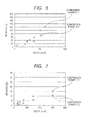
- Mg was used for the first metal layer 5a and a first Mg layer was deposited in 1.2 nm as the first metal layer 5a. After that, the first Mg layer was oxidized and Mg (second Mg layer) was deposited in 0.4 nm as the second metal layer 5b. After that, TMR elements were fabricated and RA and TMR ratios were measured for the case in which the substrate heating treatment (step S5 of FIG. 1 ) was performed at a temperature at which the second Mg layer evaporates (example 1) and the case of not performing the substrate heating treatment (comparison example 1). In the substrate heating treatment, a resistor was caused to generate heat and the substrate was heated by radiation. The substrate temperature was approximately 300 degrees. The result is shown in FIG. 4 . Further, RA was changed by the change of oxidation time and a result of a relationship between the oxidation time and RA is shown in FIG. 5 .
- FIG. 6 shows relationships between RA and the MR ratio for an element obtained when the timing of the substrate heating treatment was changed (comparison example 2) and for the element obtained in the above comparison example 1.
- the first Mg layer is deposited, the first Mg layer is oxidized after that, the substrate heating treatment is performed, and then the second Mg layer is deposited.
- FIG. 7 shows a relationship between the oxidation time and RA for the TMR element fabricated in this condition.
- the substrate heating treatment is performed, and the second Mg layer is deposited after the heating treatment as in the comparison example 2, for the timing of the substrate heating treatment, it is found that the element characteristic is deteriorated compared to the comparison example 1. This would be caused by that surplus oxygen atoms exist after the oxidation treatment in the vicinity of the surface of the MgO layer formed from the first Mg layer (first metal layer 5a) and the MgO is excessively oxidized or the ferromagnetic layer thereunder is oxidized by the heating treatment applied thereto, resulting in the characteristic deterioration.
- the result of the comparison example 1 would be similarly caused by that surplus oxygen atoms exist after the oxidation treatment on the surface of the MgO layer formed from the first Mg layer and thereby an MgO layer having a good crystalline quality is not obtained and the characteristic is deteriorated.
- the second Mg layer is deposited after the oxidation treatment of the first Mg layer and then the heating treatment is performed. Therefore, the surplus oxygen atoms existing in the vicinity of the MgO layer surface (i.e., boundary surface between the oxidized first metal layer 5a and the second metal layer 5b formed on the first metal layer 5a) and the second Mg layer (second metal layer 5b) react with each other to form a MgO layer. That is, by the substrate heating treatment (step S5) of the present example, oxygen existing at the above boundary surface is bound to Mg of the second Mg layer to convert the second Mg layer into MgO.
- the formation of the MgO layer and the crystallization of MgO are promoted by performing the substrate heating treatment and a MgO layer having a good crystalline quality in which a stoichiometric proportion of Mg:O is close to 1:1 is obtained, and thereby the good result was presumably obtained compared to the comparison examples.
- the present embodiment by forming the first metal layer 5a, oxidizing the first metal layer 5a, then forming the second metal layer 5b on the oxidized first metal layer 5a, and thereafter performing the substrate heating treatment, it is possible to reduce the influence of oxygen inevitably remaining in the vicinity of the metal layer surface on the MR ratio when oxidizing the metal layer which is the original material of the tunnel barrier layer.
- the second metal layer 5b is formed after the oxidation of the first metal layer 5a and the heating treatment is performed in the state in which oxygen exists at the boundary surface between the first metal layer 5a and the second metal layer 5b, and thereby it is possible to use the oxygen remaining in the vicinity of the metal layer surface, which caused the deterioration of the MR ratio conventionally, for the oxidation of the second metal layer 5b and resultantly it is possible to obtain an effect equivalent to the effect of removing the oxygen existing at the above boundary surface.
- This oxidation is caused by the oxygen existing at the above boundary surface and therefore it is possible to eliminate or reduce the oxygen remaining on the surface of the oxidized first metal layer 5a.
- the heating temperature causing the above oxidation is set to a temperature at which the evaporation of the second metal layer 5b occurs, and thereby non-oxidized components are vaporized and removed in the second metal layer 5b and it is possible to form a metal oxide in which oxygen remaining on the surface is reduced.
- the positions of the magnetization free layer 6 and the fixed magnetization layer 4 are described limitedly in the above described embodiment and examples, the positions of the magnetization free layer 6 and the fixed magnetization layer 4 are not particularly specified in the present invention. That is, the magnetization free layer 6 may be formed on the lower side of the tunnel barrier layer 5 and the fixed magnetization layer 4 may be formed on the upper side of the tunnel barrier layer 5.
- the first metal layer 5a intentionally contains oxygen elements in the formation of the first metal layer 5a (the first metal layer 5a is doped with oxygen). That is, in the present embodiment, in the formation of the first metal layer 5a, oxygen gas is also introduced into the film deposition chamber and the first metal layer 5a is formed while oxygen is contained therein.
- the fist metal layer 5a when the fist metal layer 5a is deposited by plasma sputtering, it is possible to cause the first metal layer 5a to contain oxygen atoms therein by adding oxygen to plasma formation gas in step S2 of FIG. 1 . That is, a target of metal (e.g., Mg) which becomes the material of the first metal layer 5a is provided in the film deposition chamber, inert gas is introduced into the film deposition chamber and plasma is generated, and the first metal layer 5a is formed over the substrate 1 by plasma sputtering of the above target.
- oxygen gas is introduced into the film deposition chamber in addition to the inert gas. At this time, the supplied oxygen gas may be or may not be excited into plasma.
- sputter particles e.g., Mg particles
- oxygen oxygen ion or oxygen radical when excited into plasma
- the timing to introduce the oxygen gas for the above oxygen doping may be the same as or may be different from the timing to introduce the inert gas of the sputtering gas. Further, the timing to terminate the oxygen gas supply may be the same as or may be different from the timing to terminate the inert gas supply.
- Mg When Mg is used as the first metal layer 5a and Ar gas is used as the inert gas, for example, Mg may be deposited as the first metal layer 5a in an atmosphere in which Ar gas and oxygen gas are introduced independently from each other in 15 sccm and 5 sccm, respectively (mixed oxygen concentration is 25%), for example.
- the first metal layer 5a contains oxygen, and thereby it is possible to perform the oxidation of the first metal layer 5a preferably also in the vicinity of the boundary surface between the first metal layer 5a and the ferromagnetic layer 4c which is the lower layer of the first metal layer 5a.
- control of the oxidation needs to be performed strictly for oxidizing the second layer in the vicinity of the boundary surface with the first layer. If the oxidation is excessively strong, the first layer is also oxidized, and, if the oxidation is excessively weak, a non-oxidized part remains in the second layer.
- the oxygen distributes in the thickness direction of the first metal layer 5a formed on the ferromagnetic layer 4c and oxygen exists also in the vicinity of the boundary surface with the ferromagnetic layer 4c within the first metal layer 5a. Accordingly, in the oxidation treatment of step S3, oxygen preliminarily contained in the first metal layer 5a contributes to the oxidation of the first metal layer 5a, and therefore the oxidation is performed preferably also in the vicinity of the boundary surface of the first metal layer 5a by the oxygen contained in the first metal layer 5a. Therefore, a good quality metal oxide (e.g., MgO) caused by the first metal layer 5a can be formed also at the boundary surface between the first metal layer 5a and the ferromagnetic layer 4c.
- MgO metal oxide
Landscapes
- Engineering & Computer Science (AREA)
- Physics & Mathematics (AREA)
- Chemical & Material Sciences (AREA)
- Manufacturing & Machinery (AREA)
- Nanotechnology (AREA)
- Crystallography & Structural Chemistry (AREA)
- General Physics & Mathematics (AREA)
- Condensed Matter Physics & Semiconductors (AREA)
- Mathematical Physics (AREA)
- Theoretical Computer Science (AREA)
- Hall/Mr Elements (AREA)
- Mram Or Spin Memory Techniques (AREA)
- Magnetic Heads (AREA)
Abstract
Description
- The present invention relates to a manufacturing method of a magneto-resistive element exhibiting a high MR ratio.
- A tunneling magneto-resistive (TMR) element has a structure in which a tunnel barrier layer is sandwiched between two ferromagnetic layers. When an external magnetic field is applied and the relative magnetization angle between the two ferromagnetic layers is changed, the tunneling conduction probability of an electron through the tunnel barrier layer is changed and the resistance of the TMR element is changed. Such a TMR element is applied to a read-out sensor part of a magnetic head used for a hard disk and a device such as a nonvolatile memory MRAM utilizing magnetism.
- An oxide of aluminum (Al), titanium (Ti), magnesium (Mg), or the like is used as a material for the tunnel barrier layer of the TMR element. Particularly a magnesium oxide (MgO) tunnel barrier layer can have a larger magneto-resistance change rate (MR ratio) (refer to non-patent document 1).
- Manufacturing methods of the MgO tunnel barrier layer include a method of forming the MgO layer directly by radio-frequency (RF) sputtering of an MgO target and a method of depositing an Mg layer and thereafter forming the MgO layer by oxidation treatment.
- For a TMR element using the method of forming the MgO tunnel barrier layer directly by the RF sputtering of the MgO target, a method is disclosed (refer to non-patent document 2), which performs substrate heating after the formation of the MgO tunnel barrier layer, as a technique to improve the MR ratio particularly for a low RA (element resistance x element area).
- Further, for a TMR element using the method of depositing the Mg layer and forming the MgO layer by the oxidation treatment, a method is disclosed (refer to patent document 1), which after depositing a first Mg layer, forms an MgO layer on the surface of the Mg layer by natural oxidation, and then deposits a second Mg layer, thereby forming a tunnel barrier layer including the first Mg layer/ MgO layer/ second Mg layer.
As another method, there is disclosed a method which after depositing a first Mg layer, performs oxidation treatment under a high pressure, thereafter deposits a second Mg layer and performs oxidation treatment under a low pressure (refer to patent document 2). - Moreover, it is disclosed to form a stacked body of a first MgO layer and a second MgO layer as the tunnel barrier layer (refer to patent document 3). In the method disclosed in
patent document 3, first, a first Mg layer is formed and a first MgO layer is formed by oxidation of the first Mg layer. Then, the first MgO layer is caused to have a crystalline orientation by annealing of the first MgO layer in a magnetic field. Successively, a second Mg layer is formed on the fist MgO layer and the second Mg layer is oxidized to form a second MgO layer, and thus a tunnel barrier layer is formed as the stacked body of the first MgO layer and the second MgO layer. -
- Patent document 1 : Japanese Patent Application Laid-Open Publication No.
2007-142424 - Patent document 2: Japanese Patent Application Laid-Open Publication No.
2007-305768 - Patent document 3: Japanese Patent Application Laid-Open Publication No.
2007-173843 -
- Non-patent document 1: Butler et al., Physical Review B, 63, 054416 (2001)
- Non-patent document 2: Appl. Phys. Lett., 93-192109
- While generally a higher MR ratio can be obtained by the formation method of performing the RF sputtering of the MgO target, there is a problem that a lot of particles are generated in this method. When the particles fall on a region corresponding to an TMR element on a wafer, there arises a problem that electrical characteristics of the TMR element are deteriorated.
- Meanwhile, in the method of forming the Mg layer and thereafter forming the MgO layer by the oxidation treatment, while particles are scarcely generated and this method is suitable for volume production compared to the method of performing RF sputtering of the MgO target, there is a problem that the MR ratio is small. The MR ratios obtained by the methods disclosed by the above patent documents are 34% in
patent document 1 and approximately 60% inpatent document 3. - Accordingly, the present invention aims at providing a manufacturing method of a magneto-resistive effect element capable of obtaining a higher MR ratio in a method of forming a metal oxide layer (e.g., MgO layer) by performing oxidation treatment on a metal layer (e.g., Mg layer).
- For achieving such an object, a first aspect of the present invention is a manufacturing method of a magneto-resistive element, including a step of providing a substrate on which a first ferromagnetic layer is formed, a step of fabricating a tunnel barrier layer on the first ferromagnetic layer, and a step of forming a second ferromagnetic layer on the tunnel barrier layer, and the step of fabricating the tunnel barrier layer includes a step of depositing a first metal layer on the first ferromagnetic layer, a step of oxidizing the first metal layer, a step of depositing a second metal layer on the oxidized first metal layer, and a step of performing heating treatment on the oxidized first metal layer and the second metal layer.
- A second aspect of the present invention is a manufacturing method of a magneto-resistive element, including a step of providing a substrate on which a first ferromagnetic layer is formed, a step of fabricating a tunnel barrier layer on the first ferromagnetic layer, and a step of forming a second ferromagnetic layer on the tunnel barrier layer, and the step of fabricating the tunnel barrier layer includes a step of depositing a first metal layer on the first ferromagnetic layer, a step of oxidizing the first metal layer, a step of depositing a second metal layer on the oxidized first metal layer, and a step of performing heating treatment on the oxidized first metal layer and the second metal layer at a temperature at which the second metal layer boils.
- According to the present invention, it is possible to provide a magneto-resistive element having a stall number of particles and a high MR ratio.
-
-
FIG. 1 is a flowchart explaining TMR element manufacturing steps according to an embodiment of the present invention. -
FIG. 2 is a cross-sectional view schematically showing a configuration of a TMR element manufactured by the method ofFIG. 1 . -
FIG. 3 is a diagram showing a configuration of a manufacturing apparatus for fabricating a TMR element according to an embodiment of the present invention. -
FIG. 4 is a characteristic chart showing relationships between RA and a MR ratio for a case of performing substrate heating treatment after the deposition of a second Mg layer and a case of not performing the substrate heating treatment, according to an embodiment of the present invention. -
FIG. 5 is a characteristic chart showing relationships between oxidation time and RA for a case of performing substrate heating treatment after the deposition of a second Mg layer and a case of not performing the substrate heating treatment, according to an embodiment of the present invention. -
FIG. 6 is a characteristic chart showing relationships between RA and a MR ratio for a case of performing substrate heating treatment after oxidation treatment and a case of not performing the substrate heating treatment, according to an embodiment of the present invention. -
FIG. 7 is a characteristic chart showing relationships between oxidation time and RA for a case of performing substrate heating treatment after oxidation treatment and a case of not performing the substrate heating treatment, according to an embodiment of the present invention. -
FIG. 8 is a diagram showing an Mg temperature dependence on vapor pressure according to an embodiment of the present invention. -
FIG. 1 is a flowchart explaining manufacturing steps of a TMR element according to the present embodiment. Further,FIG. 2 is a cross-sectional view schematically showing a configuration of the TMR element according to the present embodiment. - First, as shown in
FIG. 1 , anunderlayer 2 having afirst underlayer 2a and asecond underlayer 2b and afixed magnetization layer 4 are deposited on aprocessing substrate 1 in step S1. For example, the underlayer configured with tantalum (Ta), hafnium (Hf), niobium (Nb), zirconium (Zr), titanium (Ti), molybdenum (Mo), tungsten (W), or the like, for example, is deposited having a thickness of approximately 0.5 to 5 nm on theprocessing substrate 1 as thefirst underlayer 2a of the multi-layered film. Thesecond underlayer 2b containing at least one of elements such as nickel (Ni), iron (Fe), chromium (Cr), and ruthenium (Ru), for example, is deposited thereon in approximately 0.5 to 5 nm. Ananti-ferromagnetic layer 3 configured with IrMn, PtMn, FeMn, NiMn, RuRhMn, CrPtMn, or the like, for example, is deposited thereon in approximately 3 to 15 nm.
Note that, while, in the present embodiment, the stacked body of thefirst underlayer 2a and thesecond underlayer 2b are used as theunderlayer 2, theunderlayer 2 is not limited to this case and theunderlayer 2 may be a single layer. - A
ferromagnetic layer 4a which has a thickness of approximately 1 to 5 nm and is configured with CoFe or the like, for example, a nonmagneticintermediate layer 4b which has a thickness of approximately 0.8 nm and is configured with an alloy including at least one of or two or more of Ru, Cr, rhodium (Rh), iridium (Tr), and rhenium (Re), and aferromagnetic layer 4c which has a thickness of approximately 1 to 5 nm and is configured with CoFe, CoFeB, or the like, for example, are deposited thereon. Theanti-ferromagnetic layer 3, theferromagnetic layer 4a, the nonmagneticintermediate layer 4b, and theferromagnetic layer 4c form a synthetic-type fixedmagnetization layer 4. Theferromagnetic layers intermediate layer 4b may be replaced by a single layer of a ferromagnetic layer. In this case, thefixed magnetization layer 4 has a two-layer structure of theanti-ferromagnetic layer 3 and the ferromagnetic layer. - While, in the present embodiment, the
fixed magnetization layer 4 is formed over thesubstrate 1 in step S1 it is optional to use asubstrate 1 over which thefixed magnetization layer 4 is preliminarily deposited. That is, in the present embodiment, any method may be used if a substrate can be provided having a ferromagnetic layer on which a tunnel barrier layer is to be formed. - In step S2, a
first metal layer 5a is deposited in approximately 0.5 to 2.0 nm on thefixed magnetization layer 4. As thefirst metal layer 5a, Mg is preferable from the viewpoint of obtaining a high MR ratio, and Zn or an alloy of Mg and Zn is also preferable. Alternatively, thefirst metal layer 5a may be an alloy containing Mg. - Otherwise, the
first metal layer 5a may be a metal such as Al, Ti, Zn, Hf and Ga. Moreover, oxygen may be added to the above metal illustrated as thefirst metal layer 5a (refer to a second embodiment), or at least one of non-metal such as boron (B), and carbon (C) may be added. - After that, in step S3, the
substrate 1 over which thefirst metal layer 5a is formed is transferred to an oxidation chamber and thefirst metal layer 5a is oxidized. The oxidation treatment is performed by oxygen gas or oxygen gas and inert gas, for example, at least one of helium (He), neon (Ne), argon (Ar), krypton (Kr), and xenon (Xe). The oxidation may be performed by a method of confined oxidation which performs in the confined chamber, flow oxidation during exhaustion, radical oxidation utilizing active oxygen, plasma oxidation, or the like. - After that, in step S4, the
substrate 1 over which thefirst metal layer 5a is oxidized is transferred to a film deposition chamber and asecond metal layer 5b is deposited on the above oxidizedfirst metal layer 5a. This layer has a function to prevent or reduce the oxidation of the magnetization free layer, which is caused by the movement of oxygen remaining on the surface of the oxidizedfirst metal layer 5a to the magnetization free layer to be formed successively. Mg is preferable as thesecond metal layer 5b from the viewpoint of obtaining a high MR ratio. Otherwise, a metal of Ti, Zn, Hf, or the like may be used. - After that, in step S5, the
substrate 1 over which the oxidizedfirst metal layer 5a and thesecond metal layer 5b are formed is transferred to a heating chamber and heating treatment is applied thereto. That is, in the present embodiment, the heating treatment is performed after the deposition of thesecond metal layer 5b and also before the magnetizationfree layer 6 to be described below is deposited. The heating treatment promotes binding between the metal and oxygen and has an effect of enabling the barrier layer to have a more uniform and higher grade film quality. Moreover, in the present embodiment, thesecond metal layer 5b is evaporated by the heating treatment. In the present embodiment, as described above, the heating treatment causes oxygen and the like which remain in the oxidation of thefirst metal layer 5a and exist between thefirst metal layer 5a and thesecond metal layer 5b, to react with thesecond metal layer 5b and oxidizes thesecond metal layer 5b. At this time, the present embodiment removes the metal component which is not oxidized in the oxidation of thesecond metal layer 5b by evaporating the non-oxidizedsecond metal layer 5b (metal component of thesecond metal layer 5b which has not been bound to oxygen in the heating treatment of the present step). Accordingly, the heating treatment in the present step has the function of oxidizing thesecond metal layer 5b and evaporating the metal component which remains without being involved in the oxidation, in addition to the function of crystallizing the metal oxide. Accordingly, the heating temperature is a temperature at which thesecond metal layer 5b is vaporized (temperature at which vaporization occurs), that is, a temperature at which evaporation of thesecond metal layer 5b occurs. - For example, when Mg is used as the first and
second metal layers FIG. 8 , for the case of Mg, the boiling of Mg starts at approximately 423K (approximately 150°C) in an atmosphere of 1 × 10⁻⁹ to 1 × 10⁻⁸ Torr. Accordingly, in thesecond metal layer 5b, Mg which is not bound to oxygen boils at a temperature equal to or higher than approximately 150°C in an atmosphere of 1 × 10⁻⁹ to 1 × 10⁻⁸ Torr, and this Mg is vaporized, and thereby Mg which is not bound to oxygen is removed from the oxide of thesecond metal layer 5b. In this manner, the temperature equal to or higher than 150°C is preferable for the evaporation of Mg. Further, at a temperature equal to or higher than 400 degrees, the synthetic antiferro coupling of the fixedmagnetization layer 4 is deteriorated. - In this manner, by employing a temperature at which Mg boils as a heating temperature in the heating treatment of the
second metal layer 5b, it is possible to more efficiently vaporize Mg which is not bound to oxygen. That is, it is possible to remove Mg efficiently. Further, by the efficient removal of Mg, it is possible to reduce heating treatment time of the abovesecond metal layer 5b. - Note that, when the pressure within the heating chamber is set to a pressure other than 1 x 10⁻⁹ to 1 x 10⁻⁸ Torr, obviously a temperature at which Mg evaporates may be extracted from
FIG. 8 for a setting pressure. Further, also when a metal other than Mg is used as the first andsecond metal layers second metal layers FIG. 8 . - Note that, in the present embodiment, it is important to remove Mg which is not bound to oxygen by vaporization as described above. Accordingly, even when a temperature at which Mg boils is not reached, vaporization (evaporation) of Mg occurs and it is possible to remove Mg by vaporization (evaporation) if the heating chamber is being exhausted.
- Further, a preferable heating method is a method of utilizing radiation such as a heat generation resistor or a lamp heater, or a method of disposing a wafer directly on a heated stage and utilizing heat conduction. Moreover, also other heating methods may be used.
- In this manner, the present step forms the
tunnel barrier layer 5 having the oxidizedfirst metal layer 5a and the oxidizedsecond metal layer 5b. - In step S6, the
substrate 1 heat-treated in step S5 is transferred to a film deposition chamber and a magnetizationfree layer 6 configured with at least one layer or two or more layers of CoFe, CoFeB, NiFe and the like is deposited in approximately 1 to 10 nm. Meanwhile, a cooling step may be performed before the deposition of the magnetizationfree layer 6 for the purpose of preventing diffusion between thetunnel barrier layer 5 and the magnetizationfree layer 6. The substrate may be cooled down to a temperature equal to or lower than 150 degrees. - In step S7, a protection layer 7 configured with at least one layer or two or more layers of Ta, Ru, Ti, Pt, and the like is deposited on the magnetization
free layer 6 in approximately 1 to 30 nm. - Such a TMR element is fabricated consistently in vacuum with the use of a cluster-type substrate treatment apparatus as shown in
FIG. 3 . - Next, a cluster-type manufacturing apparatus of the present embodiment will be explained.
- At least one or more film deposition chambers, one oxidation chamber, and one substrate heating chamber are necessary for fabricating the TMR element of the present embodiment.
- For example, the
substrate 1 transferred from a load-lock chamber 8 is transferred to afilm deposition chamber 9a, and theunderlayer 2 to theferromagnetic layer 4c shown inFIG. 2 are deposited on thesubstrate 1. After that, thesubstrate 1 is transferrer to afilm deposition chamber 9b and thefirst metal layer 5a (e.g., first Mg layer) is deposited. After that, thesubstrate 1 over which thefirst metal layer 5a is formed is transferred to anoxidation chamber 10 and thefirst metal layer 5a is oxidized. After that, thesubstrate 1 over which thefirst metal layer 5a is oxidized is returned to thefilm deposition chamber 9b and thesecond metal layer 5b (e.g., second Mg layer) is deposited on the oxidizedfirst metal layer 5a. After that, thesubstrate 1 over which thesecond metal layer 5b is formed is transferred to aheating chamber 11 and substrate heating treatment is performed. After that, the heat-treatedsubstrate 1 is returned to thefilm deposition chamber 9b and the magnetizationfree layer 6 and the protection layer 7 are deposited. Here, all of the load-lock chamber 8, thefilm deposition chambers oxidation chamber 10, and theheating chamber 11 are connected to one another via atransfer chamber 12. Each of the chambers is provided with an individual exhausting device and can be exhausted independently, and thereby the substrate treatment can be performed consistently in vacuum. - Here, a cooling chamber may be provided for cooling after the substrate heating treatment and the substrate may be cooled before the deposition of the magnetization
free layer 6. Alternatively, the substrate may be cooled within the film deposition chamber before the deposition of the magnetizationfree layer 6. - The above described TMR element can be used for a read-out sensor of a hard disk magnetic head, a storage cell of an MRAM, and other magnetic sensors.
- The above described embodiment shows the present invention as an illustration and does not show the present invention limitedly.
- A manufacturing method of a TMR element capable of obtaining a high MR ratio will be explained for the TMR element using the method of depositing the metal layer and thereafter forming the oxidation layer by oxidation treatment in the above described present embodiment.
- In the present example, Mg was used for the
first metal layer 5a and a first Mg layer was deposited in 1.2 nm as thefirst metal layer 5a. After that, the first Mg layer was oxidized and Mg (second Mg layer) was deposited in 0.4 nm as thesecond metal layer 5b. After that, TMR elements were fabricated and RA and TMR ratios were measured for the case in which the substrate heating treatment (step S5 ofFIG. 1 ) was performed at a temperature at which the second Mg layer evaporates (example 1) and the case of not performing the substrate heating treatment (comparison example 1). In the substrate heating treatment, a resistor was caused to generate heat and the substrate was heated by radiation. The substrate temperature was approximately 300 degrees. The result is shown inFIG. 4 . Further, RA was changed by the change of oxidation time and a result of a relationship between the oxidation time and RA is shown inFIG. 5 . -
FIG. 6 shows relationships between RA and the MR ratio for an element obtained when the timing of the substrate heating treatment was changed (comparison example 2) and for the element obtained in the above comparison example 1. In the comparison example 2, the first Mg layer is deposited, the first Mg layer is oxidized after that, the substrate heating treatment is performed, and then the second Mg layer is deposited. Further,FIG. 7 shows a relationship between the oxidation time and RA for the TMR element fabricated in this condition. - It is found from
FIG 4 that the MR ratio is improved at an equivalent RA by the substrate heating treatment. Further, it is found fromFIG. 5 that RA is increased in the case of heating treatment even at the same oxidation time. From these results, it is concluded that supposedly Mg and oxygen are not bound sufficiently in the oxidation treatment, and the binding between Mg and oxygen is promoted and defects such as pinholes can be reduced by the substrate heating treatment. - Further, from
FIG. 6 , when the first Mg layer is subjected to the oxidation treatment, the substrate heating treatment is performed, and the second Mg layer is deposited after the heating treatment as in the comparison example 2, for the timing of the substrate heating treatment, it is found that the element characteristic is deteriorated compared to the comparison example 1. This would be caused by that surplus oxygen atoms exist after the oxidation treatment in the vicinity of the surface of the MgO layer formed from the first Mg layer (first metal layer 5a) and the MgO is excessively oxidized or the ferromagnetic layer thereunder is oxidized by the heating treatment applied thereto, resulting in the characteristic deterioration. The result of the comparison example 1 would be similarly caused by that surplus oxygen atoms exist after the oxidation treatment on the surface of the MgO layer formed from the first Mg layer and thereby an MgO layer having a good crystalline quality is not obtained and the characteristic is deteriorated. - In the present example, the second Mg layer is deposited after the oxidation treatment of the first Mg layer and then the heating treatment is performed. Therefore, the surplus oxygen atoms existing in the vicinity of the MgO layer surface (i.e., boundary surface between the oxidized
first metal layer 5a and thesecond metal layer 5b formed on thefirst metal layer 5a) and the second Mg layer (second metal layer 5b) react with each other to form a MgO layer. That is, by the substrate heating treatment (step S5) of the present example, oxygen existing at the above boundary surface is bound to Mg of the second Mg layer to convert the second Mg layer into MgO. The formation of the MgO layer and the crystallization of MgO are promoted by performing the substrate heating treatment and a MgO layer having a good crystalline quality in which a stoichiometric proportion of Mg:O is close to 1:1 is obtained, and thereby the good result was presumably obtained compared to the comparison examples. - In this manner, in the present embodiment, by forming the
first metal layer 5a, oxidizing thefirst metal layer 5a, then forming thesecond metal layer 5b on the oxidizedfirst metal layer 5a, and thereafter performing the substrate heating treatment, it is possible to reduce the influence of oxygen inevitably remaining in the vicinity of the metal layer surface on the MR ratio when oxidizing the metal layer which is the original material of the tunnel barrier layer. That is, in the present embodiment, thesecond metal layer 5b is formed after the oxidation of thefirst metal layer 5a and the heating treatment is performed in the state in which oxygen exists at the boundary surface between thefirst metal layer 5a and thesecond metal layer 5b, and thereby it is possible to use the oxygen remaining in the vicinity of the metal layer surface, which caused the deterioration of the MR ratio conventionally, for the oxidation of thesecond metal layer 5b and resultantly it is possible to obtain an effect equivalent to the effect of removing the oxygen existing at the above boundary surface. This oxidation is caused by the oxygen existing at the above boundary surface and therefore it is possible to eliminate or reduce the oxygen remaining on the surface of the oxidizedfirst metal layer 5a. Further, the heating temperature causing the above oxidation is set to a temperature at which the evaporation of thesecond metal layer 5b occurs, and thereby non-oxidized components are vaporized and removed in thesecond metal layer 5b and it is possible to form a metal oxide in which oxygen remaining on the surface is reduced. - As described hereinabove, in the method to obtain a metal oxide layer such as the MgO layer by oxidation treatment of a metal layer such as Mg layer, it is important to deposit a metal layer (e.g., Mg layer) after the formation of the metal oxide layer (e.g., MgO layer) and to perform heating treatment after the metal layer has been deposited. Then, by this method, it is possible to provide a magneto-resistive element in which the MR ratio is improved compared to the conventional one.
- Note that, while the positions of the magnetization
free layer 6 and the fixedmagnetization layer 4 are described limitedly in the above described embodiment and examples, the positions of the magnetizationfree layer 6 and the fixedmagnetization layer 4 are not particularly specified in the present invention. That is, the magnetizationfree layer 6 may be formed on the lower side of thetunnel barrier layer 5 and the fixedmagnetization layer 4 may be formed on the upper side of thetunnel barrier layer 5. - In the present embodiment, the
first metal layer 5a intentionally contains oxygen elements in the formation of thefirst metal layer 5a (thefirst metal layer 5a is doped with oxygen). That is, in the present embodiment, in the formation of thefirst metal layer 5a, oxygen gas is also introduced into the film deposition chamber and thefirst metal layer 5a is formed while oxygen is contained therein. - For example, when the
fist metal layer 5a is deposited by plasma sputtering, it is possible to cause thefirst metal layer 5a to contain oxygen atoms therein by adding oxygen to plasma formation gas in step S2 ofFIG. 1 . That is, a target of metal (e.g., Mg) which becomes the material of thefirst metal layer 5a is provided in the film deposition chamber, inert gas is introduced into the film deposition chamber and plasma is generated, and thefirst metal layer 5a is formed over thesubstrate 1 by plasma sputtering of the above target. In the above example, oxygen gas is introduced into the film deposition chamber in addition to the inert gas. At this time, the supplied oxygen gas may be or may not be excited into plasma. Accordingly, when sputter particles (e.g., Mg particles) sputtered from the target and the oxygen (oxygen ion or oxygen radical when excited into plasma) are supplied to the substrate and the first metal layer is deposited over the substrate so as to take in the supplied oxygen. That is, the first metal layer doped with oxygen is formed. - The timing to introduce the oxygen gas for the above oxygen doping may be the same as or may be different from the timing to introduce the inert gas of the sputtering gas. Further, the timing to terminate the oxygen gas supply may be the same as or may be different from the timing to terminate the inert gas supply.
- When Mg is used as the
first metal layer 5a and Ar gas is used as the inert gas, for example, Mg may be deposited as thefirst metal layer 5a in an atmosphere in which Ar gas and oxygen gas are introduced independently from each other in 15 sccm and 5 sccm, respectively (mixed oxygen concentration is 25%), for example. - In the present embodiment, the
first metal layer 5a contains oxygen, and thereby it is possible to perform the oxidation of thefirst metal layer 5a preferably also in the vicinity of the boundary surface between thefirst metal layer 5a and theferromagnetic layer 4c which is the lower layer of thefirst metal layer 5a. - Usually, when the second layer is oxidized in a stacked body in which a second layer is formed on a first layer, control of the oxidation needs to be performed strictly for oxidizing the second layer in the vicinity of the boundary surface with the first layer. If the oxidation is excessively strong, the first layer is also oxidized, and, if the oxidation is excessively weak, a non-oxidized part remains in the second layer.
- Meanwhile, in the present embodiment, because the
first metal layer 5a is deposited at the same time oxygen is introduced as described above, the oxygen distributes in the thickness direction of thefirst metal layer 5a formed on theferromagnetic layer 4c and oxygen exists also in the vicinity of the boundary surface with theferromagnetic layer 4c within thefirst metal layer 5a. Accordingly, in the oxidation treatment of step S3, oxygen preliminarily contained in thefirst metal layer 5a contributes to the oxidation of thefirst metal layer 5a, and therefore the oxidation is performed preferably also in the vicinity of the boundary surface of thefirst metal layer 5a by the oxygen contained in thefirst metal layer 5a. Therefore, a good quality metal oxide (e.g., MgO) caused by thefirst metal layer 5a can be formed also at the boundary surface between thefirst metal layer 5a and theferromagnetic layer 4c.
Claims (6)
- A manufacturing method of a magneto-resistive element, comprising:a step of providing a substrate having a first ferromagnetic layer;a step of fabricating a tunnel barrier layer on the first ferromagnetic layer; anda step of forming a second ferromagnetic layer on the tunnel barrier layer, whereinthe step of fabricating the tunnel barrier layer includes:a step of depositing a first metal layer on the first ferromagnetic layer;a step of oxidizing the first metal layer;a step of depositing a second metal layer on the oxidized first metal layer; anda step of performing heating treatment on the oxidized first metal layer and the second metal layer.
- The manufacturing method of a magneto-resistive element according to claim 1, wherein
the step of depositing the first metal layer forms the first metal layer so as to cause the first metal layer to contain oxygen therein. - The manufacturing method of a magneto-resistive element according to claim 1, wherein
the step of performing heating treatment binds oxygen remaining on a surface of the first metal layer oxidized in the step of oxidation to the second metal layer by the heating treatment. - The manufacturing method of a magneto-resistive element according to claim 1, wherein
at least one of the first and second metal layers is magnesium or contains magnesium. - The manufacturing method of a magneto-resistive element according to claim 1, wherein
the substrate which has been subjected to the heating treatment is cooled after the step of performing heating treatment. - A manufacturing method of a magneto-resistive element, comprising:a step of providing a substrate having a first ferromagnetic layer;a step of fabricating a tunnel barrier layer on the first ferromagnetic layer; anda step of forming a second ferromagnetic layer on the tunnel barrier layer, whereinthe step of fabricating the tunnel barrier layer includes:a step of depositing a first metal layer on the first ferromagnetic layer;a step of oxidizing the first metal layer;a step of depositing a second metal layer on the oxidized first metal layer; anda step of performing heating treatment on the oxidized first metal layer and the second metal layer at a temperature at which the second metal layer boils.
Applications Claiming Priority (2)
| Application Number | Priority Date | Filing Date | Title |
|---|---|---|---|
| JP2009298254 | 2009-12-28 | ||
| PCT/JP2010/073773 WO2011081203A1 (en) | 2009-12-28 | 2010-12-28 | Method for manufacturing a magnetoresistive element |
Publications (3)
| Publication Number | Publication Date |
|---|---|
| EP2521194A1 true EP2521194A1 (en) | 2012-11-07 |
| EP2521194A4 EP2521194A4 (en) | 2015-01-21 |
| EP2521194B1 EP2521194B1 (en) | 2016-03-02 |
Family
ID=44226605
Family Applications (1)
| Application Number | Title | Priority Date | Filing Date |
|---|---|---|---|
| EP10841058.0A Active EP2521194B1 (en) | 2009-12-28 | 2010-12-28 | Method for manufacturing a magnetoresistive element |
Country Status (7)
| Country | Link |
|---|---|
| US (1) | US8728830B2 (en) |
| EP (1) | EP2521194B1 (en) |
| JP (1) | JP5502900B2 (en) |
| KR (1) | KR101374325B1 (en) |
| CN (1) | CN102687297B (en) |
| TW (1) | TWI440236B (en) |
| WO (1) | WO2011081203A1 (en) |
Cited By (2)
| Publication number | Priority date | Publication date | Assignee | Title |
|---|---|---|---|---|
| EP2738770A1 (en) * | 2012-11-30 | 2014-06-04 | Seagate Technology LLC | Low resistance area magnetic stack |
| JPWO2017134697A1 (en) * | 2016-02-01 | 2018-09-27 | キヤノンアネルバ株式会社 | Method for manufacturing magnetoresistive element |
Families Citing this family (25)
| Publication number | Priority date | Publication date | Assignee | Title |
|---|---|---|---|---|
| EP2568305B1 (en) * | 2011-09-09 | 2016-03-02 | Crocus Technology S.A. | Magnetic tunnel junction with an improved tunnel barrier |
| US8619394B1 (en) * | 2012-11-29 | 2013-12-31 | HGST Netherlands B.V. | Magnetic tunnel junction with barrier cooling for magnetic read head |
| SG11201504875UA (en) * | 2012-12-20 | 2015-07-30 | Canon Anelva Corp | Method for manufacturing magnetoresistance effect element |
| JP6068662B2 (en) * | 2013-09-25 | 2017-01-25 | キヤノンアネルバ株式会社 | Vacuum processing apparatus, vacuum processing method, magnetoresistive effect element manufacturing method, and magnetoresistive effect element manufacturing apparatus |
| WO2015072140A1 (en) * | 2013-11-18 | 2015-05-21 | キヤノンアネルバ株式会社 | Magnetoresistive-element manufacturing method |
| WO2015072139A1 (en) * | 2013-11-18 | 2015-05-21 | キヤノンアネルバ株式会社 | Magnetoresistive-element manufacturing method |
| KR102335104B1 (en) | 2014-05-23 | 2021-12-03 | 삼성전자 주식회사 | Magnetic device |
| US9378760B2 (en) * | 2014-07-31 | 2016-06-28 | Seagate Technology Llc | Data reader with tuned microstructure |
| KR102287755B1 (en) | 2014-11-18 | 2021-08-09 | 삼성전자주식회사 | Method of Fabricating MRAM |
| JP2016134510A (en) * | 2015-01-20 | 2016-07-25 | 東京エレクトロン株式会社 | Method for forming perpendicular magnetization magnetic tunnel junction element, and device of manufacturing the same |
| KR101708548B1 (en) * | 2015-02-06 | 2017-02-22 | 한양대학교 산학협력단 | Magnetic tunnel junction cell having improved tunnel barrier structure and manufacturing method thereof |
| EP4016652A3 (en) * | 2015-03-31 | 2023-05-10 | TDK Corporation | Magnetoresistive effect element |
| JPWO2016158926A1 (en) | 2015-03-31 | 2018-02-01 | Tdk株式会社 | Magnetoresistive effect element |
| KR101948464B1 (en) | 2015-03-31 | 2019-02-14 | 티디케이가부시기가이샤 | Magnetoresistive element |
| KR101800237B1 (en) | 2015-05-22 | 2017-11-22 | 캐논 아네르바 가부시키가이샤 | Magnetroresistance effect element |
| KR102397904B1 (en) | 2015-09-17 | 2022-05-13 | 삼성전자주식회사 | Free Layer Having a Low Boron Concentration Region and a High Boron Concentration Region, Magneto-resistive Cell, and Magneto-resistive Random Access Memory Device Having the Same, and Methods of Fabricating the Same |
| GB2548644B (en) * | 2015-10-21 | 2020-09-02 | Canon Anelva Corp | Method for manufacturing magnetoresistive device |
| KR102437781B1 (en) * | 2015-12-10 | 2022-08-30 | 삼성전자주식회사 | Magnetic memory device and method for manufacturing the same |
| JP2017157662A (en) | 2016-03-01 | 2017-09-07 | ソニー株式会社 | Magnetoresistive element and electronic device |
| US10256399B2 (en) * | 2016-05-18 | 2019-04-09 | International Business Machines Corporation | Fabricating a cap layer for a magnetic random access memory (MRAM) device |
| JP2018148158A (en) * | 2017-03-09 | 2018-09-20 | ソニーセミコンダクタソリューションズ株式会社 | Ferromagnetic tunnel junction device and manufacturing method of the same |
| KR102470367B1 (en) * | 2017-11-24 | 2022-11-24 | 삼성전자주식회사 | Method of manufacturing a magnetoresistive random access device |
| US10648069B2 (en) | 2018-10-16 | 2020-05-12 | Taiwan Semiconductor Manufacturing Company, Ltd. | Monolayer-by-monolayer growth of MgO layers using Mg sublimation and oxidation |
| CN113013323A (en) * | 2019-12-19 | 2021-06-22 | 中芯国际集成电路制造(上海)有限公司 | Semiconductor structure, forming method thereof and semiconductor device |
| KR102323401B1 (en) * | 2020-10-26 | 2021-11-05 | 연세대학교 산학협력단 | Magnetic Tunnel Junction Device, Magnetic Memory Using the Same and Method for Manufacturing the Same |
Family Cites Families (18)
| Publication number | Priority date | Publication date | Assignee | Title |
|---|---|---|---|---|
| JP2871670B1 (en) * | 1997-03-26 | 1999-03-17 | 富士通株式会社 | Ferromagnetic tunnel junction magnetic sensor, method of manufacturing the same, magnetic head, and magnetic recording / reproducing device |
| JP2003031867A (en) * | 2001-07-17 | 2003-01-31 | Hitachi Ltd | Magnetoresistive element with stacked oxide magnetic layer and metal magnetic film |
| US6841395B2 (en) * | 2002-11-25 | 2005-01-11 | International Business Machines Corporation | Method of forming a barrier layer of a tunneling magnetoresistive sensor |
| US7576956B2 (en) * | 2004-07-26 | 2009-08-18 | Grandis Inc. | Magnetic tunnel junction having diffusion stop layer |
| JP4292128B2 (en) | 2004-09-07 | 2009-07-08 | キヤノンアネルバ株式会社 | Method for manufacturing magnetoresistive element |
| US7780820B2 (en) | 2005-11-16 | 2010-08-24 | Headway Technologies, Inc. | Low resistance tunneling magnetoresistive sensor with natural oxidized double MgO barrier |
| US7479394B2 (en) | 2005-12-22 | 2009-01-20 | Magic Technologies, Inc. | MgO/NiFe MTJ for high performance MRAM application |
| US7567956B2 (en) * | 2006-02-15 | 2009-07-28 | Panasonic Corporation | Distributed meta data management middleware |
| JP2007242786A (en) | 2006-03-07 | 2007-09-20 | Tdk Corp | CPP type magnetoresistive effect element |
| JP2007305768A (en) | 2006-05-11 | 2007-11-22 | Tdk Corp | Tunnel magnetoresistive element manufacturing method, thin film magnetic head manufacturing method, and magnetic memory manufacturing method |
| JP4876708B2 (en) * | 2006-05-11 | 2012-02-15 | Tdk株式会社 | Tunnel magnetoresistive element manufacturing method, thin film magnetic head manufacturing method, and magnetic memory manufacturing method |
| US7598579B2 (en) * | 2007-01-30 | 2009-10-06 | Magic Technologies, Inc. | Magnetic tunnel junction (MTJ) to reduce spin transfer magnetization switching current |
| WO2008096700A1 (en) * | 2007-02-09 | 2008-08-14 | Canon Anelva Corporation | Oxidation method and oxidation apparatus |
| JP2008263031A (en) * | 2007-04-11 | 2008-10-30 | Toshiba Corp | Magnetoresistive element and manufacturing method thereof, magnetic storage device including magnetoresistive element and manufacturing method thereof |
| US20090122450A1 (en) * | 2007-11-08 | 2009-05-14 | Headway Technologies, Inc. | TMR device with low magnetostriction free layer |
| US7934309B2 (en) * | 2007-12-26 | 2011-05-03 | Tdk Corporation | Methods of fabricating exchange-coupling film, magnetoresistive element, and thin-film magnetic head |
| WO2009157064A1 (en) | 2008-06-25 | 2009-12-30 | キヤノンアネルバ株式会社 | Method and equipment for manufacturing tunnel magnetoresistive element |
| JP2009194398A (en) * | 2009-05-25 | 2009-08-27 | Toshiba Corp | Magnetoresistive element and magnetic storage device provided with magnetoresistive element |
-
2010
- 2010-12-28 CN CN201080059892.2A patent/CN102687297B/en active Active
- 2010-12-28 EP EP10841058.0A patent/EP2521194B1/en active Active
- 2010-12-28 KR KR1020127016618A patent/KR101374325B1/en active Active
- 2010-12-28 WO PCT/JP2010/073773 patent/WO2011081203A1/en not_active Ceased
- 2010-12-28 TW TW099146324A patent/TWI440236B/en active
- 2010-12-28 JP JP2011547730A patent/JP5502900B2/en active Active
-
2012
- 2012-06-12 US US13/494,797 patent/US8728830B2/en active Active
Cited By (2)
| Publication number | Priority date | Publication date | Assignee | Title |
|---|---|---|---|---|
| EP2738770A1 (en) * | 2012-11-30 | 2014-06-04 | Seagate Technology LLC | Low resistance area magnetic stack |
| JPWO2017134697A1 (en) * | 2016-02-01 | 2018-09-27 | キヤノンアネルバ株式会社 | Method for manufacturing magnetoresistive element |
Also Published As
| Publication number | Publication date |
|---|---|
| CN102687297B (en) | 2014-12-24 |
| EP2521194B1 (en) | 2016-03-02 |
| WO2011081203A1 (en) | 2011-07-07 |
| JP5502900B2 (en) | 2014-05-28 |
| KR20120096054A (en) | 2012-08-29 |
| JPWO2011081203A1 (en) | 2013-05-13 |
| EP2521194A4 (en) | 2015-01-21 |
| CN102687297A (en) | 2012-09-19 |
| TWI440236B (en) | 2014-06-01 |
| US20120288963A1 (en) | 2012-11-15 |
| KR101374325B1 (en) | 2014-03-14 |
| US8728830B2 (en) | 2014-05-20 |
| TW201145631A (en) | 2011-12-16 |
Similar Documents
| Publication | Publication Date | Title |
|---|---|---|
| EP2521194B1 (en) | Method for manufacturing a magnetoresistive element | |
| EP1973178B1 (en) | Magnetoresistance effect device and method of production of the same | |
| JP5341082B2 (en) | Tunnel magnetoresistive element manufacturing method and manufacturing apparatus | |
| US10002973B2 (en) | Magnetic tunnel junction with an improved tunnel barrier | |
| US20100080894A1 (en) | Fabricating method of magnetoresistive element, and storage medium | |
| US20100078310A1 (en) | Fabricating method of magnetoresistive element, and storage medium | |
| US12089418B2 (en) | Magnetoresistive stack with seed region and method of manufacturing the same | |
| US11552244B2 (en) | Magnetic tunnel junction structures and methods of manufacture thereof | |
| TWI613846B (en) | Magnetoresistive element manufacturing method | |
| JP5689932B2 (en) | Method for manufacturing tunnel magnetoresistive element | |
| US12557559B2 (en) | Iron-cobalt based target | |
| WO2010026703A1 (en) | Magnetoresistive element, method for manufacturing same, and storage medium used in the manufacturing method | |
| CN113039658A (en) | Magnetoresistive stack with seed region and method of fabricating the same |
Legal Events
| Date | Code | Title | Description |
|---|---|---|---|
| PUAI | Public reference made under article 153(3) epc to a published international application that has entered the european phase |
Free format text: ORIGINAL CODE: 0009012 |
|
| 17P | Request for examination filed |
Effective date: 20120622 |
|
| AK | Designated contracting states |
Kind code of ref document: A1 Designated state(s): AL AT BE BG CH CY CZ DE DK EE ES FI FR GB GR HR HU IE IS IT LI LT LU LV MC MK MT NL NO PL PT RO RS SE SI SK SM TR |
|
| DAX | Request for extension of the european patent (deleted) | ||
| A4 | Supplementary search report drawn up and despatched |
Effective date: 20141219 |
|
| RIC1 | Information provided on ipc code assigned before grant |
Ipc: G01R 33/09 20060101ALI20141215BHEP Ipc: G11B 5/39 20060101ALI20141215BHEP Ipc: B82Y 10/00 20110101ALI20141215BHEP Ipc: B82Y 25/00 20110101ALI20141215BHEP Ipc: H01L 43/12 20060101AFI20141215BHEP Ipc: C08K 3/22 20060101ALI20141215BHEP |
|
| GRAP | Despatch of communication of intention to grant a patent |
Free format text: ORIGINAL CODE: EPIDOSNIGR1 |
|
| RIC1 | Information provided on ipc code assigned before grant |
Ipc: B82Y 10/00 20110101ALI20150724BHEP Ipc: B82Y 25/00 20110101ALI20150724BHEP Ipc: H01L 43/12 20060101AFI20150724BHEP Ipc: G01R 33/09 20060101ALI20150724BHEP Ipc: G11B 5/39 20060101ALI20150724BHEP |
|
| INTG | Intention to grant announced |
Effective date: 20150813 |
|
| GRAS | Grant fee paid |
Free format text: ORIGINAL CODE: EPIDOSNIGR3 |
|
| GRAA | (expected) grant |
Free format text: ORIGINAL CODE: 0009210 |
|
| AK | Designated contracting states |
Kind code of ref document: B1 Designated state(s): AL AT BE BG CH CY CZ DE DK EE ES FI FR GB GR HR HU IE IS IT LI LT LU LV MC MK MT NL NO PL PT RO RS SE SI SK SM TR |
|
| REG | Reference to a national code |
Ref country code: GB Ref legal event code: FG4D |
|
| REG | Reference to a national code |
Ref country code: AT Ref legal event code: REF Ref document number: 778554 Country of ref document: AT Kind code of ref document: T Effective date: 20160315 Ref country code: CH Ref legal event code: EP |
|
| REG | Reference to a national code |
Ref country code: IE Ref legal event code: FG4D |
|
| REG | Reference to a national code |
Ref country code: DE Ref legal event code: R096 Ref document number: 602010030999 Country of ref document: DE |
|
| REG | Reference to a national code |
Ref country code: NL Ref legal event code: MP Effective date: 20160302 |
|
| REG | Reference to a national code |
Ref country code: LT Ref legal event code: MG4D |
|
| REG | Reference to a national code |
Ref country code: AT Ref legal event code: MK05 Ref document number: 778554 Country of ref document: AT Kind code of ref document: T Effective date: 20160302 |
|
| PG25 | Lapsed in a contracting state [announced via postgrant information from national office to epo] |
Ref country code: FI Free format text: LAPSE BECAUSE OF FAILURE TO SUBMIT A TRANSLATION OF THE DESCRIPTION OR TO PAY THE FEE WITHIN THE PRESCRIBED TIME-LIMIT Effective date: 20160302 Ref country code: HR Free format text: LAPSE BECAUSE OF FAILURE TO SUBMIT A TRANSLATION OF THE DESCRIPTION OR TO PAY THE FEE WITHIN THE PRESCRIBED TIME-LIMIT Effective date: 20160302 Ref country code: ES Free format text: LAPSE BECAUSE OF FAILURE TO SUBMIT A TRANSLATION OF THE DESCRIPTION OR TO PAY THE FEE WITHIN THE PRESCRIBED TIME-LIMIT Effective date: 20160302 Ref country code: GR Free format text: LAPSE BECAUSE OF FAILURE TO SUBMIT A TRANSLATION OF THE DESCRIPTION OR TO PAY THE FEE WITHIN THE PRESCRIBED TIME-LIMIT Effective date: 20160603 Ref country code: NO Free format text: LAPSE BECAUSE OF FAILURE TO SUBMIT A TRANSLATION OF THE DESCRIPTION OR TO PAY THE FEE WITHIN THE PRESCRIBED TIME-LIMIT Effective date: 20160602 |
|
| PG25 | Lapsed in a contracting state [announced via postgrant information from national office to epo] |
Ref country code: NL Free format text: LAPSE BECAUSE OF FAILURE TO SUBMIT A TRANSLATION OF THE DESCRIPTION OR TO PAY THE FEE WITHIN THE PRESCRIBED TIME-LIMIT Effective date: 20160302 Ref country code: LV Free format text: LAPSE BECAUSE OF FAILURE TO SUBMIT A TRANSLATION OF THE DESCRIPTION OR TO PAY THE FEE WITHIN THE PRESCRIBED TIME-LIMIT Effective date: 20160302 Ref country code: PL Free format text: LAPSE BECAUSE OF FAILURE TO SUBMIT A TRANSLATION OF THE DESCRIPTION OR TO PAY THE FEE WITHIN THE PRESCRIBED TIME-LIMIT Effective date: 20160302 Ref country code: LT Free format text: LAPSE BECAUSE OF FAILURE TO SUBMIT A TRANSLATION OF THE DESCRIPTION OR TO PAY THE FEE WITHIN THE PRESCRIBED TIME-LIMIT Effective date: 20160302 Ref country code: SE Free format text: LAPSE BECAUSE OF FAILURE TO SUBMIT A TRANSLATION OF THE DESCRIPTION OR TO PAY THE FEE WITHIN THE PRESCRIBED TIME-LIMIT Effective date: 20160302 Ref country code: RS Free format text: LAPSE BECAUSE OF FAILURE TO SUBMIT A TRANSLATION OF THE DESCRIPTION OR TO PAY THE FEE WITHIN THE PRESCRIBED TIME-LIMIT Effective date: 20160302 Ref country code: AT Free format text: LAPSE BECAUSE OF FAILURE TO SUBMIT A TRANSLATION OF THE DESCRIPTION OR TO PAY THE FEE WITHIN THE PRESCRIBED TIME-LIMIT Effective date: 20160302 |
|
| PG25 | Lapsed in a contracting state [announced via postgrant information from national office to epo] |
Ref country code: EE Free format text: LAPSE BECAUSE OF FAILURE TO SUBMIT A TRANSLATION OF THE DESCRIPTION OR TO PAY THE FEE WITHIN THE PRESCRIBED TIME-LIMIT Effective date: 20160302 Ref country code: IS Free format text: LAPSE BECAUSE OF FAILURE TO SUBMIT A TRANSLATION OF THE DESCRIPTION OR TO PAY THE FEE WITHIN THE PRESCRIBED TIME-LIMIT Effective date: 20160702 |
|
| PG25 | Lapsed in a contracting state [announced via postgrant information from national office to epo] |
Ref country code: SM Free format text: LAPSE BECAUSE OF FAILURE TO SUBMIT A TRANSLATION OF THE DESCRIPTION OR TO PAY THE FEE WITHIN THE PRESCRIBED TIME-LIMIT Effective date: 20160302 Ref country code: PT Free format text: LAPSE BECAUSE OF FAILURE TO SUBMIT A TRANSLATION OF THE DESCRIPTION OR TO PAY THE FEE WITHIN THE PRESCRIBED TIME-LIMIT Effective date: 20160704 Ref country code: SK Free format text: LAPSE BECAUSE OF FAILURE TO SUBMIT A TRANSLATION OF THE DESCRIPTION OR TO PAY THE FEE WITHIN THE PRESCRIBED TIME-LIMIT Effective date: 20160302 Ref country code: RO Free format text: LAPSE BECAUSE OF FAILURE TO SUBMIT A TRANSLATION OF THE DESCRIPTION OR TO PAY THE FEE WITHIN THE PRESCRIBED TIME-LIMIT Effective date: 20160302 Ref country code: CZ Free format text: LAPSE BECAUSE OF FAILURE TO SUBMIT A TRANSLATION OF THE DESCRIPTION OR TO PAY THE FEE WITHIN THE PRESCRIBED TIME-LIMIT Effective date: 20160302 |
|
| REG | Reference to a national code |
Ref country code: DE Ref legal event code: R097 Ref document number: 602010030999 Country of ref document: DE |
|
| PG25 | Lapsed in a contracting state [announced via postgrant information from national office to epo] |
Ref country code: BE Free format text: LAPSE BECAUSE OF FAILURE TO SUBMIT A TRANSLATION OF THE DESCRIPTION OR TO PAY THE FEE WITHIN THE PRESCRIBED TIME-LIMIT Effective date: 20160302 Ref country code: IT Free format text: LAPSE BECAUSE OF FAILURE TO SUBMIT A TRANSLATION OF THE DESCRIPTION OR TO PAY THE FEE WITHIN THE PRESCRIBED TIME-LIMIT Effective date: 20160302 |
|
| PLBE | No opposition filed within time limit |
Free format text: ORIGINAL CODE: 0009261 |
|
| STAA | Information on the status of an ep patent application or granted ep patent |
Free format text: STATUS: NO OPPOSITION FILED WITHIN TIME LIMIT |
|
| PG25 | Lapsed in a contracting state [announced via postgrant information from national office to epo] |
Ref country code: DK Free format text: LAPSE BECAUSE OF FAILURE TO SUBMIT A TRANSLATION OF THE DESCRIPTION OR TO PAY THE FEE WITHIN THE PRESCRIBED TIME-LIMIT Effective date: 20160302 |
|
| 26N | No opposition filed |
Effective date: 20161205 |
|
| PG25 | Lapsed in a contracting state [announced via postgrant information from national office to epo] |
Ref country code: SI Free format text: LAPSE BECAUSE OF FAILURE TO SUBMIT A TRANSLATION OF THE DESCRIPTION OR TO PAY THE FEE WITHIN THE PRESCRIBED TIME-LIMIT Effective date: 20160302 Ref country code: BG Free format text: LAPSE BECAUSE OF FAILURE TO SUBMIT A TRANSLATION OF THE DESCRIPTION OR TO PAY THE FEE WITHIN THE PRESCRIBED TIME-LIMIT Effective date: 20160602 |
|
| REG | Reference to a national code |
Ref country code: DE Ref legal event code: R119 Ref document number: 602010030999 Country of ref document: DE |
|
| REG | Reference to a national code |
Ref country code: CH Ref legal event code: PL |
|
| PG25 | Lapsed in a contracting state [announced via postgrant information from national office to epo] |
Ref country code: MC Free format text: LAPSE BECAUSE OF FAILURE TO SUBMIT A TRANSLATION OF THE DESCRIPTION OR TO PAY THE FEE WITHIN THE PRESCRIBED TIME-LIMIT Effective date: 20160302 |
|
| REG | Reference to a national code |
Ref country code: FR Ref legal event code: ST Effective date: 20170831 |
|
| REG | Reference to a national code |
Ref country code: IE Ref legal event code: MM4A |
|
| PG25 | Lapsed in a contracting state [announced via postgrant information from national office to epo] |
Ref country code: FR Free format text: LAPSE BECAUSE OF NON-PAYMENT OF DUE FEES Effective date: 20170102 Ref country code: CH Free format text: LAPSE BECAUSE OF NON-PAYMENT OF DUE FEES Effective date: 20161231 Ref country code: LI Free format text: LAPSE BECAUSE OF NON-PAYMENT OF DUE FEES Effective date: 20161231 Ref country code: LU Free format text: LAPSE BECAUSE OF NON-PAYMENT OF DUE FEES Effective date: 20161228 |
|
| PG25 | Lapsed in a contracting state [announced via postgrant information from national office to epo] |
Ref country code: IE Free format text: LAPSE BECAUSE OF NON-PAYMENT OF DUE FEES Effective date: 20161228 Ref country code: DE Free format text: LAPSE BECAUSE OF NON-PAYMENT OF DUE FEES Effective date: 20170701 |
|
| PG25 | Lapsed in a contracting state [announced via postgrant information from national office to epo] |
Ref country code: HU Free format text: LAPSE BECAUSE OF FAILURE TO SUBMIT A TRANSLATION OF THE DESCRIPTION OR TO PAY THE FEE WITHIN THE PRESCRIBED TIME-LIMIT; INVALID AB INITIO Effective date: 20101228 Ref country code: CY Free format text: LAPSE BECAUSE OF FAILURE TO SUBMIT A TRANSLATION OF THE DESCRIPTION OR TO PAY THE FEE WITHIN THE PRESCRIBED TIME-LIMIT Effective date: 20160302 |
|
| PG25 | Lapsed in a contracting state [announced via postgrant information from national office to epo] |
Ref country code: MK Free format text: LAPSE BECAUSE OF FAILURE TO SUBMIT A TRANSLATION OF THE DESCRIPTION OR TO PAY THE FEE WITHIN THE PRESCRIBED TIME-LIMIT Effective date: 20160302 Ref country code: TR Free format text: LAPSE BECAUSE OF FAILURE TO SUBMIT A TRANSLATION OF THE DESCRIPTION OR TO PAY THE FEE WITHIN THE PRESCRIBED TIME-LIMIT Effective date: 20160302 |
|
| PG25 | Lapsed in a contracting state [announced via postgrant information from national office to epo] |
Ref country code: MT Free format text: LAPSE BECAUSE OF NON-PAYMENT OF DUE FEES Effective date: 20161228 |
|
| PG25 | Lapsed in a contracting state [announced via postgrant information from national office to epo] |
Ref country code: AL Free format text: LAPSE BECAUSE OF FAILURE TO SUBMIT A TRANSLATION OF THE DESCRIPTION OR TO PAY THE FEE WITHIN THE PRESCRIBED TIME-LIMIT Effective date: 20160302 |
|
| PGFP | Annual fee paid to national office [announced via postgrant information from national office to epo] |
Ref country code: GB Payment date: 20251114 Year of fee payment: 16 |