EP2518887A1 - Control circuit board, inverter device, and inverter integrated motor-driven compressor - Google Patents
Control circuit board, inverter device, and inverter integrated motor-driven compressor Download PDFInfo
- Publication number
- EP2518887A1 EP2518887A1 EP10839353A EP10839353A EP2518887A1 EP 2518887 A1 EP2518887 A1 EP 2518887A1 EP 10839353 A EP10839353 A EP 10839353A EP 10839353 A EP10839353 A EP 10839353A EP 2518887 A1 EP2518887 A1 EP 2518887A1
- Authority
- EP
- European Patent Office
- Prior art keywords
- voltage
- ground region
- low
- control board
- capacitance
- Prior art date
- Legal status (The legal status is an assumption and is not a legal conclusion. Google has not performed a legal analysis and makes no representation as to the accuracy of the status listed.)
- Granted
Links
Images


Classifications
-
- H—ELECTRICITY
- H03—ELECTRONIC CIRCUITRY
- H03H—IMPEDANCE NETWORKS, e.g. RESONANT CIRCUITS; RESONATORS
- H03H1/00—Constructional details of impedance networks whose electrical mode of operation is not specified or applicable to more than one type of network
- H03H1/0007—Constructional details of impedance networks whose electrical mode of operation is not specified or applicable to more than one type of network of radio frequency interference filters
-
- H—ELECTRICITY
- H02—GENERATION; CONVERSION OR DISTRIBUTION OF ELECTRIC POWER
- H02K—DYNAMO-ELECTRIC MACHINES
- H02K11/00—Structural association of dynamo-electric machines with electric components or with devices for shielding, monitoring or protection
- H02K11/30—Structural association with control circuits or drive circuits
- H02K11/33—Drive circuits, e.g. power electronics
-
- H—ELECTRICITY
- H02—GENERATION; CONVERSION OR DISTRIBUTION OF ELECTRIC POWER
- H02M—APPARATUS FOR CONVERSION BETWEEN AC AND AC, BETWEEN AC AND DC, OR BETWEEN DC AND DC, AND FOR USE WITH MAINS OR SIMILAR POWER SUPPLY SYSTEMS; CONVERSION OF DC OR AC INPUT POWER INTO SURGE OUTPUT POWER; CONTROL OR REGULATION THEREOF
- H02M1/00—Details of apparatus for conversion
- H02M1/44—Circuits or arrangements for compensating for electromagnetic interference in converters or inverters
-
- H—ELECTRICITY
- H02—GENERATION; CONVERSION OR DISTRIBUTION OF ELECTRIC POWER
- H02M—APPARATUS FOR CONVERSION BETWEEN AC AND AC, BETWEEN AC AND DC, OR BETWEEN DC AND DC, AND FOR USE WITH MAINS OR SIMILAR POWER SUPPLY SYSTEMS; CONVERSION OF DC OR AC INPUT POWER INTO SURGE OUTPUT POWER; CONTROL OR REGULATION THEREOF
- H02M7/00—Conversion of AC power input into DC power output; Conversion of DC power input into AC power output
- H02M7/003—Constructional details, e.g. physical layout, assembly, wiring or busbar connections
-
- H—ELECTRICITY
- H05—ELECTRIC TECHNIQUES NOT OTHERWISE PROVIDED FOR
- H05K—PRINTED CIRCUITS; CASINGS OR CONSTRUCTIONAL DETAILS OF ELECTRIC APPARATUS; MANUFACTURE OF ASSEMBLAGES OF ELECTRICAL COMPONENTS
- H05K1/00—Printed circuits
- H05K1/02—Details
- H05K1/0213—Electrical arrangements not otherwise provided for
- H05K1/0216—Reduction of cross-talk, noise or electromagnetic interference
- H05K1/023—Reduction of cross-talk, noise or electromagnetic interference using auxiliary mounted passive components or auxiliary substances
- H05K1/0231—Capacitors or dielectric substances
-
- H—ELECTRICITY
- H05—ELECTRIC TECHNIQUES NOT OTHERWISE PROVIDED FOR
- H05K—PRINTED CIRCUITS; CASINGS OR CONSTRUCTIONAL DETAILS OF ELECTRIC APPARATUS; MANUFACTURE OF ASSEMBLAGES OF ELECTRICAL COMPONENTS
- H05K1/00—Printed circuits
- H05K1/02—Details
- H05K1/0213—Electrical arrangements not otherwise provided for
- H05K1/0254—High voltage adaptations; Electrical insulation details; Overvoltage or electrostatic discharge protection ; Arrangements for regulating voltages or for using plural voltages
- H05K1/0262—Arrangements for regulating voltages or for using plural voltages
-
- H—ELECTRICITY
- H05—ELECTRIC TECHNIQUES NOT OTHERWISE PROVIDED FOR
- H05K—PRINTED CIRCUITS; CASINGS OR CONSTRUCTIONAL DETAILS OF ELECTRIC APPARATUS; MANUFACTURE OF ASSEMBLAGES OF ELECTRICAL COMPONENTS
- H05K2201/00—Indexing scheme relating to printed circuits covered by H05K1/00
- H05K2201/09—Shape and layout
- H05K2201/09818—Shape or layout details not covered by a single group of H05K2201/09009 - H05K2201/09809
- H05K2201/09972—Partitioned, e.g. portions of a PCB dedicated to different functions; Boundary lines therefore; Portions of a PCB being processed separately or differently
-
- H—ELECTRICITY
- H05—ELECTRIC TECHNIQUES NOT OTHERWISE PROVIDED FOR
- H05K—PRINTED CIRCUITS; CASINGS OR CONSTRUCTIONAL DETAILS OF ELECTRIC APPARATUS; MANUFACTURE OF ASSEMBLAGES OF ELECTRICAL COMPONENTS
- H05K2201/00—Indexing scheme relating to printed circuits covered by H05K1/00
- H05K2201/10—Details of components or other objects attached to or integrated in a printed circuit board
- H05K2201/10007—Types of components
- H05K2201/10015—Non-printed capacitor
Definitions
- the present invention relates to a control board suitable for an inverter device, to an inverter device using the same, and to an integrated-inverter electric compressor in which the inverter device is integrated.
- Air conditioners installed in electric vehicles, hybrid vehicles, and so forth employ integrated-inverter electric compressors in which inverter devices are integrally built in.
- These integrated-inverter electric compressors are configured such that an inverter device, which converts DC power supplied from the on-board power to three-phase AC power, is integrally built into a housing of the electric compressor, and the compressor is driven by applying three-phase AC power converted by the inverter device to an electric motor accommodated in the housing.
- a control board used for the inverter device is configured so as to be correspondingly partitioned into a region in which a low-voltage circuit pattern is provided and a region in which a high-voltage circuit pattern is provided and so as to have a respective low-voltage-side ground region and a high-voltage-side ground region formed correspondingly to the circuit regions (for example, see PTLs 1 and 2).
- PTL 1 discloses a control board and a control device in which a patterned low-voltage-side ground is directly grounded to the casing (frame), a high-voltage-side ground is grounded to the casing (frame) through a capacitance element, such as a capacitor etc., and the low-voltage-side ground region and the high-voltage-side ground region are connected through the capacitor.
- inverter devices have been increasingly reduced in size, and along with this trend, control boards used in inverter modules have also been increasingly reduced in size and increased in density.
- other than power lines and ground lines about six communication-related input/output lines are connected to some inverter modules, and there is a trend towards an increasing number of input/output lines. Therefore, with an inverter device to which two power systems are connected, the generation of noise and transmission routes of electromagnetic noise become more complex, and the noise itself tends to grow; accordingly, it has become difficult to achieve electromagnetic compatibility (EMC; Electro-Magnetic Compatibility) with the configuration disclosed in PTL 1.
- EMC Electro-Magnetic Compatibility
- the present invention has been conceived in light of the above-described circumstances, and an object thereof is to provide a control board, an inverter device, and an integrated-inverter electric compressor that are capable of improving electromagnetic compatibility (EMC properties) and of improving reliability against input/output of electromagnetic noise, which is showing a tendency to become more complicated and more intense.
- EMC properties electromagnetic compatibility
- a control board is a control board to which two power systems, a low-voltage power system and a high-voltage power system, are input, comprising a low-voltage circuit and a high-voltage circuit, and a low-voltage-side ground region and a high-voltage-side ground region that are formed in correspondence with the circuits, respectively, wherein frame ground regions are provided at a plurality of positions on the control board, and a plurality of communication line patterns connected to the low-voltage circuit are respectively connected to both the low-voltage-side ground region and the frame ground regions through capacitance elements with various capacitances.
- the frame ground regions are provided at a plurality of positions on the control board, and a plurality of the communication line patterns connected to the low-voltage circuit are respectively connected to both the low-voltage-side ground region and the frame ground regions through the capacitance elements with various capacitances. Therefore, it is possible to stabilize the low-voltage circuit in terms of noise by reducing the electromagnetic noise in various frequency bands that is input/output through a plurality of communication lines by pulling down the electromagnetic noise to the low-voltage-side ground region and the frame ground regions through the capacitance elements having various capacitances.
- EMC Electro-Magnetic Compatibility
- the capacitance elements that are connected between the plurality of communication line patterns and the frame ground region may have capacitances of 0.1 ⁇ F or more, and the capacitance elements that are connected between the communication line patterns and the low-voltage-side ground region may have capacitances of pF order.
- the capacitance elements that are connected between the communication line patterns and the frame ground regions have capacitances of 0.1 ⁇ F or more, and the capacitance elements that are connected between the communication line patterns and the low-voltage-side ground region have capacitances of pF order.
- the conductive noise is mainly pulled down to the frame ground region through the capacitance elements that have a capacitance of 0.1 ⁇ F or more and that are connected to the frame ground regions, and the radiated noise is mainly pulled down to the low-voltage-side ground region through the capacitance elements that have a capacitance of pF order and that are connected to the low-voltage-side ground region; by doing so, the noise can be reduced in a wide frequency band. Therefore, the control board can be made compliant with several noise tests, and it is possible to improve the EMC properties of the control board.
- the plurality of communication line patterns may be connected to the frame ground region that is located closest to connecting positions of the communication lines through the capacitance elements.
- the communication line patterns are connected to the frame ground region that is located closest to the connecting positions of the communication lines through the capacitance elements. Therefore, it is possible to pull down the electromagnetic noise to the frame ground region at a location closer to the generation source and to reduce the electromagnetic noise more effectively. Therefore, it is possible to further improve the EMC properties of the control boards.
- the ground line may be connected to the low-voltage-side ground region, and the ground line is connected to one of the frame ground regions through the capacitance element having a capacitance of 0.1 ⁇ F or more.
- the ground line is connected to the low-voltage-side ground region, and the ground line is connected to one of the frame ground regions through the capacitance element having a capacitance of 0.1 ⁇ F or more. Therefore, it is possible to reduce the electromagnetic noise input from and output to the low-voltage-side ground region through the ground line by pulling down the electromagnetic noise to the frame ground regions through the capacitance elements; thereby, it is possible to improve the EMC properties of the control board.
- the low-voltage-side ground region may be connected to one of the frame ground regions through a capacitance element having a capacitance of 0.1 ⁇ F or more.
- the low-voltage-side ground region is connected to one of the frame ground regions through the capacitance element having a capacitance of 0.1 ⁇ F or more. Therefore, it is possible to ground the low-voltage-side ground region to the frame ground region through the capacitance element having a capacitance of 0.1 ⁇ F or more, to reduce the electromagnetic noise in the low-voltage-side ground region by pulling down the electromagnetic noise to the frame ground region, and to stabilize the low-voltage circuit in terms of noise. Therefore, it is possible to improve the EMC properties of the control board and to increase the reliability.
- the low-voltage-side ground region may be connected to the frame ground region that is located closest to that low-voltage-side ground region through one of the capacitance elements.
- the low-voltage-side ground region is connected to the frame ground region that is located closest to the low-voltage-side ground region through one of the capacitance elements. Therefore, it is possible to ground the low-voltage-side ground region to the frame ground region that is located closest thereto through the capacitance element having a capacitance of 0.1 ⁇ F or more and to reduce the electromagnetic noise in the low-voltage-side ground region by readily pulling down the electromagnetic noise to the frame ground region. Therefore, it is possible to stabilize the low-voltage circuit in terms of noise and to improve the EMC properties of the control board.
- the high-voltage-side ground region may be connected to at least one of the frame ground regions through capacitance elements having a capacitance of 10,000 pF or more.
- the high-voltage-side ground region is connected to at least one of the frame ground regions through the capacitance elements having a capacitance of 10,000 pF or more. Therefore, it is possible to ground the high-voltage-side ground region to at least one of the plurality of frame ground regions through the capacitance elements having a capacitance of 10,000 pF or more, to reduce the electromagnetic noise entering the high-voltage-side ground region by pulling down the electromagnetic noise to the frame ground region that is located closest thereto, and to stabilize the high-voltage circuit in terms of noise. Therefore, it is possible to improve the EMC properties of the control board and to increase reliability.
- the high-voltage-side ground region may be connected to the frame ground region that is located closest to that high-voltage-side ground region through the capacitance element.
- the high-voltage-side ground region is connected to the frame ground region that is located closest to that high-voltage-side ground region through the capacitance element. Therefore, it is possible to ground the high-voltage-side ground region to the frame ground region that is located closest thereto through the capacitance element having a capacitance of 10,000 pF or more and to reduce the electromagnetic noise entering the high-voltage-side ground region by readily pulling down the electromagnetic noise to the frame ground region. Therefore, it is possible to stabilize the high-voltage circuit in terms of noise and to improve the EMC properties of the control board.
- a control board is a control board to which two power systems, a low-voltage power system and a high-voltage power system, are input, comprising a low-voltage circuit and a high-voltage circuit, and a low-voltage-side ground region and a high-voltage-side ground region that are formed in correspondence with the circuits, respectively, wherein frame ground regions are provided at a plurality of positions on the control board, and the low-voltage-side ground region is connected to one of the frame ground regions through a capacitance element having a capacitance of 0.1 ⁇ F or more.
- the frame ground regions are provided at a plurality of positions on the control board, and the low-voltage-side ground region is connected to one of the frame ground regions through the capacitance element having a capacitance of 0.1 ⁇ F or more. Therefore, it is possible to ground the low-voltage-side ground region to the frame ground region through the capacitance element having a capacitance of 0.1 ⁇ F or more, to reduce mainly the conductive noise by readily pulling down the electromagnetic noise entering the low-voltage-side ground region to the frame ground region, and to stabilize the low-voltage circuit in terms of noise. Therefore, it is possible to improve the EMC properties of the control board and to increase reliability.
- a control board is a control board to which two power systems, a low-voltage power system and a high-voltage power system, are input, comprising a low-voltage circuit and a high-voltage circuit, and a low-voltage-side ground region and a high-voltage-side ground region that are formed in correspondence with the circuits, respectively, wherein frame ground regions are provided at a plurality of positions on the control board, and the high-voltage-side ground region is connected to at least one of the frame ground regions through a capacitance element having a capacitance of 10,000 pF or more.
- the frame ground regions are provided at a plurality of locations in the control board, and the high-voltage-side ground region is connected at least one of the frame ground regions through the capacitance element having a capacitance of 10,000 pF or more. Therefore, it is possible to ground the high-voltage-side ground region to at least one of the frame ground regions that are located at a plurality of locations through the capacitance element having a capacitance of 10,000 pF or more, to reduce the electromagnetic noise in the high-voltage-side ground region by readily pulling down the electromagnetic noise to the frame ground region that is located closest thereto, and to stabilize the high-voltage circuit in terms of noise.
- an inverter device is an inverter device comprising any of the above-described control boards.
- the inverter device is an inverter device including any of the above-described control boards. Therefore, it is possible to reduce the electromagnetic noise output from the inverter device and to improve the electromagnetic noise immunity of the inverter device. Therefore, it is possible to prevent malfunction etc. of the inverter device due to noise interference and to improve the electromagnetic compatibility (EMC) of the inverter device, increasing its quality and reliability.
- EMC electromagnetic compatibility
- an integrated-inverter electric compressor is an integrated-inverter electric compressor in which an inverter device comprising any of the above-described control board is integrally built into a housing.
- the integrated-inverter electric compressor is an integrated-inverter electric compressor in which the inverter device including any of the above-described control boards is integrally built into a housing. Therefore, it is possible to reduce the electromagnetic noise output from the inverter device and to improve the electromagnetic noise immunity of the inverter device. Therefore, the electric compressor can be driven stably while preventing malfunction etc. of the inverter device due to the noise interference, and the electromagnetic compatibility (EMC) of the integrated-inverter electric compressor can be improved, increasing its quality and reliability.
- EMC electromagnetic compatibility
- control board of the present invention it is possible to reduce the electromagnetic noise in various frequency bands that is input/output through a plurality of communication lines by pulling down the electromagnetic noise to the low-voltage-side ground region and the frame ground region through the capacitance element with various capacitances, and to stabilize the low-voltage circuit in terms of noise; therefore, it is possible to improve the electromagnetic compatibility (EMC; Electro-Magnetic Compatibility) of the control board and to increase the reliability against increasing complexity, intensity, etc. of generated noise and noise transmission routes due to the properties of the control board, size-reduction of the control board, an increase in the number of communication lines, and so forth.
- EMC Electro-Magnetic Compatibility
- control board of the present invention it is possible to ground the low-voltage-side ground region to the frame ground region through the capacitance element having a capacitance of 0.1 ⁇ F or more, to reduce mainly conductive noise by readily pulling down the electromagnetic noise entering the low-voltage-side ground region to the frame ground region, and to stabilize the low-voltage circuit in terms of noise; therefore, it is possible to improve the EMC properties of the control board and to increase reliability.
- control board of the present invention it is possible to ground the high-voltage-side ground region to at least one of the frame ground regions that are located at a plurality of locations through the capacitance element having a capacitance of 10,000 pF or more, to reduce the electromagnetic noise in the high-voltage-side ground region by readily pulling down the electromagnetic noise to the frame ground region that is located closest thereto, and to stabilize the high-voltage circuit in terms of noise; therefore, it is possible to improve the EMC properties of the control board and to increase reliability.
- the inverter device and the integrated-inverter electric compressor of the present invention it is possible to reduce the electromagnetic noise that is output from the inverter device and to improve the electromagnetic noise immunity of the inverter device; therefore, it is possible to prevent malfunction etc. of the inverter device due to noise interference, to improve the electromagnetic compatibility (EMC) of the inverter device and the integrated-inverter electric compressor with a built-in inverter device, and to increase the quality and reliability thereof.
- EMC electromagnetic compatibility
- FIG. 1 A side view of an integrated-inverter electric compressor according to an embodiment of the present invention is shown in Fig. 1
- a perspective view of an inverter device (inverter module) that is built in thereto is shown in Fig. 2
- a schematic view of a control board thereof is shown in Fig. 3 .
- An integrated-inverter electric compressor 1 is provided with a housing 2 that forms an outer shell.
- the housing 2 is constructed by integrally connecting a motor housing 3 that accommodates an electric motor (not shown) and a compressor housing 4 that accommodates a compressor mechanism (not shown) using bolts 5.
- the motor housing 3 and the compressor housing 4 are pressure-resistant containers formed of die-cast aluminum.
- the electric motor and compressor mechanism (not shown) accommodated in the housing 2 are linked through a motor shaft, and the compressor mechanism is configured so as to be driven by the rotation of the electric motor.
- a coolant inlet port 6 is provided on one side (right-hand side in Fig. 1 ) of the motor housing 3, and low-temperature, low-pressure coolant gas sucked into the motor housing 3 through this coolant inlet port 6 flows around the electric motor along a motor-axis direction L and is then sucked into and compressed by the compressor mechanism.
- the coolant gas is discharged to the outside through an outlet port 7 provided on one side (left-hand side in Fig. 1 ) of the compressor housing 4.
- attachment legs 8A, 8B, and 8C are provided at three positions in total: two positions at the lower part of one side (right-hand side in Fig. 1 ) of the motor housing 3 and the lower part of one side (left-hand side in Fig. 1 ) of the compressor housing 4, and one position at the upper part of the compressor housing 4.
- the integrated-inverter electric compressor 1 is mounted on a vehicle by fixedly installing these attachment legs 8A, 8B, and 8C onto the side wall etc. of a drive engine installed in an engine compartment of the vehicle using brackets and bolts.
- An inverter accommodating portion 9 having a predetermined volume at its upper part is integrally formed on the outer periphery of the motor housing 3.
- This inverter accommodating portion 9 has a box-shape with an open top and a surrounding wall with a predetermined height, and two power-line guiding openings 10 are provided on the side surface thereof.
- the top surface of the inverter accommodating portion 9 can be closed tightly by fixing a cover member 11 thereto with screws.
- An inverter device 12 that converts DC power supplied through two power lines from an on-board power unit (battery) (not shown) to three-phase AC power and applies the three-phase AC power to the built-in electric motor in the motor housing 3 to drive the electric motor is accommodated and installed in the inverter accommodating portion 9.
- the inverter device 12 is provided with an inverter module 13 (see Fig. 2 ), which is configured by forming a power board, a control board, and so forth as an integral module, and a noise-removing filter circuit (not shown) constituted of high-voltage parts, such as a capacitor (smoothing capacitor), an inductor coil, and so forth.
- the inverter module 13 is provided with a rectangular plastic case 14 in which a power board (not shown) made of an aluminum sheet etc. is integrally insert molded to the bottom part.
- a switching circuit that is constituted of a semiconductor switching element such as an IGBT etc. is mounted on the power board.
- P-N terminals 15 to which the power lines are connected, U-V-W terminals 16 that supply three-phase AC power to the electric motor, earths 17 and earth terminals 18, numerous connecting terminals 19 that connect the power board and a control board 21, and so forth are integrally insert molded in the plastic case 14.
- the plastic case 14 has a rectangular shape, and the P-N terminals 15 are provided so as to protrude from the one side along the side surface in which the power-line guiding openings 10 of the inverter accommodating portion 9 are formed, and the U-V-W terminals 16 are provided so as to protrude from the side that is adjacent to this side and close to the compressor housing 4.
- Fixing legs 20, which are fixed by screwing them to the bottom surface of the inverter accommodating portion 9 using bolts, are integrally molded on the four corners of the plastic case 14, respectively.
- the earth terminal 18 is formed on the fixing leg 20 in such a manner that a bolt can pass therethrough, and the earth terminal 18 is configured such that frame ground of the power board and the control board 21 are casing-grounded to the housing 2 by fixing the plastic case 14 onto the bottom surface of the inverter accommodating portion 9 using bolts.
- the control board 21 is arranged at the upper part of the plastic case 14 so as to maintain a certain gap with respect to the power board, and the control board 21 is supported by the numerous connecting terminals 19, earths 17, and so forth.
- the control board 21 is provided with a low-voltage circuit for communication that operates at low voltage and a high-voltage circuit that controls AC power to be applied to the electric motor. In regions where the low-voltage circuit and the high-voltage circuit are provided, a low-voltage circuit pattern and a high-voltage circuit pattern are formed, and these respective regions are separated from each other by a predetermined insulation distance.
- DC power is supplied to the P-N terminals 15 with two power lines 33 (see Fig. 3 ) through the noise-removing filter circuit that is constituted of a capacitor (smoothing capacitor), an inductor coil, and so forth.
- a low-voltage-side ground region 26 and a high-voltage-side ground region 27 are formed in the control board 21 corresponding to the low-voltage circuit pattern and the high-voltage circuit pattern.
- Frame ground regions 28A, 28B, 28C, and 28D which are connected to the earth terminals 18 through the earths 17 provided on the four corners of the plastic case 14, are formed at four locations corresponding to the four corners of the control board 21, respectively.
- Respective communication line patterns 23A and 23B to which two communication lines 23 are connected, are connected to the frame ground region 28A that is located closest to the connecting positions of the communication lines 23 through capacitance elements (capacitors) 29A and 29B, each of which has a capacitance of 0.1 ⁇ F or more, and the respective communication line patterns 23A and 23B are connected to a low-voltage-side ground region 26 through capacitance elements (capacitors) 30A and 30B, each of which has a capacitance of pF order (for example, 1 to 100 pF).
- a pattern 31A of a ground line 31 connected to the low-voltage-side ground region 26 is also connected to the frame ground region 28A that is located closest to the connecting positions thereof through a capacitance element (capacitor) 29C having a capacitance of 0.1 ⁇ F or more.
- the low-voltage-side ground region 26 is connected to a frame ground region 28B, which is different from the frame ground region 28A to which two communication lines 23 are connected, through a capacitance element (capacitor) 29D having a capacitance of 0.1 ⁇ F or more.
- the high-voltage-side ground region 27 is connected to three frame ground regions 28B, 28C, and 28D through capacitance elements (capacitors) 32A, 32B, and 32C, each of which has a capacitance of 10,000 pF or more.
- reference numeral 33 in Fig. 3 indicates a power line.
- DC power supplied to the inverter device 12 from the on-board power unit through a power line 33 is input to a switching circuit on the power board from the P-N terminals 15 of the inverter module 13 via the noise-removing filter circuit, is converted to three-phase AC power having an instructed frequency by the operation of a semiconductor switching element, which is controlled via the control board 21, and is then applied to the electric motor in the motor housing 3 from the U-V-W terminals 16 through a glass-sealed terminal (not shown).
- the electric motor is rotationally driven at the instructed frequency to drive the compressor mechanism, thereby performing compression of the coolant.
- the inverter device 12 is controlled on the basis of an instruction input from an on-board ECU through the control and communication line 25, and the controlled state thereof is fed back to the on-board ECU. Because the inverter device 12 that is built into the housing 2 of the electric compressor 1 is connected to an external unit through the power line 33 and a plurality of control and communication lines 25, these lines serve as antennas to allow electromagnetic noise to be radiated from the outside. On the other hand, because a high-voltage electronic component, such as an IGBT etc., that performs a switching operation is built into the inverter device 12, the inverter device 12 itself serves as a radiation source for radiating electromagnetic noise.
- a plurality of communication line patterns 23A and 23B which are connected to the low-voltage circuit, are connected to both the low-voltage-side ground region 26 and the frame ground region 28A through the capacitance elements 29A and 29B, and 30A and 30B having various capacitances, respectively.
- the capacitances of the capacitance elements 29A and 29B that are connected between the communication line patterns 23A and 23B and the frame ground region 28A are set to 0.1 ⁇ F or more, and the capacitances of the capacitance elements 30A and 30B that are connected between the communication line patterns 23A and 23B and the low-voltage-side ground region 26 are set to be on the order of pF (1 to 100 pF).
- the conductive noise is mainly pulled down to the frame ground region 28A through the capacitance elements 29A and 29B that have a capacitance of 0.1 ⁇ F or more and that are connected to the frame ground region 28A
- the radiated noise is mainly pulled down to the low-voltage-side ground region 26 through the capacitance elements 30A and 30B that have a capacitance of pF order (1 to 100 pF) and that are connected to the low-voltage-side ground region 26; thereby, noise can be reduced in a wide frequency band. Therefore, the control board 21 can be made compliant with several noise tests, and it is possible to improve the EMC properties of the control board 21.
- the communication line patterns 23A and 23B are connected to the frame ground region 28A that is located closest to the connecting positions of the communication lines 23 through the capacitance elements 29A and 29B, having a capacitance of 0.1 ⁇ F or more, it is possible to pull down the electromagnetic noise to the frame ground region 28A at a location closer to the generation source and to reduce the electromagnetic noise more effectively. Therefore, it is possible to further improve the EMC properties of the control board 21.
- the ground line 31, which is connected to the low-voltage-side ground region 26, is connected to the frame ground region 28A, which is one of a plurality of the frame ground regions 28A to 28D, through the capacitance element 29C having a capacitance of 0.1 ⁇ F or more. Therefore, it is possible to reduce the electromagnetic noise that is input/output through the ground line 31 connected to the low-voltage-side ground region 26 by pulling down the electromagnetic noise to the frame ground region 28A through the capacitance element 29C, thereby improving the EMC properties of the control board 21.
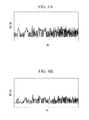
- Figs. 4A and 4B the results of measuring the noise of the control board 21 obtained by providing the capacitance element 29C are shown.
- Fig. 4A which shows a graph before taking the countermeasure
- the noise is reduced to a greater degree over substantially the entire region of a wide frequency band (the amplitude of the noise waveform is smaller over substantially the entire region of the frequency band) in the graph shown in Fig. 4B , obtained after the countermeasure of providing the capacitance element 29C, and it is understood that a considerable noise-reduction effect can be achieved.
- the configuration includes the low-voltage-side ground region 26 that is connected to the frame ground region 28B that is located closest thereto among a plurality of the frame ground regions 28A to 28D through the capacitance element 29D having a capacitance of 0.1 ⁇ F or more. Therefore, it is possible to ground the low-voltage-side ground region 26 to the frame ground region 28B through the capacitance element 29D having a capacitance of 0.1 ⁇ F or more, to reduce the electromagnetic noise in the low-voltage-side ground region 26 by readily pulling down the electromagnetic noise to the frame ground region 28B, and to stabilize the low-voltage circuit in terms of noise. Therefore, it is possible to improve the EMC properties of the control board 21 and to increase reliability.
- the high-voltage-side ground region 27 is connected to at least one of a plurality of the frame ground regions 28A to 28D (in this example, three frame ground regions 28B to 28D) through the capacitance elements 32A to 32C having a capacitance of 10,000 pF or more.
- the capacitance elements 32A to 32C each of which has a capacitance of 10,000 pF or more.
- the control board 21 mentioned above it is possible to reduce the electromagnetic noise output from the inverter device 12 and to improve the electromagnetic noise immunity of the inverter device. Therefore, it is possible to prevent malfunction etc. of the inverter device 12 due to noise interference and to improve the electromagnetic compatibility (EMC) of the inverter device 12 to increase its quality and reliability.
- the integrated-inverter electric compressor 1 is configured by building the inverter device 12 into the inverter accommodating portion 9 of the housing 2, it is possible to reduce the electromagnetic noise output from the inverter device 12 and to improve the electromagnetic noise immunity of the inverter device. Therefore, while preventing malfunction of the inverter device 12 due to noise interference, the electric compressor 1 can be driven stably, and the electromagnetic compatibility (EMC) of the integrated-inverter electric compressor 1 can be improved to increase its quality and reliability.
- the present invention is not limited to the invention according to the above-described embodiments, and appropriate modifications are permissible within a range that does not depart from the spirit thereof.
- the configurations are not limited thereto, and it is needless to say that the present invention can be applied to various types of inverter devices and integrated-inverter electric compressors.
- the inverter device need not necessarily be formed as a module.
- the CAN communication lines 24 are not connected to the low-voltage-side ground region and the frame ground region through the capacitance element, it is also possible to connect the CAN communication lines 24 to the low-voltage-side ground region and the frame ground region through capacitance elements as required. However, because there is a risk that connecting a capacitance element may cause signal distortion, the decision may be made by taking this issue into consideration.
Landscapes
- Engineering & Computer Science (AREA)
- Power Engineering (AREA)
- Microelectronics & Electronic Packaging (AREA)
- Physics & Mathematics (AREA)
- Electromagnetism (AREA)
- Inverter Devices (AREA)
Abstract
Description
- The present invention relates to a control board suitable for an inverter device, to an inverter device using the same, and to an integrated-inverter electric compressor in which the inverter device is integrated.
- Air conditioners installed in electric vehicles, hybrid vehicles, and so forth employ integrated-inverter electric compressors in which inverter devices are integrally built in. These integrated-inverter electric compressors are configured such that an inverter device, which converts DC power supplied from the on-board power to three-phase AC power, is integrally built into a housing of the electric compressor, and the compressor is driven by applying three-phase AC power converted by the inverter device to an electric motor accommodated in the housing.
- Two power systems, a high-voltage power system for rotationally driving the electric motor and a low-voltage power system for control and communication, are connected to the inverter device. A control board used for the inverter device is configured so as to be correspondingly partitioned into a region in which a low-voltage circuit pattern is provided and a region in which a high-voltage circuit pattern is provided and so as to have a respective low-voltage-side ground region and a high-voltage-side ground region formed correspondingly to the circuit regions (for example, see PTLs 1 and 2).
- In addition, because power lines, communication lines, and so forth are connected to the inverter device, electromagnetic noise is radiated from the outside through these lines. Because the inverter device includes high-voltage electronic components, such as semiconductor switching elements etc., the inverter device itself serves as a source of electromagnetic noise. In order to reduce the input/output of such electromagnetic noise, PTL 1 discloses a control board and a control device in which a patterned low-voltage-side ground is directly grounded to the casing (frame), a high-voltage-side ground is grounded to the casing (frame) through a capacitance element, such as a capacitor etc., and the low-voltage-side ground region and the high-voltage-side ground region are connected through the capacitor.
-
- {PTL 1} Japanese Unexamined Patent Application, Publication No.
2008-99480 Fig. 2 ) - {PTL 2} Japanese Unexamined Patent Application, Publication No.
2009-89511 - However, inverter devices have been increasingly reduced in size, and along with this trend, control boards used in inverter modules have also been increasingly reduced in size and increased in density. In addition, other than power lines and ground lines, about six communication-related input/output lines are connected to some inverter modules, and there is a trend towards an increasing number of input/output lines. Therefore, with an inverter device to which two power systems are connected, the generation of noise and transmission routes of electromagnetic noise become more complex, and the noise itself tends to grow; accordingly, it has become difficult to achieve electromagnetic compatibility (EMC; Electro-Magnetic Compatibility) with the configuration disclosed in PTL 1.
- The present invention has been conceived in light of the above-described circumstances, and an object thereof is to provide a control board, an inverter device, and an integrated-inverter electric compressor that are capable of improving electromagnetic compatibility (EMC properties) and of improving reliability against input/output of electromagnetic noise, which is showing a tendency to become more complicated and more intense.
- In order to solve the problems described above, a control board, an inverter device, and an integrated-inverter electric compressor according to the present invention employ the following solutions.
That is, a control board according to a first aspect of the present invention is a control board to which two power systems, a low-voltage power system and a high-voltage power system, are input, comprising a low-voltage circuit and a high-voltage circuit, and a low-voltage-side ground region and a high-voltage-side ground region that are formed in correspondence with the circuits, respectively, wherein frame ground regions are provided at a plurality of positions on the control board, and a plurality of communication line patterns connected to the low-voltage circuit are respectively connected to both the low-voltage-side ground region and the frame ground regions through capacitance elements with various capacitances. - According to the first aspect of the present invention, the frame ground regions are provided at a plurality of positions on the control board, and a plurality of the communication line patterns connected to the low-voltage circuit are respectively connected to both the low-voltage-side ground region and the frame ground regions through the capacitance elements with various capacitances. Therefore, it is possible to stabilize the low-voltage circuit in terms of noise by reducing the electromagnetic noise in various frequency bands that is input/output through a plurality of communication lines by pulling down the electromagnetic noise to the low-voltage-side ground region and the frame ground regions through the capacitance elements having various capacitances. Thus, it is possible to improve the electromagnetic compatibility (EMC; Electro-Magnetic Compatibility) of the control board and to increase the reliability against increasing complexity, intensity, etc. of generated noise and noise transmission routes due to the properties of the control board, size-reduction of the control board, an increase in the number of communication lines, and so forth.
- Furthermore, in the control board according to the first aspect of the present invention, for the above-described control board, the capacitance elements that are connected between the plurality of communication line patterns and the frame ground region may have capacitances of 0.1 µF or more, and the capacitance elements that are connected between the communication line patterns and the low-voltage-side ground region may have capacitances of pF order.
- According to the first aspect of the present invention, the capacitance elements that are connected between the communication line patterns and the frame ground regions have capacitances of 0.1 µF or more, and the capacitance elements that are connected between the communication line patterns and the low-voltage-side ground region have capacitances of pF order. Therefore, the conductive noise is mainly pulled down to the frame ground region through the capacitance elements that have a capacitance of 0.1 µF or more and that are connected to the frame ground regions, and the radiated noise is mainly pulled down to the low-voltage-side ground region through the capacitance elements that have a capacitance of pF order and that are connected to the low-voltage-side ground region; by doing so, the noise can be reduced in a wide frequency band. Therefore, the control board can be made compliant with several noise tests, and it is possible to improve the EMC properties of the control board.
- Furthermore, in the control board according to the first aspect of the present invention, for any of the above-described control boards, the plurality of communication line patterns may be connected to the frame ground region that is located closest to connecting positions of the communication lines through the capacitance elements.
- According to the first aspect of the present invention, the communication line patterns are connected to the frame ground region that is located closest to the connecting positions of the communication lines through the capacitance elements. Therefore, it is possible to pull down the electromagnetic noise to the frame ground region at a location closer to the generation source and to reduce the electromagnetic noise more effectively. Therefore, it is possible to further improve the EMC properties of the control boards.
- Furthermore, in the control board according to the first aspect of the present invention, for any of the above-described control boards, the ground line may be connected to the low-voltage-side ground region, and the ground line is connected to one of the frame ground regions through the capacitance element having a capacitance of 0.1 µF or more.
- According to the first aspect of the present invention, the ground line is connected to the low-voltage-side ground region, and the ground line is connected to one of the frame ground regions through the capacitance element having a capacitance of 0.1 µF or more. Therefore, it is possible to reduce the electromagnetic noise input from and output to the low-voltage-side ground region through the ground line by pulling down the electromagnetic noise to the frame ground regions through the capacitance elements; thereby, it is possible to improve the EMC properties of the control board.
- Furthermore, in the control board according to the first aspect of the present invention, for any of the above-described control boards, the low-voltage-side ground region may be connected to one of the frame ground regions through a capacitance element having a capacitance of 0.1 µF or more.
- According to the first aspect of the present invention, the low-voltage-side ground region is connected to one of the frame ground regions through the capacitance element having a capacitance of 0.1 µF or more. Therefore, it is possible to ground the low-voltage-side ground region to the frame ground region through the capacitance element having a capacitance of 0.1 µF or more, to reduce the electromagnetic noise in the low-voltage-side ground region by pulling down the electromagnetic noise to the frame ground region, and to stabilize the low-voltage circuit in terms of noise. Therefore, it is possible to improve the EMC properties of the control board and to increase the reliability.
- Furthermore, in the control board according to the first aspect of the present invention, for the above-described control board, the low-voltage-side ground region may be connected to the frame ground region that is located closest to that low-voltage-side ground region through one of the capacitance elements.
- According to the configuration of the first aspect of the present invention mentioned above, the low-voltage-side ground region is connected to the frame ground region that is located closest to the low-voltage-side ground region through one of the capacitance elements. Therefore, it is possible to ground the low-voltage-side ground region to the frame ground region that is located closest thereto through the capacitance element having a capacitance of 0.1 µF or more and to reduce the electromagnetic noise in the low-voltage-side ground region by readily pulling down the electromagnetic noise to the frame ground region. Therefore, it is possible to stabilize the low-voltage circuit in terms of noise and to improve the EMC properties of the control board.
- Furthermore, the control board according to the first aspect of the present invention, for any of the above-described control boards, the high-voltage-side ground region may be connected to at least one of the frame ground regions through capacitance elements having a capacitance of 10,000 pF or more.
- According to the first aspect of the present invention, the high-voltage-side ground region is connected to at least one of the frame ground regions through the capacitance elements having a capacitance of 10,000 pF or more. Therefore, it is possible to ground the high-voltage-side ground region to at least one of the plurality of frame ground regions through the capacitance elements having a capacitance of 10,000 pF or more, to reduce the electromagnetic noise entering the high-voltage-side ground region by pulling down the electromagnetic noise to the frame ground region that is located closest thereto, and to stabilize the high-voltage circuit in terms of noise. Therefore, it is possible to improve the EMC properties of the control board and to increase reliability.
- Furthermore, in the control board according to the first aspect of the present invention, for the above-described control board, the high-voltage-side ground region may be connected to the frame ground region that is located closest to that high-voltage-side ground region through the capacitance element.
- According to the configuration of the first aspect of the present invention mentioned above, the high-voltage-side ground region is connected to the frame ground region that is located closest to that high-voltage-side ground region through the capacitance element. Therefore, it is possible to ground the high-voltage-side ground region to the frame ground region that is located closest thereto through the capacitance element having a capacitance of 10,000 pF or more and to reduce the electromagnetic noise entering the high-voltage-side ground region by readily pulling down the electromagnetic noise to the frame ground region. Therefore, it is possible to stabilize the high-voltage circuit in terms of noise and to improve the EMC properties of the control board.
- Furthermore, a control board according to a second aspect of the present invention is a control board to which two power systems, a low-voltage power system and a high-voltage power system, are input, comprising a low-voltage circuit and a high-voltage circuit, and a low-voltage-side ground region and a high-voltage-side ground region that are formed in correspondence with the circuits, respectively, wherein frame ground regions are provided at a plurality of positions on the control board, and the low-voltage-side ground region is connected to one of the frame ground regions through a capacitance element having a capacitance of 0.1 µF or more.
- According to the second aspect of the present invention, the frame ground regions are provided at a plurality of positions on the control board, and the low-voltage-side ground region is connected to one of the frame ground regions through the capacitance element having a capacitance of 0.1 µF or more. Therefore, it is possible to ground the low-voltage-side ground region to the frame ground region through the capacitance element having a capacitance of 0.1 µF or more, to reduce mainly the conductive noise by readily pulling down the electromagnetic noise entering the low-voltage-side ground region to the frame ground region, and to stabilize the low-voltage circuit in terms of noise. Therefore, it is possible to improve the EMC properties of the control board and to increase reliability.
- Furthermore, a control board according to a third aspect of the present invention is a control board to which two power systems, a low-voltage power system and a high-voltage power system, are input, comprising a low-voltage circuit and a high-voltage circuit, and a low-voltage-side ground region and a high-voltage-side ground region that are formed in correspondence with the circuits, respectively, wherein frame ground regions are provided at a plurality of positions on the control board, and the high-voltage-side ground region is connected to at least one of the frame ground regions through a capacitance element having a capacitance of 10,000 pF or more.
- According to the third aspect of the present invention, the frame ground regions are provided at a plurality of locations in the control board, and the high-voltage-side ground region is connected at least one of the frame ground regions through the capacitance element having a capacitance of 10,000 pF or more. Therefore, it is possible to ground the high-voltage-side ground region to at least one of the frame ground regions that are located at a plurality of locations through the capacitance element having a capacitance of 10,000 pF or more, to reduce the electromagnetic noise in the high-voltage-side ground region by readily pulling down the electromagnetic noise to the frame ground region that is located closest thereto, and to stabilize the high-voltage circuit in terms of noise. Therefore, it is possible to improve the EMC properties of the control board and to increase reliability, and at the same time, because the capacitance of the capacitance element connected to the frame ground region is 10,000 pF or more, it is possible to prevent a leakage current flowing towards the frame side.
- Furthermore, an inverter device according to a fourth aspect of the present invention is an inverter device comprising any of the above-described control boards.
- According to the fourth aspect of the present invention, the inverter device is an inverter device including any of the above-described control boards. Therefore, it is possible to reduce the electromagnetic noise output from the inverter device and to improve the electromagnetic noise immunity of the inverter device. Therefore, it is possible to prevent malfunction etc. of the inverter device due to noise interference and to improve the electromagnetic compatibility (EMC) of the inverter device, increasing its quality and reliability.
- Furthermore, an integrated-inverter electric compressor according to a fifth aspect of the present invention is an integrated-inverter electric compressor in which an inverter device comprising any of the above-described control board is integrally built into a housing.
- According to the fifth aspect of the present invention, the integrated-inverter electric compressor is an integrated-inverter electric compressor in which the inverter device including any of the above-described control boards is integrally built into a housing. Therefore, it is possible to reduce the electromagnetic noise output from the inverter device and to improve the electromagnetic noise immunity of the inverter device. Therefore, the electric compressor can be driven stably while preventing malfunction etc. of the inverter device due to the noise interference, and the electromagnetic compatibility (EMC) of the integrated-inverter electric compressor can be improved, increasing its quality and reliability.
- According to the control board of the present invention, it is possible to reduce the electromagnetic noise in various frequency bands that is input/output through a plurality of communication lines by pulling down the electromagnetic noise to the low-voltage-side ground region and the frame ground region through the capacitance element with various capacitances, and to stabilize the low-voltage circuit in terms of noise; therefore, it is possible to improve the electromagnetic compatibility (EMC; Electro-Magnetic Compatibility) of the control board and to increase the reliability against increasing complexity, intensity, etc. of generated noise and noise transmission routes due to the properties of the control board, size-reduction of the control board, an increase in the number of communication lines, and so forth.
- In addition, according to the control board of the present invention, it is possible to ground the low-voltage-side ground region to the frame ground region through the capacitance element having a capacitance of 0.1 µF or more, to reduce mainly conductive noise by readily pulling down the electromagnetic noise entering the low-voltage-side ground region to the frame ground region, and to stabilize the low-voltage circuit in terms of noise; therefore, it is possible to improve the EMC properties of the control board and to increase reliability.
- In addition, according to the control board of the present invention, it is possible to ground the high-voltage-side ground region to at least one of the frame ground regions that are located at a plurality of locations through the capacitance element having a capacitance of 10,000 pF or more, to reduce the electromagnetic noise in the high-voltage-side ground region by readily pulling down the electromagnetic noise to the frame ground region that is located closest thereto, and to stabilize the high-voltage circuit in terms of noise; therefore, it is possible to improve the EMC properties of the control board and to increase reliability.
- In addition, according to the inverter device and the integrated-inverter electric compressor of the present invention, it is possible to reduce the electromagnetic noise that is output from the inverter device and to improve the electromagnetic noise immunity of the inverter device; therefore, it is possible to prevent malfunction etc. of the inverter device due to noise interference, to improve the electromagnetic compatibility (EMC) of the inverter device and the integrated-inverter electric compressor with a built-in inverter device, and to increase the quality and reliability thereof.
-
- {
FIG. 1} FIG. 1 is a side view of an integrated-inverter electric compressor according to one embodiment of the present invention. - {
FIG. 2} FIG. 2 is a perspective view of an inverter device (inverter module) that is integrally built into the integrated-inverter electric compressor ofFig. 1 . - {
FIG. 3} FIG. 3 is a schematic view of a control board used in the inverter device (inverter module) ofFig. 2 . - {
FIG. 4A} FIG. 4A is a graph of measurements before taking a countermeasure exhibiting a noise reduction effect according to the present invention. - {
FIG. 4B} FIG. 4B is a graph of measurements after taking a countermeasure exhibiting a noise reduction effect according to the present invention. - An embodiment of the present invention will be described below with reference to
Figs. 1 to 4B .
A side view of an integrated-inverter electric compressor according to an embodiment of the present invention is shown inFig. 1 , a perspective view of an inverter device (inverter module) that is built in thereto is shown inFig. 2 , and a schematic view of a control board thereof is shown inFig. 3 .
An integrated-inverter electric compressor 1 is provided with ahousing 2 that forms an outer shell. Thehousing 2 is constructed by integrally connecting amotor housing 3 that accommodates an electric motor (not shown) and a compressor housing 4 that accommodates a compressor mechanism (not shown) usingbolts 5. Themotor housing 3 and the compressor housing 4 are pressure-resistant containers formed of die-cast aluminum. - The electric motor and compressor mechanism (not shown) accommodated in the
housing 2 are linked through a motor shaft, and the compressor mechanism is configured so as to be driven by the rotation of the electric motor. Acoolant inlet port 6 is provided on one side (right-hand side inFig. 1 ) of themotor housing 3, and low-temperature, low-pressure coolant gas sucked into themotor housing 3 through thiscoolant inlet port 6 flows around the electric motor along a motor-axis direction L and is then sucked into and compressed by the compressor mechanism. After the high-temperature, highpressure coolant gas that has been compressed by the compressor mechanism is discharged into the compressor housing 4, the coolant gas is discharged to the outside through an outlet port 7 provided on one side (left-hand side inFig. 1 ) of the compressor housing 4. - In the
housing 2, for example,attachment legs Fig. 1 ) of themotor housing 3 and the lower part of one side (left-hand side inFig. 1 ) of the compressor housing 4, and one position at the upper part of the compressor housing 4. The integrated-inverter electric compressor 1 is mounted on a vehicle by fixedly installing theseattachment legs - An
inverter accommodating portion 9 having a predetermined volume at its upper part is integrally formed on the outer periphery of themotor housing 3. This inverteraccommodating portion 9 has a box-shape with an open top and a surrounding wall with a predetermined height, and two power-line guiding openings 10 are provided on the side surface thereof. The top surface of theinverter accommodating portion 9 can be closed tightly by fixing acover member 11 thereto with screws. - An
inverter device 12 that converts DC power supplied through two power lines from an on-board power unit (battery) (not shown) to three-phase AC power and applies the three-phase AC power to the built-in electric motor in themotor housing 3 to drive the electric motor is accommodated and installed in theinverter accommodating portion 9. Theinverter device 12 is provided with an inverter module 13 (seeFig. 2 ), which is configured by forming a power board, a control board, and so forth as an integral module, and a noise-removing filter circuit (not shown) constituted of high-voltage parts, such as a capacitor (smoothing capacitor), an inductor coil, and so forth. - The
inverter module 13 is provided with a rectangularplastic case 14 in which a power board (not shown) made of an aluminum sheet etc. is integrally insert molded to the bottom part. A switching circuit that is constituted of a semiconductor switching element such as an IGBT etc. is mounted on the power board. In addition to the power board,P-N terminals 15 to which the power lines are connected,U-V-W terminals 16 that supply three-phase AC power to the electric motor,earths 17 andearth terminals 18, numerous connectingterminals 19 that connect the power board and acontrol board 21, and so forth are integrally insert molded in theplastic case 14. - The
plastic case 14 has a rectangular shape, and theP-N terminals 15 are provided so as to protrude from the one side along the side surface in which the power-line guiding openings 10 of theinverter accommodating portion 9 are formed, and theU-V-W terminals 16 are provided so as to protrude from the side that is adjacent to this side and close to the compressor housing 4. Fixinglegs 20, which are fixed by screwing them to the bottom surface of theinverter accommodating portion 9 using bolts, are integrally molded on the four corners of theplastic case 14, respectively. Theearth terminal 18 is formed on the fixingleg 20 in such a manner that a bolt can pass therethrough, and theearth terminal 18 is configured such that frame ground of the power board and thecontrol board 21 are casing-grounded to thehousing 2 by fixing theplastic case 14 onto the bottom surface of theinverter accommodating portion 9 using bolts. - The
control board 21 is arranged at the upper part of theplastic case 14 so as to maintain a certain gap with respect to the power board, and thecontrol board 21 is supported by the numerous connectingterminals 19,earths 17, and so forth. Thecontrol board 21 is provided with a low-voltage circuit for communication that operates at low voltage and a high-voltage circuit that controls AC power to be applied to the electric motor. In regions where the low-voltage circuit and the high-voltage circuit are provided, a low-voltage circuit pattern and a high-voltage circuit pattern are formed, and these respective regions are separated from each other by a predetermined insulation distance. - A control and
communication line 25, which includes at least two communication lines 23 (lines for communicating with the vehicle and lines for waking up from sleeve) and fourCAN communication lines 24, is connected to the low-voltage circuit side of the above-describedinverter module 13 by passing through theinverter accommodating portion 9 viagromet 22. DC power is supplied to theP-N terminals 15 with two power lines 33 (seeFig. 3 ) through the noise-removing filter circuit that is constituted of a capacitor (smoothing capacitor), an inductor coil, and so forth. - Furthermore, as shown in
Fig. 3 , a low-voltage-side ground region 26 and a high-voltage-side ground region 27 are formed in thecontrol board 21 corresponding to the low-voltage circuit pattern and the high-voltage circuit pattern.Frame ground regions earth terminals 18 through theearths 17 provided on the four corners of theplastic case 14, are formed at four locations corresponding to the four corners of thecontrol board 21, respectively. - Respective
communication line patterns communication lines 23 are connected, are connected to theframe ground region 28A that is located closest to the connecting positions of thecommunication lines 23 through capacitance elements (capacitors) 29A and 29B, each of which has a capacitance of 0.1 µF or more, and the respectivecommunication line patterns side ground region 26 through capacitance elements (capacitors) 30A and 30B, each of which has a capacitance of pF order (for example, 1 to 100 pF). A pattern 31A of aground line 31 connected to the low-voltage-side ground region 26 is also connected to theframe ground region 28A that is located closest to the connecting positions thereof through a capacitance element (capacitor) 29C having a capacitance of 0.1 µF or more. - On the other hand, the low-voltage-
side ground region 26 is connected to aframe ground region 28B, which is different from theframe ground region 28A to which twocommunication lines 23 are connected, through a capacitance element (capacitor) 29D having a capacitance of 0.1 µF or more. Furthermore, the high-voltage-side ground region 27 is connected to threeframe ground regions reference numeral 33 inFig. 3 indicates a power line. - With the configuration described above, the following advantages and effects can be afforded by this embodiment.
In the above-described integrated-inverter electric compressor 1, DC power supplied to theinverter device 12 from the on-board power unit through apower line 33 is input to a switching circuit on the power board from theP-N terminals 15 of theinverter module 13 via the noise-removing filter circuit, is converted to three-phase AC power having an instructed frequency by the operation of a semiconductor switching element, which is controlled via thecontrol board 21, and is then applied to the electric motor in themotor housing 3 from theU-V-W terminals 16 through a glass-sealed terminal (not shown). - As a result, the electric motor is rotationally driven at the instructed frequency to drive the compressor mechanism, thereby performing compression of the coolant. The
inverter device 12 is controlled on the basis of an instruction input from an on-board ECU through the control andcommunication line 25, and the controlled state thereof is fed back to the on-board ECU. Because theinverter device 12 that is built into thehousing 2 of the electric compressor 1 is connected to an external unit through thepower line 33 and a plurality of control andcommunication lines 25, these lines serve as antennas to allow electromagnetic noise to be radiated from the outside. On the other hand, because a high-voltage electronic component, such as an IGBT etc., that performs a switching operation is built into theinverter device 12, theinverter device 12 itself serves as a radiation source for radiating electromagnetic noise. - Nevertheless, in this embodiment, in the
control board 21 in which low-voltage circuits and high-voltage circuits are provided, because the low-voltage-side ground region 26 and the high-voltage-side ground region 27 are formed in correspondence with the respective circuits, and theframe ground regions 28A to 28D are provided on four locations at each corner of thecontrol board 21, respectively, a plurality ofcommunication line patterns side ground region 26 and theframe ground region 28A through thecapacitance elements - Therefore, it is possible to stabilize the low-voltage circuit in terms of noise by reducing the electromagnetic noise in various frequency bands that is input/output through the plurality of
communication lines 23 by pulling down the electromagnetic noise to the low-voltage-side ground region 26 and theframe ground region 28A through thecapacitance elements control board 21 and to increase the reliability against increasing complexity, intensity, etc. of generated noise and noise transmission routes due to the properties of thecontrol board 21, size-reduction of thecontrol board 21, an increase in the number ofcommunication lines 23, and so forth. - Specifically, the capacitances of the
capacitance elements communication line patterns frame ground region 28A are set to 0.1 µF or more, and the capacitances of thecapacitance elements communication line patterns side ground region 26 are set to be on the order of pF (1 to 100 pF). Therefore, the conductive noise is mainly pulled down to theframe ground region 28A through thecapacitance elements frame ground region 28A, and the radiated noise is mainly pulled down to the low-voltage-side ground region 26 through thecapacitance elements side ground region 26; thereby, noise can be reduced in a wide frequency band. Therefore, thecontrol board 21 can be made compliant with several noise tests, and it is possible to improve the EMC properties of thecontrol board 21. - In this embodiment, because the
communication line patterns frame ground region 28A that is located closest to the connecting positions of thecommunication lines 23 through thecapacitance elements frame ground region 28A at a location closer to the generation source and to reduce the electromagnetic noise more effectively. Therefore, it is possible to further improve the EMC properties of thecontrol board 21. - The
ground line 31, which is connected to the low-voltage-side ground region 26, is connected to theframe ground region 28A, which is one of a plurality of theframe ground regions 28A to 28D, through thecapacitance element 29C having a capacitance of 0.1 µF or more. Therefore, it is possible to reduce the electromagnetic noise that is input/output through theground line 31 connected to the low-voltage-side ground region 26 by pulling down the electromagnetic noise to theframe ground region 28A through thecapacitance element 29C, thereby improving the EMC properties of thecontrol board 21. - In
Figs. 4A and 4B , the results of measuring the noise of thecontrol board 21 obtained by providing thecapacitance element 29C are shown. In comparison withFig. 4A , which shows a graph before taking the countermeasure, it can be seen that the noise is reduced to a greater degree over substantially the entire region of a wide frequency band (the amplitude of the noise waveform is smaller over substantially the entire region of the frequency band) in the graph shown inFig. 4B , obtained after the countermeasure of providing thecapacitance element 29C, and it is understood that a considerable noise-reduction effect can be achieved. - In this embodiment, the configuration includes the low-voltage-
side ground region 26 that is connected to theframe ground region 28B that is located closest thereto among a plurality of theframe ground regions 28A to 28D through thecapacitance element 29D having a capacitance of 0.1 µF or more. Therefore, it is possible to ground the low-voltage-side ground region 26 to theframe ground region 28B through thecapacitance element 29D having a capacitance of 0.1 µF or more, to reduce the electromagnetic noise in the low-voltage-side ground region 26 by readily pulling down the electromagnetic noise to theframe ground region 28B, and to stabilize the low-voltage circuit in terms of noise. Therefore, it is possible to improve the EMC properties of thecontrol board 21 and to increase reliability. - Furthermore, in this embodiment, the high-voltage-
side ground region 27 is connected to at least one of a plurality of theframe ground regions 28A to 28D (in this example, threeframe ground regions 28B to 28D) through thecapacitance elements 32A to 32C having a capacitance of 10,000 pF or more. Thus, it is possible to ground the high-voltage-side ground region 27 to at least one of the plurality offrame ground regions 28A to 28D through thecapacitance elements 32A to 32C, each of which has a capacitance of 10,000 pF or more. - Therefore, it is possible to stabilize the high-voltage circuit in terms of noise by reducing the electromagnetic noise in the high-voltage-
side ground region 27 by pulling down the electromagnetic noise to one of theframe ground regions 28B to 28D that is located closest thereto; by doing so, it is also possible to improve the EMC properties of thecontrol board 21 and to increase reliability. - By employing the
control board 21 mentioned above, it is possible to reduce the electromagnetic noise output from theinverter device 12 and to improve the electromagnetic noise immunity of the inverter device. Therefore, it is possible to prevent malfunction etc. of theinverter device 12 due to noise interference and to improve the electromagnetic compatibility (EMC) of theinverter device 12 to increase its quality and reliability. Similarly, because the integrated-inverter electric compressor 1 is configured by building theinverter device 12 into theinverter accommodating portion 9 of thehousing 2, it is possible to reduce the electromagnetic noise output from theinverter device 12 and to improve the electromagnetic noise immunity of the inverter device. Therefore, while preventing malfunction of theinverter device 12 due to noise interference, the electric compressor 1 can be driven stably, and the electromagnetic compatibility (EMC) of the integrated-inverter electric compressor 1 can be improved to increase its quality and reliability. - The present invention is not limited to the invention according to the above-described embodiments, and appropriate modifications are permissible within a range that does not depart from the spirit thereof. For example, although example configurations of the
inverter device 12 and the integrated-inverter electric compressor 1 into which theinverter device 12 is integrated are shown in the above-described embodiment, the configurations are not limited thereto, and it is needless to say that the present invention can be applied to various types of inverter devices and integrated-inverter electric compressors. In addition, the inverter device need not necessarily be formed as a module. - Furthermore, in the above-described embodiment, although the
CAN communication lines 24 are not connected to the low-voltage-side ground region and the frame ground region through the capacitance element, it is also possible to connect theCAN communication lines 24 to the low-voltage-side ground region and the frame ground region through capacitance elements as required. However, because there is a risk that connecting a capacitance element may cause signal distortion, the decision may be made by taking this issue into consideration. -
- 1 integrated-inverter electric compressor
- 2 housing
- 9 inverter accommodating portion
- 12 inverter device
- 13 inverter module
- 21 control board
- 23 communication line
- 23A, 23B communication line pattern
- 24 CAN communication line
- 25 control and communication line
- 26 low-voltage-side ground region
- 27 high-voltage-side ground region
- 28A, 28B, 28C, 28D frame ground region
- 29A, 29B, 29C, 29D capacitance element (capacitance is 0.1 µF or more)
- 30A, 30B capacitance element (capacitance is pF order)
- 31 ground line
- 32A, 32B, 32C capacitance element (capacitance is 10,000 pF or more)
- 33 power line
Claims (12)
- A control board to which two power systems, a low-voltage power system and a high-voltage power system, are input, comprising a low-voltage circuit and a high-voltage circuit, and a low-voltage-side ground region and a high-voltage-side ground region that are formed in correspondence with the circuits, respectively,
wherein frame ground regions are provided at a plurality of positions on the control board, and
a plurality of communication line patterns connected to the low-voltage circuit are respectively connected to both the low-voltage-side ground region and the frame ground regions through capacitance elements with various capacitances. - A control board according to Claim 1, wherein the capacitance elements that are connected between the plurality of communication line patterns and the frame ground region have capacitances of 0.1 µF or more, and the capacitance elements that are connected between the communication line patterns and the low-voltage-side ground region have capacitances of pF order.
- A control board according to Claim 1 or 2, wherein the plurality of the communication line patterns are connected to the frame ground region that is located closest to connecting positions of the communication lines through the capacitance elements.
- A control board according to any one of Claims 1 to 3, wherein a ground line is connected to the low-voltage-side ground region, and the ground line is connected to one of the frame ground regions through a capacitance element having a capacitance of 0.1 µF or more.
- A control board according to any one of Claims 1 to 4, wherein the low-voltage-side ground region is connected to one of the frame ground regions through a capacitance element having a capacitance of 0.1 µF or more.
- A control board according to Claim 5, wherein the low-voltage-side ground region is connected to the frame ground region that is located closest to that low-voltage-side ground region through one of the capacitance elements.
- A control board according to any one of Claims 1 to 6, wherein the high-voltage-side ground region is connected to at least one of the frame ground regions through capacitance elements having a capacitance of 10,000 pF or more.
- A control board according to Claim 7, wherein the high-voltage-side ground region is connected to the frame ground region that is located closest to that high-voltage-side ground region through the capacitance element.
- A control board to which two power systems, a low-voltage power system and a high-voltage power system, are input, comprising a low-voltage circuit and a high-voltage circuit, and a low-voltage-side ground region and a high-voltage-side ground region that are formed in correspondence with the circuits, respectively,
wherein frame ground regions are provided at a plurality of positions on the control board, and
the low-voltage-side ground region is connected to one of the frame ground regions through a capacitance element having a capacitance of 0.1 µF or more. - A control board to which two power systems, a low-voltage power system and a high-voltage power system, are input, comprising a low-voltage circuit and a high-voltage circuit, and a low-voltage-side ground region and a high-voltage-side ground region that are formed in correspondence with the circuits, respectively,
wherein frame ground regions are provided at a plurality of positions on the control board, and
the high-voltage-side ground region is connected to at least one of the frame ground regions through a capacitance element having a capacitance of 10,000 pF or more. - An inverter device comprising the control board according to any one of Claims 1 to 10.
- An integrated-inverter electric compressor in which an inverter device comprising the control board according to any one of Claims 1 to 10 is integrally built into a housing.
Applications Claiming Priority (2)
| Application Number | Priority Date | Filing Date | Title |
|---|---|---|---|
| JP2009296158A JP5448797B2 (en) | 2009-12-25 | 2009-12-25 | Control board, inverter device, and inverter-integrated electric compressor |
| PCT/JP2010/072904 WO2011078123A1 (en) | 2009-12-25 | 2010-12-20 | Control circuit board, inverter device, and inverter integrated motor-driven compressor |
Publications (3)
| Publication Number | Publication Date |
|---|---|
| EP2518887A1 true EP2518887A1 (en) | 2012-10-31 |
| EP2518887A4 EP2518887A4 (en) | 2017-09-20 |
| EP2518887B1 EP2518887B1 (en) | 2018-10-31 |
Family
ID=44195649
Family Applications (1)
| Application Number | Title | Priority Date | Filing Date |
|---|---|---|---|
| EP10839353.9A Active EP2518887B1 (en) | 2009-12-25 | 2010-12-20 | Control circuit board, inverter device, and inverter integrated motor-driven compressor |
Country Status (4)
| Country | Link |
|---|---|
| US (1) | US8952766B2 (en) |
| EP (1) | EP2518887B1 (en) |
| JP (1) | JP5448797B2 (en) |
| WO (1) | WO2011078123A1 (en) |
Families Citing this family (11)
| Publication number | Priority date | Publication date | Assignee | Title |
|---|---|---|---|---|
| JP5308917B2 (en) * | 2009-05-29 | 2013-10-09 | サンデン株式会社 | Inverter-integrated electric compressor |
| JP5733945B2 (en) * | 2010-10-15 | 2015-06-10 | 三菱重工業株式会社 | Inverter module and inverter-integrated electric compressor |
| WO2014058843A2 (en) * | 2012-10-08 | 2014-04-17 | Trane International Inc. | Hvac electrical system power supply packaging system |
| JP5893082B2 (en) * | 2014-06-18 | 2016-03-23 | 三菱電機株式会社 | Power converter |
| KR20160011867A (en) * | 2014-07-23 | 2016-02-02 | 엘에스산전 주식회사 | Inverter assembly without galvanic isolation |
| CN105101770A (en) * | 2015-09-14 | 2015-11-25 | 南京金龙新能源汽车研究院有限公司 | Anti-electromagnetic interference system for electric car compressor |
| CN105743286A (en) * | 2016-03-02 | 2016-07-06 | 广州佳林医疗科技有限公司 | Electromagnetic compatibility (EMC) device of flusher |
| JP7247748B2 (en) * | 2019-05-24 | 2023-03-29 | 株式会社デンソー | power converter |
| JP6745386B1 (en) * | 2019-06-21 | 2020-08-26 | 株式会社ケーヒン | Power converter |
| WO2021106941A1 (en) * | 2019-11-25 | 2021-06-03 | アイシン・エィ・ダブリュ株式会社 | Control substrate |
| DE102021205645A1 (en) | 2021-06-02 | 2022-12-08 | Volkswagen Aktiengesellschaft | Thermal management control module with integrated control |
Family Cites Families (13)
| Publication number | Priority date | Publication date | Assignee | Title |
|---|---|---|---|---|
| US4356480A (en) * | 1980-09-11 | 1982-10-26 | Minnesota Mining And Manufacturing Company | Liquid level sensing circuitry |
| JP3033424B2 (en) * | 1994-02-28 | 2000-04-17 | 松下電工株式会社 | Balance-unbalance converter |
| DE19516918A1 (en) * | 1995-05-09 | 1996-11-14 | Bosch Gmbh Robert | Control device, in particular for controlling functions of a motor vehicle |
| JPH08322264A (en) * | 1995-05-25 | 1996-12-03 | Sanden Corp | Inverter |
| US6023202A (en) * | 1998-02-13 | 2000-02-08 | Hewlett-Packard Company | Ground return for high speed digital signals that are capacitively coupled across a DC-isolated interface |
| US6735968B2 (en) | 2002-03-29 | 2004-05-18 | Hitachi, Ltd. | Refrigerating apparatus and an inverter device used therein |
| JP3682550B2 (en) * | 2002-03-29 | 2005-08-10 | 株式会社日立製作所 | Refrigeration apparatus and inverter apparatus used therefor |
| US7292449B2 (en) * | 2004-12-13 | 2007-11-06 | Lexmark International, Inc. | Virtual ground return for reduction of radiated emissions |
| JP5039356B2 (en) * | 2006-10-13 | 2012-10-03 | 三菱重工業株式会社 | Control board, control device for electric compressor, and electric compressor |
| JP5173344B2 (en) | 2007-09-28 | 2013-04-03 | 三菱重工業株式会社 | Electric compressor for in-vehicle air conditioner |
| JP2009146962A (en) * | 2007-12-12 | 2009-07-02 | Panasonic Corp | Noise reduction circuit |
| JP5199698B2 (en) | 2008-02-28 | 2013-05-15 | 三菱重工業株式会社 | Integrated electric compressor |
| JP4735670B2 (en) * | 2008-06-11 | 2011-07-27 | 富士ゼロックス株式会社 | Printed circuit board and image processing apparatus |
-
2009
- 2009-12-25 JP JP2009296158A patent/JP5448797B2/en active Active
-
2010
- 2010-12-20 WO PCT/JP2010/072904 patent/WO2011078123A1/en not_active Ceased
- 2010-12-20 EP EP10839353.9A patent/EP2518887B1/en active Active
- 2010-12-20 US US13/386,287 patent/US8952766B2/en active Active
Non-Patent Citations (1)
| Title |
|---|
| See references of WO2011078123A1 * |
Also Published As
| Publication number | Publication date |
|---|---|
| US20120119688A1 (en) | 2012-05-17 |
| EP2518887B1 (en) | 2018-10-31 |
| JP2011139551A (en) | 2011-07-14 |
| US8952766B2 (en) | 2015-02-10 |
| WO2011078123A1 (en) | 2011-06-30 |
| EP2518887A4 (en) | 2017-09-20 |
| JP5448797B2 (en) | 2014-03-19 |
Similar Documents
| Publication | Publication Date | Title |
|---|---|---|
| EP2518887B1 (en) | Control circuit board, inverter device, and inverter integrated motor-driven compressor | |
| US9115707B2 (en) | Inverter module and integrated-inverter electric compressor using the same | |
| JP5107114B2 (en) | Inverter-integrated electric compressor | |
| EP2194634B1 (en) | Electric compressor for on-vehicle air conditioner | |
| EP2206922B1 (en) | Inverter-integrated electric compressor | |
| JP6195453B2 (en) | Inverter-integrated electric compressor | |
| JP6180810B2 (en) | Inverter-integrated electric compressor | |
| US20100181876A1 (en) | Inverter-integrated electric compressor | |
| EP2680427A1 (en) | Inverter integrated motor-driven compressor | |
| JP2011069247A (en) | Inverter integrated motor-driven compressor | |
| US9722474B2 (en) | Inverter-integrated electric compressor | |
| CN108369863B (en) | Power conversion device | |
| US9735644B2 (en) | Inverter-integrated electric compressor | |
| JP5595461B2 (en) | Inverter-integrated electric compressor | |
| JP5536172B2 (en) | Inverter-integrated electric compressor | |
| WO2024135248A1 (en) | On-vehicle electric compressor |
Legal Events
| Date | Code | Title | Description |
|---|---|---|---|
| PUAI | Public reference made under article 153(3) epc to a published international application that has entered the european phase |
Free format text: ORIGINAL CODE: 0009012 |
|
| 17P | Request for examination filed |
Effective date: 20120124 |
|
| AK | Designated contracting states |
Kind code of ref document: A1 Designated state(s): AL AT BE BG CH CY CZ DE DK EE ES FI FR GB GR HR HU IE IS IT LI LT LU LV MC MK MT NL NO PL PT RO RS SE SI SK SM TR |
|
| DAX | Request for extension of the european patent (deleted) | ||
| RA4 | Supplementary search report drawn up and despatched (corrected) |
Effective date: 20170823 |
|
| RIC1 | Information provided on ipc code assigned before grant |
Ipc: H05K 1/02 20060101ALI20170817BHEP Ipc: H02M 1/44 20070101ALI20170817BHEP Ipc: H02M 7/00 20060101ALI20170817BHEP Ipc: H02M 7/48 20070101AFI20170817BHEP |
|
| GRAP | Despatch of communication of intention to grant a patent |
Free format text: ORIGINAL CODE: EPIDOSNIGR1 |
|
| INTG | Intention to grant announced |
Effective date: 20180711 |
|
| GRAS | Grant fee paid |
Free format text: ORIGINAL CODE: EPIDOSNIGR3 |
|
| GRAA | (expected) grant |
Free format text: ORIGINAL CODE: 0009210 |
|
| AK | Designated contracting states |
Kind code of ref document: B1 Designated state(s): AL AT BE BG CH CY CZ DE DK EE ES FI FR GB GR HR HU IE IS IT LI LT LU LV MC MK MT NL NO PL PT RO RS SE SI SK SM TR |
|
| REG | Reference to a national code |
Ref country code: CH Ref legal event code: EP Ref country code: GB Ref legal event code: FG4D |
|
| REG | Reference to a national code |
Ref country code: AT Ref legal event code: REF Ref document number: 1060587 Country of ref document: AT Kind code of ref document: T Effective date: 20181115 |
|
| REG | Reference to a national code |
Ref country code: DE Ref legal event code: R096 Ref document number: 602010054842 Country of ref document: DE |
|
| REG | Reference to a national code |
Ref country code: IE Ref legal event code: FG4D |
|
| REG | Reference to a national code |
Ref country code: NL Ref legal event code: MP Effective date: 20181031 |
|
| REG | Reference to a national code |
Ref country code: LT Ref legal event code: MG4D |
|
| REG | Reference to a national code |
Ref country code: AT Ref legal event code: MK05 Ref document number: 1060587 Country of ref document: AT Kind code of ref document: T Effective date: 20181031 |
|
| PG25 | Lapsed in a contracting state [announced via postgrant information from national office to epo] |
Ref country code: NO Free format text: LAPSE BECAUSE OF FAILURE TO SUBMIT A TRANSLATION OF THE DESCRIPTION OR TO PAY THE FEE WITHIN THE PRESCRIBED TIME-LIMIT Effective date: 20190131 Ref country code: LT Free format text: LAPSE BECAUSE OF FAILURE TO SUBMIT A TRANSLATION OF THE DESCRIPTION OR TO PAY THE FEE WITHIN THE PRESCRIBED TIME-LIMIT Effective date: 20181031 Ref country code: HR Free format text: LAPSE BECAUSE OF FAILURE TO SUBMIT A TRANSLATION OF THE DESCRIPTION OR TO PAY THE FEE WITHIN THE PRESCRIBED TIME-LIMIT Effective date: 20181031 Ref country code: PL Free format text: LAPSE BECAUSE OF FAILURE TO SUBMIT A TRANSLATION OF THE DESCRIPTION OR TO PAY THE FEE WITHIN THE PRESCRIBED TIME-LIMIT Effective date: 20181031 Ref country code: AT Free format text: LAPSE BECAUSE OF FAILURE TO SUBMIT A TRANSLATION OF THE DESCRIPTION OR TO PAY THE FEE WITHIN THE PRESCRIBED TIME-LIMIT Effective date: 20181031 Ref country code: LV Free format text: LAPSE BECAUSE OF FAILURE TO SUBMIT A TRANSLATION OF THE DESCRIPTION OR TO PAY THE FEE WITHIN THE PRESCRIBED TIME-LIMIT Effective date: 20181031 Ref country code: BG Free format text: LAPSE BECAUSE OF FAILURE TO SUBMIT A TRANSLATION OF THE DESCRIPTION OR TO PAY THE FEE WITHIN THE PRESCRIBED TIME-LIMIT Effective date: 20190131 Ref country code: ES Free format text: LAPSE BECAUSE OF FAILURE TO SUBMIT A TRANSLATION OF THE DESCRIPTION OR TO PAY THE FEE WITHIN THE PRESCRIBED TIME-LIMIT Effective date: 20181031 Ref country code: IS Free format text: LAPSE BECAUSE OF FAILURE TO SUBMIT A TRANSLATION OF THE DESCRIPTION OR TO PAY THE FEE WITHIN THE PRESCRIBED TIME-LIMIT Effective date: 20190228 Ref country code: FI Free format text: LAPSE BECAUSE OF FAILURE TO SUBMIT A TRANSLATION OF THE DESCRIPTION OR TO PAY THE FEE WITHIN THE PRESCRIBED TIME-LIMIT Effective date: 20181031 |
|
| PG25 | Lapsed in a contracting state [announced via postgrant information from national office to epo] |
Ref country code: PT Free format text: LAPSE BECAUSE OF FAILURE TO SUBMIT A TRANSLATION OF THE DESCRIPTION OR TO PAY THE FEE WITHIN THE PRESCRIBED TIME-LIMIT Effective date: 20190301 Ref country code: GR Free format text: LAPSE BECAUSE OF FAILURE TO SUBMIT A TRANSLATION OF THE DESCRIPTION OR TO PAY THE FEE WITHIN THE PRESCRIBED TIME-LIMIT Effective date: 20190201 Ref country code: RS Free format text: LAPSE BECAUSE OF FAILURE TO SUBMIT A TRANSLATION OF THE DESCRIPTION OR TO PAY THE FEE WITHIN THE PRESCRIBED TIME-LIMIT Effective date: 20181031 Ref country code: AL Free format text: LAPSE BECAUSE OF FAILURE TO SUBMIT A TRANSLATION OF THE DESCRIPTION OR TO PAY THE FEE WITHIN THE PRESCRIBED TIME-LIMIT Effective date: 20181031 Ref country code: SE Free format text: LAPSE BECAUSE OF FAILURE TO SUBMIT A TRANSLATION OF THE DESCRIPTION OR TO PAY THE FEE WITHIN THE PRESCRIBED TIME-LIMIT Effective date: 20181031 Ref country code: NL Free format text: LAPSE BECAUSE OF FAILURE TO SUBMIT A TRANSLATION OF THE DESCRIPTION OR TO PAY THE FEE WITHIN THE PRESCRIBED TIME-LIMIT Effective date: 20181031 |
|
| PG25 | Lapsed in a contracting state [announced via postgrant information from national office to epo] |
Ref country code: IT Free format text: LAPSE BECAUSE OF FAILURE TO SUBMIT A TRANSLATION OF THE DESCRIPTION OR TO PAY THE FEE WITHIN THE PRESCRIBED TIME-LIMIT Effective date: 20181031 Ref country code: DK Free format text: LAPSE BECAUSE OF FAILURE TO SUBMIT A TRANSLATION OF THE DESCRIPTION OR TO PAY THE FEE WITHIN THE PRESCRIBED TIME-LIMIT Effective date: 20181031 Ref country code: CZ Free format text: LAPSE BECAUSE OF FAILURE TO SUBMIT A TRANSLATION OF THE DESCRIPTION OR TO PAY THE FEE WITHIN THE PRESCRIBED TIME-LIMIT Effective date: 20181031 |
|
| REG | Reference to a national code |
Ref country code: CH Ref legal event code: PL |
|
| REG | Reference to a national code |
Ref country code: DE Ref legal event code: R097 Ref document number: 602010054842 Country of ref document: DE |
|
| PG25 | Lapsed in a contracting state [announced via postgrant information from national office to epo] |
Ref country code: MC Free format text: LAPSE BECAUSE OF FAILURE TO SUBMIT A TRANSLATION OF THE DESCRIPTION OR TO PAY THE FEE WITHIN THE PRESCRIBED TIME-LIMIT Effective date: 20181031 Ref country code: LU Free format text: LAPSE BECAUSE OF NON-PAYMENT OF DUE FEES Effective date: 20181220 Ref country code: SM Free format text: LAPSE BECAUSE OF FAILURE TO SUBMIT A TRANSLATION OF THE DESCRIPTION OR TO PAY THE FEE WITHIN THE PRESCRIBED TIME-LIMIT Effective date: 20181031 Ref country code: RO Free format text: LAPSE BECAUSE OF FAILURE TO SUBMIT A TRANSLATION OF THE DESCRIPTION OR TO PAY THE FEE WITHIN THE PRESCRIBED TIME-LIMIT Effective date: 20181031 Ref country code: SK Free format text: LAPSE BECAUSE OF FAILURE TO SUBMIT A TRANSLATION OF THE DESCRIPTION OR TO PAY THE FEE WITHIN THE PRESCRIBED TIME-LIMIT Effective date: 20181031 Ref country code: EE Free format text: LAPSE BECAUSE OF FAILURE TO SUBMIT A TRANSLATION OF THE DESCRIPTION OR TO PAY THE FEE WITHIN THE PRESCRIBED TIME-LIMIT Effective date: 20181031 |
|
| PLBE | No opposition filed within time limit |
Free format text: ORIGINAL CODE: 0009261 |
|
| STAA | Information on the status of an ep patent application or granted ep patent |
Free format text: STATUS: NO OPPOSITION FILED WITHIN TIME LIMIT |
|
| REG | Reference to a national code |
Ref country code: IE Ref legal event code: MM4A |
|
| GBPC | Gb: european patent ceased through non-payment of renewal fee |
Effective date: 20190131 |
|
| 26N | No opposition filed |
Effective date: 20190801 |
|
| REG | Reference to a national code |
Ref country code: BE Ref legal event code: MM Effective date: 20181231 |
|
| PG25 | Lapsed in a contracting state [announced via postgrant information from national office to epo] |
Ref country code: FR Free format text: LAPSE BECAUSE OF NON-PAYMENT OF DUE FEES Effective date: 20181231 Ref country code: IE Free format text: LAPSE BECAUSE OF NON-PAYMENT OF DUE FEES Effective date: 20181220 Ref country code: SI Free format text: LAPSE BECAUSE OF FAILURE TO SUBMIT A TRANSLATION OF THE DESCRIPTION OR TO PAY THE FEE WITHIN THE PRESCRIBED TIME-LIMIT Effective date: 20181031 |
|
| PG25 | Lapsed in a contracting state [announced via postgrant information from national office to epo] |
Ref country code: BE Free format text: LAPSE BECAUSE OF NON-PAYMENT OF DUE FEES Effective date: 20181231 |
|
| PG25 | Lapsed in a contracting state [announced via postgrant information from national office to epo] |
Ref country code: CH Free format text: LAPSE BECAUSE OF NON-PAYMENT OF DUE FEES Effective date: 20181231 Ref country code: LI Free format text: LAPSE BECAUSE OF NON-PAYMENT OF DUE FEES Effective date: 20181231 Ref country code: GB Free format text: LAPSE BECAUSE OF NON-PAYMENT OF DUE FEES Effective date: 20190131 |
|
| PG25 | Lapsed in a contracting state [announced via postgrant information from national office to epo] |
Ref country code: MT Free format text: LAPSE BECAUSE OF NON-PAYMENT OF DUE FEES Effective date: 20181220 |
|
| PG25 | Lapsed in a contracting state [announced via postgrant information from national office to epo] |
Ref country code: TR Free format text: LAPSE BECAUSE OF FAILURE TO SUBMIT A TRANSLATION OF THE DESCRIPTION OR TO PAY THE FEE WITHIN THE PRESCRIBED TIME-LIMIT Effective date: 20181031 |
|
| PG25 | Lapsed in a contracting state [announced via postgrant information from national office to epo] |
Ref country code: CY Free format text: LAPSE BECAUSE OF FAILURE TO SUBMIT A TRANSLATION OF THE DESCRIPTION OR TO PAY THE FEE WITHIN THE PRESCRIBED TIME-LIMIT Effective date: 20181031 Ref country code: HU Free format text: LAPSE BECAUSE OF FAILURE TO SUBMIT A TRANSLATION OF THE DESCRIPTION OR TO PAY THE FEE WITHIN THE PRESCRIBED TIME-LIMIT; INVALID AB INITIO Effective date: 20101220 Ref country code: MK Free format text: LAPSE BECAUSE OF NON-PAYMENT OF DUE FEES Effective date: 20181031 |
|
| PGFP | Annual fee paid to national office [announced via postgrant information from national office to epo] |
Ref country code: DE Payment date: 20251028 Year of fee payment: 16 |