EP2518876A1 - High-voltage power supply - Google Patents
High-voltage power supply Download PDFInfo
- Publication number
- EP2518876A1 EP2518876A1 EP09852598A EP09852598A EP2518876A1 EP 2518876 A1 EP2518876 A1 EP 2518876A1 EP 09852598 A EP09852598 A EP 09852598A EP 09852598 A EP09852598 A EP 09852598A EP 2518876 A1 EP2518876 A1 EP 2518876A1
- Authority
- EP
- European Patent Office
- Prior art keywords
- voltage
- power supply
- unit
- output
- circuit
- Prior art date
- Legal status (The legal status is an assumption and is not a legal conclusion. Google has not performed a legal analysis and makes no representation as to the accuracy of the status listed.)
- Granted
Links
Images





Classifications
-
- H—ELECTRICITY
- H02—GENERATION; CONVERSION OR DISTRIBUTION OF ELECTRIC POWER
- H02M—APPARATUS FOR CONVERSION BETWEEN AC AND AC, BETWEEN AC AND DC, OR BETWEEN DC AND DC, AND FOR USE WITH MAINS OR SIMILAR POWER SUPPLY SYSTEMS; CONVERSION OF DC OR AC INPUT POWER INTO SURGE OUTPUT POWER; CONTROL OR REGULATION THEREOF
- H02M7/00—Conversion of AC power input into DC power output; Conversion of DC power input into AC power output
- H02M7/02—Conversion of AC power input into DC power output without possibility of reversal
- H02M7/04—Conversion of AC power input into DC power output without possibility of reversal by static converters
- H02M7/06—Conversion of AC power input into DC power output without possibility of reversal by static converters using discharge tubes without control electrode or semiconductor devices without control electrode
- H02M7/10—Conversion of AC power input into DC power output without possibility of reversal by static converters using discharge tubes without control electrode or semiconductor devices without control electrode arranged for operation in series, e.g. for multiplication of voltage
- H02M7/103—Containing passive elements (capacitively coupled) which are ordered in cascade on one source
-
- H—ELECTRICITY
- H02—GENERATION; CONVERSION OR DISTRIBUTION OF ELECTRIC POWER
- H02M—APPARATUS FOR CONVERSION BETWEEN AC AND AC, BETWEEN AC AND DC, OR BETWEEN DC AND DC, AND FOR USE WITH MAINS OR SIMILAR POWER SUPPLY SYSTEMS; CONVERSION OF DC OR AC INPUT POWER INTO SURGE OUTPUT POWER; CONTROL OR REGULATION THEREOF
- H02M3/00—Conversion of DC power input into DC power output
- H02M3/02—Conversion of DC power input into DC power output without intermediate conversion into AC
- H02M3/04—Conversion of DC power input into DC power output without intermediate conversion into AC by static converters
- H02M3/06—Conversion of DC power input into DC power output without intermediate conversion into AC by static converters using resistors or capacitors, e.g. potential divider
- H02M3/07—Conversion of DC power input into DC power output without intermediate conversion into AC by static converters using resistors or capacitors, e.g. potential divider using capacitors charged and discharged alternately by semiconductor devices with control electrode, e.g. charge pumps
-
- H—ELECTRICITY
- H02—GENERATION; CONVERSION OR DISTRIBUTION OF ELECTRIC POWER
- H02M—APPARATUS FOR CONVERSION BETWEEN AC AND AC, BETWEEN AC AND DC, OR BETWEEN DC AND DC, AND FOR USE WITH MAINS OR SIMILAR POWER SUPPLY SYSTEMS; CONVERSION OF DC OR AC INPUT POWER INTO SURGE OUTPUT POWER; CONTROL OR REGULATION THEREOF
- H02M3/00—Conversion of DC power input into DC power output
- H02M3/02—Conversion of DC power input into DC power output without intermediate conversion into AC
- H02M3/04—Conversion of DC power input into DC power output without intermediate conversion into AC by static converters
- H02M3/10—Conversion of DC power input into DC power output without intermediate conversion into AC by static converters using discharge tubes with control electrode or semiconductor devices with control electrode
- H02M3/145—Conversion of DC power input into DC power output without intermediate conversion into AC by static converters using discharge tubes with control electrode or semiconductor devices with control electrode using devices of a triode or transistor type requiring continuous application of a control signal
- H02M3/155—Conversion of DC power input into DC power output without intermediate conversion into AC by static converters using discharge tubes with control electrode or semiconductor devices with control electrode using devices of a triode or transistor type requiring continuous application of a control signal using semiconductor devices only
Definitions
- the present invention relates to a high voltage power supply that generates a high voltage.
- an electrophotographic image formation apparatus includes a charging roller for charging the surface of a photoconductor drum serving as an image bearing member and a developer roller for developing an electrostatic latent image, which is formed on the photoconductor drum, by using toner serving as a developer.
- a high voltage of about a few hundred V to a few KV (a direct-current high voltage) needs to be applied to this charging roller and this developer roller in order to charge the photoconductor drum and perform development.
- a power supply for high-voltage generation using a wire-wound electromagnetic transformer hereinafter referred to as a high voltage power supply
- a high voltage power supply using an electromagnetic transformer is described in PTL 1, and a desired high voltage can be output to a load.
- PTL 2 discloses the structure for outputting a voltage that an LC resonant circuit obtains by amplifying a voltage (24 V) from a low voltage power supply by using a clock signal serving as a control signal to a boosting circuit including a plurality of diodes and capacitors. With this structure, no transformer is used. Thus, a high voltage power supply can be smaller and lighter.
- the high voltage power supply described in PTL 2 has the following problems.
- the value of a high voltage to be output to a load is a preset fixed value and a signal having a fixed frequency is used as a control signal input to an LC resonant circuit for outputting a voltage.
- a charging roller and a developer roller serving as loads in an image formation apparatus may have a load change due to environmental variation within the apparatus or wear in the used charging roller and developer roller. If the image formation apparatus does not adjust the voltage output to the charging roller and developer roller in accordance with such a load change, a faulty image may be created in which, for example, the degree of darkness changes.
- the high voltage power supply circuit in cited document 2 is applied, it is difficult to perform adjustment in accordance with a load change. Thus, an excessive voltage or an insufficient voltage may be applied to the loads.
- the present invention has been made in light of the above-described points, and an object of the present invention is to provide a high voltage power supply that can appropriately adjust an output voltage in accordance with a load change.
- a power supply according to the present invention for achieving the above-describe object is characterized by including a switching unit that is driven in accordance with a frequency signal; a voltage resonant unit that is connected to the switching unit and includes an inductor, to which a voltage is applied when the switching unit is driven, and a capacitor; a connection unit that connects the switching unit, the inductor, and the capacitor; a rectifier unit that includes a diode that is connected to the connection unit at a power-supply voltage side of the inductor via a capacitor; a voltage output unit that outputs a voltage obtained form the rectifier unit; and a frequency control unit that controls a frequency of the frequency signal in accordance with a control signal used to set a voltage output from the voltage output unit and an output signal output from the voltage output unit.
- an output voltage can be appropriately adjusted in accordance with a load change in a high voltage power supply that does not use a transformer.
- Fig. 1 is a diagram illustrating the structure of a power supply circuit of a power supply for generating a high voltage (hereinafter referred to as a high voltage power supply) according to Embodiment 1.
- a high voltage power supply for generating a high voltage (hereinafter referred to as a high voltage power supply) according to Embodiment 1.
- an inductor L100 and a capacitor C100 constitute a voltage resonant circuit.
- the inductor L100 is an element that is connected to a switching element and a power supply voltage Vcc (+24 V in this embodiment), and is an exemplary element having an inductance component to which a voltage is intermittently applied in accordance with turning on/off of the switching element.
- the capacitor C100 is grounded.
- An output from the voltage resonant circuit which is constituted by this inductor L100 and this capacitor C100 and serves as a voltage resonant unit, is rectified and smoothed into a positive voltage by a rectifying-and-smoothing circuit.
- a positive-polarity flyback voltage is extracted by a diode D101, which allows a current to pass through in a forward direction, and a capacitor C101 carrying electric charge, the capacitor C101 being connected to the cathode terminal of the diode D101 and the power supply voltage Vcc.
- connection relationship between the inductor L100 and the diode D101 and capacitor C101 is as follows: the anode terminal of the diode D101 is connected to a connection unit where the inductor L100 and the capacitor C100 are connected; the cathode terminal of the diode D101 is connected to the other terminal (at the power-supply voltage side) of the inductor L100.
- a multi-stage rectifier circuit is formed by diodes D102, D103, D104, and D105 and capacitors C102, C103, C104, and C105. An output of the multi-stage rectifier circuit is grounded via a smoothing capacitor C106, and the waveform of an output voltage is smoothed. An output voltage of this multi-stage rectifier circuit is output from an output terminal 104 (Vout) serving as a voltage output unit.
- an output voltage (Vout) is input to a non-inverting input terminal (+ terminal) of an operational amplifier Q100 via a voltage detection resistor R101, voltage divider resistors R102 and R103, a protective resistor 104, and a noise eliminating capacitor C107.
- This circuit is an output-voltage detection circuit.
- An analog signal (a control signal for controlling an output voltage of the high voltage power supply) input to an input terminal 103 (Vcont) from a controller (not shown) is input to an inverting input terminal (- terminal) of the operational amplifier Q100 via a resistor R105.
- the operational amplifier Q100, the resistor R105, and a capacitor C108 function as an integrator circuit.
- control signal Vcont which has been smoothed in accordance with an integration time constant set in accordance with the number of parts of the resistor R105 and capacitor C108, is input to the operational amplifier Q100.
- a feedback voltage input to the non-inverting input terminal (+ terminal) of the operational amplifier Q100 from the output-voltage detection circuit is adjusted to be equal to an analog voltage input to the inverting input terminal (-terminal) from the controller.
- An output terminal of the operational amplifier Q100 is connected to a voltage controlled oscillator (VCO) 101 serving as a frequency control unit that controls a drive frequency of a field-effect transistor Q101, which serves as a switching unit (the switching element).
- VCO voltage controlled oscillator
- This voltage controlled oscillator 110 is an exemplary oscillator that changes and sets a frequency of a frequency signal (hereinafter referred to as an output signal) used to control the drive frequency of the field-effect transistor Q101, in accordance with the input control signal (Vcont) and the output voltage (Vout), which is detected and fed back.
- an output signal serving as a frequency signal from the voltage controlled oscillator 101 is input to the gate terminal of the field-effect transistor Q101.
- the field-effect transistor Q101 is an exemplary switching element driven by a pulsed output signal output from the voltage controlled oscillator 101.
- the drain terminal of the field-effect transistor Q101 is connected to the voltage resonant circuit constituted by the above-described L100 and C100.
- the drain terminal of the field-effect transistor Q101 is connected to the power supply voltage Vcc via the inductor L100 and is grounded via the capacitor C100.
- the source terminal of the field-effect transistor Q101 is grounded.
- a voltage amplified by the voltage resonant circuit serving as the voltage resonant unit is directly rectified by a rectifier circuit serving as a rectifier unit.
- An output is increased to be a high voltage by using a multi-stage rectifier circuit (a plurality of rectifier circuits are connected to one another). Then, an output voltage can be adjusted to be appropriate for a load condition by controlling the frequency of the output signal at the voltage controlled oscillator (VCO) in accordance with the control signal and the output voltage.
- VCO voltage controlled oscillator
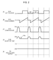
- Fig. 2 illustrates operation waveforms of various units when the power supply circuit illustrated in Fig. 1 is operated.
- 2A denotes the waveform of a voltage, which is a rectangular wave signal, applied to the gate of the field-effect transistor Q101 from the voltage controlled oscillator 101.
- the field-effect transistor Q101 When the field-effect transistor Q101 is turned on, a current flows from the power supply voltage Vcc to the inductor L100.
- the waveform of the drain current flowing through the field-effect transistor Q101 at this moment is denoted by 2B. That is, energy is accumulated in the inductor L100 in accordance with the length of time during which the current flows.
- the field-effect transistor Q101 is turned off, voltage resonance occurs between the capacitor C100 and the inductor L100.
- the waveform of the drain voltage of the field-effect transistor Q101 at this moment is denoted by 2C.
- the voltage represented by this voltage waveform is generally called a flyback voltage.
- a maximum value V1a of the flyback voltage of the resonant circuit becomes a voltage value a few times that of the power supply voltage Vcc by the voltage resonance.
- a voltage can be effectively applied to downstream circuits without performing what is called hardware switching by setting an OFF time in such a manner that the next ON time of the field-effect transistor Q101 starts when this resonant voltage becomes 0 V or less.
- the voltage generated by this resonant circuit is increased by an amount corresponding to the number of stages of the downstream stages of the multi-stage rectifier circuit.
- a voltage waveform at the anode terminal of the diode D105 arranged at the last stage of the rectifier circuit is denoted by 2D.
- This voltage waveform has a maximum voltage value V1b and has a voltage value on which the flyback voltage V1a is superimposed.
- the voltage at the cathode terminal of the diode D105 is a constant voltage V1b, and a voltage obtained by smoothing and stabilizing the voltage at the cathode terminal of the diode D105 by using the smoothing capacitor 106 has a voltage waveform denoted by 2E at the output terminal 104 (Vout).
- the rectifying-and-smoothing circuit When the field-effect transistor Q101 is turned off, the positive-polarity flyback voltage generated by the resonant circuit including the inductor L100 and the capacitor C100 is used to electrically charge the capacitor C101 via the diode D101. As a result, a maximum voltage Vmax1 is held.
- the diode D101 and capacitor C101 function as the first stage of the rectifier circuit.
- there is an effect that the peak voltage waveform of the first stage can be stabilized by connecting the capacitor C101 to the cathode terminal of the first-stage diode and the power supply voltage.
- the flyback voltage of the resonant circuit cannot be amplified by a factor of the number of stages of the rectifier circuit.
- a goal voltage output can be obtained by considering loss due to the capacity of each of the capacitors and diodes in advance.
- the voltage generated at the connection unit where the diode D105 is connected to the capacitor C105 is smoothed by the smoothing capacitor C106 and output from the output terminal 104 (Vout) as a stable voltage.
- control is performed in such a manner that the frequency of the output signal can be changed; however, the duty ratio (the ratio between the ON time and the OFF time) of the frequency is set to a fixed value.
- setting is set in such a manner that the field-effect transistor Q101 does not perform hardware switching.
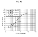
- Fig. 12 illustrates load characteristics of a typical circuit according to this embodiment.
- a case in which a load having a high resistance of 100 M ⁇ or higher is used will be described using specific numerical values.
- a frequency f 160 kHz
- the peak voltage of the flyback voltage of the voltage resonant circuit is about 180 V.
- the rectifier circuit has four stages, a voltage about three times higher than the peak voltage, that is, about 540 V is output.
- the output voltage can be controlled by changing the flyback voltage of the resonant circuit in accordance with an input frequency. For example, in a case in which the number of stages of the rectifier circuit is four, if the frequency f is 300 kHz, which is multiplied twofold, the output voltage decreases by approximately one half. In this way, a sufficiently high voltage can be generated with respect to the power supply voltage. Furthermore, an output voltage can be easily adjusted in accordance with the number of stages of the rectifier circuit and a control signal and an output voltage, and the output voltage can be adjusted to have an appropriate value in accordance with a load change.
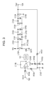
- a circuit structure of a high voltage power supply that can output a high negative voltage can be realized by, for example, a circuit illustrated in Fig. 3 .
- the diodes of the rectifier circuit are connected to each other in such a manner that the polarity of the diodes is reversed compared with the circuit structure that can output a positive voltage illustrated in Fig. 1 .
- the output-voltage detection circuit and the voltage controlled oscillator 101 should also have a circuit constant and specifications corresponding to the high negative voltage.
- targets to which a high voltage is applied in the above-described electrophotographic image formation apparatus can be applied as examples of a load to which output from the high voltage power supply described in this embodiment outputs is to be supplied.
- a charger unit (a charging roller) that charges a photoconductor drum serving as an image bearing member in a laser beam printer
- a developer unit (a developer roller) that develops an electrostatic latent image formed formed on the photoconductor drum as a result of exposure
- a transferring unit (a transferring roller) that transfers the image developed on the photoconductor drum onto a recording material, and the like can be applied as loads.
- a load that requires a high voltage and whose condition changes in accordance with an environment change can be applied.
- an output voltage can be appropriately adjusted in accordance with a load change in a high voltage power supply that does not use a transformer.
- Embodiment 2 a high voltage power supply according to Embodiment 2 will be described in accordance with operation waveforms illustrated in Fig. 4 .
- the circuit according to Embodiment 2 is similar to the circuit according to Embodiment 1 illustrated in Fig. 1 .
- the method for controlling an output voltage for Embodiment 2 is different from that for Embodiment 1.
- Embodiment 2 employs a method for controlling an output voltage in which an output voltage is controlled in such a manner that an OFF time (toff time in Fig. 4 ) of a control signal, which is input to the gate terminal of the field-effect transistor Q101, is set to a fixed value and only an ON time (ton time in Fig. 4 ) of the control signal can be changed.
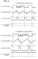
- Fig. 4 illustrates operation waveforms of various units of the circuit, which are operation waveforms according to Embodiment 2, illustrated in Fig. 1 , similarly to Embodiment 1.
- a drawing for when a low voltage is output (part A of Fig. 4 ) and a drawing for when a high voltage is output (part B of Fig. 4 ) are separate drawings.
- 4A and 4E denote the waveform of a voltage applied to the gate terminal of the field-effect transistor Q101 from the voltage controlled oscillator 101.
- a current flows from the power supply voltage Vcc to the inductor L100.
- the waveform of a drain current flowing through the field-effect transistor Q101 at this time is denoted by 4B and 4F.
- a voltage can be efficiently applied to the downstream-stage circuits without performing hardware switching by setting the next ON time of the field-effect transistor Q101 to start when this resonance voltage is 0 V or less.
- the voltage generated by this resonant circuit is increased by an amount corresponding to the number of stages of the downstream stages of the rectifier circuit.
- Waveforms obtained by smoothing and stabilizing a voltage waveform output from the rectifier circuit using the smoothing capacitor C106 are voltage waveforms denoted by 4D and 4H at the output terminal 104 (Vout). Voltages V2b (4D) and V2d (4H) are output.
- an output voltage can be controlled in such a manner that the frequency is changed to be lower when the output voltage is desired to be higher and the frequency is changed to be higher when the output voltage is desired to be lower. More specifically, when the frequency is changed to be lower, more energy is stored in the inductor L100 as the ON time ton of the field-effect transistor Q101 becomes longer. As a result, the maximum value of the flyback voltage waveform of the resonant circuit also becomes larger. That is, the voltage output from the output terminal 104 becomes higher.
- the ON time ton and the OFF time toff of the field-effect transistor Q101 similarly become shorter.
- the ON time ton and the OFF time toff similarly become shorter and the frequency becomes higher to a certain value
- the Q101 is turned on while the drain voltage of the field-effect transistor Q101 has an electric potential. That is, the field-effect transistor Q101 performs hardware switching and loss caused by the switching operation becomes greater.
- a current flows between the drain and the source at the moment when the Q101 is turned on, resulting in greater loss.
- control is performed in such a manner that the OFF time toff during which a flyback voltage is generated is set to a fixed value, the control signal is turned on after the flyback voltage decreases to 0 V or less, and only the ON time ton can be changed.
- the OFF time toff is made to be longer than a time width of a flyback voltage waveform set in accordance with the resonance frequency of the voltage resonant circuit constituted by the inductor L100 and the capacitor C100.
- the relationship between an ON time ton1 for when a low voltage is output and an ON time ton2 for when a high voltage is output is controlled to be ton1 ⁇ ton2.
- Embodiment 2 is effective in a case in which the frequency range in which control is performed and the frequency can be changed is desired to be a wider range.
- an output voltage can be appropriately adjusted in accordance with a load change in a high voltage power supply that does not use a transformer, and also hardware switching can be prevented from being performed, circuit loss can be reduced, and a stable high voltage can be output.
- Embodiment 3 will be described with reference to Figs. 5 and 6 . Note that the description about parts that are the same as circuits of the high voltage power supply according to Embodiment 1 will be omitted.
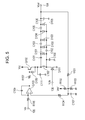
- the circuit of the high voltage power supply according to Embodiment 3 and the circuit according to Embodiment 1 differ in that Embodiment 3 employs a method for controlling an output voltage, in which an output voltage is changed by performing control in such a manner that a supply voltage can be changed in addition to the frequency control.
- the operational amplifier Q100, the resistor R106, and a capacitor C109 function as an integrator circuit. That is, the control signal Vin, which has been smoothed in accordance with an integration time constant set in accordance with the number of parts of the resistor R106 and capacitor C109, is input to the operational amplifier Q100.
- an output voltage generated at the output terminal 104 is input to the non-inverting input terminal (+ terminal) of the operational amplifier Q100 via the voltage detection resistor R101, the voltage divider resistors R102 and R103, the protect resistor 104, and the noise eliminating capacitor C107, which constitute output-voltage detection means.
- a feedback voltage to be input to the non-inverting input terminal (+ terminal) of the operational amplifier Q100 from the output-voltage detection means is adjusted to be equal to an analog voltage input to the inverting input terminal (- terminal) from the controller.
- the output voltage of the operational amplifier Q100 makes the electric potential of the base of a transistor Q102 change via a resistor R107. Furthermore, the voltage obtained by reducing the electric potential of the base of the transistor Q102 by the electric potential between the base and the emitter of the transistor Q102 is a voltage to be applied to the inductor L100.
- a capacitor C111 is connected to stabilize a supply voltage to be applied to the inductor L100 and a diode D106 is connected to protect the transistor Q102.
- the structure of the circuit serving as a voltage changing unit that changes a voltage to be applied to this inductor L100 is a feature of this Embodiment 3.
- a control frequency is input to the gate terminal of the field-effect transistor Q101 from a frequency input terminal 106 (Vclk).
- the duty ratio of this control frequency may be set to a fixed value or may be set as described in Embodiment 2 in such a manner that the duty ratio can be changed.
- a frequency that has been preset in such a manner that the field-effect transistor Q101 is prevented from performing hard switching is input from the controller (not shown) via the frequency input terminal 106 (Vclk) as a control signal, and control is performed in such a manner that the supply voltage to be applied to the inductor L100 can be changed so as to obtain a desired output voltage.
- a control signal (whose frequency can be changed) is input from the controller; however, control may be performed in such a manner that the control signal can be changed by using a voltage controlled oscillator (VCO) as described in Embodiment 1.
- VCO voltage controlled oscillator
- Fig. 6 illustrates operation waveforms of various units of the circuit illustrated in Fig. 5 and includes drawings: a drawing for when a low voltage is output (part A of Fig. 6 ) and a drawing for when a high voltage is output (part B of Fig. 6 ).
- 6A and 6F denote the waveform of a voltage applied to the gate of the field-effect transistor Q101 from the voltage controlled oscillator 101.
- the relationship between an OFF time toff3 for when a low voltage is output and an OFF time toff4 for when a high voltage is output is toff3 ⁇ toff4, and the relationship between an ON time ton3 for when a low voltage is output and an ON time ton4 for when a high voltage is output is ton3 ⁇ ton4.
- the duty ratio is set to a fixed value.
- 6B and 6G denote a voltage applied to the inductor L100 by supply-voltage changing means, which is a feature of Embodiment 3.
- the relationship between a supply voltage V3a for when a low voltage is output and a supply voltage V3d for when a high voltage is output is V3a ⁇ V3d.
- the above-described ON time toff3 for when a low voltage is output is set in such a manner that the next ON of the field-effect transistor Q101 starts when the resonant voltage is 0 V or less.
- a voltage can be efficiently applied to the downstream-stage circuits without making hardware switching be performed.
- the flyback voltage generated by the resonant circuit is increased by an amount corresponding to the number of stages of the downstream stages of the rectifier circuit.
- Voltage waveforms obtained by smoothing and stabilizing a voltage waveform output from the rectifier circuit using the smoothing capacitor C106 are voltage waveforms denoted by 6E and 6J at the output terminal 104 (Vout).
- the relationship between a supply voltage V3c for when a low voltage is output and a supply voltage V3f for when a high voltage is output is V3c ⁇ V3f.
- an output voltage can be appropriately adjusted in accordance with a load change in a high voltage power supply that does not use a transformer, and also a voltage range in which control is performed can be wider by performing control in such a manner that the supply voltage can be changed and the frequency can also be changed.
- control is performed in such a manner that the supply voltage can be changed and also the frequency can be changed
- a method in which an output voltage is controlled by setting the frequency to a fixed value and performing control in such a manner that the supply voltage can be changed is also effective.
- Embodiment 4 of the present invention will be described with reference to Figs. 7 and 8 . Note that, the description about parts that are the same as circuits of the high voltage power supply according to Embodiment 1 will be omitted.
- This Embodiment 4 and the above-described Embodiment 1 differ in that, as illustrated in the circuit of Fig. 7 , an inductor L101 is inserted in series between a connection unit that connects the inductor L100 and the capacitor C100, which constitute the voltage resonant circuit, and the rectifier circuit and a current resonant circuit is formed using the capacitance characteristics of the downstream-stage diodes and capacitors.
- Fig. 8 illustrates operation waveforms of various units illustrated in Fig. 7 .
- 8A denotes a voltage applied to the gate terminal of the field-effect transistor Q101.
- the waveform representing a drain current flowing through the field-effect transistor Q101 is denoted by 8B.
- the waveform of a drain voltage of the field-effect transistor Q101 is denoted by 8C.
- the voltage resonance makes a maximum value V4a of the flyback voltage be amplified to a voltage value a few times that of the power supply voltage Vcc.
- the waveform of a current flowing through the inductor L101 is denoted by 8D.
- this current waveform changes with a constant of the circuit.
- a current amplitude I4a of a sine wave having a constant frequency is superimposed on the current flowing through the inductor L101.
- This is a frequency component set in accordance with the capacitance characteristics of the downstream stages of the rectifier circuit and the constant of the inductor L101.
- the capacitance characteristics of diodes are generally low, and thus the resonance frequency becomes higher.
- the voltage at the output side of the inductor L101 is denoted by 8E, and a maximum value V4b of the voltage is almost the same as the maximum value V4a of the above-described flyback voltage.
- the voltage waveform changes by passing through the inductor L101 and an effective value of the flyback voltage increases.
- a voltage amplitude V4c is superimposed on an area where the flyback voltage is 0 V by the amplitude of the current having a high frequency generated in part 8E.
- the flyback voltage is changed to have a voltage waveform (a voltage waveform on a substantial sine wave) having a higher effective value by this circuit operation.
- the waveform of a voltage at the anode terminal of the diode D105 arranged at the last stage of the rectifier circuit is denoted by 8F.
- the voltage waveform has a maximum voltage value V4d, and the above-described amplitude voltage V4b is ideally superimposed on the voltage waveform.
- the voltage at the cathode terminal of the diode D105 is a constant voltage V4d.
- the voltage waveform, which is smoothed and stabilized by the smoothing capacitor C106, at the output terminal 104 (Vout) is denoted by 8G.
- an output voltage can be appropriately adjusted in accordance with a load change in a high voltage power supply that does not use a transformer, and the effective value of the flyback voltage can be increased. Thus, a higher output power can be obtained.
- Embodiment 5 will be described with reference to Figs. 9 , 10 , and 11 . Note that, the description about parts that are the same as circuits of the high voltage power supply according to Embodiment 1 will be omitted.
- This Embodiment 4 and the above-described Embodiment 1 differ in that, unlike the voltage resonant circuit of Embodiment 1 in which an inductor and a capacitor are connected in parallel, a push-pull current amplifier circuit is constituted by connecting the base of an NPN transistor Q102 to the base of a PNP transistor Q103 and connecting the emitter of the NPN transistor Q102 to the emitter of the PNP transistor Q103, the NPN transistor Q102 and PNP transistor Q103 serving as switching units (switching elements).
- a capacitor C110 is inserted between the output unit of the current amplifier circuit and the rectifier circuit, and an inductor L110 and a resistor R110 are connected in series to the ground to constitute an LCR series resonance circuit.
- a circuit using the capacitor C110, the inductor L110, and the resistor R110 is illustrated as an example of the current resonant circuit.
- this current resonant circuit The frequency characteristics of this current resonant circuit are illustrated in Fig. 10 .
- a gain (dB) reaches a maximum value at a resonance frequency f0, and the f0 is set in accordance with the constant of the inductor L110 and the constant of the capacitor C110.
- this circuit has a characteristic of a high Q.
- the resistor R110 is inserted to optimize the Q of the circuit.
- the output performance of the circuit can be improved by setting the control frequency near the resonance frequency f0.
- Fig. 11 illustrates operation waveforms of various units of the circuit illustrated in Fig. 9 .
- 11A denotes a base voltage applied to the gate terminals of the NPN transistor Q102 and PNP transistor Q103, the gate terminals being connected to each other.
- the waveform of a current flowing through the capacitor C110 is denoted by 11C.
- the phase of this current waveform is 45 degrees ahead of that of the voltage waveform obtained at the gate terminal and denoted by 11A.
- the voltage at a connection unit that connects the capacitor C110 and the inductor L110, which constitute the current resonant circuit, is denoted by 11D, and the voltage is converted into a sine wave having an amplitude voltage V5a by the current resonant circuit.
- the phase of the voltage waveform is 45 degrees behind that of the voltage waveform obtained at the gate terminal and denoted by 11A and 90 degrees behind that of the current waveform of the capacitor C110 denoted by 11C.
- a voltage waveform at the anode terminal of the diode D105 arranged at the last stage of the resonant circuit is denoted by 11E.
- the voltage waveform has a maximum voltage value V5b, and the above-described amplitude voltage V5a is ideally superimposed on the voltage waveform. Moreover, the voltage at the cathode terminal of the diode D105 is a constant voltage V5b.
- the voltage waveform, which is smoothed and stabilized by the smoothing capacitor C106, at the output terminal 104 (Vout) is denoted by 11F.
- current amplification is performed by the push-pull current resonant circuit and control is performed near the resonance frequency f0 in order to take advantage of the characteristics of the current resonant circuit, which has a high gain. Furthermore, by performing voltage amplification by the multi-stage rectifier circuit, an output voltage can be appropriately adjusted in accordance with a load change in a high voltage power supply that does not use a transformer and higher voltage power can be obtained. Moreover, the structure of the circuit according to this Embodiment 5 also has an advantage in that there is no need to use a transistor that can withstand a high voltage because current amplification is performed using the power supply voltage as is.
- Embodiment 6 a high voltage power supply according to this Embodiment 6 will be described with reference to Fig. 13 . Note that, the description about parts that are the same as circuits of the high voltage power supply according to Embodiment 1 will be omitted.
- This Embodiment 6 and the above-described Embodiment 1 differ in that the circuit according to this embodiment has two channels of a first output voltage (Vout1) and a second output voltage (Vout2). Furthermore, this embodiment is characterized in that the first output voltage is obtained from the last stage of the rectifier circuit serving as a rectifier unit and the second output voltage is obtained from the upstream portion of the rectifier circuit with respect to the last stage thereof.
- a voltage (Vout1) output from a first voltage output unit is an output from the second stage, which is the last stage, of the rectifier circuit serving as a second rectifier unit and a voltage (Vout2) output from a second voltage output unit is an output from the first stage of the rectifier circuit serving as a first rectifier unit.
- the circuit structure is simple and inexpensive in which just a C112 is used as a part for outputting a field to the Vout.
- a case in which there are two channels for output voltages has been described in this Embodiment 6, but the number of channels for output voltages is not limited to two.
- the circuit structure may have three or more channels. In this case, each of many output voltages should be obtained from a corresponding one of rectifier stages.
- an output voltage can be appropriately adjusted in accordance with a load change in a high voltage power supply that does not use a transformer, and a plurality of high voltage outputs can be obtained.
- Embodiment 7 a high voltage power supply according to Embodiment 7 will be described with reference to Fig. 14 . Note that, the description about parts that are the same as circuits of the high voltage power supply according to Embodiment 1 will be omitted. Differences between this Embodiment 7 and the above-described Embodiment 6 will be described below.
- the output voltage Vout2 can only get a value which is n times the maximum peak voltage Vmax of the flyback voltage.
- voltage divider resistor circuits are applied to make it possible to obtain arbitrary voltages other than n-fold voltages.
- a circuit structure and operation of this Embodiment 7 will be described using Fig. 14 .
- a voltage output which is n times the Vmax is obtained at the cathode side of the D105 of the circuit illustrated in Fig. 14 . That is, when a rectifier circuit has a structure in which an output Vout1 is n x Vmax, the voltage at the cathode side of the D105 is (n - 1) times the Vmax.
- an output Vout2 is a voltage obtained by dividing the voltage obtained at the anode side of the D104 by resistors R108 and R109. This Vout2 is (R109 / R108 + R109) x (n - 1) x Vmax. That is, in the circuit illustrated in Fig. 14 , two arbitrary voltage outputs as expressed by the following equation can be obtained.
- Vout ⁇ 2 R ⁇ 109 / R ⁇ 108 + R ⁇ 109 ⁇ n - 1 ⁇ Vmax
- a circuit for outputting an arbitrary voltage Vout2 which is not an integer multiple of Vmax, has a simple and inexpensive circuit structure including the R108, R109, and C112.
- Vout2 which is not an integer multiple of Vmax
- the circuit structure may have three or more channels. In this case, each of many output voltages should be obtained from a corresponding one of rectifier stages.
- an output voltage can be appropriately adjusted in accordance with a load change in a high voltage power supply that does not use a transformer, and a plurality of high voltage outputs can be obtained.
- Embodiment 8 will be described with reference to Fig. 15 . Note that, the description about parts that are the same as circuits of the high voltage power supply according to Embodiment 1 will be omitted. Differences between this Embodiment 8 and the above-described Embodiment 7 will be described below.
- the output voltage Vout2 is an arbitrary voltage obtained as a result of resistor voltage division using the R108 and R109.
- This Embodiment 8 is characterized in that an arbitrary voltage is obtained by using a Zener diode D106 as a constant voltage element.
- a circuit structure and operation will be described with reference to Fig. 15 .
- a voltage output which is n times the Vmax is obtained at the cathode side of the D105 of the circuit illustrated in Fig. 15 . That is, when a rectifier circuit has a structure in which a voltage output Vout1 is n x Vmax, the voltage at the anode side of the D104 is (n - 1) times the Vmax.
- An output Vout2 is a value obtained by subtracting a Zener voltage Vz of the Zener diode D106 from the voltage obtained at the anode side of the D104, and thus the Vout2 is (n - 1) ⁇ Vmax - Vz. That is, in the circuit illustrated in Fig. 15 , two arbitrary voltage outputs can be obtained as expressed below.
- Vout ⁇ 2 n - 1 ⁇ Vmax - Vz
- a circuit for outputting an arbitrary voltage Vout2, which is not an integer multiple of Vmax has a simple and inexpensive circuit structure including the D106, C112, and R110.
- the R110 in Fig. 15 is used to guarantee the Zener voltage of the D105. If a connected load can guarantee the Zener voltage, the R110 can be omitted.
- the number of channels for output voltages is not limited to two.
- the circuit structure may have three or more channels. In this case, each of many output voltages should be obtained from a corresponding one of rectifier stages.
- a Zener diode is used as a constant voltage element in this Embodiment 8; however, a varistor may also be used.
- an output voltage can be appropriately adjusted in accordance with a load change in a high voltage power supply that does not use a transformer, and a plurality of high voltage outputs can be obtained.
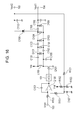
- Embodiment 9 a power supply according to Embodiment 9 will be described with reference to Fig. 16 . Note that, the description about parts that are the same as circuits of the high voltage power supply according to Embodiment 1 will be omitted. Differences between this Embodiment 9 and the above-described Embodiment 8 will be described below.
- Embodiment 9 obtains the feedback voltage from the Vout2.
- the withstand voltage of a part used in the feedback voltage channel can be lower. More specifically, the withstand voltage of the R111 can be lower and cost reduction can be realized.
- an output voltage can be appropriately adjusted in accordance with a load change in a high voltage power supply that does not use a transformer, and a plurality of high voltage outputs can be obtained.
Landscapes
- Engineering & Computer Science (AREA)
- Power Engineering (AREA)
- Dc-Dc Converters (AREA)
Abstract
Description
- The present invention relates to a high voltage power supply that generates a high voltage.
- As a conventional image formation apparatus, for example, an electrophotographic image formation apparatus includes a charging roller for charging the surface of a photoconductor drum serving as an image bearing member and a developer roller for developing an electrostatic latent image, which is formed on the photoconductor drum, by using toner serving as a developer. For example, a high voltage of about a few hundred V to a few KV (a direct-current high voltage) needs to be applied to this charging roller and this developer roller in order to charge the photoconductor drum and perform development. For generation of such a high voltage, a power supply for high-voltage generation using a wire-wound electromagnetic transformer (hereinafter referred to as a high voltage power supply) is employed.
- For example, the structure of a high voltage power supply using an electromagnetic transformer is described in
PTL 1, and a desired high voltage can be output to a load. - In contrast to the high voltage power supply using such an electromagnetic transformer, a power supply circuit that makes it possible to reduce the size and weight of a high voltage power supply circuit without using an electromagnetic transformer has been proposed (see PTL 2).
PTL 2 discloses the structure for outputting a voltage that an LC resonant circuit obtains by amplifying a voltage (24 V) from a low voltage power supply by using a clock signal serving as a control signal to a boosting circuit including a plurality of diodes and capacitors. With this structure, no transformer is used. Thus, a high voltage power supply can be smaller and lighter. -
- PTL 1: Japanese Patent Laid-Open No.
4-352181 - PTL 2: Japanese Patent Laid-Open No.
2003-189595 - However, the high voltage power supply described in
PTL 2 has the following problems. In the high voltage power supply inPTL 2, the value of a high voltage to be output to a load is a preset fixed value and a signal having a fixed frequency is used as a control signal input to an LC resonant circuit for outputting a voltage. For example, a charging roller and a developer roller serving as loads in an image formation apparatus may have a load change due to environmental variation within the apparatus or wear in the used charging roller and developer roller. If the image formation apparatus does not adjust the voltage output to the charging roller and developer roller in accordance with such a load change, a faulty image may be created in which, for example, the degree of darkness changes. For example, if the high voltage power supply circuit in citeddocument 2 is applied, it is difficult to perform adjustment in accordance with a load change. Thus, an excessive voltage or an insufficient voltage may be applied to the loads. - The present invention has been made in light of the above-described points, and an object of the present invention is to provide a high voltage power supply that can appropriately adjust an output voltage in accordance with a load change.
- A power supply according to the present invention for achieving the above-describe object is characterized by including a switching unit that is driven in accordance with a frequency signal; a voltage resonant unit that is connected to the switching unit and includes an inductor, to which a voltage is applied when the switching unit is driven, and a capacitor; a connection unit that connects the switching unit, the inductor, and the capacitor; a rectifier unit that includes a diode that is connected to the connection unit at a power-supply voltage side of the inductor via a capacitor; a voltage output unit that outputs a voltage obtained form the rectifier unit; and a frequency control unit that controls a frequency of the frequency signal in accordance with a control signal used to set a voltage output from the voltage output unit and an output signal output from the voltage output unit.
- As described above, according to the present invention, an output voltage can be appropriately adjusted in accordance with a load change in a high voltage power supply that does not use a transformer.
-
- [
Fig. 1] Fig. 1 is a circuit diagram of a power supply according toEmbodiment 1. - [
Fig. 2] Fig. 2 is a diagram of operation waveforms of the circuit illustrated inFig. 1 . - [
Fig. 3] Fig. 3 is a circuit diagram of a power supply, another embodiment, according to Embodiment 1. - [
Fig. 4] Fig. 4 includes diagrams of operation waveforms of a power supply according toEmbodiment 2. - [
Fig. 5] Fig. 5 is a circuit diagram of a power supply according to Embodiment 3. - [
Fig. 6] Fig. 6 includes diagrams of operation waveforms of the circuit illustrated inFig. 5 . - [
Fig. 7] Fig. 7 is a circuit diagram of a power supply according to Embodiment 4. - [
Fig. 8] Fig. 8 is a diagram of operation waveforms of the circuit illustrated inFig. 7 . - [
Fig. 9] Fig. 9 is a circuit diagram of a power supply according to Embodiment 5. - [
Fig. 10] Fig. 10 illustrates frequency characteristics of the circuit illustrated inFig. 9 . - [
Fig. 11] Fig. 11 is a diagram of operation waveforms of the circuit illustrated inFig. 9 . - [
Fig. 12] Fig. 12 is a diagram of load characteristics of the circuit according toEmbodiment 1. - [
Fig. 13] Fig. 13 is a circuit diagram of a power supply according to Embodiment 6. - [
Fig. 14] Fig. 14 is a circuit diagram of a power supply according to Embodiment 7. - [
Fig. 15] Fig. 15 is a circuit diagram of a power supply according to Embodiment 8. - [
Fig. 16] Fig. 16 is a circuit diagram of a power supply according to Embodiment 9. - Next, the specific structure of the present invention for solving the above-described problems will be described in accordance with embodiments below. Note that the following embodiments are but exemplifications, and do not imply that the technical scope of the present invention is restricted only thereto.
-
Fig. 1 is a diagram illustrating the structure of a power supply circuit of a power supply for generating a high voltage (hereinafter referred to as a high voltage power supply) according toEmbodiment 1. In the power supply circuit illustrated inFig. 1 , an inductor L100 and a capacitor C100 constitute a voltage resonant circuit. The inductor L100 is an element that is connected to a switching element and a power supply voltage Vcc (+24 V in this embodiment), and is an exemplary element having an inductance component to which a voltage is intermittently applied in accordance with turning on/off of the switching element. The capacitor C100 is grounded. An output from the voltage resonant circuit, which is constituted by this inductor L100 and this capacitor C100 and serves as a voltage resonant unit, is rectified and smoothed into a positive voltage by a rectifying-and-smoothing circuit. In the rectifying-and-smoothing circuit, a positive-polarity flyback voltage is extracted by a diode D101, which allows a current to pass through in a forward direction, and a capacitor C101 carrying electric charge, the capacitor C101 being connected to the cathode terminal of the diode D101 and the power supply voltage Vcc. The connection relationship between the inductor L100 and the diode D101 and capacitor C101 is as follows: the anode terminal of the diode D101 is connected to a connection unit where the inductor L100 and the capacitor C100 are connected; the cathode terminal of the diode D101 is connected to the other terminal (at the power-supply voltage side) of the inductor L100. Furthermore, a multi-stage rectifier circuit is formed by diodes D102, D103, D104, and D105 and capacitors C102, C103, C104, and C105. An output of the multi-stage rectifier circuit is grounded via a smoothing capacitor C106, and the waveform of an output voltage is smoothed. An output voltage of this multi-stage rectifier circuit is output from an output terminal 104 (Vout) serving as a voltage output unit. - Moreover, an output voltage (Vout) is input to a non-inverting input terminal (+ terminal) of an operational amplifier Q100 via a voltage detection resistor R101, voltage divider resistors R102 and R103, a
protective resistor 104, and a noise eliminating capacitor C107. This circuit is an output-voltage detection circuit. An analog signal (a control signal for controlling an output voltage of the high voltage power supply) input to an input terminal 103 (Vcont) from a controller (not shown) is input to an inverting input terminal (- terminal) of the operational amplifier Q100 via a resistor R105. The operational amplifier Q100, the resistor R105, and a capacitor C108 function as an integrator circuit. That is, the control signal Vcont, which has been smoothed in accordance with an integration time constant set in accordance with the number of parts of the resistor R105 and capacitor C108, is input to the operational amplifier Q100. In this circuit, a feedback voltage input to the non-inverting input terminal (+ terminal) of the operational amplifier Q100 from the output-voltage detection circuit is adjusted to be equal to an analog voltage input to the inverting input terminal (-terminal) from the controller. - An output terminal of the operational amplifier Q100 is connected to a voltage controlled oscillator (VCO) 101 serving as a frequency control unit that controls a drive frequency of a field-effect transistor Q101, which serves as a switching unit (the switching element). This voltage controlled oscillator 110 is an exemplary oscillator that changes and sets a frequency of a frequency signal (hereinafter referred to as an output signal) used to control the drive frequency of the field-effect transistor Q101, in accordance with the input control signal (Vcont) and the output voltage (Vout), which is detected and fed back. Furthermore, an output signal serving as a frequency signal from the voltage controlled
oscillator 101 is input to the gate terminal of the field-effect transistor Q101. The field-effect transistor Q101 is an exemplary switching element driven by a pulsed output signal output from the voltage controlledoscillator 101. The drain terminal of the field-effect transistor Q101 is connected to the voltage resonant circuit constituted by the above-described L100 and C100. The drain terminal of the field-effect transistor Q101 is connected to the power supply voltage Vcc via the inductor L100 and is grounded via the capacitor C100. Here, the source terminal of the field-effect transistor Q101 is grounded. - In this way, a voltage amplified by the voltage resonant circuit serving as the voltage resonant unit, the voltage resonant circuit being constituted by the inductor L100 and the capacitor C100, is directly rectified by a rectifier circuit serving as a rectifier unit. An output is increased to be a high voltage by using a multi-stage rectifier circuit (a plurality of rectifier circuits are connected to one another). Then, an output voltage can be adjusted to be appropriate for a load condition by controlling the frequency of the output signal at the voltage controlled oscillator (VCO) in accordance with the control signal and the output voltage.
- Next,
Fig. 2 illustrates operation waveforms of various units when the power supply circuit illustrated inFig. 1 is operated. Here, 2A denotes the waveform of a voltage, which is a rectangular wave signal, applied to the gate of the field-effect transistor Q101 from the voltage controlledoscillator 101. When the field-effect transistor Q101 is turned on, a current flows from the power supply voltage Vcc to the inductor L100. The waveform of the drain current flowing through the field-effect transistor Q101 at this moment is denoted by 2B. That is, energy is accumulated in the inductor L100 in accordance with the length of time during which the current flows. Next, when the field-effect transistor Q101 is turned off, voltage resonance occurs between the capacitor C100 and the inductor L100. The waveform of the drain voltage of the field-effect transistor Q101 at this moment is denoted by 2C. The voltage represented by this voltage waveform is generally called a flyback voltage. A maximum value V1a of the flyback voltage of the resonant circuit becomes a voltage value a few times that of the power supply voltage Vcc by the voltage resonance. Moreover, a voltage can be effectively applied to downstream circuits without performing what is called hardware switching by setting an OFF time in such a manner that the next ON time of the field-effect transistor Q101 starts when this resonant voltage becomes 0 V or less. The voltage generated by this resonant circuit is increased by an amount corresponding to the number of stages of the downstream stages of the multi-stage rectifier circuit. A voltage waveform at the anode terminal of the diode D105 arranged at the last stage of the rectifier circuit is denoted by 2D. This voltage waveform has a maximum voltage value V1b and has a voltage value on which the flyback voltage V1a is superimposed. Moreover, the voltage at the cathode terminal of the diode D105 is a constant voltage V1b, and a voltage obtained by smoothing and stabilizing the voltage at the cathode terminal of the diode D105 by using the smoothingcapacitor 106 has a voltage waveform denoted by 2E at the output terminal 104 (Vout). - Next, an operation of the rectifying-and-smoothing circuit will be specifically described. When the field-effect transistor Q101 is turned off, the positive-polarity flyback voltage generated by the resonant circuit including the inductor L100 and the capacitor C100 is used to electrically charge the capacitor C101 via the diode D101. As a result, a maximum voltage Vmax1 is held. The diode D101 and capacitor C101 function as the first stage of the rectifier circuit. Here, there is an effect that the peak voltage waveform of the first stage can be stabilized by connecting the capacitor C101 to the cathode terminal of the first-stage diode and the power supply voltage. Next, when the field-effect transistor Q101 is turned on, a counter electromotive voltage is generated by the inductor L100. At this time, electric charge moves to the capacitor C102 via the diode D102 and the capacitor C102 is electrically charged. As a result, the flyback voltage Vmax1 is applied to the capacitor C102 as the basis for the maximum voltage Vmax1 at the capacitor C101 and the maximum voltage Vmax1 is amplified to a maximum voltage Vmax2 (≈ Vmax1 × 2). This diode D102 and the capacitor C102 function as the second stage of the rectifier circuit. Furthermore, electric charge stored in the capacitor 102 as a result of charging moves to the capacitor C103 via the
diode 103 at a time at which the field-effect transistor Q101 is turned off, and the capacitor C103 is electrically charged. As a result, a maximum voltage Vmax3 (× Vmax1 × 3) is held at the capacitor C103. Thereafter, the voltage is similarly amplified by repeatedly adding a flyback voltage to a held voltage for the number of stages of the rectifier circuit with respect to the capacitor C104 and diode D104 and the capacitor C105 and diode D105. Here, when the voltage is amplified, loss due to the capacity of each of the capacitors and diodes is caused. Thus, the flyback voltage of the resonant circuit cannot be amplified by a factor of the number of stages of the rectifier circuit. However, a goal voltage output can be obtained by considering loss due to the capacity of each of the capacitors and diodes in advance. The voltage generated at the connection unit where the diode D105 is connected to the capacitor C105 is smoothed by the smoothing capacitor C106 and output from the output terminal 104 (Vout) as a stable voltage. Here, inEmbodiment 1, control is performed in such a manner that the frequency of the output signal can be changed; however, the duty ratio (the ratio between the ON time and the OFF time) of the frequency is set to a fixed value. As described above, setting is set in such a manner that the field-effect transistor Q101 does not perform hardware switching. - Here,
Fig. 12 illustrates load characteristics of a typical circuit according to this embodiment. The load characteristic illustrated inFig. 12 are characteristics in a case in which the power supply voltage is 24 V, L of the resonant circuit = 220 µH, C of the resonant circuit = 330 pH, and C of the rectifier circuit = 330 pH. A case in which a load having a high resistance of 100 MΩ or higher is used will be described using specific numerical values. When a frequency f is 160 kHz, the peak voltage of the flyback voltage of the voltage resonant circuit is about 180 V. When the rectifier circuit has four stages, a voltage about three times higher than the peak voltage, that is, about 540 V is output. Moreover, when the rectifier circuit has ten stages, a voltage about six times higher than the peak voltage, that is, about 1080 V is output. Moreover, the output voltage can be controlled by changing the flyback voltage of the resonant circuit in accordance with an input frequency. For example, in a case in which the number of stages of the rectifier circuit is four, if the frequency f is 300 kHz, which is multiplied twofold, the output voltage decreases by approximately one half. In this way, a sufficiently high voltage can be generated with respect to the power supply voltage. Furthermore, an output voltage can be easily adjusted in accordance with the number of stages of the rectifier circuit and a control signal and an output voltage, and the output voltage can be adjusted to have an appropriate value in accordance with a load change. - The above-described embodiment explains a circuit structure and a circuit operation of a high voltage power supply that can output a positive voltage, and explains voltage and current waveforms when an operation is performed. Here, a circuit structure of a high voltage power supply that can output a high negative voltage can be realized by, for example, a circuit illustrated in
Fig. 3 . InFig. 3 , the diodes of the rectifier circuit are connected to each other in such a manner that the polarity of the diodes is reversed compared with the circuit structure that can output a positive voltage illustrated inFig. 1 . In addition to this, the output-voltage detection circuit and the voltage controlledoscillator 101 should also have a circuit constant and specifications corresponding to the high negative voltage. Moreover, in a case in which the rectifier circuit has many stages, it is necessary to reverse the polarity of all the diodes compared with a case in which a positive voltage is output. This is clear by comparingFig. 1 withFig. 3 because the diodes D101, D102, D103, D104, and D105 are reversed. With the above-described structure of the power supply circuit, a stable high voltage having a negative polarity can be generated at the output terminal 104 (Vout). - Here, targets to which a high voltage is applied in the above-described electrophotographic image formation apparatus can be applied as examples of a load to which output from the high voltage power supply described in this embodiment outputs is to be supplied. For example, a charger unit (a charging roller) that charges a photoconductor drum serving as an image bearing member in a laser beam printer, a developer unit (a developer roller) that develops an electrostatic latent image formed formed on the photoconductor drum as a result of exposure, a transferring unit (a transferring roller) that transfers the image developed on the photoconductor drum onto a recording material, and the like can be applied as loads. Moreover, other than the image formation apparatus, a load that requires a high voltage and whose condition changes in accordance with an environment change can be applied.
- As described above, according to this embodiment, an output voltage can be appropriately adjusted in accordance with a load change in a high voltage power supply that does not use a transformer.
- Next, a high voltage power supply according to
Embodiment 2 will be described in accordance with operation waveforms illustrated inFig. 4 . Here, the description about parts that are the same as circuits of the high voltage power supply according toEmbodiment 1 will be omitted. The circuit according toEmbodiment 2 is similar to the circuit according toEmbodiment 1 illustrated inFig. 1 . However, the method for controlling an output voltage forEmbodiment 2 is different from that forEmbodiment 1.Embodiment 2 employs a method for controlling an output voltage in which an output voltage is controlled in such a manner that an OFF time (toff time inFig. 4 ) of a control signal, which is input to the gate terminal of the field-effect transistor Q101, is set to a fixed value and only an ON time (ton time inFig. 4 ) of the control signal can be changed. -
Fig. 4 illustrates operation waveforms of various units of the circuit, which are operation waveforms according toEmbodiment 2, illustrated inFig. 1 , similarly toEmbodiment 1. A drawing for when a low voltage is output (part A ofFig. 4 ) and a drawing for when a high voltage is output (part B ofFig. 4 ) are separate drawings. First, 4A and 4E denote the waveform of a voltage applied to the gate terminal of the field-effect transistor Q101 from the voltage controlledoscillator 101. When the field-effect transistor Q101 is turned on, a current flows from the power supply voltage Vcc to the inductor L100. The waveform of a drain current flowing through the field-effect transistor Q101 at this time is denoted by 4B and 4F. That is, in accordance with a time during which a current flows, energy is accumulated in the inductor L100. Next, when the field-effect transistor Q101 is turned off, voltage resonance occurs between the capacitor C100 and the inductor L100. The waveform of a drain voltage of the field-effect transistor Q101 at this time is denoted by 4C and 4G. The voltage having this waveform is generally called a flyback voltage. The voltage resonance makes maximum values V2a (4C) and V2c (4G) of the flyback voltage of the resonant circuit be voltage values a few times that of the power supply voltage Vcc. A voltage can be efficiently applied to the downstream-stage circuits without performing hardware switching by setting the next ON time of the field-effect transistor Q101 to start when this resonance voltage is 0 V or less. The voltage generated by this resonant circuit is increased by an amount corresponding to the number of stages of the downstream stages of the rectifier circuit. Waveforms obtained by smoothing and stabilizing a voltage waveform output from the rectifier circuit using the smoothing capacitor C106 are voltage waveforms denoted by 4D and 4H at the output terminal 104 (Vout). Voltages V2b (4D) and V2d (4H) are output. - Next, an operation performed when control is performed in such a manner that the frequency of a control signal input to the gate terminal of the field-effect transistor Q101 from the voltage controlled
oscillator 101 can be changed will be described. In frequency-based output voltage control, an output voltage can be controlled in such a manner that the frequency is changed to be lower when the output voltage is desired to be higher and the frequency is changed to be higher when the output voltage is desired to be lower. More specifically, when the frequency is changed to be lower, more energy is stored in the inductor L100 as the ON time ton of the field-effect transistor Q101 becomes longer. As a result, the maximum value of the flyback voltage waveform of the resonant circuit also becomes larger. That is, the voltage output from theoutput terminal 104 becomes higher. In contrast, when the frequency is changed to be higher, less energy is stored in the inductor L100 as the ON time ton of the field-effect transistor Q101 becomes shorter. As a result, the maximum value of the flyback voltage waveform of the resonant circuit also becomes smaller. That is, the voltage output from theoutput terminal 104 becomes lower. In this way, the output voltage can be controlled by changing the frequency. - With respect to this operation, when the frequency is changed to be higher in a state in which the duty ratio of the control signal (the ratio of the ON time to the OFF time) is set to a fixed value, the ON time ton and the OFF time toff of the field-effect transistor Q101 similarly become shorter. When the ON time ton and the OFF time toff similarly become shorter and the frequency becomes higher to a certain value, the Q101 is turned on while the drain voltage of the field-effect transistor Q101 has an electric potential. That is, the field-effect transistor Q101 performs hardware switching and loss caused by the switching operation becomes greater. As described above, when hardware switching is performed while the drain voltage is high, a current flows between the drain and the source at the moment when the Q101 is turned on, resulting in greater loss.
- Thus, in
Embodiment 2, as illustrated inFig. 4 , control is performed in such a manner that the OFF time toff during which a flyback voltage is generated is set to a fixed value, the control signal is turned on after the flyback voltage decreases to 0 V or less, and only the ON time ton can be changed. Here, the OFF time toff is made to be longer than a time width of a flyback voltage waveform set in accordance with the resonance frequency of the voltage resonant circuit constituted by the inductor L100 and the capacitor C100. Moreover, the relationship between an ON time ton1 for when a low voltage is output and an ON time ton2 for when a high voltage is output is controlled to be ton1 < ton2. - Here, even the method described in
Embodiment 1, in which control is performed in such a manner that a frequency can be changed by setting the duty ratio of the control signal to a fixed value, can perform control in such a manner that the frequency can be changed in a frequency range that does not require hardware switching; however,Embodiment 2 is effective in a case in which the frequency range in which control is performed and the frequency can be changed is desired to be a wider range. - As described above, according to this embodiment, an output voltage can be appropriately adjusted in accordance with a load change in a high voltage power supply that does not use a transformer, and also hardware switching can be prevented from being performed, circuit loss can be reduced, and a stable high voltage can be output.
- Next, Embodiment 3 will be described with reference to
Figs. 5 and6 . Note that the description about parts that are the same as circuits of the high voltage power supply according toEmbodiment 1 will be omitted. The circuit of the high voltage power supply according to Embodiment 3 and the circuit according toEmbodiment 1 differ in that Embodiment 3 employs a method for controlling an output voltage, in which an output voltage is changed by performing control in such a manner that a supply voltage can be changed in addition to the frequency control. - First, the structure and operation of the circuit according to this Embodiment 3 will be described with reference to
Fig. 5 . An analog signal (a control signal (Vin) for the high voltage power supply) input to aninput terminal 105 from a controller (not shown) is input to the inverting input terminal (- terminal) of the operational amplifier Q100 via a resistor R106. The operational amplifier Q100, the resistor R106, and a capacitor C109 function as an integrator circuit. That is, the control signal Vin, which has been smoothed in accordance with an integration time constant set in accordance with the number of parts of the resistor R106 and capacitor C109, is input to the operational amplifier Q100. On the other hand, an output voltage generated at theoutput terminal 104 is input to the non-inverting input terminal (+ terminal) of the operational amplifier Q100 via the voltage detection resistor R101, the voltage divider resistors R102 and R103, theprotect resistor 104, and the noise eliminating capacitor C107, which constitute output-voltage detection means. A feedback voltage to be input to the non-inverting input terminal (+ terminal) of the operational amplifier Q100 from the output-voltage detection means is adjusted to be equal to an analog voltage input to the inverting input terminal (- terminal) from the controller. - The output voltage of the operational amplifier Q100 makes the electric potential of the base of a transistor Q102 change via a resistor R107. Furthermore, the voltage obtained by reducing the electric potential of the base of the transistor Q102 by the electric potential between the base and the emitter of the transistor Q102 is a voltage to be applied to the inductor L100. Here, a capacitor C111 is connected to stabilize a supply voltage to be applied to the inductor L100 and a diode D106 is connected to protect the transistor Q102. The structure of the circuit serving as a voltage changing unit that changes a voltage to be applied to this inductor L100 is a feature of this Embodiment 3.
- Moreover, a control frequency is input to the gate terminal of the field-effect transistor Q101 from a frequency input terminal 106 (Vclk). The duty ratio of this control frequency may be set to a fixed value or may be set as described in
Embodiment 2 in such a manner that the duty ratio can be changed. In this Embodiment 3, a frequency that has been preset in such a manner that the field-effect transistor Q101 is prevented from performing hard switching is input from the controller (not shown) via the frequency input terminal 106 (Vclk) as a control signal, and control is performed in such a manner that the supply voltage to be applied to the inductor L100 can be changed so as to obtain a desired output voltage. In this Embodiment 3, a control signal (whose frequency can be changed) is input from the controller; however, control may be performed in such a manner that the control signal can be changed by using a voltage controlled oscillator (VCO) as described inEmbodiment 1. -
Fig. 6 illustrates operation waveforms of various units of the circuit illustrated inFig. 5 and includes drawings: a drawing for when a low voltage is output (part A ofFig. 6 ) and a drawing for when a high voltage is output (part B ofFig. 6 ). First, 6A and 6F denote the waveform of a voltage applied to the gate of the field-effect transistor Q101 from the voltage controlledoscillator 101. The relationship between an OFF time toff3 for when a low voltage is output and an OFF time toff4 for when a high voltage is output is toff3 < toff4, and the relationship between an ON time ton3 for when a low voltage is output and an ON time ton4 for when a high voltage is output is ton3 < ton4. Here, similarly toEmbodiment 1, the duty ratio is set to a fixed value. Moreover, 6B and 6G denote a voltage applied to the inductor L100 by supply-voltage changing means, which is a feature of Embodiment 3. The relationship between a supply voltage V3a for when a low voltage is output and a supply voltage V3d for when a high voltage is output is V3a < V3d. - Next, when the field-effect transistor Q101 is turned on, a current flows from the power supply voltage Vcc to the inductor L100. The waveform of a drain current flowing through the field-effect transistor Q101 at this time is denoted by 6C and 6H. The drain current changes in accordance with the supply voltage. Next, when the field-effect transistor Q101 is turned off, voltage resonance occurs between the capacitor C100 and the inductor L100. The waveform of a drain voltage of the field-effect transistor Q101 at this time is denoted by 6D and 6I. This drain voltage changes in accordance with the supply voltage and the drain current. Here, the above-described ON time toff3 for when a low voltage is output is set in such a manner that the next ON of the field-effect transistor Q101 starts when the resonant voltage is 0 V or less. As a result, a voltage can be efficiently applied to the downstream-stage circuits without making hardware switching be performed.
- The flyback voltage generated by the resonant circuit is increased by an amount corresponding to the number of stages of the downstream stages of the rectifier circuit. Voltage waveforms obtained by smoothing and stabilizing a voltage waveform output from the rectifier circuit using the smoothing capacitor C106 are voltage waveforms denoted by 6E and 6J at the output terminal 104 (Vout). The relationship between a supply voltage V3c for when a low voltage is output and a supply voltage V3f for when a high voltage is output is V3c < V3f.
- As described above, according to this embodiment, an output voltage can be appropriately adjusted in accordance with a load change in a high voltage power supply that does not use a transformer, and also a voltage range in which control is performed can be wider by performing control in such a manner that the supply voltage can be changed and the frequency can also be changed. Here, in this Embodiment 3, although it has been described that control is performed in such a manner that the supply voltage can be changed and also the frequency can be changed, a method in which an output voltage is controlled by setting the frequency to a fixed value and performing control in such a manner that the supply voltage can be changed is also effective.
- Next, Embodiment 4 of the present invention will be described with reference to
Figs. 7 and8 . Note that, the description about parts that are the same as circuits of the high voltage power supply according toEmbodiment 1 will be omitted. This Embodiment 4 and the above-describedEmbodiment 1 differ in that, as illustrated in the circuit ofFig. 7 , an inductor L101 is inserted in series between a connection unit that connects the inductor L100 and the capacitor C100, which constitute the voltage resonant circuit, and the rectifier circuit and a current resonant circuit is formed using the capacitance characteristics of the downstream-stage diodes and capacitors. -
Fig. 8 illustrates operation waveforms of various units illustrated inFig. 7 . Here, 8A denotes a voltage applied to the gate terminal of the field-effect transistor Q101. The waveform representing a drain current flowing through the field-effect transistor Q101 is denoted by 8B. The waveform of a drain voltage of the field-effect transistor Q101 is denoted by 8C. The voltage resonance makes a maximum value V4a of the flyback voltage be amplified to a voltage value a few times that of the power supply voltage Vcc. The waveform of a current flowing through the inductor L101 is denoted by 8D. Here, this current waveform changes with a constant of the circuit. A current amplitude I4a of a sine wave having a constant frequency is superimposed on the current flowing through the inductor L101. This is a frequency component set in accordance with the capacitance characteristics of the downstream stages of the rectifier circuit and the constant of the inductor L101. The capacitance characteristics of diodes are generally low, and thus the resonance frequency becomes higher. The voltage at the output side of the inductor L101 is denoted by 8E, and a maximum value V4b of the voltage is almost the same as the maximum value V4a of the above-described flyback voltage. However, the voltage waveform changes by passing through the inductor L101 and an effective value of the flyback voltage increases. Furthermore, a voltage amplitude V4c is superimposed on an area where the flyback voltage is 0 V by the amplitude of the current having a high frequency generated inpart 8E. The flyback voltage is changed to have a voltage waveform (a voltage waveform on a substantial sine wave) having a higher effective value by this circuit operation. The waveform of a voltage at the anode terminal of the diode D105 arranged at the last stage of the rectifier circuit is denoted by 8F. The voltage waveform has a maximum voltage value V4d, and the above-described amplitude voltage V4b is ideally superimposed on the voltage waveform. Moreover, the voltage at the cathode terminal of the diode D105 is a constant voltage V4d. The voltage waveform, which is smoothed and stabilized by the smoothing capacitor C106, at the output terminal 104 (Vout) is denoted by 8G. - As described above, according to this embodiment, an output voltage can be appropriately adjusted in accordance with a load change in a high voltage power supply that does not use a transformer, and the effective value of the flyback voltage can be increased. Thus, a higher output power can be obtained.
- Next, Embodiment 5 will be described with reference to
Figs. 9 ,10 , and11 . Note that, the description about parts that are the same as circuits of the high voltage power supply according toEmbodiment 1 will be omitted. This Embodiment 4 and the above-describedEmbodiment 1 differ in that, unlike the voltage resonant circuit ofEmbodiment 1 in which an inductor and a capacitor are connected in parallel, a push-pull current amplifier circuit is constituted by connecting the base of an NPN transistor Q102 to the base of a PNP transistor Q103 and connecting the emitter of the NPN transistor Q102 to the emitter of the PNP transistor Q103, the NPN transistor Q102 and PNP transistor Q103 serving as switching units (switching elements). Furthermore, a capacitor C110 is inserted between the output unit of the current amplifier circuit and the rectifier circuit, and an inductor L110 and a resistor R110 are connected in series to the ground to constitute an LCR series resonance circuit. In this Embodiment 3, a circuit using the capacitor C110, the inductor L110, and the resistor R110 is illustrated as an example of the current resonant circuit. - The frequency characteristics of this current resonant circuit are illustrated in
Fig. 10 . A gain (dB) reaches a maximum value at a resonance frequency f0, and the f0 is set in accordance with the constant of the inductor L110 and the constant of the capacitor C110. Moreover, it is clear that this circuit has a characteristic of a high Q. In order to achieve better control, it is desirable that the resistor R110 is inserted to optimize the Q of the circuit. Thus, the output performance of the circuit can be improved by setting the control frequency near the resonance frequency f0. -
Fig. 11 illustrates operation waveforms of various units of the circuit illustrated inFig. 9 . Here, 11A denotes a base voltage applied to the gate terminals of the NPN transistor Q102 and PNP transistor Q103, the gate terminals being connected to each other. The emitter voltage at the emitter terminals of the NPN transistor Q102 and PNP transistor Q103, the emitter terminals being connected to each other, is denoted by 11B. Since the current amplifier circuit is formed, the gate terminal and the emitter terminal have substantially the same voltage. The waveform of a current flowing through the capacitor C110 is denoted by 11C. The phase of this current waveform is 45 degrees ahead of that of the voltage waveform obtained at the gate terminal and denoted by 11A. The voltage at a connection unit that connects the capacitor C110 and the inductor L110, which constitute the current resonant circuit, is denoted by 11D, and the voltage is converted into a sine wave having an amplitude voltage V5a by the current resonant circuit. The phase of the voltage waveform is 45 degrees behind that of the voltage waveform obtained at the gate terminal and denoted by 11A and 90 degrees behind that of the current waveform of the capacitor C110 denoted by 11C. A voltage waveform at the anode terminal of the diode D105 arranged at the last stage of the resonant circuit is denoted by 11E. The voltage waveform has a maximum voltage value V5b, and the above-described amplitude voltage V5a is ideally superimposed on the voltage waveform. Moreover, the voltage at the cathode terminal of the diode D105 is a constant voltage V5b. The voltage waveform, which is smoothed and stabilized by the smoothing capacitor C106, at the output terminal 104 (Vout) is denoted by 11F. - As described above, according to this embodiment, current amplification is performed by the push-pull current resonant circuit and control is performed near the resonance frequency f0 in order to take advantage of the characteristics of the current resonant circuit, which has a high gain. Furthermore, by performing voltage amplification by the multi-stage rectifier circuit, an output voltage can be appropriately adjusted in accordance with a load change in a high voltage power supply that does not use a transformer and higher voltage power can be obtained. Moreover, the structure of the circuit according to this Embodiment 5 also has an advantage in that there is no need to use a transistor that can withstand a high voltage because current amplification is performed using the power supply voltage as is.
- Next, a high voltage power supply according to this Embodiment 6 will be described with reference to
Fig. 13 . Note that, the description about parts that are the same as circuits of the high voltage power supply according toEmbodiment 1 will be omitted. This Embodiment 6 and the above-describedEmbodiment 1 differ in that the circuit according to this embodiment has two channels of a first output voltage (Vout1) and a second output voltage (Vout2). Furthermore, this embodiment is characterized in that the first output voltage is obtained from the last stage of the rectifier circuit serving as a rectifier unit and the second output voltage is obtained from the upstream portion of the rectifier circuit with respect to the last stage thereof. For example, when the rectifier circuit has two stages, a voltage (Vout1) output from a first voltage output unit is an output from the second stage, which is the last stage, of the rectifier circuit serving as a second rectifier unit and a voltage (Vout2) output from a second voltage output unit is an output from the first stage of the rectifier circuit serving as a first rectifier unit. - A circuit structure and an operation will be described with reference to
Fig. 13 . As described inEmbodiment 1, according to an ideal operation of the rectifier circuit, a DC output, which is n times the flyback voltage Vmax, can be obtained (where n is an integer). More specifically, an output which is twice the Vmax can be obtained at the cathode side of the D103 illustrated inFig. 13 . Here, if an output which is n times the Vmax is obtained at the cathode side of the D105 of the circuit illustrated inFig. 13 , that is, if a rectifier circuit has a structure in which an output Vout1 is n or Vmax x n, an output Vout2 is (n - 1) times the Vmax. Thus, two arbitrary voltage outputs as expressed below can be obtained from the circuit illustrated inFig. 13 .

(n is an integer) - Moreover, the circuit structure is simple and inexpensive in which just a C112 is used as a part for outputting a field to the Vout. Here, a case in which there are two channels for output voltages has been described in this Embodiment 6, but the number of channels for output voltages is not limited to two. The circuit structure may have three or more channels. In this case, each of many output voltages should be obtained from a corresponding one of rectifier stages.
- As described above, according to this embodiment, an output voltage can be appropriately adjusted in accordance with a load change in a high voltage power supply that does not use a transformer, and a plurality of high voltage outputs can be obtained.
- Next, a high voltage power supply according to Embodiment 7 will be described with reference to
Fig. 14 . Note that, the description about parts that are the same as circuits of the high voltage power supply according toEmbodiment 1 will be omitted. Differences between this Embodiment 7 and the above-described Embodiment 6 will be described below. - In the circuit described in Embodiment 6 and illustrated in
Fig. 13 , as expressed by Eq. 2, the output voltage Vout2 can only get a value which is n times the maximum peak voltage Vmax of the flyback voltage. In this Embodiment 7 illustrated inFig. 14 , voltage divider resistor circuits are applied to make it possible to obtain arbitrary voltages other than n-fold voltages. - A circuit structure and operation of this Embodiment 7 will be described using
Fig. 14 . A voltage output which is n times the Vmax is obtained at the cathode side of the D105 of the circuit illustrated inFig. 14 . That is, when a rectifier circuit has a structure in which an output Vout1 is n x Vmax, the voltage at the cathode side of the D105 is (n - 1) times the Vmax. Then, an output Vout2 is a voltage obtained by dividing the voltage obtained at the anode side of the D104 by resistors R108 and R109. This Vout2 is (R109 / R108 + R109) x (n - 1) x Vmax. That is, in the circuit illustrated inFig. 14 , two arbitrary voltage outputs as expressed by the following equation can be obtained.
- Furthermore, a circuit for outputting an arbitrary voltage Vout2, which is not an integer multiple of Vmax, has a simple and inexpensive circuit structure including the R108, R109, and C112. Here, a case in which there are two channels for output voltages has been described in this Embodiment 7, but the number of channels for output voltages is not limited to two. The circuit structure may have three or more channels. In this case, each of many output voltages should be obtained from a corresponding one of rectifier stages.
- As described above, according to this embodiment, an output voltage can be appropriately adjusted in accordance with a load change in a high voltage power supply that does not use a transformer, and a plurality of high voltage outputs can be obtained.
- Next, Embodiment 8 will be described with reference to
Fig. 15 . Note that, the description about parts that are the same as circuits of the high voltage power supply according toEmbodiment 1 will be omitted. Differences between this Embodiment 8 and the above-described Embodiment 7 will be described below. - In the circuit described in Embodiment 7 and illustrated in
Fig. 14 , as expressed by (Eq. 3), the output voltage Vout2 is an arbitrary voltage obtained as a result of resistor voltage division using the R108 and R109. This Embodiment 8 is characterized in that an arbitrary voltage is obtained by using a Zener diode D106 as a constant voltage element. - A circuit structure and operation will be described with reference to
Fig. 15 . A voltage output which is n times the Vmax is obtained at the cathode side of the D105 of the circuit illustrated inFig. 15 . That is, when a rectifier circuit has a structure in which a voltage output Vout1 is n x Vmax, the voltage at the anode side of the D104 is (n - 1) times the Vmax. An output Vout2 is a value obtained by subtracting a Zener voltage Vz of the Zener diode D106 from the voltage obtained at the anode side of the D104, and thus the Vout2 is (n - 1) × Vmax - Vz. That is, in the circuit illustrated inFig. 15 , two arbitrary voltage outputs can be obtained as expressed below.
- Furthermore, a circuit for outputting an arbitrary voltage Vout2, which is not an integer multiple of Vmax, has a simple and inexpensive circuit structure including the D106, C112, and R110.
- Here, the R110 in
Fig. 15 is used to guarantee the Zener voltage of the D105. If a connected load can guarantee the Zener voltage, the R110 can be omitted. Here, a case in which there are two channels for output voltages has been described in this Embodiment 8, but the number of channels for output voltages is not limited to two. The circuit structure may have three or more channels. In this case, each of many output voltages should be obtained from a corresponding one of rectifier stages. Moreover, a Zener diode is used as a constant voltage element in this Embodiment 8; however, a varistor may also be used. - As described above, according to this embodiment, an output voltage can be appropriately adjusted in accordance with a load change in a high voltage power supply that does not use a transformer, and a plurality of high voltage outputs can be obtained.
- Next, a power supply according to Embodiment 9 will be described with reference to
Fig. 16 . Note that, the description about parts that are the same as circuits of the high voltage power supply according toEmbodiment 1 will be omitted. Differences between this Embodiment 9 and the above-described Embodiment 8 will be described below. - In the circuit described in Embodiment 8 and illustrated in
Fig. 15 , a feedback voltage to be fed back to the operational amplifier Q100 was obtained from the Vout1 to compensate output voltage fluctuations. However, this Embodiment 9 obtains the feedback voltage from the Vout2. With this structure, the withstand voltage of a part used in the feedback voltage channel can be lower. More specifically, the withstand voltage of the R111 can be lower and cost reduction can be realized. - Moreover, in the circuits illustrated in
Figs. 13 and14 , similarly to this Embodiment 9, cost reduction can be realized by obtaining the feedback voltage from the Vout2. Here, a case in which there are two channels for output voltages has been described in this Embodiment 9, but the number of channels for output voltages is not limited to two. The circuit structure may have three or more channels. In this case, each of many output voltages should be obtained from a corresponding one of rectifier stages. - As described above, according to this embodiment, an output voltage can be appropriately adjusted in accordance with a load change in a high voltage power supply that does not use a transformer, and a plurality of high voltage outputs can be obtained.
-
- 100
- VCO
- L100
- inductor
- Q101
- field-effect transistor
- C100, C101, C102, C103, C104, C105
- capacitor
- D101, D102, D103, D104, D105
- diode
Claims (10)
- A high voltage power supply, comprising:a switching unit that is driven in accordance with a frequency signal;a voltage resonant unit that is connected to the switching unit and includes an inductor, to which a voltage is applied when the switching unit is driven, and a capacitor;a connection unit that connects the switching unit, the inductor, and the capacitor;a rectifier unit that includes a diode that is connected to the connection unit at a power-supply voltage side of the inductor via a capacitor;a voltage output unit that outputs a voltage obtained form the rectifier unit; anda frequency control unit that controls a frequency of the frequency signal in accordance with a control signal used to set a voltage output from the voltage output unit and an output signal output from the voltage output unit.
- The high voltage power supply according to claim 1, wherein the frequency signal is a rectangular wave signal, and
the frequency control unit controls a voltage from the voltage output unit by changing an ON time of the rectangular wave. - The high voltage power supply according to claim 1 or 2, further comprising a voltage changing unit that changes and sets a power supply voltage to be applied to the switching unit, wherein the voltage from the voltage output unit is controlled by changing the power supply voltage applied to the switching unit by using the voltage changing unit.
- The high voltage power supply according to any one of claims 1 to 3, wherein the connection unit that connects the switching unit, the inductor, and the capacitor and the diode are connected via another inductor.
- The high voltage power supply according to any one of claims 1 to 4, wherein the switching unit includes a field-effect transistor.
- The high voltage power supply according to any one of claims 1 to 4, wherein the switching unit includes a push-pull current amplifier circuit that includes an NPN transistor and a PNP transistor.
- The high voltage power supply according to claim 1, wherein the rectifier unit is one of a plurality of rectifier units connected to each other, and
the plurality of rectifier units includes a first rectifier unit connected to the switching unit and a second rectifier unit connected to the first rectifier unit, and the high voltage power supply further comprising a second voltage output unit that outputs a voltage obtained from the first rectifier circuit. - The high voltage power supply according to claim 7, wherein the second voltage output unit includes a capacitor.
- The high voltage power supply according to claim 8, wherein the second voltage output unit further includes a resistor.
- The high voltage power supply according to claim 8, wherein the second voltage output unit further includes a resistor and a constant voltage element.
Applications Claiming Priority (1)
| Application Number | Priority Date | Filing Date | Title |
|---|---|---|---|
| PCT/JP2009/071706 WO2011077583A1 (en) | 2009-12-26 | 2009-12-26 | High-voltage power supply |
Publications (3)
| Publication Number | Publication Date |
|---|---|
| EP2518876A1 true EP2518876A1 (en) | 2012-10-31 |
| EP2518876A4 EP2518876A4 (en) | 2018-01-10 |
| EP2518876B1 EP2518876B1 (en) | 2021-07-14 |
Family
ID=44187360
Family Applications (1)
| Application Number | Title | Priority Date | Filing Date |
|---|---|---|---|
| EP09852598.3A Active EP2518876B1 (en) | 2009-12-26 | 2009-12-26 | High-voltage power supply |
Country Status (6)
| Country | Link |
|---|---|
| US (2) | US8102685B2 (en) |
| EP (1) | EP2518876B1 (en) |
| JP (1) | JP5627607B2 (en) |
| KR (2) | KR101504808B1 (en) |
| CN (1) | CN102656786B (en) |
| WO (1) | WO2011077583A1 (en) |
Families Citing this family (11)
| Publication number | Priority date | Publication date | Assignee | Title |
|---|---|---|---|---|
| JP4912487B2 (en) * | 2010-07-09 | 2012-04-11 | キヤノン株式会社 | High voltage power supply |
| KR20150053503A (en) * | 2013-11-08 | 2015-05-18 | 삼성전기주식회사 | Power supply |
| JP6074397B2 (en) * | 2014-10-02 | 2017-02-01 | キヤノン株式会社 | Power supply and image forming apparatus |
| US9582016B2 (en) * | 2015-02-05 | 2017-02-28 | Silicon Laboratories Inc. | Boost converter with capacitive boost stages |
| TWI573381B (en) * | 2015-09-03 | 2017-03-01 | 財團法人國家實驗研究院 | Master-slave voltage doubling full-wave rectifier for wireless power transfer system |
| CN105553255B (en) * | 2016-01-28 | 2017-11-28 | 杨磊 | A kind of constant service time method for controlling frequency conversion for Switching capacitors |
| US11235436B2 (en) | 2016-07-08 | 2022-02-01 | Saint-Gobain Abrasives, Inc. | Abrasive articles and methods of forming the same |
| JP6953176B2 (en) * | 2017-05-18 | 2021-10-27 | キヤノン株式会社 | Power supply and image forming equipment |
| JP6866231B2 (en) * | 2017-05-18 | 2021-04-28 | キヤノン株式会社 | Power supply and image forming equipment |
| CN110138383B (en) * | 2018-02-09 | 2023-09-05 | 海能达通信股份有限公司 | Frequency generation circuit |
| CN108599591B (en) * | 2018-06-06 | 2023-08-25 | 三峡大学 | Self-current-sharing modularized high-capacity high-boost rectifier |
Family Cites Families (15)
| Publication number | Priority date | Publication date | Assignee | Title |
|---|---|---|---|---|
| US3036259A (en) * | 1958-09-23 | 1962-05-22 | Heilpern Walter | Method and means for the compensation of reactive currents due to stray capacitancesbetween the capacitor columns of a cascade rectifier |
| US4926304A (en) * | 1988-06-30 | 1990-05-15 | U.S. Philips Corporation | Switched-mode power supply with low loss interrupted oscillation |
| JP3260776B2 (en) | 1991-05-30 | 2002-02-25 | キヤノン株式会社 | Power supply circuit of image forming apparatus |
| JPH0993914A (en) * | 1995-09-22 | 1997-04-04 | Toshiba Corp | Multi-output DC / DC converter |
| US5959439A (en) * | 1997-05-23 | 1999-09-28 | The Board Of Trustees Of The University Of Illinois | Monolithic DC to DC converter |
| US5909362A (en) * | 1998-01-12 | 1999-06-01 | Eldec Corporation | Resonant power converter |
| JP2000203014A (en) * | 1999-01-08 | 2000-07-25 | Fujitsu Ltd | Head drive circuit and ink jet printer having the same |
| JP3937831B2 (en) * | 2001-12-18 | 2007-06-27 | 富士ゼロックス株式会社 | Power supply device and image forming apparatus using the same |
| JP2004048952A (en) * | 2002-07-15 | 2004-02-12 | Totoku Electric Co Ltd | High voltage power supply |
| US7477529B2 (en) * | 2002-11-01 | 2009-01-13 | Honeywell International Inc. | High-voltage power supply |
| JP4418689B2 (en) * | 2004-02-04 | 2010-02-17 | キヤノン株式会社 | Image forming apparatus |
| JP2007189880A (en) * | 2006-01-16 | 2007-07-26 | Canon Inc | High voltage power supply device and image forming apparatus having the same |
| MX2009000225A (en) | 2006-06-26 | 2009-07-15 | Battelle Memorial Institute | High voltage power supply. |
| CN101127483B (en) * | 2006-08-18 | 2010-06-16 | 盛群半导体股份有限公司 | Power supply for field emission display |
| JP4365873B2 (en) * | 2007-06-06 | 2009-11-18 | 株式会社東芝 | Voltage supply circuit and semiconductor memory device |
-
2009
- 2009-12-26 WO PCT/JP2009/071706 patent/WO2011077583A1/en not_active Ceased
- 2009-12-26 EP EP09852598.3A patent/EP2518876B1/en active Active
- 2009-12-26 JP JP2011547192A patent/JP5627607B2/en active Active
- 2009-12-26 KR KR1020127018831A patent/KR101504808B1/en active Active
- 2009-12-26 CN CN200980163054.7A patent/CN102656786B/en active Active
- 2009-12-26 KR KR1020147033809A patent/KR101600227B1/en active Active
-
2010
- 2010-12-17 US US12/972,165 patent/US8102685B2/en active Active
-
2011
- 2011-12-20 US US13/331,986 patent/US8325503B2/en active Active
Non-Patent Citations (1)
| Title |
|---|
| See references of WO2011077583A1 * |
Also Published As
| Publication number | Publication date |
|---|---|
| WO2011077583A1 (en) | 2011-06-30 |
| KR101504808B1 (en) | 2015-03-20 |
| US8325503B2 (en) | 2012-12-04 |
| EP2518876B1 (en) | 2021-07-14 |
| KR20120094521A (en) | 2012-08-24 |
| US8102685B2 (en) | 2012-01-24 |
| US20110157933A1 (en) | 2011-06-30 |
| KR20140146230A (en) | 2014-12-24 |
| JP5627607B2 (en) | 2014-11-19 |
| CN102656786A (en) | 2012-09-05 |
| KR101600227B1 (en) | 2016-03-04 |
| EP2518876A4 (en) | 2018-01-10 |
| CN102656786B (en) | 2016-04-20 |
| JPWO2011077583A1 (en) | 2013-05-02 |
| US20120087162A1 (en) | 2012-04-12 |
Similar Documents
| Publication | Publication Date | Title |
|---|---|---|
| EP2518876B1 (en) | High-voltage power supply | |
| KR100801498B1 (en) | Switching control circuit and self-contained DC-DC converter | |
| KR100744592B1 (en) | Dc-dc converter, dc-dc converter control circuit, and dc-dc converter control method | |
| US6642696B2 (en) | DC-DC converter with a feedback controller | |
| US10122278B1 (en) | Control circuit operating in pulse skip mode and voltage converter having the same | |
| WO2002001309A2 (en) | Power factor correction control circuit for switching power supply | |
| JP4666345B2 (en) | Charge pump circuit | |
| JP4997122B2 (en) | Power supply circuit and operation control method thereof | |
| EP0974186B1 (en) | Method and arrangement in a dc-to-dc converter | |
| KR101504847B1 (en) | High-voltage power source | |
| JP2002233138A (en) | Switching power supply | |
| JP6218466B2 (en) | High voltage power supply device and image forming apparatus | |
| JP6074397B2 (en) | Power supply and image forming apparatus | |
| US12431796B2 (en) | Frequency lock loop for constant switching frequency of DC-DC converters | |
| CN105871199B (en) | high voltage power supply | |
| JP3863663B2 (en) | Amplifier circuit | |
| JP3228412B2 (en) | Switching power supply | |
| JP4480682B2 (en) | High voltage generation circuit | |
| US11451146B2 (en) | DC-DC converter | |
| JPH08317650A (en) | Switching power supply | |
| JP4024732B2 (en) | Switching power supply control circuit | |
| JP6066651B2 (en) | Power supply device and image forming apparatus | |
| JPH0570192U (en) | Switching power supply | |
| JP2008253043A (en) | Power factor correction circuit | |
| JPH11122922A (en) | Switching regulator device |
Legal Events
| Date | Code | Title | Description |
|---|---|---|---|
| PUAI | Public reference made under article 153(3) epc to a published international application that has entered the european phase |
Free format text: ORIGINAL CODE: 0009012 |
|
| 17P | Request for examination filed |
Effective date: 20120726 |
|
| AK | Designated contracting states |
Kind code of ref document: A1 Designated state(s): AT BE BG CH CY CZ DE DK EE ES FI FR GB GR HR HU IE IS IT LI LT LU LV MC MK MT NL NO PL PT RO SE SI SK SM TR |
|
| DAX | Request for extension of the european patent (deleted) | ||
| RA4 | Supplementary search report drawn up and despatched (corrected) |
Effective date: 20171208 |
|
| RIC1 | Information provided on ipc code assigned before grant |
Ipc: H02M 3/07 20060101AFI20171204BHEP Ipc: H02M 7/10 20060101ALI20171204BHEP Ipc: H02M 3/155 20060101ALI20171204BHEP |
|
| STAA | Information on the status of an ep patent application or granted ep patent |
Free format text: STATUS: EXAMINATION IS IN PROGRESS |
|
| 17Q | First examination report despatched |
Effective date: 20190513 |
|
| GRAP | Despatch of communication of intention to grant a patent |
Free format text: ORIGINAL CODE: EPIDOSNIGR1 |
|
| STAA | Information on the status of an ep patent application or granted ep patent |
Free format text: STATUS: GRANT OF PATENT IS INTENDED |
|
| INTG | Intention to grant announced |
Effective date: 20210210 |
|
| GRAS | Grant fee paid |
Free format text: ORIGINAL CODE: EPIDOSNIGR3 |
|
| GRAA | (expected) grant |
Free format text: ORIGINAL CODE: 0009210 |
|
| STAA | Information on the status of an ep patent application or granted ep patent |
Free format text: STATUS: THE PATENT HAS BEEN GRANTED |
|
| AK | Designated contracting states |
Kind code of ref document: B1 Designated state(s): AT BE BG CH CY CZ DE DK EE ES FI FR GB GR HR HU IE IS IT LI LT LU LV MC MK MT NL NO PL PT RO SE SI SK SM TR |
|
| REG | Reference to a national code |
Ref country code: GB Ref legal event code: FG4D |
|
| REG | Reference to a national code |
Ref country code: IE Ref legal event code: FG4D |
|
| REG | Reference to a national code |
Ref country code: DE Ref legal event code: R096 Ref document number: 602009063885 Country of ref document: DE |
|
| REG | Reference to a national code |
Ref country code: AT Ref legal event code: REF Ref document number: 1411427 Country of ref document: AT Kind code of ref document: T Effective date: 20210815 |
|
| REG | Reference to a national code |
Ref country code: LT Ref legal event code: MG9D |
|
| REG | Reference to a national code |
Ref country code: NL Ref legal event code: MP Effective date: 20210714 |
|
| REG | Reference to a national code |
Ref country code: AT Ref legal event code: MK05 Ref document number: 1411427 Country of ref document: AT Kind code of ref document: T Effective date: 20210714 |
|
| PG25 | Lapsed in a contracting state [announced via postgrant information from national office to epo] |
Ref country code: HR Free format text: LAPSE BECAUSE OF FAILURE TO SUBMIT A TRANSLATION OF THE DESCRIPTION OR TO PAY THE FEE WITHIN THE PRESCRIBED TIME-LIMIT Effective date: 20210714 Ref country code: SE Free format text: LAPSE BECAUSE OF FAILURE TO SUBMIT A TRANSLATION OF THE DESCRIPTION OR TO PAY THE FEE WITHIN THE PRESCRIBED TIME-LIMIT Effective date: 20210714 Ref country code: AT Free format text: LAPSE BECAUSE OF FAILURE TO SUBMIT A TRANSLATION OF THE DESCRIPTION OR TO PAY THE FEE WITHIN THE PRESCRIBED TIME-LIMIT Effective date: 20210714 Ref country code: BG Free format text: LAPSE BECAUSE OF FAILURE TO SUBMIT A TRANSLATION OF THE DESCRIPTION OR TO PAY THE FEE WITHIN THE PRESCRIBED TIME-LIMIT Effective date: 20211014 Ref country code: LT Free format text: LAPSE BECAUSE OF FAILURE TO SUBMIT A TRANSLATION OF THE DESCRIPTION OR TO PAY THE FEE WITHIN THE PRESCRIBED TIME-LIMIT Effective date: 20210714 Ref country code: NO Free format text: LAPSE BECAUSE OF FAILURE TO SUBMIT A TRANSLATION OF THE DESCRIPTION OR TO PAY THE FEE WITHIN THE PRESCRIBED TIME-LIMIT Effective date: 20211014 Ref country code: PT Free format text: LAPSE BECAUSE OF FAILURE TO SUBMIT A TRANSLATION OF THE DESCRIPTION OR TO PAY THE FEE WITHIN THE PRESCRIBED TIME-LIMIT Effective date: 20211115 Ref country code: NL Free format text: LAPSE BECAUSE OF FAILURE TO SUBMIT A TRANSLATION OF THE DESCRIPTION OR TO PAY THE FEE WITHIN THE PRESCRIBED TIME-LIMIT Effective date: 20210714 Ref country code: FI Free format text: LAPSE BECAUSE OF FAILURE TO SUBMIT A TRANSLATION OF THE DESCRIPTION OR TO PAY THE FEE WITHIN THE PRESCRIBED TIME-LIMIT Effective date: 20210714 Ref country code: ES Free format text: LAPSE BECAUSE OF FAILURE TO SUBMIT A TRANSLATION OF THE DESCRIPTION OR TO PAY THE FEE WITHIN THE PRESCRIBED TIME-LIMIT Effective date: 20210714 |
|
| PG25 | Lapsed in a contracting state [announced via postgrant information from national office to epo] |
Ref country code: PL Free format text: LAPSE BECAUSE OF FAILURE TO SUBMIT A TRANSLATION OF THE DESCRIPTION OR TO PAY THE FEE WITHIN THE PRESCRIBED TIME-LIMIT Effective date: 20210714 Ref country code: LV Free format text: LAPSE BECAUSE OF FAILURE TO SUBMIT A TRANSLATION OF THE DESCRIPTION OR TO PAY THE FEE WITHIN THE PRESCRIBED TIME-LIMIT Effective date: 20210714 Ref country code: GR Free format text: LAPSE BECAUSE OF FAILURE TO SUBMIT A TRANSLATION OF THE DESCRIPTION OR TO PAY THE FEE WITHIN THE PRESCRIBED TIME-LIMIT Effective date: 20211015 |
|
| REG | Reference to a national code |
Ref country code: DE Ref legal event code: R097 Ref document number: 602009063885 Country of ref document: DE |
|
| PG25 | Lapsed in a contracting state [announced via postgrant information from national office to epo] |
Ref country code: DK Free format text: LAPSE BECAUSE OF FAILURE TO SUBMIT A TRANSLATION OF THE DESCRIPTION OR TO PAY THE FEE WITHIN THE PRESCRIBED TIME-LIMIT Effective date: 20210714 |
|
| PLBE | No opposition filed within time limit |
Free format text: ORIGINAL CODE: 0009261 |
|
| STAA | Information on the status of an ep patent application or granted ep patent |
Free format text: STATUS: NO OPPOSITION FILED WITHIN TIME LIMIT |
|
| PG25 | Lapsed in a contracting state [announced via postgrant information from national office to epo] |
Ref country code: SM Free format text: LAPSE BECAUSE OF FAILURE TO SUBMIT A TRANSLATION OF THE DESCRIPTION OR TO PAY THE FEE WITHIN THE PRESCRIBED TIME-LIMIT Effective date: 20210714 Ref country code: SK Free format text: LAPSE BECAUSE OF FAILURE TO SUBMIT A TRANSLATION OF THE DESCRIPTION OR TO PAY THE FEE WITHIN THE PRESCRIBED TIME-LIMIT Effective date: 20210714 Ref country code: RO Free format text: LAPSE BECAUSE OF FAILURE TO SUBMIT A TRANSLATION OF THE DESCRIPTION OR TO PAY THE FEE WITHIN THE PRESCRIBED TIME-LIMIT Effective date: 20210714 Ref country code: EE Free format text: LAPSE BECAUSE OF FAILURE TO SUBMIT A TRANSLATION OF THE DESCRIPTION OR TO PAY THE FEE WITHIN THE PRESCRIBED TIME-LIMIT Effective date: 20210714 Ref country code: CZ Free format text: LAPSE BECAUSE OF FAILURE TO SUBMIT A TRANSLATION OF THE DESCRIPTION OR TO PAY THE FEE WITHIN THE PRESCRIBED TIME-LIMIT Effective date: 20210714 |
|
| 26N | No opposition filed |
Effective date: 20220419 |
|
| PG25 | Lapsed in a contracting state [announced via postgrant information from national office to epo] |
Ref country code: MC Free format text: LAPSE BECAUSE OF FAILURE TO SUBMIT A TRANSLATION OF THE DESCRIPTION OR TO PAY THE FEE WITHIN THE PRESCRIBED TIME-LIMIT Effective date: 20210714 Ref country code: IT Free format text: LAPSE BECAUSE OF FAILURE TO SUBMIT A TRANSLATION OF THE DESCRIPTION OR TO PAY THE FEE WITHIN THE PRESCRIBED TIME-LIMIT Effective date: 20210714 |
|
| REG | Reference to a national code |
Ref country code: CH Ref legal event code: PL |
|
| REG | Reference to a national code |
Ref country code: BE Ref legal event code: MM Effective date: 20211231 |
|
| PG25 | Lapsed in a contracting state [announced via postgrant information from national office to epo] |
Ref country code: LU Free format text: LAPSE BECAUSE OF NON-PAYMENT OF DUE FEES Effective date: 20211226 Ref country code: IE Free format text: LAPSE BECAUSE OF NON-PAYMENT OF DUE FEES Effective date: 20211226 |
|
| PG25 | Lapsed in a contracting state [announced via postgrant information from national office to epo] |
Ref country code: FR Free format text: LAPSE BECAUSE OF NON-PAYMENT OF DUE FEES Effective date: 20211231 Ref country code: BE Free format text: LAPSE BECAUSE OF NON-PAYMENT OF DUE FEES Effective date: 20211231 |
|
| PG25 | Lapsed in a contracting state [announced via postgrant information from national office to epo] |
Ref country code: LI Free format text: LAPSE BECAUSE OF NON-PAYMENT OF DUE FEES Effective date: 20211231 Ref country code: CH Free format text: LAPSE BECAUSE OF NON-PAYMENT OF DUE FEES Effective date: 20211231 |
|
| PG25 | Lapsed in a contracting state [announced via postgrant information from national office to epo] |
Ref country code: HU Free format text: LAPSE BECAUSE OF FAILURE TO SUBMIT A TRANSLATION OF THE DESCRIPTION OR TO PAY THE FEE WITHIN THE PRESCRIBED TIME-LIMIT; INVALID AB INITIO Effective date: 20091226 Ref country code: CY Free format text: LAPSE BECAUSE OF FAILURE TO SUBMIT A TRANSLATION OF THE DESCRIPTION OR TO PAY THE FEE WITHIN THE PRESCRIBED TIME-LIMIT Effective date: 20210714 |
|
| PG25 | Lapsed in a contracting state [announced via postgrant information from national office to epo] |
Ref country code: MK Free format text: LAPSE BECAUSE OF FAILURE TO SUBMIT A TRANSLATION OF THE DESCRIPTION OR TO PAY THE FEE WITHIN THE PRESCRIBED TIME-LIMIT Effective date: 20210714 |
|
| PG25 | Lapsed in a contracting state [announced via postgrant information from national office to epo] |
Ref country code: TR Free format text: LAPSE BECAUSE OF FAILURE TO SUBMIT A TRANSLATION OF THE DESCRIPTION OR TO PAY THE FEE WITHIN THE PRESCRIBED TIME-LIMIT Effective date: 20210714 |
|
| PG25 | Lapsed in a contracting state [announced via postgrant information from national office to epo] |
Ref country code: MT Free format text: LAPSE BECAUSE OF FAILURE TO SUBMIT A TRANSLATION OF THE DESCRIPTION OR TO PAY THE FEE WITHIN THE PRESCRIBED TIME-LIMIT Effective date: 20210714 |
|
| PGFP | Annual fee paid to national office [announced via postgrant information from national office to epo] |
Ref country code: DE Payment date: 20251126 Year of fee payment: 17 |
|
| PGFP | Annual fee paid to national office [announced via postgrant information from national office to epo] |
Ref country code: GB Payment date: 20251119 Year of fee payment: 17 |