EP2518763B1 - A grounding assembly for vacuum processing apparatus - Google Patents
A grounding assembly for vacuum processing apparatus Download PDFInfo
- Publication number
- EP2518763B1 EP2518763B1 EP12165448.7A EP12165448A EP2518763B1 EP 2518763 B1 EP2518763 B1 EP 2518763B1 EP 12165448 A EP12165448 A EP 12165448A EP 2518763 B1 EP2518763 B1 EP 2518763B1
- Authority
- EP
- European Patent Office
- Prior art keywords
- vacuum processing
- processing chamber
- pedestal
- chamber
- contacts
- Prior art date
- Legal status (The legal status is an assumption and is not a legal conclusion. Google has not performed a legal analysis and makes no representation as to the accuracy of the status listed.)
- Active
Links
Images







Classifications
-
- H—ELECTRICITY
- H10—SEMICONDUCTOR DEVICES; ELECTRIC SOLID-STATE DEVICES NOT OTHERWISE PROVIDED FOR
- H10P—GENERIC PROCESSES OR APPARATUS FOR THE MANUFACTURE OR TREATMENT OF DEVICES COVERED BY CLASS H10
- H10P72/00—Handling or holding of wafers, substrates or devices during manufacture or treatment thereof
- H10P72/30—Handling or holding of wafers, substrates or devices during manufacture or treatment thereof for conveying, e.g. between different workstations
- H10P72/33—Handling or holding of wafers, substrates or devices during manufacture or treatment thereof for conveying, e.g. between different workstations into and out of processing chamber
- H10P72/3311—Horizontal transfer of a batch of workpieces
-
- C—CHEMISTRY; METALLURGY
- C23—COATING METALLIC MATERIAL; COATING MATERIAL WITH METALLIC MATERIAL; CHEMICAL SURFACE TREATMENT; DIFFUSION TREATMENT OF METALLIC MATERIAL; COATING BY VACUUM EVAPORATION, BY SPUTTERING, BY ION IMPLANTATION OR BY CHEMICAL VAPOUR DEPOSITION, IN GENERAL; INHIBITING CORROSION OF METALLIC MATERIAL OR INCRUSTATION IN GENERAL
- C23C—COATING METALLIC MATERIAL; COATING MATERIAL WITH METALLIC MATERIAL; SURFACE TREATMENT OF METALLIC MATERIAL BY DIFFUSION INTO THE SURFACE, BY CHEMICAL CONVERSION OR SUBSTITUTION; COATING BY VACUUM EVAPORATION, BY SPUTTERING, BY ION IMPLANTATION OR BY CHEMICAL VAPOUR DEPOSITION, IN GENERAL
- C23C16/00—Chemical coating by decomposition of gaseous compounds, without leaving reaction products of surface material in the coating, i.e. chemical vapour deposition [CVD] processes
- C23C16/44—Chemical coating by decomposition of gaseous compounds, without leaving reaction products of surface material in the coating, i.e. chemical vapour deposition [CVD] processes characterised by the method of coating
- C23C16/458—Chemical coating by decomposition of gaseous compounds, without leaving reaction products of surface material in the coating, i.e. chemical vapour deposition [CVD] processes characterised by the method of coating characterised by the method used for supporting substrates in the reaction chamber
- C23C16/4582—Rigid and flat substrates, e.g. plates or discs
- C23C16/4583—Rigid and flat substrates, e.g. plates or discs the substrate being supported substantially horizontally
- C23C16/4586—Elements in the interior of the support, e.g. electrodes, heating or cooling devices
-
- C—CHEMISTRY; METALLURGY
- C23—COATING METALLIC MATERIAL; COATING MATERIAL WITH METALLIC MATERIAL; CHEMICAL SURFACE TREATMENT; DIFFUSION TREATMENT OF METALLIC MATERIAL; COATING BY VACUUM EVAPORATION, BY SPUTTERING, BY ION IMPLANTATION OR BY CHEMICAL VAPOUR DEPOSITION, IN GENERAL; INHIBITING CORROSION OF METALLIC MATERIAL OR INCRUSTATION IN GENERAL
- C23C—COATING METALLIC MATERIAL; COATING MATERIAL WITH METALLIC MATERIAL; SURFACE TREATMENT OF METALLIC MATERIAL BY DIFFUSION INTO THE SURFACE, BY CHEMICAL CONVERSION OR SUBSTITUTION; COATING BY VACUUM EVAPORATION, BY SPUTTERING, BY ION IMPLANTATION OR BY CHEMICAL VAPOUR DEPOSITION, IN GENERAL
- C23C16/00—Chemical coating by decomposition of gaseous compounds, without leaving reaction products of surface material in the coating, i.e. chemical vapour deposition [CVD] processes
- C23C16/44—Chemical coating by decomposition of gaseous compounds, without leaving reaction products of surface material in the coating, i.e. chemical vapour deposition [CVD] processes characterised by the method of coating
- C23C16/50—Chemical coating by decomposition of gaseous compounds, without leaving reaction products of surface material in the coating, i.e. chemical vapour deposition [CVD] processes characterised by the method of coating using electric discharges
- C23C16/505—Chemical coating by decomposition of gaseous compounds, without leaving reaction products of surface material in the coating, i.e. chemical vapour deposition [CVD] processes characterised by the method of coating using electric discharges using radio frequency discharges
- C23C16/509—Chemical coating by decomposition of gaseous compounds, without leaving reaction products of surface material in the coating, i.e. chemical vapour deposition [CVD] processes characterised by the method of coating using electric discharges using radio frequency discharges using internal electrodes
- C23C16/5096—Flat-bed apparatus
-
- C—CHEMISTRY; METALLURGY
- C23—COATING METALLIC MATERIAL; COATING MATERIAL WITH METALLIC MATERIAL; CHEMICAL SURFACE TREATMENT; DIFFUSION TREATMENT OF METALLIC MATERIAL; COATING BY VACUUM EVAPORATION, BY SPUTTERING, BY ION IMPLANTATION OR BY CHEMICAL VAPOUR DEPOSITION, IN GENERAL; INHIBITING CORROSION OF METALLIC MATERIAL OR INCRUSTATION IN GENERAL
- C23C—COATING METALLIC MATERIAL; COATING MATERIAL WITH METALLIC MATERIAL; SURFACE TREATMENT OF METALLIC MATERIAL BY DIFFUSION INTO THE SURFACE, BY CHEMICAL CONVERSION OR SUBSTITUTION; COATING BY VACUUM EVAPORATION, BY SPUTTERING, BY ION IMPLANTATION OR BY CHEMICAL VAPOUR DEPOSITION, IN GENERAL
- C23C16/00—Chemical coating by decomposition of gaseous compounds, without leaving reaction products of surface material in the coating, i.e. chemical vapour deposition [CVD] processes
- C23C16/44—Chemical coating by decomposition of gaseous compounds, without leaving reaction products of surface material in the coating, i.e. chemical vapour deposition [CVD] processes characterised by the method of coating
- C23C16/54—Apparatus specially adapted for continuous coating
-
- H—ELECTRICITY
- H01—ELECTRIC ELEMENTS
- H01J—ELECTRIC DISCHARGE TUBES OR DISCHARGE LAMPS
- H01J37/00—Discharge tubes with provision for introducing objects or material to be exposed to the discharge, e.g. for the purpose of examination or processing thereof
- H01J37/32—Gas-filled discharge tubes
- H01J37/32009—Arrangements for generation of plasma specially adapted for examination or treatment of objects, e.g. plasma sources
- H01J37/32082—Radio frequency generated discharge
-
- H—ELECTRICITY
- H01—ELECTRIC ELEMENTS
- H01J—ELECTRIC DISCHARGE TUBES OR DISCHARGE LAMPS
- H01J37/00—Discharge tubes with provision for introducing objects or material to be exposed to the discharge, e.g. for the purpose of examination or processing thereof
- H01J37/32—Gas-filled discharge tubes
- H01J37/32009—Arrangements for generation of plasma specially adapted for examination or treatment of objects, e.g. plasma sources
- H01J37/32082—Radio frequency generated discharge
- H01J37/32091—Radio frequency generated discharge the radio frequency energy being capacitively coupled to the plasma
-
- H—ELECTRICITY
- H01—ELECTRIC ELEMENTS
- H01J—ELECTRIC DISCHARGE TUBES OR DISCHARGE LAMPS
- H01J37/00—Discharge tubes with provision for introducing objects or material to be exposed to the discharge, e.g. for the purpose of examination or processing thereof
- H01J37/32—Gas-filled discharge tubes
- H01J37/32431—Constructional details of the reactor
- H01J37/32715—Workpiece holder
-
- H—ELECTRICITY
- H05—ELECTRIC TECHNIQUES NOT OTHERWISE PROVIDED FOR
- H05H—PLASMA TECHNIQUE; PRODUCTION OF ACCELERATED ELECTRICALLY-CHARGED PARTICLES OR OF NEUTRONS; PRODUCTION OR ACCELERATION OF NEUTRAL MOLECULAR OR ATOMIC BEAMS
- H05H1/00—Generating plasma; Handling plasma
- H05H1/24—Generating plasma
- H05H1/46—Generating plasma using applied electromagnetic fields, e.g. high frequency or microwave energy
-
- H—ELECTRICITY
- H10—SEMICONDUCTOR DEVICES; ELECTRIC SOLID-STATE DEVICES NOT OTHERWISE PROVIDED FOR
- H10P—GENERIC PROCESSES OR APPARATUS FOR THE MANUFACTURE OR TREATMENT OF DEVICES COVERED BY CLASS H10
- H10P72/00—Handling or holding of wafers, substrates or devices during manufacture or treatment thereof
- H10P72/04—Apparatus for manufacture or treatment
- H10P72/0402—Apparatus for fluid treatment
- H10P72/0418—Apparatus for fluid treatment for etching
- H10P72/0421—Apparatus for fluid treatment for etching for drying etching
-
- H—ELECTRICITY
- H10—SEMICONDUCTOR DEVICES; ELECTRIC SOLID-STATE DEVICES NOT OTHERWISE PROVIDED FOR
- H10P—GENERIC PROCESSES OR APPARATUS FOR THE MANUFACTURE OR TREATMENT OF DEVICES COVERED BY CLASS H10
- H10P72/00—Handling or holding of wafers, substrates or devices during manufacture or treatment thereof
- H10P72/30—Handling or holding of wafers, substrates or devices during manufacture or treatment thereof for conveying, e.g. between different workstations
- H10P72/33—Handling or holding of wafers, substrates or devices during manufacture or treatment thereof for conveying, e.g. between different workstations into and out of processing chamber
- H10P72/3306—Horizontal transfer of a single workpiece
-
- H—ELECTRICITY
- H10—SEMICONDUCTOR DEVICES; ELECTRIC SOLID-STATE DEVICES NOT OTHERWISE PROVIDED FOR
- H10P—GENERIC PROCESSES OR APPARATUS FOR THE MANUFACTURE OR TREATMENT OF DEVICES COVERED BY CLASS H10
- H10P72/00—Handling or holding of wafers, substrates or devices during manufacture or treatment thereof
- H10P72/70—Handling or holding of wafers, substrates or devices during manufacture or treatment thereof for supporting or gripping
-
- H—ELECTRICITY
- H10—SEMICONDUCTOR DEVICES; ELECTRIC SOLID-STATE DEVICES NOT OTHERWISE PROVIDED FOR
- H10P—GENERIC PROCESSES OR APPARATUS FOR THE MANUFACTURE OR TREATMENT OF DEVICES COVERED BY CLASS H10
- H10P72/00—Handling or holding of wafers, substrates or devices during manufacture or treatment thereof
- H10P72/70—Handling or holding of wafers, substrates or devices during manufacture or treatment thereof for supporting or gripping
- H10P72/76—Handling or holding of wafers, substrates or devices during manufacture or treatment thereof for supporting or gripping using mechanical means, e.g. clamps or pinches
- H10P72/7604—Handling or holding of wafers, substrates or devices during manufacture or treatment thereof for supporting or gripping using mechanical means, e.g. clamps or pinches the wafers being placed on a susceptor, stage or support
- H10P72/7614—Handling or holding of wafers, substrates or devices during manufacture or treatment thereof for supporting or gripping using mechanical means, e.g. clamps or pinches the wafers being placed on a susceptor, stage or support characterised by a plurality of individual support members, e.g. support posts or protrusions
-
- H—ELECTRICITY
- H10—SEMICONDUCTOR DEVICES; ELECTRIC SOLID-STATE DEVICES NOT OTHERWISE PROVIDED FOR
- H10P—GENERIC PROCESSES OR APPARATUS FOR THE MANUFACTURE OR TREATMENT OF DEVICES COVERED BY CLASS H10
- H10P72/00—Handling or holding of wafers, substrates or devices during manufacture or treatment thereof
- H10P72/70—Handling or holding of wafers, substrates or devices during manufacture or treatment thereof for supporting or gripping
- H10P72/76—Handling or holding of wafers, substrates or devices during manufacture or treatment thereof for supporting or gripping using mechanical means, e.g. clamps or pinches
- H10P72/7604—Handling or holding of wafers, substrates or devices during manufacture or treatment thereof for supporting or gripping using mechanical means, e.g. clamps or pinches the wafers being placed on a susceptor, stage or support
- H10P72/7624—Handling or holding of wafers, substrates or devices during manufacture or treatment thereof for supporting or gripping using mechanical means, e.g. clamps or pinches the wafers being placed on a susceptor, stage or support characterised by the mechanical construction of the susceptor, stage or support
Definitions
- the invention concerns a vacuum processing apparatus, such as plasma chambers used for etching or forming thin films on substrates or other workpieces.
- vacuum chambers are used for plasma-enhanced chemical vapor deposition (PECVD), physical vapor deposition (PVD), plasma etching and various other processes for forming thin films on substrates (workpieces) and etching structures on the substrates.
- PECVD plasma-enhanced chemical vapor deposition
- PVD physical vapor deposition
- plasma etching various other processes for forming thin films on substrates (workpieces) and etching structures on the substrates.
- various gases are flowed into the chamber, either via injectors or via a showerhead and plasma is ignited to etch or deposit thin film on the substrate.
- a ground potential is applied to the substrate or to an electrode under the substrate.
- US 2010/136261 discloses a method and apparatus for processing substrates using plasma. More particularly, embodiments of the present invention provide a plasma processing chamber having an electrode coupled to a plurality of RF returning straps, wherein impedance of the RF returning straps are set and/or adjusted to tune the plasma distribution during processing.
- impedance of RF returning straps varies by changing length of the RF returning straps, by changing width of the RF returning straps, by changing spacing of the RF returning straps, by changing location of the RF returning straps, by adding a capacitor to the RF returning straps, or by combinations thereof.
- WO2010091205 (A2 ) discloses a method and an apparatus for providing an electrically symmetrical ground or return path for electrical current between two electrodes is described.
- the apparatus includes at least on radio frequency (RF) device coupled to one of the electrodes and between a sidewall and/or a bottom of a processing chamber.
- the method includes moving one electrode relative to another and realizing a ground return path based on the position of the displaced electrode using one or both of a RF device coupled to a sidewall and the electrode, a RF device coupled to a bottom of the chamber and the electrode, or a combination thereof.
- RF radio frequency
- Figs. 1A-1C are schematics of various stages of a vacuum processing chamber for processing one single substrate at a time, in which embodiments of the invention may-be implemented.
- Loading chamber 105 is used to bad single substrate 102 into vacuum processing chamber 100.
- the vacuum door 115 is closed, and the substrate is positioned on the articulated arm 111 of robot 110 in the loading chamber 105.
- the lower electrode 120, the chamber's body 122 and the chamber's ceiling 124 are all grounded.
- RF power is coupled to the upper electrode 125 while ground or other power is provided to the lower electrode 120.
- Fig. 1B the vacuum door 115 has been opened, and the articulated arm 111 introduces the substrate into the interior of the processing chamber 100.
- Fig. 1C the substrate has been placed onto the susceptor 120, the articulated arm 111 has been retrieved, and the vacuum door 115 has been closed. In this condition plasma can be ignited and the processing can be carried out. Since the single substrate seats directly onto the susceptor, it generally conforms to irregularities on the susceptor and maintains good physical and uniform electrical contact with the susceptor.
- Figs. 2A-2D are schematics of various stages of a vacuum processing chamber for processing multiple substrate placed on a carrier, in which embodiments of the invention may be implemented. This embodiment is particularly suitable for fabricating solar cells on silicon wafers. It should be noted that while the illustrated embodiment shows a tray or carrier suitable for carrying several substrates simultaneously, the same can be done with a tray that is configured for carrying a single substrate.
- Loading chamber 205 is used to load several substrates 202, which are positioned on a tray 204, into vacuum processing chamber 200.
- the vacuum door 215 is closed, and the substrates 202 are positioned on the tray 204, which may be delivered using rollers 206, endless belt, etc.
- the lower electrode 220, the chamber's body 222 and the chamber's ceiling 224 are all grounded.
- RF power is coupled to the upper electrode 225 while ground or other power is provided to the lower electrode 220.
- Fig. 2B the vacuum door 215 has been opened, and the tray 204 is introduced into the interior of the processing chamber 200.
- vacuum door has been closed and vacuum can be drawn inside the chamber 200.
- Fig. 2D the tray 204 been placed onto the susceptor 220, which has been raised into its processing position. In this condition plasma can be ignited and the processing can be carried out. Since the single substrates do not seat directly on the susceptor, but are rather placed on a tray, and since the tray does not generally conform to irregularities on the susceptor, no uniform electrical-contact is being made to the susceptor. That is, the electrical path must pass from the susceptor to the tray and from the tray to each of the wafers. The tray or carrier does not fully conform to the susceptor and, consequently, electrical contact is not uniform and is rather limited to discrete points.
- Figs. 3A-3F are schematics of various stages of a vacuum processing chamber for processing multiple substrate placed on a susceptor, in which embodiments of the invention may be implemented.
- This embodiment is particularly suitable for fabricating solar cells, LED's, etc., on silicon wafers.
- Loading chamber 305 is used to load several substrates 302, which are positioned on a tray or carrier 304, into vacuum processing chamber 300.
- the vacuum door 315 is closed, and the substrates 302 are positioned on the tray 304, which may be delivered using rollers 306, endless belt, etc.
- the lower electrode 320, the chamber's body 322 and the chamber's ceiling 324 are all grounded.
- RF power is coupled to the upper electrode 325 while ground or other power is provided to the lower electrode 320.
- the susceptor is seated on pedestal 308.
- the vacuum door 315 has been opened, and the tray 304 is introduced into the interior of the processing chamber 300.
- the tray 304 is completely within the chamber 300.
- the susceptor is lifted and the substrates are transferred from the tray onto the susceptor.
- the chamber of Figs. 3A-3F includes a transfer mechanism 301 that is configured to transfer substrates from the tray onto the susceptor.
- the tray 304 is removed from the chamber 300 and in Fig. 3F the vacuum door 315 been closed and vacuum can be drawn inside the chamber 300. In this condition, plasma can be ignited and the processing can be carried out.
- the electrical path must pass from the pedestal to the susceptor, and from the susceptor to each of the wafers.
- the susceptor and the pedestal are not perfectly flat, the susceptor does not fully conform to the pedestal and, consequently, electrical contact is not uniform and is rather limited to discrete points.
- the vacuum processing chamber or the invention comprises the features of claim 1.
- Preferred embodiments of the invention are characterized in the sub-claims.
- a vacuum processing chambers having provisions for improved electrical contact to substrate carrier is disclosed.
- Specific embodiments provide a plasma processing chamber having a pedestal for supporting the carrier, and a plurality of fixed posts and resilient contacts are distributed over the area of the pedestal.
- the fixed posts provide physical support for the carrier, while the resilient contacts provide reliable and repeatable multi-point electrical contact to the carrier.
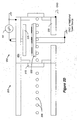
- Fig. 4A is a schematic illustrating major elements of a plasma processing chamber 400 implementing an embodiment of the invention.
- the chamber 400 includes a chamber body 422 and a chamber's ceiling 424 generally made of metal, such as aluminum, stainless steel, etc.
- a pedestal 408 is provided for supporting a carrier 420, upon which one or more substrates 402 are positioned.
- the shorthand carrier will be used to refer to various alternative elements such as, a removable susceptor; a tray, a substrate holder, etc. The point here is that the substrates are placed on the carrier and the carrier is placed on the pedestal and needs to make electrical contact thereto.
- the pedestal 408 may be attached to a lift mechanism 435, so that it is lowered for substrates loading via the valve 415, and then lifted up to the illustrated position for processing. Grounding is provided to the pedestal through the lift mechanism 435 and/or via, e.g., conductive electrical band or strap 401, depending on the size of the susceptor and the amount of power that needs to be delivered to the susceptor.
- the chamber has a cathode assembly 425 to which an RF power supply is coupled.
- ground potential is applied to the pedestal 408 so as to be coupled to the substrates.
- fixed grounding posts 430 are affixed to the pedestal 408, which in this embodiment serves as an electrode grounded by conductive band 401.
- the posts 430 are manually adjustable prior to operating the system in order to ensure edge contact and to cause the susceptor to conform to a desired profile.
- the carrier 420 is seated on the posts 430, such that electrical contact is made via the posts 430.
- the fixed posts 430 provide repeatable contact points for improved grounding.
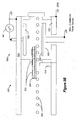
- Fig. 4B illustrates another embodiment of the invention.
- the elements of Fig. 4B are similar to those of Fig. 4A , except that resilient grounding contacts 438 are added in addition to the fixed posts 430.
- the top of the resilient grounding contacts 438 is extending above the top of the fixed posts 430.
- the carrier compresses the resilient contacts 438 until it rests on the posts 430. In this manner, good electrical contact is made through both the posts 430 and each of the resilient contacts 438.
- the fixed posts 430 may or may not be conductive, since electrical contact is ensured via the resilient contacts 438. Also, either the posts 430 or the resilient contacts 438 may be affixed to the carrier 420, rather than to the pedestal 408.
- a conductive spring 436 such as a leaf spring
- the block 432 is attached to the pedestal 408 by, e.g., bolt inserted through hole 434.
- the conductive springs form loaded electrical contact to ensure repeatable, reliable and multi-point connection to the carrier, whether it be a tray, or susceptor, etc., as show in Fig. 4C .
- This arrangement facilitates repeatable removal and placement of a try with substrates on the pedestal, or removal and placement of a susceptor on the pedestal. For example, the susceptor can be removed for cleaning, service, disposing of broken substrate, etc.
- the weight of the carrier compresses the spring 436 until the carrier rests on the fixed posts 430.
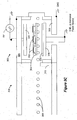
- Fig. 4D illustrates an example where no separate fixed posts are provided. Instead, a plurality of resilient contacts 438 are affixed to the pedestal or the floor of the chamber, and the carrier 420 rests directly on the springs 436.
- This embodiment may employ the resilient contacts 438 as described with reference to Fig.s 4B and 4C .
- this embodiment may employ a modified resilient contact that includes a stop 439.
- the spring 436 may be compressed by the weight of the carrier until the spring 436 contacts the stop 439. This limits the amount of compression of spring 436 and thereby fixes the elevation of the carrier 420.
- the chamber is provided with resilient contacts 438, wherein some of the resilient contacts 438 include stops, and the rest do not include a stop. For example, only the contacts 438 which are placed at the corners have stops, and the rest do not. According to another embodiment, all of the resilient contacts include stops.
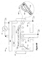
- Fig. 4E illustrates a top view of the chamber 400, wherein the carrier 420 is illustrated in broken line to indicate that it has been removed from the chamber.
- a relatively small number of posts 430 are provided, generally at the periphery of the pedestal.
- Large number resilient contacts 438 are distributed evenly throughout the area of the pedestal. That is, the number of resilient contacts is larger than the number of fixed posts, so that the fixed posts provide reliable and repeatable physical orientation, while the resilient contacts provide a reliable, repeatable, and distributed electrical contact.
- the carrier compresses the resilient contacts 438 to make good electrical contact, and then rests on the posts 430 that are on the periphery, thereby ensuring proper alignment.
- the posts 430 may include a conical top portion that may mate with a corresponding hole in the carrier to enhance the lateral and rotational alignment of the carrier.
- Fig. 4F illustrates another embodiment of a resilient contact 450.
- tubular section 454 is fixed, while sliding section 452 slides with respect to fixed section 454.
- sliding section 452 is shown as having a smaller diameter and slide inside the fixed section 454, however it may be constructed such that it has a larger diameter and slide over the fixed section 454.
- a spring 456 urges the sliding section 452 to an extended position.
- the resilient contact 450 includes a stop 458 that limits the compression of the sliding section 452.
- the fixed posts may be eliminated and instead several resilient contacts 450 with stops may be provided at the periphery or at the corners, while the remaining contacts may not have the stop.
- Fig. 4G is a top view of another embodiment of the chamber 400, wherein the carrier 420 is illustrated in broken line to indicate that it has been removed from the chamber.
- a relatively small number of posts 430 are provided.
- Large number resilient contacts 438 are distributed evenly about the periphery of the pedestal. That is, the resilient contacts 438 are closer to the edge of the carrier 420 than the fixed posts, so that the current leaves the carrier 420 at the edge through the springs 436 and never get to the posts 430.
- the fixed posts provide reliable and repeatable physical orientation, while the resilient contacts provide a reliable, repeatable, and distributed electrical contact.
- the carrier When the carrier is placed in the chamber, it compresses the resilient contacts 438 to make good electrical contact, and then rests on the posts 430 that are on the periphery, thereby ensuring proper alignment.
- the carrier compresses the resilient contacts 438 to make good electrical contact, and then rests on the posts 430 that are on the periphery, thereby ensuring proper alignment.
Landscapes
- Chemical & Material Sciences (AREA)
- Engineering & Computer Science (AREA)
- Physics & Mathematics (AREA)
- Plasma & Fusion (AREA)
- Organic Chemistry (AREA)
- General Chemical & Material Sciences (AREA)
- Chemical Kinetics & Catalysis (AREA)
- Materials Engineering (AREA)
- Mechanical Engineering (AREA)
- Metallurgy (AREA)
- Analytical Chemistry (AREA)
- Spectroscopy & Molecular Physics (AREA)
- Electromagnetism (AREA)
- Container, Conveyance, Adherence, Positioning, Of Wafer (AREA)
- Chemical Vapour Deposition (AREA)
- Drying Of Semiconductors (AREA)
- Plasma Technology (AREA)
Description
- The invention concerns a vacuum processing apparatus, such as plasma chambers used for etching or forming thin films on substrates or other workpieces.
- Manufacturing processes in the fields of semiconductor, flat panel displays, solar panels, etc., involve processing in vacuum chambers. For example, vacuum chambers are used for plasma-enhanced chemical vapor deposition (PECVD), physical vapor deposition (PVD), plasma etching and various other processes for forming thin films on substrates (workpieces) and etching structures on the substrates. In such chambers, various gases are flowed into the chamber, either via injectors or via a showerhead and plasma is ignited to etch or deposit thin film on the substrate. In order to attract charged species in the plasma towards the substrate, a ground potential is applied to the substrate or to an electrode under the substrate.
-
US 2010/136261 (A1) discloses a method and apparatus for processing substrates using plasma. More particularly, embodiments of the present invention provide a plasma processing chamber having an electrode coupled to a plurality of RF returning straps, wherein impedance of the RF returning straps are set and/or adjusted to tune the plasma distribution during processing. In one embodiment, impedance of RF returning straps varies by changing length of the RF returning straps, by changing width of the RF returning straps, by changing spacing of the RF returning straps, by changing location of the RF returning straps, by adding a capacitor to the RF returning straps, or by combinations thereof. -
WO2010091205 (A2 ) discloses a method and an apparatus for providing an electrically symmetrical ground or return path for electrical current between two electrodes is described. The apparatus includes at least on radio frequency (RF) device coupled to one of the electrodes and between a sidewall and/or a bottom of a processing chamber. The method includes moving one electrode relative to another and realizing a ground return path based on the position of the displaced electrode using one or both of a RF device coupled to a sidewall and the electrode, a RF device coupled to a bottom of the chamber and the electrode, or a combination thereof. -
Figs. 1A-1C are schematics of various stages of a vacuum processing chamber for processing one single substrate at a time, in which embodiments of the invention may-be implemented. Loadingchamber 105 is used to badsingle substrate 102 intovacuum processing chamber 100. InFig.1A , thevacuum door 115 is closed, and the substrate is positioned on the articulatedarm 111 ofrobot 110 in theloading chamber 105. As shown, thelower electrode 120, the chamber'sbody 122 and the chamber'sceiling 124 are all grounded. In this example, RF power is coupled to theupper electrode 125 while ground or other power is provided to thelower electrode 120. However, it is also known to couple ground to the upper electrode and supply RF power to the lower electrode or supply RF power to both the electrodes in a grounded chamber. - In
Fig. 1B , thevacuum door 115 has been opened, and the articulatedarm 111 introduces the substrate into the interior of theprocessing chamber 100. InFig. 1C , the substrate has been placed onto thesusceptor 120, the articulatedarm 111 has been retrieved, and thevacuum door 115 has been closed. In this condition plasma can be ignited and the processing can be carried out. Since the single substrate seats directly onto the susceptor, it generally conforms to irregularities on the susceptor and maintains good physical and uniform electrical contact with the susceptor. -
Figs. 2A-2D are schematics of various stages of a vacuum processing chamber for processing multiple substrate placed on a carrier, in which embodiments of the invention may be implemented. This embodiment is particularly suitable for fabricating solar cells on silicon wafers. It should be noted that while the illustrated embodiment shows a tray or carrier suitable for carrying several substrates simultaneously, the same can be done with a tray that is configured for carrying a single substrate. Loadingchamber 205 is used to loadseveral substrates 202, which are positioned on atray 204, intovacuum processing chamber 200. InFig. 2A , thevacuum door 215 is closed, and thesubstrates 202 are positioned on thetray 204, which may be delivered usingrollers 206, endless belt, etc. As shown, thelower electrode 220, the chamber'sbody 222 and the chamber'sceiling 224 are all grounded. In this example, RF power is coupled to theupper electrode 225 while ground or other power is provided to thelower electrode 220. However, it is also known to couple ground to the upper electrode and supply RF power to the lower electrode or supply RF power to both the electrodes in a grounded chamber. - In
Fig. 2B , thevacuum door 215 has been opened, and thetray 204 is introduced into the interior of theprocessing chamber 200. InFig. 2C , vacuum door has been closed and vacuum can be drawn inside thechamber 200. InFig. 2D thetray 204 been placed onto thesusceptor 220, which has been raised into its processing position. In this condition plasma can be ignited and the processing can be carried out. Since the single substrates do not seat directly on the susceptor, but are rather placed on a tray, and since the tray does not generally conform to irregularities on the susceptor, no uniform electrical-contact is being made to the susceptor. That is, the electrical path must pass from the susceptor to the tray and from the tray to each of the wafers. The tray or carrier does not fully conform to the susceptor and, consequently, electrical contact is not uniform and is rather limited to discrete points. -
Figs. 3A-3F are schematics of various stages of a vacuum processing chamber for processing multiple substrate placed on a susceptor, in which embodiments of the invention may be implemented. This embodiment is particularly suitable for fabricating solar cells, LED's, etc., on silicon wafers. It should be noted that while the illustrated embodiment shows a tray or carrier suitable for carrying several substrates simultaneously, the same can be done with a tray or carrier that is configured for carrying a single substrate. Loadingchamber 305 is used to loadseveral substrates 302, which are positioned on a tray orcarrier 304, intovacuum processing chamber 300. InFig. 3A , thevacuum door 315 is closed, and thesubstrates 302 are positioned on thetray 304, which may be delivered usingrollers 306, endless belt, etc. As shown, thelower electrode 320, the chamber'sbody 322 and the chamber'sceiling 324 are all grounded. In this example, RF power is coupled to theupper electrode 325 while ground or other power is provided to thelower electrode 320. In this embodiment the susceptor is seated onpedestal 308. However, it is also known to couple ground to the upper electrode and supply RF power to the tower electrode or supply RF power to both the electrodes in a grounded chamber. - In
Fig. 3B , thevacuum door 315 has been opened, and thetray 304 is introduced into the interior of theprocessing chamber 300. InFig. 3C , thetray 304 is completely within thechamber 300. InFig. 3D the susceptor is lifted and the substrates are transferred from the tray onto the susceptor. That is, the chamber ofFigs. 3A-3F includes atransfer mechanism 301 that is configured to transfer substrates from the tray onto the susceptor. InFig. 3E thetray 304 is removed from thechamber 300 and inFig. 3F thevacuum door 315 been closed and vacuum can be drawn inside thechamber 300. In this condition, plasma can be ignited and the processing can be carried out. In this embodiment, the electrical path must pass from the pedestal to the susceptor, and from the susceptor to each of the wafers. However, since the susceptor and the pedestal are not perfectly flat, the susceptor does not fully conform to the pedestal and, consequently, electrical contact is not uniform and is rather limited to discrete points. - For providing a reliable and repeatable multi-point electrical contact to the carrier, the vacuum processing chamber or the invention comprises the features of
claim 1. Preferred embodiments of the invention are characterized in the sub-claims. - A vacuum processing chambers having provisions for improved electrical contact to substrate carrier is disclosed. Specific embodiments provide a plasma processing chamber having a pedestal for supporting the carrier, and a plurality of fixed posts and resilient contacts are distributed over the area of the pedestal. The fixed posts provide physical support for the carrier, while the resilient contacts provide reliable and repeatable multi-point electrical contact to the carrier.
- Further advantages, features and potential applications of the present invention may be gathered from the description which follows, in conjunction with the embodiments illustrated in the drawings.
- Figs. 1A-1C
- are schematics of various stages of a vacuum processing chamber for processing one single substrate at a time, in which embodiments of the invention may be implemented.
- Figs. 2A-2D
- are schematics of various stages of a vacuum processing chamber for processing multiple substrate placed on a carrier, in which embodiments of the invention may be implemented.
- Figs. 3A-3F
- are schematics of various stages of a vacuum processing chamber for processing multiple substrate placed on a susceptor, in which embodiments of the invention may be implemented.
- Figs 4A-4D
- are schematics of vacuum processing chambers according to various embodiments of the invention.
- Fig. 4E
- illustrates a top view of the chamber according to an embodiment of the invention.
- Fig. 4F
- illustrates an alternative embodiment for the resilient contact.
- Fig. 4G
- is a top view of another embodiment of the chamber according to the invention.
-
Fig. 4A is a schematic illustrating major elements of aplasma processing chamber 400 implementing an embodiment of the invention. Thechamber 400 includes achamber body 422 and a chamber'sceiling 424 generally made of metal, such as aluminum, stainless steel, etc. Apedestal 408 is provided for supporting acarrier 420, upon which one ormore substrates 402 are positioned. Throughout the remaining of this description, the shorthand carrier will be used to refer to various alternative elements such as, a removable susceptor; a tray, a substrate holder, etc. The point here is that the substrates are placed on the carrier and the carrier is placed on the pedestal and needs to make electrical contact thereto. Thepedestal 408 may be attached to alift mechanism 435, so that it is lowered for substrates loading via thevalve 415, and then lifted up to the illustrated position for processing. Grounding is provided to the pedestal through thelift mechanism 435 and/or via, e.g., conductive electrical band orstrap 401, depending on the size of the susceptor and the amount of power that needs to be delivered to the susceptor. - At its top, the chamber has a
cathode assembly 425 to which an RF power supply is coupled. In the illustrated configuration, ground potential is applied to thepedestal 408 so as to be coupled to the substrates. In order to avoid the grounding problems mentioned above, in this embodiment, fixed groundingposts 430 are affixed to thepedestal 408, which in this embodiment serves as an electrode grounded byconductive band 401. In this respect, it should be appreciated that although during operation theposts 430 are fixed in a position, the post are manually adjustable prior to operating the system in order to ensure edge contact and to cause the susceptor to conform to a desired profile. Thecarrier 420 is seated on theposts 430, such that electrical contact is made via theposts 430. The fixedposts 430 provide repeatable contact points for improved grounding. However, such an arrangement may have very few reliable points of contact with thecarrier 420. This is especially the case when a tray is used, which is repeatedly removed and replaced inside the chamber. This is also the case for chambers where the susceptor is removable and is not bolted onto the pedestal. -
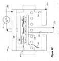
Fig. 4B illustrates another embodiment of the invention. The elements ofFig. 4B are similar to those ofFig. 4A , except thatresilient grounding contacts 438 are added in addition to the fixed posts 430. As shown, when no tray or susceptor is placed on the pedestal, the top of theresilient grounding contacts 438 is extending above the top of the fixed posts 430. As shown inFig. 4C , when acarrier 420 is placed on thepedestal 408, the carrier compresses theresilient contacts 438 until it rests on theposts 430. In this manner, good electrical contact is made through both theposts 430 and each of theresilient contacts 438. It should be appreciated however that in this embodiment the fixedposts 430 may or may not be conductive, since electrical contact is ensured via theresilient contacts 438. Also, either theposts 430 or theresilient contacts 438 may be affixed to thecarrier 420, rather than to thepedestal 408. - The callout in
Fig. 4B illustrates an example of aresilient contact 438. In this embodiment, aconductive spring 436, such as a leaf spring, is attached at one end to aconductive block 432. Theblock 432 is attached to thepedestal 408 by, e.g., bolt inserted throughhole 434. When severalresilient contacts 438 are secured to thepedestal 408, the conductive springs form loaded electrical contact to ensure repeatable, reliable and multi-point connection to the carrier, whether it be a tray, or susceptor, etc., as show inFig. 4C . This arrangement facilitates repeatable removal and placement of a try with substrates on the pedestal, or removal and placement of a susceptor on the pedestal. For example, the susceptor can be removed for cleaning, service, disposing of broken substrate, etc. As shown inFig. 4C , the weight of the carrier compresses thespring 436 until the carrier rests on the fixed posts 430. -
Fig. 4D illustrates an example where no separate fixed posts are provided. Instead, a plurality ofresilient contacts 438 are affixed to the pedestal or the floor of the chamber, and thecarrier 420 rests directly on thesprings 436. This embodiment may employ theresilient contacts 438 as described with reference toFig.s 4B and4C . On the other hand, as shown in the callout ofFig. 4D , this embodiment may employ a modified resilient contact that includes astop 439. As can be understood, thespring 436 may be compressed by the weight of the carrier until thespring 436 contacts thestop 439. This limits the amount of compression ofspring 436 and thereby fixes the elevation of thecarrier 420. According to one embodiment, the chamber is provided withresilient contacts 438, wherein some of theresilient contacts 438 include stops, and the rest do not include a stop. For example, only thecontacts 438 which are placed at the corners have stops, and the rest do not. According to another embodiment, all of the resilient contacts include stops. -
Fig. 4E illustrates a top view of thechamber 400, wherein thecarrier 420 is illustrated in broken line to indicate that it has been removed from the chamber. As shown, a relatively small number ofposts 430 are provided, generally at the periphery of the pedestal. Large numberresilient contacts 438 are distributed evenly throughout the area of the pedestal. That is, the number of resilient contacts is larger than the number of fixed posts, so that the fixed posts provide reliable and repeatable physical orientation, while the resilient contacts provide a reliable, repeatable, and distributed electrical contact. When the carrier is placed in the chamber, it compresses theresilient contacts 438 to make good electrical contact, and then rests on theposts 430 that are on the periphery, thereby ensuring proper alignment. As shown in the callout, theposts 430 may include a conical top portion that may mate with a corresponding hole in the carrier to enhance the lateral and rotational alignment of the carrier. -
Fig. 4F illustrates another embodiment of aresilient contact 450. InFig. 4F , tubular section 454 is fixed, while slidingsection 452 slides with respect to fixed section 454. InFig. 4F , slidingsection 452 is shown as having a smaller diameter and slide inside the fixed section 454, however it may be constructed such that it has a larger diameter and slide over the fixed section 454. Aspring 456 urges the slidingsection 452 to an extended position. When acarrier 420 is placed on the pedestal, the slidingsection 452 slides down and makes good electrical contact to thecarrier 420. According to one embodiment, optionally theresilient contact 450 includes astop 458 that limits the compression of the slidingsection 452. As explained before, using the stop option the fixed posts may be eliminated and instead severalresilient contacts 450 with stops may be provided at the periphery or at the corners, while the remaining contacts may not have the stop. -
Fig. 4G is a top view of another embodiment of thechamber 400, wherein thecarrier 420 is illustrated in broken line to indicate that it has been removed from the chamber. As shown, a relatively small number ofposts 430 are provided. Large numberresilient contacts 438 are distributed evenly about the periphery of the pedestal. That is, theresilient contacts 438 are closer to the edge of thecarrier 420 than the fixed posts, so that the current leaves thecarrier 420 at the edge through thesprings 436 and never get to theposts 430. The fixed posts provide reliable and repeatable physical orientation, while the resilient contacts provide a reliable, repeatable, and distributed electrical contact. When the carrier is placed in the chamber, it compresses theresilient contacts 438 to make good electrical contact, and then rests on theposts 430 that are on the periphery, thereby ensuring proper alignment. However, as discussed above and shown inFig. 4D , one may eliminate the fixed posts and rely on resilient posts only, or on resilient posts with stops. - While the invention has been described with reference to particular embodiments thereof, it is not limited to those embodiments. Specifically, various variations and modifications may be implemented by those of ordinary skill in the art without departing from the invention's scope, as defined by the appended claims.
-
- 100
- processing chamber
- 102
- single substrate
- 105
- loading chamber
- 110
- robot
- 111
- articulated arm
- 115
- vacuum door
- 120
- electrode, susceptor
- 122
- chamber's body
- 124
- chamber's ceiling
- 125
- upper electrode
- 200
- processing chamber
- 202
- substrates
- 204
- tray
- 205
- loading chamber
- 206
- rollers
- 215
- vacuum door
- 220
- electrode, susceptor
- 222
- chamber's body
- 224
- chamber's ceiling
- 225
- electrode
- 300
- processing chamber
- 301
- transfer mechanism
- 302
- substrates
- 304
- tray
- 305
- loading chamber
- 306
- rollers
- 308
- pedestal
- 315
- vacuum door
- 320
- electrode
- 322
- chamber's body
- 324
- chamber's ceiling
- 325
- electrode
- 400
- processing chamber
- 401
- band, strap
- 402
- substrates
- 408
- pedestal
- 415
- valve
- 420
- carrier
- 422
- chamber body
- 424
- chamber's ceiling
- 425
- cathode assembly
- 430
- posts
- 432
- block
- 434
- hole
- 435
- lift mechanism
- 436
- spring
- 438
- contacts
- 439
- stop
- 450
- contact
- 452
- sliding section
- 454
- fixed section
- 456
- spring
- 458
- stop
- RF
- power
Claims (14)
- A vacuum processing chamber, comprising:a chamber body (422);a pedestal (408) provided at a lower portion of the chamber body (422);a plurality of contacts (438, 450) provided on a top surface of the pedestal (408);a ground potential path coupling each of the contacts (438, 450) to ground potential;characterized in that:the contacts are resilient, anda substrate carrier (420) is seated on the pedestal (408), compresses the contacts (438, 450) and is making electrical contact to the contacts (438, 450).
- The vacuum processing chamber of claim 1, further characterized by a plurality of fixed posts (430) affixed to the top surface of the pedestal (408).
- The vacuum processing chamber of claim 2, characterized in that the plurality of fixed posts (430) are provided at periphery area of the pedestal (408) and the plurality of resilient contacts (438, 450) are distributed evenly over the area of the pedestal (408).
- The vacuum processing chamber of claim 1, characterized in that at least a portion of the plurality of resilient contacts (438, 450) comprises a stop (439, 458).
- The vacuum processing chamber of claim 1, characterized in that the plurality of resilient contacts (438, 450) are distributed about the periphery of the pedestal (408) and that the resilient contacts (438, 450) that are positioned at corners comprise stops (439, 458).
- The vacuum processing chamber of claim 1, characterized in that each of the resilient contacts (438) comprises a conductive block (432) and a leaf spring (436) attached at one end thereof to the conductive block (432).
- The vacuum processing chamber of claim 6, characterized in that each of the resilient contacts (438) further comprises a stop (439) provided between the conductive block (432) and the leaf spring (436).
- The vacuum processing chamber of claim 1, characterized in that each of the resilient contacts (450) comprises a fixed part (454) and a sliding part (452), and a spring (456) urging the sliding part (452) to an extended position.
- The vacuum processing chamber of any of claims 1 to 8, characterized in that the substrate carrier (420) comprises a susceptor configured for supporting a plurality of substrates simultaneously.
- The vacuum processing chamber of any of the claims 1 to 8, characterized in that the substrate carrier (420) comprises a substrate tray which is preferably configured for supporting a plurality of substrates.
- The vacuum processing chamber of any of the claims 1 to 12, characterized in that the substrate carrier (420) comprises one of a removable susceptor or a tray.
- The vacuum processing chamber of claim 11, further characterized by a transfer mechanism configured to transfer substrates from a tray onto the susceptor.
- The vacuum processing chamber for simultaneous plasma processing of a plurality of substrates positioned on a carrier (420) according to any of the claims 1 to 12, characterized by a showerhead provided at upper section of the chamber body (422).
- The vacuum processing chamber of any of the claims 1 to 13, characterized in that the plurality of resilient contacts (438, 450) are provided at a periphery area of the substrate carrier (420) and further comprising a plurality of fixed posts (430) on the top surface of the pedestal (408).
Applications Claiming Priority (1)
| Application Number | Priority Date | Filing Date | Title |
|---|---|---|---|
| US13/093,698 US20120267049A1 (en) | 2011-04-25 | 2011-04-25 | Grounding assembly for vacuum processing apparatus |
Publications (2)
| Publication Number | Publication Date |
|---|---|
| EP2518763A1 EP2518763A1 (en) | 2012-10-31 |
| EP2518763B1 true EP2518763B1 (en) | 2015-09-09 |
Family
ID=46168132
Family Applications (1)
| Application Number | Title | Priority Date | Filing Date |
|---|---|---|---|
| EP12165448.7A Active EP2518763B1 (en) | 2011-04-25 | 2012-04-25 | A grounding assembly for vacuum processing apparatus |
Country Status (6)
| Country | Link |
|---|---|
| US (1) | US20120267049A1 (en) |
| EP (1) | EP2518763B1 (en) |
| JP (1) | JP2012230900A (en) |
| KR (1) | KR102015657B1 (en) |
| CN (1) | CN102760631B (en) |
| TW (1) | TW201243982A (en) |
Cited By (3)
| Publication number | Priority date | Publication date | Assignee | Title |
|---|---|---|---|---|
| US9287152B2 (en) | 2009-12-10 | 2016-03-15 | Orbotech LT Solar, LLC. | Auto-sequencing multi-directional inline processing method |
| US9462921B2 (en) | 2011-05-24 | 2016-10-11 | Orbotech LT Solar, LLC. | Broken wafer recovery system |
| WO2021194702A1 (en) * | 2020-03-25 | 2021-09-30 | Applied Materials, Inc. | Rf return path for reduction of parasitic plasma |
Families Citing this family (8)
| Publication number | Priority date | Publication date | Assignee | Title |
|---|---|---|---|---|
| JP6348321B2 (en) * | 2013-05-17 | 2018-06-27 | キヤノンアネルバ株式会社 | Etching device |
| US10978334B2 (en) * | 2014-09-02 | 2021-04-13 | Applied Materials, Inc. | Sealing structure for workpiece to substrate bonding in a processing chamber |
| JP6440298B2 (en) * | 2014-09-04 | 2018-12-19 | 国立大学法人 新潟大学 | Plasma etching equipment |
| DE102015113962A1 (en) * | 2015-08-24 | 2017-03-02 | Meyer Burger (Germany) Ag | Substrate processing apparatus |
| US10923385B2 (en) * | 2016-11-03 | 2021-02-16 | Lam Research Corporation | Carrier plate for use in plasma processing systems |
| CN111326389B (en) * | 2018-12-17 | 2023-06-16 | 中微半导体设备(上海)股份有限公司 | Capacitively coupled plasma etching equipment |
| CN113972124B (en) * | 2020-07-23 | 2023-09-29 | 中微半导体设备(上海)股份有限公司 | Grounding assembly, plasma processing device and working method thereof |
| TW202306022A (en) * | 2021-06-18 | 2023-02-01 | 荷蘭商Asm Ip私人控股有限公司 | Vapor deposition assembly, susceptor treatment apparatus, and method of cleaning substrate |
Family Cites Families (9)
| Publication number | Priority date | Publication date | Assignee | Title |
|---|---|---|---|---|
| US6202589B1 (en) * | 1998-05-29 | 2001-03-20 | Advanced Micro Devices, Inc. | Grounding mechanism which maintains a low resistance electrical ground path between a plate electrode and an etch chamber |
| US6267839B1 (en) * | 1999-01-12 | 2001-07-31 | Applied Materials, Inc. | Electrostatic chuck with improved RF power distribution |
| JP4414072B2 (en) * | 2000-07-27 | 2010-02-10 | キヤノンアネルバ株式会社 | Tray for vacuum processing apparatus and vacuum processing apparatus |
| JP3886046B2 (en) * | 2002-12-18 | 2007-02-28 | シャープ株式会社 | Plasma CVD apparatus, film forming method using the same, and semiconductor device manufacturing method |
| US20100212832A1 (en) * | 2005-12-28 | 2010-08-26 | Sharp Kabushiki Kaisha | Stage device and plasma treatment apparatus |
| WO2010042860A2 (en) * | 2008-10-09 | 2010-04-15 | Applied Materials, Inc. | Rf return path for large plasma processing chamber |
| US20100136261A1 (en) * | 2008-12-03 | 2010-06-03 | Applied Materials, Inc. | Modulation of rf returning straps for uniformity control |
| TWI527930B (en) * | 2009-02-04 | 2016-04-01 | 應用材料股份有限公司 | Ground return path for plasma processing |
| KR101075842B1 (en) * | 2009-06-04 | 2011-10-25 | 주식회사 에스에프에이 | Inline type plasma processing apparatus for manufacturing solar cell |
-
2011
- 2011-04-25 US US13/093,698 patent/US20120267049A1/en not_active Abandoned
-
2012
- 2012-04-12 TW TW101112986A patent/TW201243982A/en unknown
- 2012-04-24 KR KR1020120042644A patent/KR102015657B1/en active Active
- 2012-04-24 JP JP2012098537A patent/JP2012230900A/en active Pending
- 2012-04-25 EP EP12165448.7A patent/EP2518763B1/en active Active
- 2012-04-25 CN CN201210124533.1A patent/CN102760631B/en not_active Expired - Fee Related
Cited By (4)
| Publication number | Priority date | Publication date | Assignee | Title |
|---|---|---|---|---|
| US9287152B2 (en) | 2009-12-10 | 2016-03-15 | Orbotech LT Solar, LLC. | Auto-sequencing multi-directional inline processing method |
| US9462921B2 (en) | 2011-05-24 | 2016-10-11 | Orbotech LT Solar, LLC. | Broken wafer recovery system |
| WO2021194702A1 (en) * | 2020-03-25 | 2021-09-30 | Applied Materials, Inc. | Rf return path for reduction of parasitic plasma |
| US11335543B2 (en) | 2020-03-25 | 2022-05-17 | Applied Materials, Inc. | RF return path for reduction of parasitic plasma |
Also Published As
| Publication number | Publication date |
|---|---|
| KR20120120909A (en) | 2012-11-02 |
| CN102760631B (en) | 2016-06-01 |
| EP2518763A1 (en) | 2012-10-31 |
| TW201243982A (en) | 2012-11-01 |
| CN102760631A (en) | 2012-10-31 |
| JP2012230900A (en) | 2012-11-22 |
| KR102015657B1 (en) | 2019-08-29 |
| US20120267049A1 (en) | 2012-10-25 |
Similar Documents
| Publication | Publication Date | Title |
|---|---|---|
| EP2518763A1 (en) | A grounding assembly for vacuum processing apparatus | |
| KR101641130B1 (en) | Rf return path for large plasma processing chamber | |
| US9343347B2 (en) | Portable electrostatic chuck carrier for thin substrates | |
| KR101155837B1 (en) | Edge ring arrangements for substrate processing | |
| US7375946B2 (en) | Method and apparatus for dechucking a substrate | |
| KR101593460B1 (en) | Ground return for plasma processes | |
| US20230059495A1 (en) | Optimization of Radiofrequency Signal Ground Return in Plasma Processing System | |
| US20130025790A1 (en) | Plasma processing apparatus and plasma processing method | |
| KR102735428B1 (en) | Substrate treating apparatus | |
| KR102739848B1 (en) | Grounding Strap Assemblies | |
| US10468221B2 (en) | Shadow frame with sides having a varied profile for improved deposition uniformity | |
| US10658159B2 (en) | Plasma reactor vessel having improved plasma uniformity comprised of a first electrode, a second electrode opposed to the first electrode, and a third electrode between a substrate carrier and the second electrode | |
| KR20170039876A (en) | Apparatus for processing substrate | |
| US12378669B2 (en) | Ground return for thin film formation using plasma | |
| CN121079752A (en) | Grounding device for forming thin film using plasma | |
| HK1222475B (en) | Plasma reactor vessel and assembly, and a method of performing plasma processing | |
| JP2009010018A (en) | Vertical substrate processing equipment | |
| JP2020501364A (en) | Substrate transfer device |
Legal Events
| Date | Code | Title | Description |
|---|---|---|---|
| PUAI | Public reference made under article 153(3) epc to a published international application that has entered the european phase |
Free format text: ORIGINAL CODE: 0009012 |
|
| AK | Designated contracting states |
Kind code of ref document: A1 Designated state(s): AL AT BE BG CH CY CZ DE DK EE ES FI FR GB GR HR HU IE IS IT LI LT LU LV MC MK MT NL NO PL PT RO RS SE SI SK SM TR |
|
| AX | Request for extension of the european patent |
Extension state: BA ME |
|
| 17P | Request for examination filed |
Effective date: 20130301 |
|
| GRAP | Despatch of communication of intention to grant a patent |
Free format text: ORIGINAL CODE: EPIDOSNIGR1 |
|
| INTG | Intention to grant announced |
Effective date: 20150106 |
|
| GRAS | Grant fee paid |
Free format text: ORIGINAL CODE: EPIDOSNIGR3 |
|
| GRAP | Despatch of communication of intention to grant a patent |
Free format text: ORIGINAL CODE: EPIDOSNIGR1 |
|
| INTG | Intention to grant announced |
Effective date: 20150710 |
|
| GRAA | (expected) grant |
Free format text: ORIGINAL CODE: 0009210 |
|
| AK | Designated contracting states |
Kind code of ref document: B1 Designated state(s): AL AT BE BG CH CY CZ DE DK EE ES FI FR GB GR HR HU IE IS IT LI LT LU LV MC MK MT NL NO PL PT RO RS SE SI SK SM TR |
|
| AX | Request for extension of the european patent |
Extension state: BA |
|
| REG | Reference to a national code |
Ref country code: GB Ref legal event code: FG4D |
|
| REG | Reference to a national code |
Ref country code: AT Ref legal event code: REF Ref document number: 748736 Country of ref document: AT Kind code of ref document: T Effective date: 20150915 Ref country code: CH Ref legal event code: EP |
|
| REG | Reference to a national code |
Ref country code: IE Ref legal event code: FG4D |
|
| REG | Reference to a national code |
Ref country code: DE Ref legal event code: R096 Ref document number: 602012010252 Country of ref document: DE |
|
| REG | Reference to a national code |
Ref country code: NL Ref legal event code: MP Effective date: 20150909 |
|
| PG25 | Lapsed in a contracting state [announced via postgrant information from national office to epo] |
Ref country code: NO Free format text: LAPSE BECAUSE OF FAILURE TO SUBMIT A TRANSLATION OF THE DESCRIPTION OR TO PAY THE FEE WITHIN THE PRESCRIBED TIME-LIMIT Effective date: 20151209 Ref country code: GR Free format text: LAPSE BECAUSE OF FAILURE TO SUBMIT A TRANSLATION OF THE DESCRIPTION OR TO PAY THE FEE WITHIN THE PRESCRIBED TIME-LIMIT Effective date: 20151210 Ref country code: LT Free format text: LAPSE BECAUSE OF FAILURE TO SUBMIT A TRANSLATION OF THE DESCRIPTION OR TO PAY THE FEE WITHIN THE PRESCRIBED TIME-LIMIT Effective date: 20150909 Ref country code: FI Free format text: LAPSE BECAUSE OF FAILURE TO SUBMIT A TRANSLATION OF THE DESCRIPTION OR TO PAY THE FEE WITHIN THE PRESCRIBED TIME-LIMIT Effective date: 20150909 Ref country code: LV Free format text: LAPSE BECAUSE OF FAILURE TO SUBMIT A TRANSLATION OF THE DESCRIPTION OR TO PAY THE FEE WITHIN THE PRESCRIBED TIME-LIMIT Effective date: 20150909 |
|
| REG | Reference to a national code |
Ref country code: LT Ref legal event code: MG4D |
|
| REG | Reference to a national code |
Ref country code: AT Ref legal event code: MK05 Ref document number: 748736 Country of ref document: AT Kind code of ref document: T Effective date: 20150909 |
|
| PG25 | Lapsed in a contracting state [announced via postgrant information from national office to epo] |
Ref country code: RS Free format text: LAPSE BECAUSE OF FAILURE TO SUBMIT A TRANSLATION OF THE DESCRIPTION OR TO PAY THE FEE WITHIN THE PRESCRIBED TIME-LIMIT Effective date: 20150909 Ref country code: ES Free format text: LAPSE BECAUSE OF FAILURE TO SUBMIT A TRANSLATION OF THE DESCRIPTION OR TO PAY THE FEE WITHIN THE PRESCRIBED TIME-LIMIT Effective date: 20150909 Ref country code: SE Free format text: LAPSE BECAUSE OF FAILURE TO SUBMIT A TRANSLATION OF THE DESCRIPTION OR TO PAY THE FEE WITHIN THE PRESCRIBED TIME-LIMIT Effective date: 20150909 Ref country code: HR Free format text: LAPSE BECAUSE OF FAILURE TO SUBMIT A TRANSLATION OF THE DESCRIPTION OR TO PAY THE FEE WITHIN THE PRESCRIBED TIME-LIMIT Effective date: 20150909 |
|
| REG | Reference to a national code |
Ref country code: FR Ref legal event code: PLFP Year of fee payment: 5 |
|
| PG25 | Lapsed in a contracting state [announced via postgrant information from national office to epo] |
Ref country code: NL Free format text: LAPSE BECAUSE OF FAILURE TO SUBMIT A TRANSLATION OF THE DESCRIPTION OR TO PAY THE FEE WITHIN THE PRESCRIBED TIME-LIMIT Effective date: 20150909 |
|
| PG25 | Lapsed in a contracting state [announced via postgrant information from national office to epo] |
Ref country code: EE Free format text: LAPSE BECAUSE OF FAILURE TO SUBMIT A TRANSLATION OF THE DESCRIPTION OR TO PAY THE FEE WITHIN THE PRESCRIBED TIME-LIMIT Effective date: 20150909 Ref country code: SK Free format text: LAPSE BECAUSE OF FAILURE TO SUBMIT A TRANSLATION OF THE DESCRIPTION OR TO PAY THE FEE WITHIN THE PRESCRIBED TIME-LIMIT Effective date: 20150909 Ref country code: CZ Free format text: LAPSE BECAUSE OF FAILURE TO SUBMIT A TRANSLATION OF THE DESCRIPTION OR TO PAY THE FEE WITHIN THE PRESCRIBED TIME-LIMIT Effective date: 20150909 Ref country code: IS Free format text: LAPSE BECAUSE OF FAILURE TO SUBMIT A TRANSLATION OF THE DESCRIPTION OR TO PAY THE FEE WITHIN THE PRESCRIBED TIME-LIMIT Effective date: 20160109 Ref country code: IT Free format text: LAPSE BECAUSE OF FAILURE TO SUBMIT A TRANSLATION OF THE DESCRIPTION OR TO PAY THE FEE WITHIN THE PRESCRIBED TIME-LIMIT Effective date: 20150909 |
|
| PG25 | Lapsed in a contracting state [announced via postgrant information from national office to epo] |
Ref country code: RO Free format text: LAPSE BECAUSE OF FAILURE TO SUBMIT A TRANSLATION OF THE DESCRIPTION OR TO PAY THE FEE WITHIN THE PRESCRIBED TIME-LIMIT Effective date: 20150909 Ref country code: PL Free format text: LAPSE BECAUSE OF FAILURE TO SUBMIT A TRANSLATION OF THE DESCRIPTION OR TO PAY THE FEE WITHIN THE PRESCRIBED TIME-LIMIT Effective date: 20150909 Ref country code: AT Free format text: LAPSE BECAUSE OF FAILURE TO SUBMIT A TRANSLATION OF THE DESCRIPTION OR TO PAY THE FEE WITHIN THE PRESCRIBED TIME-LIMIT Effective date: 20150909 Ref country code: PT Free format text: LAPSE BECAUSE OF FAILURE TO SUBMIT A TRANSLATION OF THE DESCRIPTION OR TO PAY THE FEE WITHIN THE PRESCRIBED TIME-LIMIT Effective date: 20160111 |
|
| REG | Reference to a national code |
Ref country code: DE Ref legal event code: R097 Ref document number: 602012010252 Country of ref document: DE |
|
| PLBE | No opposition filed within time limit |
Free format text: ORIGINAL CODE: 0009261 |
|
| STAA | Information on the status of an ep patent application or granted ep patent |
Free format text: STATUS: NO OPPOSITION FILED WITHIN TIME LIMIT |
|
| 26N | No opposition filed |
Effective date: 20160610 |
|
| PG25 | Lapsed in a contracting state [announced via postgrant information from national office to epo] |
Ref country code: DK Free format text: LAPSE BECAUSE OF FAILURE TO SUBMIT A TRANSLATION OF THE DESCRIPTION OR TO PAY THE FEE WITHIN THE PRESCRIBED TIME-LIMIT Effective date: 20150909 Ref country code: SI Free format text: LAPSE BECAUSE OF FAILURE TO SUBMIT A TRANSLATION OF THE DESCRIPTION OR TO PAY THE FEE WITHIN THE PRESCRIBED TIME-LIMIT Effective date: 20150909 Ref country code: BE Free format text: LAPSE BECAUSE OF NON-PAYMENT OF DUE FEES Effective date: 20160430 |
|
| REG | Reference to a national code |
Ref country code: CH Ref legal event code: PL |
|
| GBPC | Gb: european patent ceased through non-payment of renewal fee |
Effective date: 20160425 |
|
| PG25 | Lapsed in a contracting state [announced via postgrant information from national office to epo] |
Ref country code: LU Free format text: LAPSE BECAUSE OF FAILURE TO SUBMIT A TRANSLATION OF THE DESCRIPTION OR TO PAY THE FEE WITHIN THE PRESCRIBED TIME-LIMIT Effective date: 20160425 Ref country code: BE Free format text: LAPSE BECAUSE OF FAILURE TO SUBMIT A TRANSLATION OF THE DESCRIPTION OR TO PAY THE FEE WITHIN THE PRESCRIBED TIME-LIMIT Effective date: 20150909 |
|
| REG | Reference to a national code |
Ref country code: IE Ref legal event code: MM4A |
|
| PG25 | Lapsed in a contracting state [announced via postgrant information from national office to epo] |
Ref country code: GB Free format text: LAPSE BECAUSE OF NON-PAYMENT OF DUE FEES Effective date: 20160425 Ref country code: LI Free format text: LAPSE BECAUSE OF NON-PAYMENT OF DUE FEES Effective date: 20160430 Ref country code: CH Free format text: LAPSE BECAUSE OF NON-PAYMENT OF DUE FEES Effective date: 20160430 |
|
| REG | Reference to a national code |
Ref country code: FR Ref legal event code: PLFP Year of fee payment: 6 |
|
| PG25 | Lapsed in a contracting state [announced via postgrant information from national office to epo] |
Ref country code: IE Free format text: LAPSE BECAUSE OF NON-PAYMENT OF DUE FEES Effective date: 20160425 |
|
| REG | Reference to a national code |
Ref country code: FR Ref legal event code: PLFP Year of fee payment: 7 |
|
| PG25 | Lapsed in a contracting state [announced via postgrant information from national office to epo] |
Ref country code: SM Free format text: LAPSE BECAUSE OF FAILURE TO SUBMIT A TRANSLATION OF THE DESCRIPTION OR TO PAY THE FEE WITHIN THE PRESCRIBED TIME-LIMIT Effective date: 20150909 Ref country code: CY Free format text: LAPSE BECAUSE OF FAILURE TO SUBMIT A TRANSLATION OF THE DESCRIPTION OR TO PAY THE FEE WITHIN THE PRESCRIBED TIME-LIMIT Effective date: 20150909 Ref country code: HU Free format text: LAPSE BECAUSE OF FAILURE TO SUBMIT A TRANSLATION OF THE DESCRIPTION OR TO PAY THE FEE WITHIN THE PRESCRIBED TIME-LIMIT; INVALID AB INITIO Effective date: 20120425 |
|
| PG25 | Lapsed in a contracting state [announced via postgrant information from national office to epo] |
Ref country code: TR Free format text: LAPSE BECAUSE OF FAILURE TO SUBMIT A TRANSLATION OF THE DESCRIPTION OR TO PAY THE FEE WITHIN THE PRESCRIBED TIME-LIMIT Effective date: 20150909 Ref country code: MC Free format text: LAPSE BECAUSE OF FAILURE TO SUBMIT A TRANSLATION OF THE DESCRIPTION OR TO PAY THE FEE WITHIN THE PRESCRIBED TIME-LIMIT Effective date: 20150909 Ref country code: MK Free format text: LAPSE BECAUSE OF FAILURE TO SUBMIT A TRANSLATION OF THE DESCRIPTION OR TO PAY THE FEE WITHIN THE PRESCRIBED TIME-LIMIT Effective date: 20150909 Ref country code: MT Free format text: LAPSE BECAUSE OF NON-PAYMENT OF DUE FEES Effective date: 20160430 |
|
| PG25 | Lapsed in a contracting state [announced via postgrant information from national office to epo] |
Ref country code: BG Free format text: LAPSE BECAUSE OF FAILURE TO SUBMIT A TRANSLATION OF THE DESCRIPTION OR TO PAY THE FEE WITHIN THE PRESCRIBED TIME-LIMIT Effective date: 20150909 |
|
| PG25 | Lapsed in a contracting state [announced via postgrant information from national office to epo] |
Ref country code: AL Free format text: LAPSE BECAUSE OF FAILURE TO SUBMIT A TRANSLATION OF THE DESCRIPTION OR TO PAY THE FEE WITHIN THE PRESCRIBED TIME-LIMIT Effective date: 20150909 |
|
| PGFP | Annual fee paid to national office [announced via postgrant information from national office to epo] |
Ref country code: FR Payment date: 20220425 Year of fee payment: 11 Ref country code: DE Payment date: 20220427 Year of fee payment: 11 |
|
| REG | Reference to a national code |
Ref country code: DE Ref legal event code: R081 Ref document number: 602012010252 Country of ref document: DE Owner name: KLA CORPORATION, MILPITAS, US Free format text: FORMER OWNER: ORBOTECH LT SOLAR, LLC, SAN JOSE, CALIF., US Ref country code: DE Ref legal event code: R082 Ref document number: 602012010252 Country of ref document: DE Representative=s name: REICHERT & LINDNER PARTNERSCHAFT PATENTANWAELT, DE |
|
| P01 | Opt-out of the competence of the unified patent court (upc) registered |
Effective date: 20230525 |
|
| REG | Reference to a national code |
Ref country code: DE Ref legal event code: R119 Ref document number: 602012010252 Country of ref document: DE |
|
| PG25 | Lapsed in a contracting state [announced via postgrant information from national office to epo] |
Ref country code: FR Free format text: LAPSE BECAUSE OF NON-PAYMENT OF DUE FEES Effective date: 20230430 Ref country code: DE Free format text: LAPSE BECAUSE OF NON-PAYMENT OF DUE FEES Effective date: 20231103 |