EP2517112B1 - Mechanismus zur erkennung eines nicht erfolgten prozessoraustauschs und zur änderung einer hochgeschwindigkeits-buskalibrierung während des hochfahrens - Google Patents
Mechanismus zur erkennung eines nicht erfolgten prozessoraustauschs und zur änderung einer hochgeschwindigkeits-buskalibrierung während des hochfahrens Download PDFInfo
- Publication number
- EP2517112B1 EP2517112B1 EP10842409.4A EP10842409A EP2517112B1 EP 2517112 B1 EP2517112 B1 EP 2517112B1 EP 10842409 A EP10842409 A EP 10842409A EP 2517112 B1 EP2517112 B1 EP 2517112B1
- Authority
- EP
- European Patent Office
- Prior art keywords
- identifier
- identifiers
- processor
- memory
- match
- Prior art date
- Legal status (The legal status is an assumption and is not a legal conclusion. Google has not performed a legal analysis and makes no representation as to the accuracy of the status listed.)
- Active
Links
Images


Classifications
-
- G—PHYSICS
- G06—COMPUTING OR CALCULATING; COUNTING
- G06F—ELECTRIC DIGITAL DATA PROCESSING
- G06F21/00—Security arrangements for protecting computers, components thereof, programs or data against unauthorised activity
- G06F21/70—Protecting specific internal or peripheral components, in which the protection of a component leads to protection of the entire computer
- G06F21/71—Protecting specific internal or peripheral components, in which the protection of a component leads to protection of the entire computer to assure secure computing or processing of information
- G06F21/74—Protecting specific internal or peripheral components, in which the protection of a component leads to protection of the entire computer to assure secure computing or processing of information operating in dual or compartmented mode, i.e. at least one secure mode
-
- G—PHYSICS
- G06—COMPUTING OR CALCULATING; COUNTING
- G06F—ELECTRIC DIGITAL DATA PROCESSING
- G06F21/00—Security arrangements for protecting computers, components thereof, programs or data against unauthorised activity
- G06F21/30—Authentication, i.e. establishing the identity or authorisation of security principals
- G06F21/44—Program or device authentication
-
- G—PHYSICS
- G06—COMPUTING OR CALCULATING; COUNTING
- G06F—ELECTRIC DIGITAL DATA PROCESSING
- G06F21/00—Security arrangements for protecting computers, components thereof, programs or data against unauthorised activity
- G06F21/50—Monitoring users, programs or devices to maintain the integrity of platforms, e.g. of processors, firmware or operating systems
- G06F21/57—Certifying or maintaining trusted computer platforms, e.g. secure boots or power-downs, version controls, system software checks, secure updates or assessing vulnerabilities
- G06F21/575—Secure boot
-
- G—PHYSICS
- G06—COMPUTING OR CALCULATING; COUNTING
- G06F—ELECTRIC DIGITAL DATA PROCESSING
- G06F21/00—Security arrangements for protecting computers, components thereof, programs or data against unauthorised activity
- G06F21/70—Protecting specific internal or peripheral components, in which the protection of a component leads to protection of the entire computer
- G06F21/71—Protecting specific internal or peripheral components, in which the protection of a component leads to protection of the entire computer to assure secure computing or processing of information
- G06F21/73—Protecting specific internal or peripheral components, in which the protection of a component leads to protection of the entire computer to assure secure computing or processing of information by creating or determining hardware identification, e.g. serial numbers
-
- G—PHYSICS
- G06—COMPUTING OR CALCULATING; COUNTING
- G06F—ELECTRIC DIGITAL DATA PROCESSING
- G06F21/00—Security arrangements for protecting computers, components thereof, programs or data against unauthorised activity
- G06F21/70—Protecting specific internal or peripheral components, in which the protection of a component leads to protection of the entire computer
- G06F21/82—Protecting input, output or interconnection devices
- G06F21/85—Protecting input, output or interconnection devices interconnection devices, e.g. bus-connected or in-line devices
-
- G—PHYSICS
- G06—COMPUTING OR CALCULATING; COUNTING
- G06F—ELECTRIC DIGITAL DATA PROCESSING
- G06F9/00—Arrangements for program control, e.g. control units
- G06F9/06—Arrangements for program control, e.g. control units using stored programs, i.e. using an internal store of processing equipment to receive or retain programs
- G06F9/44—Arrangements for executing specific programs
- G06F9/4401—Bootstrapping
- G06F9/4403—Processor initialisation
-
- G—PHYSICS
- G06—COMPUTING OR CALCULATING; COUNTING
- G06F—ELECTRIC DIGITAL DATA PROCESSING
- G06F2221/00—Indexing scheme relating to security arrangements for protecting computers, components thereof, programs or data against unauthorised activity
- G06F2221/21—Indexing scheme relating to G06F21/00 and subgroups addressing additional information or applications relating to security arrangements for protecting computers, components thereof, programs or data against unauthorised activity
- G06F2221/2105—Dual mode as a secondary aspect
-
- G—PHYSICS
- G06—COMPUTING OR CALCULATING; COUNTING
- G06F—ELECTRIC DIGITAL DATA PROCESSING
- G06F2221/00—Indexing scheme relating to security arrangements for protecting computers, components thereof, programs or data against unauthorised activity
- G06F2221/21—Indexing scheme relating to G06F21/00 and subgroups addressing additional information or applications relating to security arrangements for protecting computers, components thereof, programs or data against unauthorised activity
- G06F2221/2129—Authenticate client device independently of the user
-
- G—PHYSICS
- G06—COMPUTING OR CALCULATING; COUNTING
- G06F—ELECTRIC DIGITAL DATA PROCESSING
- G06F2221/00—Indexing scheme relating to security arrangements for protecting computers, components thereof, programs or data against unauthorised activity
- G06F2221/21—Indexing scheme relating to G06F21/00 and subgroups addressing additional information or applications relating to security arrangements for protecting computers, components thereof, programs or data against unauthorised activity
- G06F2221/2149—Restricted operating environment
-
- G—PHYSICS
- G06—COMPUTING OR CALCULATING; COUNTING
- G06F—ELECTRIC DIGITAL DATA PROCESSING
- G06F2221/00—Indexing scheme relating to security arrangements for protecting computers, components thereof, programs or data against unauthorised activity
- G06F2221/21—Indexing scheme relating to G06F21/00 and subgroups addressing additional information or applications relating to security arrangements for protecting computers, components thereof, programs or data against unauthorised activity
- G06F2221/2153—Using hardware token as a secondary aspect
Definitions
- Embodiments of the invention relate to high frequency bus calibration techniques. More particularly, embodiments of the invention relate to mechanisms to determine whether a processor or processor core has been removed from a host platform and modification of high frequency channel calibration during boot based on the determination.
- DRAM dynamic random access memory
- DIMM dual inline memory modules
- DIMMs DIMMs per channel and other optimizations.
- multi-socket system performance improvements require faster and better interconnects between the processors.
- DDR training includes many time consuming steps, for example, centering of various strobe signals, cross talk elimination and reference voltage calibration. These calibration steps are used to derive optimal DDR timing parameters that are applied to the DRAM controller and DIMMs. This programming is done before memory is accessed as these parameters cannot be updated during operation without disturbing memory traffic.
- Non-optimum parameters result in higher bit error rates and generally destabilize system operation. These complex calibration steps result in increased boot time.
- Current DDR-4 proposals call for per DDR device calibration across multiple parameters to achieve higher speeds and lower voltages. As a result, memory training processes in these platforms may be increased.
- BIOS may eliminate some or all DDR training steps from most boot cycles and allow improved time to video metrics.
- DDR training parameters are function of electrical characteristics of memory DIMMs, processor(s) and DRAM channel(s). The training steps can be skipped if the BIOS can determine that the DIMMs and processor have not changed on the motherboard since the last boot.
- Memory DIMMs are required to contain a serial number for tracking purposes and most motherboards contain a serial number such as Wired for Management (WfM) Globally Unique Identifier (GUID).
- WfM Wired for Management
- GUID Globally Unique Identifier
- Some platforms may place additional components (e.g. buffers) or cards in the memory channel path. These components or memory cards plugged into the connectors can also carry a serial number. As a result, the BIOS can track memory DIMMs, buffers, and motherboard and memory cards.
- BIOS can track the processor. Even if the processors have a serial number, for example, for manufacturing tracking purposes, this serial number is generally not exposed to BIOS due to privacy/security concerns. Described herein are techniques that allow the BIOS to utilize the serial number of a processor without violating privacy/security requirements. Some systems may have other components with similar privacy requirements and solutions proposed here can be extended to handle those components.
- processor swapping is rare, but lack of a detection mechanism requires the BIOS to operate on worst case assumptions and perform calibration procedures each time the system is booted up.
- the detection mechanisms described herein may allow the BIOS to eliminate DDR training for most boot processes and provide faster boot times and faster time to video times.
- the processor identification mechanism utilizes an Intel® Trusted eXecution Technology (TXT) AC Module (ACM) and Intel® TXT hardware to determine the serial number for processor(s) of the host platform.
- the ACM is a binary module that is delivered and cryptographically signed by the manufacturer (e.g., Intel®).
- the processor authenticates the ACM prior to launch using a public key embedded in the chipset.
- the ACM is executed from within the processor cache and is protected from modifications and snooping during execution.
- the ACM has higher privileges than BIOS or ordinary software and can be considered a logical extension of processor microcode.
- the processor microcode has the ability to detect whether a processor is in AC Mode or not. Currently, this capability is used by processor microcode to expose TXT-privileged operations (e.g., unlock memory) to the ACM via a machine state register (MSR) interface.
- MSR machine state register
- the mechanisms described herein utilize an ACM-only MSR (e.g., PSN_ACM_MSR) that exposes the processor serial number information to the ACM only.
- PSN_ACM_MSR general protection fault
- a Trusted Platform Module may be utilized.
- the TPM provides non-volatile (NV) storage for cryptographic operations.
- the TPM is soldered on the motherboard and is thus physically tied to the platform.
- the TPM supports multiple privilege levels known as "locality.”
- the ACM has access to locality 3. Ordinary software including BIOS and the host operating system (OS), does not have access to this locality.
- the ACM uses locality 3 NV storage to store parameters that need to be protected from BIOS and the OS.
- the ACM can store the processor serial number(s) obtained by reading the MSR in locality 3 NV storage.
- the ACM provides a MatchCPU() function that can be invoked by the BIOS. When this function is invoked, the ACM can read the CPU MSR through, for example, PSN_ACM_MSR and compare it with serial numbers stored in TPM NV memory. If the serial numbers match, the ACM can return success indicating no processor swap has occurred.
- the BIOS can repeat this procedure for each processor. Because the comparison is performed by the ACM, the serial number is not exposed to the software that invokes the ACM, which satisfies many privacy/security guidelines. If the BIOS can determine, through this process, that the processor(s) and DIMMs have not changed since the last calibration process, the BIOS can skip the DDR calibration process.
- MP multi-processor
- platform software can disable one or more processor cores in a processor based on, for example, failure history. When such a processor is replaced by a new processor, the platform software is expected to re-enable the replaced processor core(s).
- the techniques described herein may be utilized to determine when the processor core(s) have been replaced. Other uses of these mechanisms can also be provided.
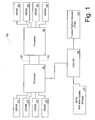
- Figure 1 is a block diagram of one embodiment of an electronic system in which a mechanism may be provided to detect a processor identifier change that utilizes an ACM, but does not expose the identifier to general purpose software.
- the example of Figure 1 includes two processors; however, the techniques described herein are equally applicable to single processor systems as well as systems with more then two processors.
- the non-memory components i.e., processors, chipset, TPM, BIOS
- components that are compatible with the Intel Architecture may be utilized.
- processors that provide security to processor identifiers may be utilized.
- BIOS 120 may begin the initialization or boot up process. While the boot up process may include many functions, one aspect is the calibration of memory channels.
- processors 160 and 180 support TXT or a similar level of security. Processors 160 and 180 are coupled to BIOS 120 and Trusted Platform Module (TPM) 140 via chip set 130. In one embodiment, processor 180 is coupled with chip set 130 via processor 160. Processor 160 and processor 180 may be interconnected with various interconnection protocols, for example, QPI.
- processor 160 is coupled with dynamic random access memories (DRAMs) 172, 174, 176 and 178 and processor 180 is coupled with DRAMs 192, 194, 196 and 198.
- DRAMs dynamic random access memories
- the channels between processors 160 and 180 and DRAMs 172, 174, 176, 178, 192, 194, 196 and 198 are Double Data Rate (DDR) and can be any generation of DDR memory channel (e.g., DDR1, DDR2, DDR3, DDR4).
- DDR Double Data Rate
- the ACM is transferred from BIOS 120 through chip set 130 to processor 160 for execution.
- ACM execution occurs within the TXT environment of processor 160.
- the ACM may determine the identifier (e.g., serial number) of processor 160 and/or processor 180.
- the ACM request for the processor identifier occurs within the TXT environment and requests that the identifier be returned to an ACM-only register. As a result, the identifier remains within the secure TXT environment and remains shielded from general purpose software.
- TPM 140 may store a copy of a processor identifier from a previous boot process. The copy stored by TPM 140 may be used for comparison purposes for the current boot process.
- the protected channel is opened and closed by micocode executed by processor 160.
- the results of the comparison are utilized by the ACM and BIOS 120 to determine whether to perform a full boot up that includes memory channel calibration process. That is, if the processor identifiers match, the ACM and/or BIOS 120 may skip the memory channel calibration process. If the processor identifiers do not match, the new processor identifier may be stored in TPM 140 and the memory channel calibration process may be performed.
- processor identifiers may be for the interconnection(s) between processor 160 and processor 180. If the processor identifiers for both processor 160 and 180 match the previous boot up, calibration of links 150 and 155 may be skipped. If one of the processor identifiers for processor 160 or processor 180 does not match the previous boot up, calibration links 150 and 155 may be performed.
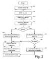
- Figure 2 is a flow diagram of one embodiment of a boot process may utilize a processor identifier to determine whether to perform memory channel calibration as part of a boot process.
- the boot process of Figure 2 may be applied to a system such as the system of Figure 1 .
- the system is powered up, 200.
- the BIOS of the system gains control of the system, 205.
- the BIOS manages the boot up process of the host system.
- the platform identifier is determined, 210.
- the platform identifier is not a secure identifier and can be determined in any manner known in the art.
- each DRAM chip has an identifier that is not secure.
- the memory identifiers can be determined in any manner known in the art. The system can then determine wither the gathered identifiers match with previously stored identifiers, 225.
- the memory identifiers are saved in a non-volatile memory for a subsequent boot process, 250.
- a full memory calibration is performed, 255.
- the memory calibration parameters are saved, 260, and the boot process continues, 270.
- processor identifier matching is invoked, 230.
- processor identifier matching is successful, 235, the stored memory calibration parameters are utilized, 240. If processor identifier matching is not successful, 235, memory calibration is performed, 255. The memory calibration parameters are saved, 260, and the boot process continues, 270.
- Figure 3 is a flow diagram of one embodiment of a process to determine a processor identifier in a secure manner.
- the process of Figure 3 can be called by BIOS using TXT instructions, which instruct the microcode to launch ACM inside a shielded environment.
- the processor identifier(s) are read securely, 300. In one embodiment, this may be accomplished by secure microcode operations that retrieve the processor identifier(s) and utilize an ACM-only machine specific register a.k.a. MSR (e.g., PSN_ACM_MSR) that exposes the processor serial number information to the ACM only.
- a.k.a. MSR e.g., PSN_ACM_MSR
- the processor identifier(s) from the previous boot is read from memory that is shielded from general purpose software, 310.
- the previous processor identifier(s) are stored in a Locality 3 non-volatile memory in a TPM.
- other secure mechanisms may be utilized to store the processor identifier(s).
- the processor identifiers from the current boot operation and compared to the stored processor identifier(s), 320.
- processor identifier(s) match, 320, a SUCCESS indication is returned to the calling function, 330. If the processor identifier(s) do not match, 320, the new processor identifier(s) are saved in a secure storage, 340. In one embodiment, the processor identifier(s) are stored in a Locality 3 non-volatile storage. A FAILURE indication is then returned to the calling function, 350. In no case, the calling function, which is part of BIOS, learns about the actual processor identifiers.
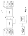
- FIG 4 is a block diagram of one embodiment of an electronic system in which a mechanism may be provided to determine a processor identifier securely utilizing an Intel Manageability Engine (ME). Platforms that do not support TXT or may not contain TPM, can benefit from using this alternate ME based solution.
- the ME executes firmware that is delivered and cryptographically signed by its manufacturer (e.g., Intel Corporation).
- BIOS 420 may begin the initialization or boot up process. While the boot up process may include many functions, one aspect is the calibration of memory channels.
- processors 460 and 480 support TXT or a similar level of security.
- Processors 460 and 480 are coupled to BIOS 420 via chip set 430, which includes ME 435.
- processor 480 is coupled with chip set 430 via processor 460.
- Processor 460 and processor 480 may be interconnected with various interconnection protocols, for example, QPI.
- processor 460 is coupled with dynamic random access memories (DRAMs) 472, 474, 476 and 478 and processor 480 is coupled with DRAMs 492, 494, 496 and 498.
- DRAMs dynamic random access memories
- the channels between processors 460 and 480 and DRAMs 472, 474, 476, 478, 492, 494, 496 and 498 can be any generation of DDR memory channel (e.g., DDR1, DDR2, DDR3, DDR4).
- chipset 430 authenticates ME firmware 435 using a public key embedded in chipset 430, prior to launch.
- ME firmware 435 may be authenticated in a different manner.
- ME firmware runs in a ME execution environment inside chipset 430 and is protected from modifications and snooping by host software.
- ME firmware 435 has a secure path to processor 460 through chipset 430 and uses the secure path to obtain processor identifier(s), PSN.
- the ME subsystem contains a Random Number Generator.
- ME firmware 435 can use this facility to create a random number R.
- ME firmware 435 can compute hash of R and PSN, H.
- H Hash (R, PSN) where Hash function represents a standard algorithm, for example, SHA-2.
- ME firmware 435 stores R and H in a non-volatile memory.
- PSN is not directly stored in the non-volatile memory.
- Software can read the non-volatile memory contents and determine R and H. However, it is computationally infeasible to calculate PSN based on R and H since Hash functions are a one way functions.
- processor identifiers may be for the interconnection(s) between processor 460 and processor 480. If the processor identifiers for both processor 460 and 480 match the previous boot up, calibration of links 450 and 455 may be skipped. If one of the processor identifiers for processor 460 or processor 480 does not match the previous boot up, calibration links 450 and 455 may be performed.
- FIG. 5 is a flow diagram of one embodiment of a technique for comparing processor identifier(s) utilizing a Manageability Engine.
- the processor identifier(s) are determined via a secure interface, 510.
- the values of R and H are retrieved from memory, 520.
- a hash value, H1 is determined using the current R and processor identifier(s), PSN, 530.
- the computed hash value, H1 is compared to the stored hash value, H, 540. If H and H1 are equal, 540, a SUCCESS indication is returned, 550. If the computed hash value, H1, and H are not equal, 540, the computed has value, H1, is stored in the secure memory, 560. A FAILURE indication is then returned, 570.
Landscapes
- Engineering & Computer Science (AREA)
- Theoretical Computer Science (AREA)
- Computer Hardware Design (AREA)
- Software Systems (AREA)
- Physics & Mathematics (AREA)
- Computer Security & Cryptography (AREA)
- General Engineering & Computer Science (AREA)
- General Physics & Mathematics (AREA)
- Mathematical Physics (AREA)
- Stored Programmes (AREA)
- Storage Device Security (AREA)
Claims (13)
- Verfahren, aufweisend:Bestimmen (220) von Kennungen für mehrere Speichervorrichtungen (472, 474, 476, 478, 492, 494, 496, 498) in einem elektronischen Hostsystem (400) als Reaktion auf einen eingeschalteten Zustand (200);Durchführen (255) einer Speicherkanalkalibrierung, wenn die Kennungen nicht mit Kennungen aus einem vorangehenden Hochfahren (225) übereinstimmen;Bestimmen (230) einer Kennung eines Prozessors oder mehrerer Prozessoren (460, 480) des elektronischen Hostsystems (400), wenn die Kennungen mit Kennungen aus einem vorangehenden Hochfahren übereinstimmen, über einen sicheren Prozess (225);Vollenden (270) des Hochfahrprozesses ohne Kalibrierung von Speicherkanälen (240), wenn die Speicherkennungen und die Prozessorkennung mit Speicherkennungen aus einem vorangehenden Hochfahrprozess und Prozessorkennungen aus dem vorangehenden Hochfahrprozess übereinstimmen (235).
- Verfahren nach Anspruch 1, des Weiteren aufweisend:Bestimmen einer Kennung einer Hauptplatine des elektronischen Hostsystems (400) undDurchführen einer Speicherkanalkalibrierung, wenn die Kennungen für die Speichervorrichtungen oder die Kennung für die Hauptplatine nicht mit entsprechenden Kennungen aus einem vorangehenden Hochfahren übereinstimmen.
- Verfahren nach Anspruch 1, wobei das Bestimmen der Kennung einer Hauptplatine des elektronischen Hostsystems (400) ein Bestimmen einer laufenden Nummer für die Hauptplatine aufweist.
- Verfahren nach Anspruch 1, wobei das Bestimmen von Kennungen für die mehreren Speichervorrichtungen im elektronischen Hostsystem (400) als Reaktion auf einen eingeschalteten Zustand ein Bestimmen einer laufenden Nummer für jede integrierte, dynamische Speicherschaltung mit wahlfreiem Zugriff (Dynamic Random Access Memory - DRAM) im elektronischen Hostsystem aufweist.
- Verfahren nach Anspruch 1, wobei das Bestimmen, ob die Kennung eines Prozessors oder mehrerer Prozessoren (160, 180) des elektronischen Hostsystems (400) mit Kennungen aus dem vorangehenden Hochfahren übereinstimmen, ohne die Kennungen einer Allzweck-Software auszusetzen, aufweist:Aufrufen einer geschützten Funktion, die die Kennung eines Prozessors oder mehrerer Prozessoren innerhalb eines abgeschirmten Kontexts abfragt;Vergleichen, innerhalb des abgeschirmten Kontexts, der abgefragten Kennung mit einer Kennung eines Prozessors oder mehrerer Prozessoren aus dem vorangehenden Hochfahren, wobei die Kennung aus dem vorangehenden Hochfahren an einer geschützten Speicherstelle gespeichert ist;Rücksenden einer Erfolgsanzeige, wenn die Kennungen übereinstimmen; undRücksenden einer Ausfallsanzeige, wenn die Kennungen nicht übereinstimmen.
- Verfahren nach Anspruch 5, wobei das Aufrufen der geschützten Funktion zum Erkennen einer Änderung in einer Kennung eines Prozessors oder mehrerer Prozessoren (160, 180) aufweist:Abrufen einer AC-Modul- (ACM) Funktion, die die Kennung innerhalb eines ACM-Kontexts liest und die Kennung zu einem geschützten Register zurücksendet;Vergleich der Kennung, die im geschützten Register gespeichert ist, mit der Kennung aus dem vorangehenden Hochfahren, die an einer geschützten Speicherstelle in einem sicheren Modul im elektronischen Hostsystem gespeichert ist, wobei die Kennungen über geschützte Kanäle gesendet werden;wobei die Kennungen niemals einer Allzweckumgebung ausgesetzt sind.
- Verfahren nach Anspruch 5, wobei das Aufrufen der geschützten Funktion zum Abfragen der Kennung eines Prozessors oder mehrerer Prozessoren (160, 180) aufweist:Lesen der Kennung innerhalb einer abgeschirmten Umgebung;Erstellen eines Hash-Wertes für die Kennung;Abfragen eines Hash-Wertes für die Kennung aus dem vorangehenden Hochfahren;Vergleichen der Hash-Werte;wobei die Kennungen niemals einer Allzweckumgebung ausgesetzt sind.
- Artikel, aufweisend eine Speichervorrichtung (472, 474, 476, 478, 492, 494, 496, 498), die in einem elektronischen Hostsystem (400) eingebettet ist, in der Anweisungen gespeichert sind, die, wenn sie ausgeführt werden, eine oder mehrere Komponente(n) eines elektronischen Hostsystems veranlassen, das Verfahren nach einem der Ansprüche 1 bis 7 auszuführen.
- System (100), aufweisend:einen Prozessor (160, 180) zum selektiven Ausführen von Speicherkanalkalibrierungsoperationen;eine oder mehrere Speichervorrichtung(en) (472, 474, 476, 478, 492, 494, 496, 498), die über entsprechende Speicherkanäle mit dem Prozessor gekoppelt sind;einen Chipsatz, der mit dem Prozessor (160, 180) gekoppelt ist;ein Eingabe/Ausgabe-Basissystem (Basic Input/Output System - BIOS) (420), das mit dem Chipsatz gekoppelt ist, wobei als Reaktion auf einen eingeschalteten Zustand (200) zum Einleiten eines aktuellen Hochfahrprozesses (205) das BIOS Kennungen für mehrere Speichervorrichtung in einem elektronischen Hostsystem (400) als Reaktion auf einen eingeschalteten Zustand (200) bestimmt (220), veranlasst, dass Speicherkanalkalibrierungsoperationen (255) vom Prozessor (160, 180) ausgeführt werden, wenn die Kennungen nicht mit Kennungen aus einem vorangehenden Hochfahren (225) übereinstimmen, wobei das BIOS ferner eine Kennung des Prozessors über einen sicheren Prozess bestimmt (230), wenn die Kennungen mit Kennungen aus dem vorangehenden Hochfahren übereinstimmen (235), wobei das BIOS den aktuellen Hochfahrprozess ohne Speicherkanäle zu kalibrieren beendet (270), wenn die Speicherkennungen (240) und die Prozessorkennung mit Speicherkennungen aus einem vorangehenden Hochfahrprozess und Prozessorkennungen aus dem vorangehenden Hochfahrprozess (235) übereinstimmen.
- System (100) nach Anspruch 9, wobei das BIOS ferner eine Kennung einer Hauptplatine des Systems bestimmt und eine Speicherkanalkalibrierung durchführt (255), wenn die Kennungen für die Speichervorrichtungen oder die Kennung für die Hauptplatine nicht mit entsprechenden Kennungen aus einem vorangehenden Hochfahren übereinstimmen.
- System (100) nach Anspruch 9, wobei das Bestimmen, ob die Kennung des Prozessors mit der Kennung aus dem vorangehenden Hochfahren übereinstimmt, ohne die Kennungen einer Allzweck-Software auszusetzen, aufweist:Aufrufen einer geschützten Funktion, die die Kennung des Prozessors innerhalb eines abgeschirmten Kontexts abfragt;Vergleichen, innerhalb des abgeschirmten Kontexts, der abgefragten Kennung mit einer Kennung des Prozessors aus dem vorangehenden Hochfahren, wobei die Kennung aus dem vorangehenden Hochfahren an einer geschützten Speicherstelle gespeichert ist;Rücksenden einer Erfolgsanzeige, wenn die Kennungen übereinstimmen; undRücksenden einer Ausfallsanzeige, wenn die Kennungen nicht übereinstimmen.
- System (100) nach Anspruch 11, wobei das Aufrufen der geschützten Funktion zum Erkennen einer Änderung in einer Kennung des Prozessors aufweist:Abrufen einer AC-Modul- (ACM) Funktion, die die Kennung innerhalb eines ACM-Kontexts liest und die Kennung zu einem geschützten Register zurücksendet;Vergleich der Kennung, die im geschützten Register gespeichert ist, mit der Kennung aus dem vorangehenden Hochfahren, die an einer geschützten Speicherstelle in einem sicheren Modul im elektronischen Hostsystem gespeichert ist, wobei die Kennungen über geschützte Kanäle gesendet werden;wobei die Kennungen niemals einer Allzweckumgebung ausgesetzt sind.
- System (100) nach Anspruch 11, wobei das Aufrufen der geschützten Funktion zum Abfragen der Kennung des Prozessors (160, 180) aufweist:Lesen der Kennung innerhalb einer abgeschirmten Umgebung;Erstellen eines Hash-Wertes für die Kennung;Abfragen eines Hash-Wertes für die Kennung aus dem vorangehenden Hochfahren;Vergleichen der Hash-Werte;wobei die Kennungen niemals einer Allzweckumgebung ausgesetzt sind.
Priority Applications (1)
| Application Number | Priority Date | Filing Date | Title |
|---|---|---|---|
| EP16150941.9A EP3037975B1 (de) | 2009-12-21 | 2010-11-04 | Mechanismus zur erkennung eines nicht erfolgten prozessoraustauschs und zur änderung einer hochgeschwindigkeitsbuskalibrierung während des hochfahrens |
Applications Claiming Priority (2)
| Application Number | Priority Date | Filing Date | Title |
|---|---|---|---|
| US12/643,108 US8843732B2 (en) | 2009-12-21 | 2009-12-21 | Mechanism for detecting a no-processor swap condition and modification of high speed bus calibration during boot |
| PCT/US2010/055454 WO2011084224A2 (en) | 2009-12-21 | 2010-11-04 | Mechanism for detecting a no-processor swap condition and modification of high speed bus calibration during boot |
Related Child Applications (1)
| Application Number | Title | Priority Date | Filing Date |
|---|---|---|---|
| EP16150941.9A Division EP3037975B1 (de) | 2009-12-21 | 2010-11-04 | Mechanismus zur erkennung eines nicht erfolgten prozessoraustauschs und zur änderung einer hochgeschwindigkeitsbuskalibrierung während des hochfahrens |
Publications (3)
| Publication Number | Publication Date |
|---|---|
| EP2517112A2 EP2517112A2 (de) | 2012-10-31 |
| EP2517112A4 EP2517112A4 (de) | 2014-08-06 |
| EP2517112B1 true EP2517112B1 (de) | 2016-01-13 |
Family
ID=44152797
Family Applications (2)
| Application Number | Title | Priority Date | Filing Date |
|---|---|---|---|
| EP10842409.4A Active EP2517112B1 (de) | 2009-12-21 | 2010-11-04 | Mechanismus zur erkennung eines nicht erfolgten prozessoraustauschs und zur änderung einer hochgeschwindigkeits-buskalibrierung während des hochfahrens |
| EP16150941.9A Active EP3037975B1 (de) | 2009-12-21 | 2010-11-04 | Mechanismus zur erkennung eines nicht erfolgten prozessoraustauschs und zur änderung einer hochgeschwindigkeitsbuskalibrierung während des hochfahrens |
Family Applications After (1)
| Application Number | Title | Priority Date | Filing Date |
|---|---|---|---|
| EP16150941.9A Active EP3037975B1 (de) | 2009-12-21 | 2010-11-04 | Mechanismus zur erkennung eines nicht erfolgten prozessoraustauschs und zur änderung einer hochgeschwindigkeitsbuskalibrierung während des hochfahrens |
Country Status (4)
| Country | Link |
|---|---|
| US (1) | US8843732B2 (de) |
| EP (2) | EP2517112B1 (de) |
| JP (1) | JP5469254B2 (de) |
| WO (1) | WO2011084224A2 (de) |
Families Citing this family (25)
| Publication number | Priority date | Publication date | Assignee | Title |
|---|---|---|---|---|
| US9177281B2 (en) * | 2010-03-18 | 2015-11-03 | United Parcel Service Of America, Inc. | Systems and methods for a secure shipping label |
| WO2012023050A2 (en) | 2010-08-20 | 2012-02-23 | Overtis Group Limited | Secure cloud computing system and method |
| DE102011010627A1 (de) * | 2011-02-08 | 2012-08-09 | Giesecke & Devrient Gmbh | Verfahren zur Programmierung eines Mobilendgeräte-Chips |
| US8850155B2 (en) * | 2011-12-19 | 2014-09-30 | Advanced Micro Devices, Inc. | DDR 2D Vref training |
| US20140089573A1 (en) * | 2012-09-24 | 2014-03-27 | Palsamy Sakthikumar | Method for accessing memory devices prior to bus training |
| US9348604B2 (en) * | 2013-04-24 | 2016-05-24 | Dell Products L.P. | System and method for inventory collection optimization by selective binding of the pre-boot drivers |
| US9548867B2 (en) * | 2013-11-26 | 2017-01-17 | Rockwell Automation Technologies, Inc. | Method and apparatus for secure distribution of embedded firmware |
| US9448950B2 (en) * | 2013-12-24 | 2016-09-20 | Intel Corporation | Using authenticated manifests to enable external certification of multi-processor platforms |
| US10552170B2 (en) * | 2015-04-17 | 2020-02-04 | Summit Imaging, Inc. | System and method for activating a medical device using secured and unsecured utilities |
| CA2961481A1 (en) * | 2016-03-21 | 2017-09-21 | Wal-Mart Stores, Inc. | Custom kiosk |
| US10114952B2 (en) * | 2016-03-30 | 2018-10-30 | Mcafee, Llc | System, apparatus and method for performing secure memory training and management in a trusted environment |
| KR102704901B1 (ko) * | 2016-09-01 | 2024-09-09 | 삼성전자주식회사 | 스토리지 장치 및 이의 호스트 |
| US12001676B2 (en) | 2016-09-01 | 2024-06-04 | Samsung Electronics Co., Ltd. | Storage device and host for the same |
| US10969960B2 (en) | 2016-09-01 | 2021-04-06 | Samsung Electronics Co., Ltd. | Storage device and host for the same |
| DE102016219730A1 (de) * | 2016-10-11 | 2018-04-12 | Siemens Aktiengesellschaft | Basisboard, Prozessor-Modul und Verfahren zur Authentifizierung eines Prozessor-Moduls |
| US10346177B2 (en) | 2016-12-14 | 2019-07-09 | Intel Corporation | Boot process with parallel memory initialization |
| US10546156B2 (en) * | 2017-01-19 | 2020-01-28 | Intel Corporation | MRC training in FPGA-in-memory-controller |
| CA2997609A1 (en) * | 2017-03-07 | 2018-09-07 | Sennco Solutions, Inc. | Integrated, persistent security monitoring of electronic merchandise |
| US10474473B2 (en) * | 2017-04-11 | 2019-11-12 | Intel Corporation | Technology to facilitate rapid booting with high-speed and low-speed nonvolatile memory |
| CN107179911B (zh) * | 2017-05-19 | 2020-08-18 | 苏州浪潮智能科技有限公司 | 一种重启管理引擎的方法和设备 |
| US11455261B2 (en) | 2017-09-29 | 2022-09-27 | Intel Corporation | First boot with one memory channel |
| US12165038B2 (en) | 2019-02-14 | 2024-12-10 | Microsoft Technology Licensing, Llc | Adjusting activation compression for neural network training |
| US11036267B2 (en) | 2019-02-26 | 2021-06-15 | Microsoft Technology Licensing, Llc | Field replaceable touch display module |
| US12210891B2 (en) * | 2020-12-18 | 2025-01-28 | Advanced Micro Devices (Shanghai) Co., Ltd. | Modifying device status in single virtual function mode |
| WO2023172569A1 (en) * | 2022-03-07 | 2023-09-14 | Phoenix Technologies Emea Limited | Providing bios features in a pre-boot environment for a client computer system |
Family Cites Families (13)
| Publication number | Priority date | Publication date | Assignee | Title |
|---|---|---|---|---|
| US6032257A (en) * | 1997-08-29 | 2000-02-29 | Compaq Computer Corporation | Hardware theft-protection architecture |
| US6957332B1 (en) * | 2000-03-31 | 2005-10-18 | Intel Corporation | Managing a secure platform using a hierarchical executive architecture in isolated execution mode |
| US7237121B2 (en) * | 2001-09-17 | 2007-06-26 | Texas Instruments Incorporated | Secure bootloader for securing digital devices |
| US20030084307A1 (en) * | 2001-10-30 | 2003-05-01 | Schwartz Jeffrey D. | Secure boot device selection method and system |
| JP2005234872A (ja) * | 2004-02-19 | 2005-09-02 | Seiko Epson Corp | コンピュータ、コンピュータ起動方法、biosプログラムおよび情報記憶媒体 |
| US20060047939A1 (en) * | 2004-09-01 | 2006-03-02 | International Business Machines Corporation | Method and apparatus for initializing multiple processors residing in an integrated circuit |
| US8756390B2 (en) * | 2005-12-05 | 2014-06-17 | International Business Machines Corporation | Methods and apparatuses for protecting data on mass storage devices |
| CN100437502C (zh) * | 2005-12-30 | 2008-11-26 | 联想(北京)有限公司 | 基于安全芯片的防病毒方法 |
| US7519803B2 (en) * | 2006-02-08 | 2009-04-14 | Dell Products L.P. | Build-to-order embedded operating system partition |
| US8037291B2 (en) * | 2007-01-29 | 2011-10-11 | Hewlett-Packard Development Company, L.P. | Master boot record management |
| JP2008293468A (ja) * | 2007-04-26 | 2008-12-04 | Oki Electric Ind Co Ltd | マザーボードの製造方法 |
| JP4871806B2 (ja) * | 2007-07-23 | 2012-02-08 | 東芝テック株式会社 | データ処理装置 |
| US8370718B2 (en) * | 2009-04-08 | 2013-02-05 | Stmicroelectronics S.R.L. | Method for identifying a flash memory device and related hosting device |
-
2009
- 2009-12-21 US US12/643,108 patent/US8843732B2/en active Active
-
2010
- 2010-11-04 EP EP10842409.4A patent/EP2517112B1/de active Active
- 2010-11-04 EP EP16150941.9A patent/EP3037975B1/de active Active
- 2010-11-04 JP JP2012542020A patent/JP5469254B2/ja active Active
- 2010-11-04 WO PCT/US2010/055454 patent/WO2011084224A2/en not_active Ceased
Also Published As
| Publication number | Publication date |
|---|---|
| JP5469254B2 (ja) | 2014-04-16 |
| EP2517112A4 (de) | 2014-08-06 |
| WO2011084224A2 (en) | 2011-07-14 |
| EP3037975A1 (de) | 2016-06-29 |
| US8843732B2 (en) | 2014-09-23 |
| EP3037975B1 (de) | 2019-12-25 |
| WO2011084224A3 (en) | 2011-09-29 |
| JP2013512526A (ja) | 2013-04-11 |
| US20110154006A1 (en) | 2011-06-23 |
| EP2517112A2 (de) | 2012-10-31 |
Similar Documents
| Publication | Publication Date | Title |
|---|---|---|
| EP2517112B1 (de) | Mechanismus zur erkennung eines nicht erfolgten prozessoraustauschs und zur änderung einer hochgeschwindigkeits-buskalibrierung während des hochfahrens | |
| US12197602B2 (en) | Redundant data log retrieval in multi-processor device | |
| US11556490B2 (en) | Baseboard management controller-based security operations for hot plug capable devices | |
| US20080034350A1 (en) | System and Method for Checking the Integrity of Computer Program Code | |
| US7783918B2 (en) | Data protection method of storage device | |
| US12001689B2 (en) | Transparently attached flash memory security | |
| US10474473B2 (en) | Technology to facilitate rapid booting with high-speed and low-speed nonvolatile memory | |
| WO2008039536A2 (en) | Persistent security system and method | |
| US20210342169A1 (en) | Emulating physical security devices | |
| US20240028729A1 (en) | Bmc ras offload driver update via a bios update release | |
| CN112069506A (zh) | 一种安全启动方法和装置 | |
| EP3757838B1 (de) | Warmstartangriffsabschwächung für nichtflüchtige speichermodule | |
| US10725845B2 (en) | Methods of operating memory system | |
| US7822960B2 (en) | Platform management processor assisted resume | |
| EP3332331B1 (de) | Speicherzugangssteuerung | |
| US20080086769A1 (en) | Monitor mode integrity verification | |
| EP1843250B1 (de) | System und Verfahren zur Überprüfung der Integrität von Computerprogrammcodes | |
| US12373564B2 (en) | Secure boot procedure | |
| US20250298895A1 (en) | Logging and remediation logic in memory | |
| CN118798100A (zh) | 图形处理器芯片、电子设备及安全管理方法 | |
| WO2008045824A2 (en) | Monitor mode integrity verification |
Legal Events
| Date | Code | Title | Description |
|---|---|---|---|
| PUAI | Public reference made under article 153(3) epc to a published international application that has entered the european phase |
Free format text: ORIGINAL CODE: 0009012 |
|
| 17P | Request for examination filed |
Effective date: 20120405 |
|
| AK | Designated contracting states |
Kind code of ref document: A2 Designated state(s): AL AT BE BG CH CY CZ DE DK EE ES FI FR GB GR HR HU IE IS IT LI LT LU LV MC MK MT NL NO PL PT RO RS SE SI SK SM TR |
|
| DAX | Request for extension of the european patent (deleted) | ||
| A4 | Supplementary search report drawn up and despatched |
Effective date: 20140707 |
|
| RIC1 | Information provided on ipc code assigned before grant |
Ipc: G06F 13/38 20060101ALI20140701BHEP Ipc: G06F 21/73 20130101ALI20140701BHEP Ipc: G06F 21/44 20130101ALI20140701BHEP Ipc: G06F 13/14 20060101AFI20140701BHEP Ipc: G06F 9/44 20060101ALI20140701BHEP Ipc: G06F 21/71 20130101ALI20140701BHEP |
|
| REG | Reference to a national code |
Ref country code: DE Ref legal event code: R079 Ref document number: 602010030247 Country of ref document: DE Free format text: PREVIOUS MAIN CLASS: G06F0013140000 Ipc: G06F0021570000 |
|
| GRAP | Despatch of communication of intention to grant a patent |
Free format text: ORIGINAL CODE: EPIDOSNIGR1 |
|
| RIC1 | Information provided on ipc code assigned before grant |
Ipc: G06F 21/71 20130101ALI20150630BHEP Ipc: G06F 21/73 20130101ALI20150630BHEP Ipc: G06F 21/74 20130101ALI20150630BHEP Ipc: G06F 21/44 20130101ALI20150630BHEP Ipc: G06F 21/57 20130101AFI20150630BHEP Ipc: G06F 21/85 20130101ALI20150630BHEP |
|
| INTG | Intention to grant announced |
Effective date: 20150720 |
|
| RAP1 | Party data changed (applicant data changed or rights of an application transferred) |
Owner name: INTEL CORPORATION |
|
| GRAS | Grant fee paid |
Free format text: ORIGINAL CODE: EPIDOSNIGR3 |
|
| GRAA | (expected) grant |
Free format text: ORIGINAL CODE: 0009210 |
|
| AK | Designated contracting states |
Kind code of ref document: B1 Designated state(s): AL AT BE BG CH CY CZ DE DK EE ES FI FR GB GR HR HU IE IS IT LI LT LU LV MC MK MT NL NO PL PT RO RS SE SI SK SM TR |
|
| REG | Reference to a national code |
Ref country code: GB Ref legal event code: FG4D |
|
| REG | Reference to a national code |
Ref country code: CH Ref legal event code: EP |
|
| REG | Reference to a national code |
Ref country code: IE Ref legal event code: FG4D |
|
| REG | Reference to a national code |
Ref country code: AT Ref legal event code: REF Ref document number: 770954 Country of ref document: AT Kind code of ref document: T Effective date: 20160215 |
|
| REG | Reference to a national code |
Ref country code: DE Ref legal event code: R096 Ref document number: 602010030247 Country of ref document: DE |
|
| REG | Reference to a national code |
Ref country code: NL Ref legal event code: FP |
|
| REG | Reference to a national code |
Ref country code: LT Ref legal event code: MG4D |
|
| REG | Reference to a national code |
Ref country code: AT Ref legal event code: MK05 Ref document number: 770954 Country of ref document: AT Kind code of ref document: T Effective date: 20160113 |
|
| PG25 | Lapsed in a contracting state [announced via postgrant information from national office to epo] |
Ref country code: GR Free format text: LAPSE BECAUSE OF FAILURE TO SUBMIT A TRANSLATION OF THE DESCRIPTION OR TO PAY THE FEE WITHIN THE PRESCRIBED TIME-LIMIT Effective date: 20160414 Ref country code: ES Free format text: LAPSE BECAUSE OF FAILURE TO SUBMIT A TRANSLATION OF THE DESCRIPTION OR TO PAY THE FEE WITHIN THE PRESCRIBED TIME-LIMIT Effective date: 20160113 Ref country code: NO Free format text: LAPSE BECAUSE OF FAILURE TO SUBMIT A TRANSLATION OF THE DESCRIPTION OR TO PAY THE FEE WITHIN THE PRESCRIBED TIME-LIMIT Effective date: 20160413 Ref country code: HR Free format text: LAPSE BECAUSE OF FAILURE TO SUBMIT A TRANSLATION OF THE DESCRIPTION OR TO PAY THE FEE WITHIN THE PRESCRIBED TIME-LIMIT Effective date: 20160113 Ref country code: FI Free format text: LAPSE BECAUSE OF FAILURE TO SUBMIT A TRANSLATION OF THE DESCRIPTION OR TO PAY THE FEE WITHIN THE PRESCRIBED TIME-LIMIT Effective date: 20160113 Ref country code: IT Free format text: LAPSE BECAUSE OF FAILURE TO SUBMIT A TRANSLATION OF THE DESCRIPTION OR TO PAY THE FEE WITHIN THE PRESCRIBED TIME-LIMIT Effective date: 20160113 |
|
| PG25 | Lapsed in a contracting state [announced via postgrant information from national office to epo] |
Ref country code: PL Free format text: LAPSE BECAUSE OF FAILURE TO SUBMIT A TRANSLATION OF THE DESCRIPTION OR TO PAY THE FEE WITHIN THE PRESCRIBED TIME-LIMIT Effective date: 20160113 Ref country code: SE Free format text: LAPSE BECAUSE OF FAILURE TO SUBMIT A TRANSLATION OF THE DESCRIPTION OR TO PAY THE FEE WITHIN THE PRESCRIBED TIME-LIMIT Effective date: 20160113 Ref country code: LT Free format text: LAPSE BECAUSE OF FAILURE TO SUBMIT A TRANSLATION OF THE DESCRIPTION OR TO PAY THE FEE WITHIN THE PRESCRIBED TIME-LIMIT Effective date: 20160113 Ref country code: LV Free format text: LAPSE BECAUSE OF FAILURE TO SUBMIT A TRANSLATION OF THE DESCRIPTION OR TO PAY THE FEE WITHIN THE PRESCRIBED TIME-LIMIT Effective date: 20160113 Ref country code: PT Free format text: LAPSE BECAUSE OF FAILURE TO SUBMIT A TRANSLATION OF THE DESCRIPTION OR TO PAY THE FEE WITHIN THE PRESCRIBED TIME-LIMIT Effective date: 20160513 Ref country code: IS Free format text: LAPSE BECAUSE OF FAILURE TO SUBMIT A TRANSLATION OF THE DESCRIPTION OR TO PAY THE FEE WITHIN THE PRESCRIBED TIME-LIMIT Effective date: 20160513 Ref country code: AT Free format text: LAPSE BECAUSE OF FAILURE TO SUBMIT A TRANSLATION OF THE DESCRIPTION OR TO PAY THE FEE WITHIN THE PRESCRIBED TIME-LIMIT Effective date: 20160113 Ref country code: RS Free format text: LAPSE BECAUSE OF FAILURE TO SUBMIT A TRANSLATION OF THE DESCRIPTION OR TO PAY THE FEE WITHIN THE PRESCRIBED TIME-LIMIT Effective date: 20160113 |
|
| REG | Reference to a national code |
Ref country code: DE Ref legal event code: R097 Ref document number: 602010030247 Country of ref document: DE |
|
| PG25 | Lapsed in a contracting state [announced via postgrant information from national office to epo] |
Ref country code: DK Free format text: LAPSE BECAUSE OF FAILURE TO SUBMIT A TRANSLATION OF THE DESCRIPTION OR TO PAY THE FEE WITHIN THE PRESCRIBED TIME-LIMIT Effective date: 20160113 Ref country code: EE Free format text: LAPSE BECAUSE OF FAILURE TO SUBMIT A TRANSLATION OF THE DESCRIPTION OR TO PAY THE FEE WITHIN THE PRESCRIBED TIME-LIMIT Effective date: 20160113 |
|
| PLBE | No opposition filed within time limit |
Free format text: ORIGINAL CODE: 0009261 |
|
| STAA | Information on the status of an ep patent application or granted ep patent |
Free format text: STATUS: NO OPPOSITION FILED WITHIN TIME LIMIT |
|
| PG25 | Lapsed in a contracting state [announced via postgrant information from national office to epo] |
Ref country code: CZ Free format text: LAPSE BECAUSE OF FAILURE TO SUBMIT A TRANSLATION OF THE DESCRIPTION OR TO PAY THE FEE WITHIN THE PRESCRIBED TIME-LIMIT Effective date: 20160113 Ref country code: RO Free format text: LAPSE BECAUSE OF FAILURE TO SUBMIT A TRANSLATION OF THE DESCRIPTION OR TO PAY THE FEE WITHIN THE PRESCRIBED TIME-LIMIT Effective date: 20160113 Ref country code: SK Free format text: LAPSE BECAUSE OF FAILURE TO SUBMIT A TRANSLATION OF THE DESCRIPTION OR TO PAY THE FEE WITHIN THE PRESCRIBED TIME-LIMIT Effective date: 20160113 Ref country code: SM Free format text: LAPSE BECAUSE OF FAILURE TO SUBMIT A TRANSLATION OF THE DESCRIPTION OR TO PAY THE FEE WITHIN THE PRESCRIBED TIME-LIMIT Effective date: 20160113 |
|
| 26N | No opposition filed |
Effective date: 20161014 |
|
| PG25 | Lapsed in a contracting state [announced via postgrant information from national office to epo] |
Ref country code: BE Free format text: LAPSE BECAUSE OF FAILURE TO SUBMIT A TRANSLATION OF THE DESCRIPTION OR TO PAY THE FEE WITHIN THE PRESCRIBED TIME-LIMIT Effective date: 20160113 |
|
| PG25 | Lapsed in a contracting state [announced via postgrant information from national office to epo] |
Ref country code: BG Free format text: LAPSE BECAUSE OF FAILURE TO SUBMIT A TRANSLATION OF THE DESCRIPTION OR TO PAY THE FEE WITHIN THE PRESCRIBED TIME-LIMIT Effective date: 20160413 Ref country code: SI Free format text: LAPSE BECAUSE OF FAILURE TO SUBMIT A TRANSLATION OF THE DESCRIPTION OR TO PAY THE FEE WITHIN THE PRESCRIBED TIME-LIMIT Effective date: 20160113 |
|
| REG | Reference to a national code |
Ref country code: CH Ref legal event code: PL |
|
| PG25 | Lapsed in a contracting state [announced via postgrant information from national office to epo] |
Ref country code: LI Free format text: LAPSE BECAUSE OF NON-PAYMENT OF DUE FEES Effective date: 20161130 Ref country code: CH Free format text: LAPSE BECAUSE OF NON-PAYMENT OF DUE FEES Effective date: 20161130 |
|
| REG | Reference to a national code |
Ref country code: IE Ref legal event code: MM4A |
|
| REG | Reference to a national code |
Ref country code: FR Ref legal event code: ST Effective date: 20170731 |
|
| PG25 | Lapsed in a contracting state [announced via postgrant information from national office to epo] |
Ref country code: LU Free format text: LAPSE BECAUSE OF NON-PAYMENT OF DUE FEES Effective date: 20161130 |
|
| PG25 | Lapsed in a contracting state [announced via postgrant information from national office to epo] |
Ref country code: FR Free format text: LAPSE BECAUSE OF NON-PAYMENT OF DUE FEES Effective date: 20161130 |
|
| PG25 | Lapsed in a contracting state [announced via postgrant information from national office to epo] |
Ref country code: IE Free format text: LAPSE BECAUSE OF NON-PAYMENT OF DUE FEES Effective date: 20161104 |
|
| PG25 | Lapsed in a contracting state [announced via postgrant information from national office to epo] |
Ref country code: HU Free format text: LAPSE BECAUSE OF FAILURE TO SUBMIT A TRANSLATION OF THE DESCRIPTION OR TO PAY THE FEE WITHIN THE PRESCRIBED TIME-LIMIT; INVALID AB INITIO Effective date: 20101104 Ref country code: CY Free format text: LAPSE BECAUSE OF FAILURE TO SUBMIT A TRANSLATION OF THE DESCRIPTION OR TO PAY THE FEE WITHIN THE PRESCRIBED TIME-LIMIT Effective date: 20160113 |
|
| PG25 | Lapsed in a contracting state [announced via postgrant information from national office to epo] |
Ref country code: MC Free format text: LAPSE BECAUSE OF FAILURE TO SUBMIT A TRANSLATION OF THE DESCRIPTION OR TO PAY THE FEE WITHIN THE PRESCRIBED TIME-LIMIT Effective date: 20160113 Ref country code: MK Free format text: LAPSE BECAUSE OF FAILURE TO SUBMIT A TRANSLATION OF THE DESCRIPTION OR TO PAY THE FEE WITHIN THE PRESCRIBED TIME-LIMIT Effective date: 20160113 Ref country code: TR Free format text: LAPSE BECAUSE OF FAILURE TO SUBMIT A TRANSLATION OF THE DESCRIPTION OR TO PAY THE FEE WITHIN THE PRESCRIBED TIME-LIMIT Effective date: 20160113 |
|
| PG25 | Lapsed in a contracting state [announced via postgrant information from national office to epo] |
Ref country code: MT Free format text: LAPSE BECAUSE OF NON-PAYMENT OF DUE FEES Effective date: 20161104 |
|
| PG25 | Lapsed in a contracting state [announced via postgrant information from national office to epo] |
Ref country code: AL Free format text: LAPSE BECAUSE OF FAILURE TO SUBMIT A TRANSLATION OF THE DESCRIPTION OR TO PAY THE FEE WITHIN THE PRESCRIBED TIME-LIMIT Effective date: 20160113 |
|
| P01 | Opt-out of the competence of the unified patent court (upc) registered |
Effective date: 20230518 |
|
| PGFP | Annual fee paid to national office [announced via postgrant information from national office to epo] |
Ref country code: NL Payment date: 20241024 Year of fee payment: 15 |
|
| PGFP | Annual fee paid to national office [announced via postgrant information from national office to epo] |
Ref country code: GB Payment date: 20241017 Year of fee payment: 15 |
|
| PGFP | Annual fee paid to national office [announced via postgrant information from national office to epo] |
Ref country code: DE Payment date: 20250923 Year of fee payment: 16 |