EP2515377A1 - Antenna device and communication terminal device - Google Patents
Antenna device and communication terminal device Download PDFInfo
- Publication number
- EP2515377A1 EP2515377A1 EP11768672A EP11768672A EP2515377A1 EP 2515377 A1 EP2515377 A1 EP 2515377A1 EP 11768672 A EP11768672 A EP 11768672A EP 11768672 A EP11768672 A EP 11768672A EP 2515377 A1 EP2515377 A1 EP 2515377A1
- Authority
- EP
- European Patent Office
- Prior art keywords
- conductor
- booster electrode
- power supply
- electrode
- booster
- Prior art date
- Legal status (The legal status is an assumption and is not a legal conclusion. Google has not performed a legal analysis and makes no representation as to the accuracy of the status listed.)
- Withdrawn
Links
Images



Classifications
-
- H—ELECTRICITY
- H01—ELECTRIC ELEMENTS
- H01Q—ANTENNAS, i.e. RADIO AERIALS
- H01Q1/00—Details of, or arrangements associated with, antennas
- H01Q1/12—Supports; Mounting means
- H01Q1/22—Supports; Mounting means by structural association with other equipment or articles
- H01Q1/2208—Supports; Mounting means by structural association with other equipment or articles associated with components used in interrogation type services, i.e. in systems for information exchange between an interrogator/reader and a tag/transponder, e.g. in Radio Frequency Identification [RFID] systems
-
- H—ELECTRICITY
- H01—ELECTRIC ELEMENTS
- H01Q—ANTENNAS, i.e. RADIO AERIALS
- H01Q1/00—Details of, or arrangements associated with, antennas
- H01Q1/12—Supports; Mounting means
- H01Q1/22—Supports; Mounting means by structural association with other equipment or articles
- H01Q1/2208—Supports; Mounting means by structural association with other equipment or articles associated with components used in interrogation type services, i.e. in systems for information exchange between an interrogator/reader and a tag/transponder, e.g. in Radio Frequency Identification [RFID] systems
- H01Q1/2216—Supports; Mounting means by structural association with other equipment or articles associated with components used in interrogation type services, i.e. in systems for information exchange between an interrogator/reader and a tag/transponder, e.g. in Radio Frequency Identification [RFID] systems used in interrogator/reader equipment
-
- G—PHYSICS
- G06—COMPUTING OR CALCULATING; COUNTING
- G06K—GRAPHICAL DATA READING; PRESENTATION OF DATA; RECORD CARRIERS; HANDLING RECORD CARRIERS
- G06K19/00—Record carriers for use with machines and with at least a part designed to carry digital markings
- G06K19/06—Record carriers for use with machines and with at least a part designed to carry digital markings characterised by the kind of the digital marking, e.g. shape, nature, code
- G06K19/067—Record carriers with conductive marks, printed circuits or semiconductor circuit elements, e.g. credit or identity cards also with resonating or responding marks without active components
- G06K19/07—Record carriers with conductive marks, printed circuits or semiconductor circuit elements, e.g. credit or identity cards also with resonating or responding marks without active components with integrated circuit chips
- G06K19/077—Constructional details, e.g. mounting of circuits in the carrier
-
- G—PHYSICS
- G06—COMPUTING OR CALCULATING; COUNTING
- G06K—GRAPHICAL DATA READING; PRESENTATION OF DATA; RECORD CARRIERS; HANDLING RECORD CARRIERS
- G06K19/00—Record carriers for use with machines and with at least a part designed to carry digital markings
- G06K19/06—Record carriers for use with machines and with at least a part designed to carry digital markings characterised by the kind of the digital marking, e.g. shape, nature, code
- G06K19/067—Record carriers with conductive marks, printed circuits or semiconductor circuit elements, e.g. credit or identity cards also with resonating or responding marks without active components
- G06K19/07—Record carriers with conductive marks, printed circuits or semiconductor circuit elements, e.g. credit or identity cards also with resonating or responding marks without active components with integrated circuit chips
- G06K19/077—Constructional details, e.g. mounting of circuits in the carrier
- G06K19/07749—Constructional details, e.g. mounting of circuits in the carrier the record carrier being capable of non-contact communication, e.g. constructional details of the antenna of a non-contact smart card
- G06K19/07773—Antenna details
- G06K19/07777—Antenna details the antenna being of the inductive type
-
- H—ELECTRICITY
- H01—ELECTRIC ELEMENTS
- H01Q—ANTENNAS, i.e. RADIO AERIALS
- H01Q1/00—Details of, or arrangements associated with, antennas
- H01Q1/12—Supports; Mounting means
- H01Q1/22—Supports; Mounting means by structural association with other equipment or articles
- H01Q1/2291—Supports; Mounting means by structural association with other equipment or articles used in Bluetooth® or Wi-Fi® devices of Wireless Local Area Networks [WLAN]
-
- H—ELECTRICITY
- H01—ELECTRIC ELEMENTS
- H01Q—ANTENNAS, i.e. RADIO AERIALS
- H01Q1/00—Details of, or arrangements associated with, antennas
- H01Q1/12—Supports; Mounting means
- H01Q1/22—Supports; Mounting means by structural association with other equipment or articles
- H01Q1/24—Supports; Mounting means by structural association with other equipment or articles with receiving set
-
- H—ELECTRICITY
- H01—ELECTRIC ELEMENTS
- H01Q—ANTENNAS, i.e. RADIO AERIALS
- H01Q1/00—Details of, or arrangements associated with, antennas
- H01Q1/36—Structural form of radiating elements, e.g. cone, spiral, umbrella; Particular materials used therewith
- H01Q1/38—Structural form of radiating elements, e.g. cone, spiral, umbrella; Particular materials used therewith formed by a conductive layer on an insulating support
-
- H—ELECTRICITY
- H01—ELECTRIC ELEMENTS
- H01Q—ANTENNAS, i.e. RADIO AERIALS
- H01Q7/00—Loop antennas with a substantially uniform current distribution around the loop and having a directional radiation pattern in a plane perpendicular to the plane of the loop
-
- H—ELECTRICITY
- H01—ELECTRIC ELEMENTS
- H01Q—ANTENNAS, i.e. RADIO AERIALS
- H01Q7/00—Loop antennas with a substantially uniform current distribution around the loop and having a directional radiation pattern in a plane perpendicular to the plane of the loop
- H01Q7/06—Loop antennas with a substantially uniform current distribution around the loop and having a directional radiation pattern in a plane perpendicular to the plane of the loop with core of ferromagnetic material
-
- H—ELECTRICITY
- H04—ELECTRIC COMMUNICATION TECHNIQUE
- H04B—TRANSMISSION
- H04B5/00—Near-field transmission systems, e.g. inductive or capacitive transmission systems
- H04B5/20—Near-field transmission systems, e.g. inductive or capacitive transmission systems characterised by the transmission technique; characterised by the transmission medium
- H04B5/24—Inductive coupling
- H04B5/26—Inductive coupling using coils
-
- H—ELECTRICITY
- H04—ELECTRIC COMMUNICATION TECHNIQUE
- H04B—TRANSMISSION
- H04B5/00—Near-field transmission systems, e.g. inductive or capacitive transmission systems
- H04B5/70—Near-field transmission systems, e.g. inductive or capacitive transmission systems specially adapted for specific purposes
- H04B5/79—Near-field transmission systems, e.g. inductive or capacitive transmission systems specially adapted for specific purposes for data transfer in combination with power transfer
Definitions
- the present invention relates to an antenna apparatus that communicates with another apparatus with an electromagnetic signal and is used in an RFID system and a short-range wireless communication system, and a communication terminal including the antenna apparatus.
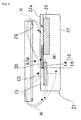
- Fig. 1 is a diagram illustrating a manner in which a mobile information terminal 21 disclosed in Patent Literature 1 and a reader/writer communicate with each other when they are in close proximity to each other.
- a part of a magnetic field H of an electromagnetic wave emitted from a transmission/receiving antenna portion 26 in the reader/writer is reflected or absorbed under the effect of a metal body such as a battery pack 25 in a terminal body 22 and is attenuated.
- a metal layer 30 is disposed so that it is nearer to an electromagnetic wave enter side than a communication surface CS of an antenna module 10.
- an induced current (eddy current) occurs on the surface of the metal layer 30 and a magnetic field H1 is generated.
- the magnetic field H1 generates an induced current at an antenna coil 15 in the antenna module 10.
- An antenna apparatus includes a power supply coil including a loop or spiral coil conductor having a coil window at a winding center, a booster electrode that faces the power supply coil and includes a conductor aperture and a slit portion connected to the conductor aperture, a conductor layer facing the power supply coil or the booster electrode, and a magnetic layer disposed between the power supply coil or the booster electrode and the conductor layer.
- the magnetic layer covers the conductor aperture and the slit portion of the booster electrode in plan view of the power supply coil, the booster electrode, the conductor layer, and the magnetic layer.
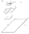
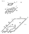
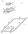
- Fig. 2 is an exploded perspective view of an antenna apparatus 101 according to the first embodiment.
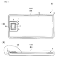
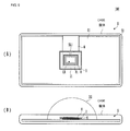
- Fig. 3(A) is a plan view of a communication terminal including the antenna apparatus 101.
- Fig. 3(B) is an elevational view of the communication terminal.
- the booster electrode sheet 7 includes an insulating substrate 70 and a booster electrode 71 formed on the insulating substrate 70.
- the booster electrode 71 is a C-shaped conductor film, and is disposed so that it faces the power supply coil 8.
- the booster electrode sheet 7 includes a conductor region covering the coil conductor 81 in plan view, a conductor aperture (nonconductor region) CA covering the coil window CW in plan view, and a slit portion SL1 connecting the outer edge of the conductor region and the conductor aperture CA.
- the power supply coil 8 and the booster electrode 71 are disposed so that the opening of the coil conductor 81 and the conductor aperture CA of the booster electrode 71 at least partly cover in plan view.
- the magnetic sheet 6 covers a region slightly larger than a region including the conductor aperture CA and the slit portion SL1 of the booster electrode 71. Accordingly, a magnetic flux generated by a current flowing around the conductor aperture CA of the booster electrode 71 and a current flowing along both sides of the slit portion SL1 of the booster electrode 71 is hardly linked to the ground electrode 51. That is, the magnetic sheet 6 hides the current flowing around the conductor aperture CA of the booster electrode 71 from the ground electrode 51. Induced currents generated by the current flowing around the conductor aperture CA of the booster electrode 71 and the current flowing along the slit portion SL1 of the booster electrode 71 therefore hardly flow through the ground electrode 51.
- induced currents generated by the current flowing around the conductor aperture CA of the booster electrode 71 and the current flowing along both sides of the slit portion SL1 of the booster electrode 71 flow through the ground electrode 51. Since these induced currents flow near the induced currents generated by the currents flowing along the periphery of the booster electrode 71 in the direction opposite to that of the induced currents, magnetic fields cancel each other. As a result, the currents EC56, EC57, and EC58 illustrated in Fig. 4 become very small, and the currents EC51, EC52, EC53, EC54, and EC55 flowing along the periphery of the ground electrode 51 also become very small. In this example, since the magnetic sheet 6 is disposed as illustrated in Fig. 4 , the above-described magnetic field cancellation does not occur and a large current flows along the outer edge of the ground electrode 51.
- the set of the power supply coil 8, the booster electrode sheet 7, and the magnetic sheet 6 is disposed at a position that is apart from the edge of the ground electrode 51 in a direction in which the center of the ground electrode 51 is present.
Landscapes
- Engineering & Computer Science (AREA)
- Computer Networks & Wireless Communication (AREA)
- Signal Processing (AREA)
- Computer Hardware Design (AREA)
- Microelectronics & Electronic Packaging (AREA)
- Physics & Mathematics (AREA)
- General Physics & Mathematics (AREA)
- Theoretical Computer Science (AREA)
- Details Of Aerials (AREA)
- Support Of Aerials (AREA)
Abstract
Description
- The present invention relates to an antenna apparatus that communicates with another apparatus with an electromagnetic signal and is used in an RFID system and a short-range wireless communication system, and a communication terminal including the antenna apparatus.
- In RFID systems and short-range wireless communication systems that have been increasingly used in recent years, in order to allow a mobile electronic apparatus such as a mobile telephone to communicate with another mobile electronic apparatus or a reader/writer, communication antennas are included in these mobile electronic apparatuses and the reader/writer.
Patent Literature 1 discloses an antenna included in a mobile electronic apparatus. -
Fig. 1 is a diagram illustrating a manner in which amobile information terminal 21 disclosed inPatent Literature 1 and a reader/writer communicate with each other when they are in close proximity to each other. In an example illustrating inFig. 1 , a part of a magnetic field H of an electromagnetic wave emitted from a transmission/receivingantenna portion 26 in the reader/writer is reflected or absorbed under the effect of a metal body such as abattery pack 25 in aterminal body 22 and is attenuated. Ametal layer 30 is disposed so that it is nearer to an electromagnetic wave enter side than a communication surface CS of anantenna module 10. When a magnetic field is externally applied to the surface of themetal layer 30, an induced current (eddy current) occurs on the surface of themetal layer 30 and a magnetic field H1 is generated. The magnetic field H1 generates an induced current at anantenna coil 15 in theantenna module 10. - In this example, by disposing the
metal layer 30 so that it covers a part of theantenna coil 15 and faces theantenna module 10 in close proximity to theantenna module 10, the transmission/receivingantenna portion 26 in the reader/writer and theantenna coil 15 in theantenna module 10 are inductively coupled via the magnetic field component H1 generated at themetal layer 30. -
- PTL 1: Japanese Unexamined Patent Application Publication No.
2006-270681 - The antenna apparatus illustrated in
Fig. 1 solves a problem that a communication characteristic is markedly changed by a misalignment between the center of an antenna included therein and the center of an antenna included in a communication partner when these antennas are very close to each other. In order to prevent a magnetic flux to be linked to theantenna coil 15 in theantenna module 10 in themobile information terminal 21 and the transmission/receivingantenna portion 26 in the reader/writer from being interrupted by a metal body such as thebattery pack 25, themetal layer 30 is disposed to induce the magnetic flux. Accordingly, depending on the position of an interrupter such as thebattery pack 25, a significant effect may not be obtained.
Furthermore, themetal layer 30 may not be effective in increasing a communication range when an antenna in an antenna apparatus and an antenna in a communication partner are apart from each other. - It is an object of the present invention to provide an antenna apparatus capable of stably communicating with a communication partner and increasing the maximum possible communication range even when an antenna included therein is relatively smaller than an antenna included in the communication partner.
- An antenna apparatus according to the present invention includes a power supply coil including a loop or spiral coil conductor having a coil window at a winding center, a booster electrode that faces the power supply coil and includes a conductor aperture and a slit portion connected to the conductor aperture, a conductor layer facing the power supply coil or the booster electrode, and a magnetic layer disposed between the power supply coil or the booster electrode and the conductor layer. The magnetic layer covers the conductor aperture and the slit portion of the booster electrode in plan view of the power supply coil, the booster electrode, the conductor layer, and the magnetic layer.
- A communication terminal according to the present invention includes an antenna apparatus. The antenna apparatus includes a power supply coil including a loop or spiral coil conductor having a coil window at a winding center, a booster electrode that faces the power supply coil and includes a conductor aperture and a slit portion connected to the conductor aperture, a conductor layer facing the power supply coil or the booster electrode, and a magnetic layer disposed between the power supply coil or the booster electrode and the conductor layer. The magnetic layer covers the conductor aperture and the slit portion of the booster electrode in plan view of the power supply coil, the booster electrode, the conductor layer, and the magnetic layer.
- According to the present invention, a current flows through a booster electrode while interrupting a magnetic field generated by a current flowing through a coil conductor. A current flowing around a conductor aperture of the booster electrode flows to the outer edge of the booster electrode via a periphery of a slit portion. An induced current having the same direction as that of the current flowing around the booster electrode is generated at a conductor layer. As a result, the strength of magnetic fields generated from a power supply coil, the booster electrode, and the conductor layer is increased, and a communication range can be increased.
-
- [
Fig. 1] Fig. 1 is a diagram illustrating a manner in which amobile information terminal 21 and a reader/writer communicate with each other when they are in close proximity to each other inPatent Literature 1. - [
Fig. 2] Fig. 2 is an exploded perspective view of anantenna apparatus 101 according to a first embodiment. - [
Fig. 3] Fig. 3(A) is a plan view of a communication terminal including theantenna apparatus 101, andFig. 3(B) is an elevational view of the communication terminal. - [
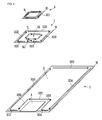
Fig. 4] Fig. 4 is a diagram illustrating a current passing through acoil conductor 81 of apower supply coil 8, a current passing through abooster electrode 71 of abooster electrode sheet 7, and a current passing through aground electrode 51 of aground substrate 5. - [
Fig. 5] Figs. 5(A) and 5(B) are diagrams illustrating the relationship between the positional relationship between theground substrate 5 and amagnetic sheet 6 and a current passing through theground electrode 51. - [
Fig. 6] Fig. 6 is a diagram illustrating currents flowing in a state in which thepower supply coil 8, thebooster electrode sheet 7, themagnetic sheet 6, and theground substrate 5 are laminated. - [
Fig. 7] Fig. 7 is an exploded perspective view of anantenna apparatus 102 according to a second embodiment. - [
Fig. 8] Fig. 8 is an exploded perspective view of anantenna apparatus 103 according to a third embodiment. - [
Fig. 9] Fig. 9(A) is a plan view of anantenna apparatus 104 according to a fourth embodiment, andFig. 9(B) is an elevational view of theantenna apparatus 104. - [
Fig. 10] Fig. 10 is an exploded perspective view of anantenna apparatus 105 according to a fifth embodiment. - [
Fig. 11] Fig. 11 is an exploded perspective view illustrating currents flowing through thecoil conductor 81 of thepower supply coil 8, thebooster electrode 71 of thebooster electrode sheet 7, and theground electrode 51 of theground substrate 5 in a comparative example of an antenna apparatus according to a sixth embodiment. - [
Fig. 12] Fig. 12 is an exploded perspective view illustrating currents flowing through thecoil conductor 81 of thepower supply coil 8, thebooster electrode 71 of thebooster electrode sheet 7, and theground electrode 51 of theground substrate 5 in anantenna apparatus 106 according to the sixth embodiment. - [
Fig. 13] Fig. 13 is a plan view of theantenna apparatus 106 according to the sixth embodiment. - An antenna apparatus according to the first embodiment and a communication terminal including the antenna apparatus will be described with reference to
Figs. 2 to 6 .
Fig. 2 is an exploded perspective view of anantenna apparatus 101 according to the first embodiment.Fig. 3(A) is a plan view of a communication terminal including theantenna apparatus 101.Fig. 3(B) is an elevational view of the communication terminal. - An antenna module according to this embodiment is used in NFC (Near Field Communication: short-range communication) such as Felica (registered trademark) and uses the HF band having a center frequency of 13.56 MHz.
- The
antenna apparatus 101 illustrated inFig. 2 includes apower supply coil 8, abooster electrode sheet 7, amagnetic sheet 6, and aground substrate 5 in this order from the top. Theantenna apparatus 101 is a laminate of these parts. - The
power supply coil 8 is obtained by forming aspiral coil conductor 81 on aflexible substrate 80 that is a rectangular plate-like insulating substrate. Thespiral coil conductor 81 has a coil window CW at a winding center, and can therefore emit a magnetic field appropriately. A connection portion (not illustrated) used for connection between the coil conductor and an external circuit is formed at theflexible substrate 80. - The number of windings (turns) of the
coil conductor 81 is determined in accordance with a required inductance, and may be one. In this case, thecoil conductor 81 is a loop coil conductor. Thecoil conductor 81 may be formed in a single plane or a plurality of layers. - The
booster electrode sheet 7 includes aninsulating substrate 70 and abooster electrode 71 formed on theinsulating substrate 70. Thebooster electrode 71 is a C-shaped conductor film, and is disposed so that it faces thepower supply coil 8. Thebooster electrode sheet 7 includes a conductor region covering thecoil conductor 81 in plan view, a conductor aperture (nonconductor region) CA covering the coil window CW in plan view, and a slit portion SL1 connecting the outer edge of the conductor region and the conductor aperture CA. - The
magnetic sheet 6 is, for example, a ferrite sheet. As will be described later, themagnetic sheet 6 covers thebooster electrode sheet 7 so that it covers a region slightly larger than a region including the conductor aperture CA and the slit portion SL1 of thebooster electrode 71. - The
ground substrate 5 includes aninsulating substrate 50 and aground electrode 51 formed on the upper surface of theinsulating substrate 50. Theground electrode 51 corresponds to a conductor layer according to the present invention. A printed circuit board disposed in a case of a communication terminal can be used as theground substrate 5, and a ground electrode disposed at the printed circuit board can be used as theground electrode 51. - As illustrated in
Figs. 3(A) and 3(B) , a laminate including thepower supply coil 8, thebooster electrode sheet 7, and themagnetic sheet 6 is disposed near the center of one short side of theground substrate 5.
Thepower supply coil 8 is disposed so that thecoil conductor 81 surrounds the conductor aperture CA of thebooster electrode 71. When thecoil conductor 81 surrounds the conductor aperture CA of thebooster electrode 71 as described above, a region in which thecoil conductor 81 and thebooster electrode 71 cove in plan view is increased. As a result, the degree of coupling between thepower supply coil 8 and thebooster electrode 71 is increased. It is desired that the shape of thebooster electrode 81 be designed on the basis of the shape of thecoil conductor 81. - The
power supply coil 8 and thebooster electrode 71 are disposed so that the opening of thecoil conductor 81 and the conductor aperture CA of thebooster electrode 71 at least partly cover in plan view. - The
magnetic sheet 6 is disposed so that it covers a region slightly larger than a region including the conductor aperture CA and the slit portion SL1 of thebooster electrode 71. That is, thebooster electrode 71 includes a region covering the magnetic sheet 6 (a region around the conductor aperture CA and the slit portion SL1) and a region that does not cover the magnetic sheet 6 (the outer edge). -
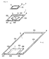
Fig. 4 is a diagram illustrating a current passing through thecoil conductor 81 of thepower supply coil 8, a current passing through thebooster electrode 71 of thebooster electrode sheet 7, and a current passing through theground electrode 51 of theground substrate 5. These currents are obtained under conditions where thepower supply coil 8, thebooster electrode sheet 7, themagnetic sheet 6, and theground substrate 5 are laminated. - As illustrated in
Fig. 4 , when a current EC3 flows through thecoil conductor 81 of thepower supply coil 8, a magnetic flux generated from thecoil conductor 81 attempts to link to thebooster electrode 71. Accordingly, a current (induced current) that interrupts the magnetic flux flows around the conductor aperture CA of thebooster electrode 71 in a direction opposite to that of the current passing through thecoil conductor 81. The current around the conductor aperture CA flows along the slit portion SL1, and then flows along the periphery of thebooster electrode 71, that is, the outer edge of thebooster electrode 71. Since the current flows along the periphery of thebooster electrode 71, a magnetic field emission area is increased. Thebooster electrode 71 functions as a booster for increasing the size of a magnetic flux loop. Thus, thecoil conductor 81 of thepower supply coil 8 and thebooster electrode 71 are coupled mainly via a magnetic field. - On the other hand, the
magnetic sheet 6 covers a region slightly larger than a region including the conductor aperture CA and the slit portion SL1 of thebooster electrode 71. Accordingly, a magnetic flux generated by a current flowing around the conductor aperture CA of thebooster electrode 71 and a current flowing along both sides of the slit portion SL1 of thebooster electrode 71 is hardly linked to theground electrode 51. That is, themagnetic sheet 6 hides the current flowing around the conductor aperture CA of thebooster electrode 71 from theground electrode 51. Induced currents generated by the current flowing around the conductor aperture CA of thebooster electrode 71 and the current flowing along the slit portion SL1 of thebooster electrode 71 therefore hardly flow through theground electrode 51. - Induced currents EC58, EC57, and EC56 generated by currents EC22, EC23, and EC24, respectively, flowing along the outer edge of the
booster electrode 71 flow through theground electrode 51 of theground substrate 5. As a result, following the currents EC56, EC57, and EC58, currents EC51, EC52, EC53, EC54, and EC55 flow along the periphery of theground electrode 51. That is, a current loop is formed in a path of the currents EC51 → EC52 → EC53 → EC54 → EC55 → EC56 → EC57 → EC58. The current loop increases the magnetic field emission area and can increase the size of a magnetic flux loop. - Thus, the
booster electrode 71 and theground electrode 51 are coupled mainly via a magnetic field. - If the
magnetic sheet 6 is not present, induced currents generated by the current flowing around the conductor aperture CA of thebooster electrode 71 and the current flowing along both sides of the slit portion SL1 of thebooster electrode 71 flow through theground electrode 51. Since these induced currents flow near the induced currents generated by the currents flowing along the periphery of thebooster electrode 71 in the direction opposite to that of the induced currents, magnetic fields cancel each other. As a result, the currents EC56, EC57, and EC58 illustrated inFig. 4 become very small, and the currents EC51, EC52, EC53, EC54, and EC55 flowing along the periphery of theground electrode 51 also become very small.
In this example, since themagnetic sheet 6 is disposed as illustrated inFig. 4 , the above-described magnetic field cancellation does not occur and a large current flows along the outer edge of theground electrode 51. - Since the
magnetic sheet 6 protrudes from thebooster electrode 71 in an extension direction from the conductor aperture to the slit portion of thebooster electrode 71 in plan view, the coupling between the current flowing along both sides of the slit portion SL1 of thebooster electrode 71 and theground electrode 51 is prevented with certainty. As a result, the induced current generated by the current flowing along both sides of the slit portion SL1 can be prevented from flowing through theground electrode 51 with certainty. As described previously, the induced current that is generated by the current flowing along the slit portion SL1 and attempts to flow through theground electrode 51 is a current flowing in a direction opposite to that of the currents EC56, EC57, and EC58. Accordingly, themagnetic sheet 6 can prevent the induced current generated by the current flowing along the slit portion SL1 of thebooster electrode 71 from flowing through theground electrode 51 with more certainty. That is, the occurrence of a current flowing along the outer edge of theground electrode 51 can be prevented and a large current can flow along the periphery of thebooster electrode 71. -
Fig. 5(A) illustrates the positional relationship between theground substrate 5 and themagnetic sheet 6 in an antenna apparatus according to the first embodiment.Fig. 5(B) illustrates a comparative example. As illustrated inFig. 5(B) , when themagnetic sheet 6 is inside the outer edge of theground electrode 51 in plan view, the current flowing along the periphery of themagnetic sheet 6 has a loop of the currents EC56 → EC57 → EC58 → a current EC59. That is, a shortcut current flows. On the other hand, as illustrated inFig. 5(A) , when themagnetic sheet 6 protrudes from the outer edge of theground electrode 51 in the extension direction from the conductor aperture to the slit of thebooster electrode 71 by a protrusion distance T in plan view, the occurrence of the above-described shortcut current is prevented and the currents EC51, EC52, EC53, EC54, and EC55 flowing along the periphery of theground electrode 51 become large. The reason for this is that an inductance component is increased in a region where the magnetic sheet is close to theground electrode 51. That is, the large currents EC51, EC52, EC53, EC54, and EC55 flow in a path along the periphery of the ground electrode while avoiding the region. Themagnetic sheet 6 may reach just the outer edge of theground electrode 51 in the extension direction from the conductor aperture to the slit of thebooster electrode 71. The protrusion distance T is determined in consideration of the accuracy of attachment of themagnetic sheet 6 to theground electrode 51. -
Fig. 6 is a diagram illustrating currents flowing in a state in which thepower supply coil 8, thebooster electrode sheet 7, themagnetic sheet 6, and theground substrate 5 are laminated.
As illustrated inFig. 6 , the directions of a current flowing through thecoil conductor 81, a current flowing through a main part (other than both sides of the slit portion SL1) of thebooster electrode 71, and a current flowing through theground electrode 51 are the same, and magnetic fields generated by these currents are added (these currents do not cancel one another). Accordingly, as compared with a case where thepower supply coil 8 is singly used and a case where the combination of thepower supply coil 8 and thebooster electrode sheet 7 is used, a higher antenna gain can be obtained. - Referring to
Fig. 3(B) , a curve DG represents an emitted magnetic field strength pattern that is the directional characteristic of theantenna apparatus 101. As illustrated in the drawing, directivity is high in a direction in which the slit portion SL1 of thebooster electrode 71 is present, and the center of the directivity is shifted in an oblique direction with respect to the position of the laminate including thepower supply coil 8, thebooster electrode sheet 7, and themagnetic sheet 6 as viewed from the center of theground electrode 51. The reason for this is that the intensity distribution of a current flowing through theground electrode 51 is concentrated at a position nearer to the laminate than to the center of theground electrode 51 because not only a magnetic field generated from theground electrode 51 but also magnetic fields generated from thecoil conductor 81 and thebooster electrode 71 contribute to emission. Accordingly, when the slit portion SL1 of thebooster electrode 71 is disposed so that it is directed toward the tip of a case of a mobile telephone terminal, such mobile telephone terminals are suitable for use in communication between them diagonally close to each other. - In the first embodiment, the
magnetic sheet 6 covers a region slightly larger than the region including the conductor aperture CA and the slit portion SL1 of thebooster electrode 71 in plan view, but may just cover the conductor aperture CA and the slit portion SL1 of thebooster electrode 71. - A current flowing along the outer edge of the
booster electrode 71 and a current flowing around the conductor aperture CA are opposite in direction. Therefore, in the intensity distribution of a current flowing through thebooster electrode 71, a line indicating the current value of zero is generated at a midpoint between the outer edge and the inner edge (the outer edge of the conductor aperture CA) of thebooster electrode 71. Ideally, the size and position of themagnetic sheet 6 are determined so that the outer edge of themagnetic sheet 6 matches the line indicating the current value of zero. - Thus, since the
booster electrode 71 has a region (coupling region) that does not cover themagnetic sheet 6 in plan view, thebooster electrode 71 functions as a booster. - In the present invention, the ground electrode (conductor layer) 51, the
booster electrode 71, and thecoil conductor 81 function as radiating elements. However, among them, the conductor layer is a main radiating element. -
Fig. 7 is an exploded perspective view of anantenna apparatus 102 according to the second embodiment.
Theantenna apparatus 102 illustrated inFig. 7 includes thepower supply coil 8, thebooster electrode sheet 7, themagnetic sheet 6, and theground substrate 5 in this order from the top. Theantenna apparatus 102 is the laminate of these parts. - The shape of the
magnetic sheet 6 is different from the shape of themagnetic sheet 6 in theantenna apparatus 101 according to the first embodiment illustrated inFig. 2 . Referring toFig. 7 , a chain double-dashed line represents a position at which themagnetic sheet 6 covers thebooster electrode sheet 7. Themagnetic sheet 6 not only covers the conductor aperture CA and the slit portion SL1 of thebooster electrode 71, but also extends to a region where the slit portion SL1 divides the periphery, that is, a region where the currents EC21 and EC25 flow. - In the case of the above-described structure, induced currents generated by the currents EC21 and EC25, respectively, hardly flow through the
ground electrode 51. The induced currents that are generated by the currents EC21 and EC25, respectively, and attempt to flow through theground electrode 51 is opposite in direction to the currents EC51, EC52, EC53, EC54, and EC55. Accordingly, when themagnetic sheet 6 prevents the induced currents generated by the currents EC21 and EC25, respectively, flowing through thebooster electrode 71 from flowing through theground electrode 51, an antenna gain is further increased. -
Fig. 8 is an exploded perspective view of anantenna apparatus 103 according to the third embodiment.
Theantenna apparatus 103 illustrated inFig. 8 includes thebooster electrode sheet 7, thepower supply coil 8, themagnetic sheet 6, and theground substrate 5 in this order from the top. Theantenna apparatus 103 is the laminate of these parts. - The positional relationship between the
booster electrode sheet 7 and thepower supply coil 8 is different from that in theantenna apparatus 101 according to the first embodiment illustrated inFig. 2 . Thus, thepower supply coil 8 may be present between thebooster electrode sheet 7 and themagnetic sheet 6. That is, a current flowing around the conductor aperture CA of thebooster electrode 71 and a current flowing along both sides of the slit portion SL1 of thebooster electrode 71 are interrupted by themagnetic sheet 6, and only a current flowing along the outer edge of thebooster electrode 71 is practically guided to theground electrode 51. - Since the
magnetic sheet 6 is larger than thepower supply coil 8, a current flowing through thecoil conductor 81 of thepower supply coil 8 becomes invisible from theground electrode 51. That is, themagnetic sheet 6 hides the current flowing through thecoil conductor 81. Accordingly, it is possible to prevent a reactive induced current (an induced current in the opposite direction) from flowing through theground electrode 51. -
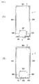
Fig. 9(A) is a plan view of anantenna apparatus 104 according to the fourth embodiment, andFig. 9(B) is an elevational view of theantenna apparatus 104. In this example, the laminate including thepower supply coil 8, thebooster electrode sheet 7, and themagnetic sheet 6 is disposed at substantially the center of theground substrate 5. Themagnetic sheet 6 is disposed in the extension direction from the conductor aperture to the slit portion SL1 of thebooster electrode 71 formed on thebooster electrode sheet 7. The leading end of themagnetic sheet 6 reaches the center of one long side of theground substrate 5.
Dislike in the example according to the first embodiment illustrated inFigs. 3(A) and 3(B) , the laminate including thepower supply coil 8, thebooster electrode sheet 7, and themagnetic sheet 6 is disposed at substantially the center of theground substrate 5, and themagnetic sheet 6 extends for a relatively long distance to the edge of theground electrode 51. In order to prevent themagnetic sheet 6 from being too long, the slit portion SL1 of thebooster electrode 71 is directed toward the long side of theground substrate 5. - Referring to
Fig. 9(B) , the curve DG represents an emitted magnetic field strength pattern that is the directional characteristic of theantenna apparatus 104. As illustrated in the drawing, since thepower supply coil 8, thebooster electrode sheet 7, themagnetic sheet 6, and theground electrode 51 are substantially rotationally symmetric with respect to the center of theground electrode 51, the center of the directivity is directed in the direction of the normal to theground electrode 51. Such directivity characteristic is suitable for use in communication between an antenna in a reader/writer and an antenna apparatus facing the antenna. -
Fig. 10 is an exploded perspective view of anantenna apparatus 105 according to the fifth embodiment.
Theantenna apparatus 105 illustrated inFig. 10 includes thepower supply coil 8, thebooster electrode sheet 7, themagnetic sheet 6, and theground substrate 5 in this order from the top. Theantenna apparatus 105 is the laminate of these parts. - The shape of the
magnetic sheet 6 is different from the shape of themagnetic sheet 6 in theantenna apparatus 101 according to the first embodiment illustrated inFig. 2 . Referring toFig. 10 , a chain double-dashed line represents a position at which themagnetic sheet 6 covers thebooster electrode sheet 7. Themagnetic sheet 6 covers the conductor aperture CA and the slit portion SL1 of thebooster electrode 71, and the width of a portion of themagnetic sheet 6 covering the slit portion SL1 is small. - Dislike in the first embodiment, the set of the
power supply coil 8, thebooster electrode sheet 7, and themagnetic sheet 6 is disposed at a position that is apart from the edge of theground electrode 51 in a direction in which the center of theground electrode 51 is present. - In the case of the above-described structure, induced currents EC61 and EC57 generated by the currents EC21 and EC25, respectively, flow through the
ground electrode 51. Since the width of the portion of themagnetic sheet 6 covering the slit portion SL1 is small, the currents EC56 and EC62 flow along both sides of the thin portion of themagnetic sheet 6. A current loop is formed in a path of the currents EC51 → EC52 → EC53 → EC54 → EC55 → EC56 → EC57 → EC58 → EC59 → EC60 → EC61 → EC62. The current loop increases the magnetic field emission area and can increase the size of a magnetic flux loop. - An antenna apparatus according to the sixth embodiment will be described with reference to
Figs. 11 to 13 .Fig. 11 is an exploded perspective view illustrating currents flowing through thecoil conductor 81 of thepower supply coil 8, thebooster electrode 71 of thebooster electrode sheet 7, and theground electrode 51 of theground substrate 5 in a comparative example of an antenna apparatus according to the sixth embodiment. - A structure similar to the structure according to the first embodiment illustrated in
Fig. 4 is provided. When the current interruption effect of themagnetic sheet 6 is weak, a shortcut current EC58 represented by a broken line inFig. 11 may flow. In this case, since a magnetic field generated by a current flowing through thebooster electrode 71 is partly eliminated, the characteristic is deteriorated. -
Fig. 12 is an exploded perspective view illustrating currents flowing through thecoil conductor 81 of thepower supply coil 8, thebooster electrode 71 of thebooster electrode sheet 7, and theground electrode 51 of theground substrate 5 in anantenna apparatus 106 according to the sixth embodiment. A slit portion SL2 is disposed at theground electrode 51 so that it interrupts the current EC58 illustrated inFig. 11 . With this structure, the occurrence of the shortcut current EC58 can be prevented with certainty. -
Fig. 13 is a plan view of theantenna apparatus 106. As illustrated inFig. 13 , the slit portion SL2 of theground electrode 51 is preferably formed so that it extends in a direction in which the slit portion SL1 of thebooster electrode 71 extends and covers the slit portion SL1. A length L of the slit portion SL2 is preferably set so that the leading end of the slit portion SL2 is inside the conductor aperture CA. Referring toFig. 13 , a dimension min represents an example of the minimum dimension of the slit portion SL2, and a dimension max represents an example of the maximum dimension of the slit portion SL2. - When the slit portion SL2 is formed at the
ground electrode 51, a necessary induced current can be generated and the occurrence of a shortcut current can be prevented with more certainty. - The directional characteristic of an antenna apparatus can be changed by changing the shape of a magnetic sheet. Alternatively, the directional characteristic of an antenna apparatus can be changed by adjusting the position, width, and length of the slit portion SL1. Since a large potential difference is obtained at the slit portion SL1 and a strong magnetic field is emitted, the directional characteristic can be changed by changing the position of the slit portion. For example, the directional characteristic is improved by reducing the width of the slit portion SL1 or increasing the length of the slit portion SL1.
- The conductor aperture CA and the slit portion SL1 of the booster electrode may have the same width.
- The magnetic sheet may not necessarily be a single sintered ferrite plate, and may be obtained by attaching a double-faced adhesive sheet for flexible substrate attachment and a single-faced adhesive sheet for protection to both surfaces of a sintered magnetic substance and dividing the sintered magnetic substance into small pieces. The sintered magnetic substance may not necessarily be used, and a composite composed of ferrite and a resin or a metal magnetic substance may be used.
- An antenna apparatus using an HF band having a center frequency of 13.56 MHz has been described in the above-described embodiments. However, the present invention can be employed in a frequency band other than the HF band. For example, an antenna apparatus according to the present invention can be used as an antenna for an RFID tag using the 900 MHz UHF band. In this case, the coil conductor of the power supply coil and the booster electrode are coupled mainly via an electromagnetic field, and the booster electrode and the ground electrode are coupled mainly via an electromagnetic field.
- The positional relationship between the power supply coil and the booster electrode may be changed. Reference Signs List
-
- CA
- conductor aperture
- CW
- coil window
- SL1, SL2
- slit portion
- 5
- ground substrate
- 50
- insulating substrate
- 51
- ground electrode (conductor layer)
- 6
- magnetic sheet (magnetic layer)
- 7
- booster electrode sheet
- 70
- insulating substrate
- 71
- booster electrode
- 8
- power supply coil
- 80
- flexible substrate
- 81
- coil conductor
- 101 to 106
- antenna apparatus
Claims (8)
- An antenna apparatus comprising:a power supply coil including a loop or spiral coil conductor having a coil window at a winding center;a booster electrode that faces the power supply coil and includes a conductor aperture and a slit portion connected to the conductor aperture;a conductor layer facing the power supply coil or the booster electrode; anda magnetic layer disposed between the power supply coil or the booster electrode and the conductor layer, andwherein the magnetic layer covers the conductor aperture and the slit portion of the booster electrode in plan view of the power supply coil, the booster electrode, the conductor layer, and the magnetic layer.
- The antenna apparatus according to Claim 1, wherein the booster electrode includes a region that does not cover the magnetic layer in plan view of the power supply coil, the booster electrode, the conductor layer, and the magnetic layer.
- The antenna apparatus according to Claim 1 or 2, wherein the magnetic layer protrudes from the booster electrode in an extension direction from the conductor aperture to the slit portion of the booster electrode in plan view of the power supply coil, the booster electrode, the conductor layer, and the magnetic layer.
- The antenna apparatus according to any one of Claims 1 to 3, wherein the magnetic layer reaches an outer edge of the conductor layer or a position apart from the outer edge of the conductor layer in the extension direction from the conductor aperture to the slit portion of the booster electrode in plan view of the power supply coil, the booster electrode, the conductor layer, and the magnetic layer.
- The antenna apparatus according to any one of Claims 1 to 4, wherein the power supply coil, the booster electrode, the magnetic layer, and the conductor layer are disposed in this order so that they face one another.
- The antenna apparatus according to any one of Claims 1 to 5, wherein the power supply coil and the booster electrode are coupled to each other via an electromagnetic field or a magnetic field, and the booster electrode and the conductor layer are coupled to each other via an electromagnetic field or a magnetic field.
- The antenna apparatus according to any one of Claims 1 to 6, wherein the power supply coil and the conductor layer are coupled to each other via an electromagnetic field or a magnetic field.
- A communication terminal comprising an antenna apparatus including:a power supply coil including a loop or spiral coil conductor having a coil window at a winding center;a booster electrode that faces the power supply coil and includes a conductor aperture and a slit portion connected to the conductor aperture;a conductor layer facing the power supply coil or the booster electrode; anda magnetic layer disposed between the power supply coil or the booster electrode and the conductor layer, andwherein the magnetic layer covers the conductor aperture and the slit portion of the booster electrode in plan view of the power supply coil, the booster electrode, the conductor layer, and the magnetic layer.
Applications Claiming Priority (2)
| Application Number | Priority Date | Filing Date | Title |
|---|---|---|---|
| JP2010091086 | 2010-04-12 | ||
| PCT/JP2011/054088 WO2011129151A1 (en) | 2010-04-12 | 2011-02-24 | Antenna device and communication terminal device |
Publications (2)
| Publication Number | Publication Date |
|---|---|
| EP2515377A1 true EP2515377A1 (en) | 2012-10-24 |
| EP2515377A4 EP2515377A4 (en) | 2014-12-24 |
Family
ID=44798530
Family Applications (1)
| Application Number | Title | Priority Date | Filing Date |
|---|---|---|---|
| EP11768672.5A Withdrawn EP2515377A4 (en) | 2010-04-12 | 2011-02-24 | Antenna device and communication terminal device |
Country Status (6)
| Country | Link |
|---|---|
| US (2) | US9595749B2 (en) |
| EP (1) | EP2515377A4 (en) |
| JP (1) | JP4934784B2 (en) |
| KR (1) | KR101306897B1 (en) |
| CN (1) | CN102714355B (en) |
| WO (1) | WO2011129151A1 (en) |
Families Citing this family (55)
| Publication number | Priority date | Publication date | Assignee | Title |
|---|---|---|---|---|
| GB2495418B (en) * | 2010-07-28 | 2017-05-24 | Murata Manufacturing Co | Antenna apparatus and communication terminal instrument |
| WO2013011865A1 (en) * | 2011-07-19 | 2013-01-24 | 株式会社村田製作所 | Antenna module, antenna device, rfid tag, and communication terminal device |
| JP5609922B2 (en) * | 2011-08-10 | 2014-10-22 | 株式会社村田製作所 | Antenna device and communication terminal device |
| CN103620868B (en) * | 2012-02-01 | 2016-06-08 | 株式会社村田制作所 | Antenna device and communication terminal device |
| WO2013156389A1 (en) * | 2012-04-19 | 2013-10-24 | Smartrac Ip B.V. | Integrated loop structure for radio frequency identification |
| JP5772868B2 (en) * | 2012-05-21 | 2015-09-02 | 株式会社村田製作所 | ANTENNA DEVICE AND WIRELESS COMMUNICATION DEVICE |
| US9083073B2 (en) * | 2012-06-28 | 2015-07-14 | Intel Corporation | Thin chassis near field communication (NFC) antenna integration |
| GB2519247B (en) * | 2012-06-28 | 2017-11-29 | Murata Manufacturing Co | Antenna device, feed element, and communication terminal device |
| JP5964155B2 (en) * | 2012-06-28 | 2016-08-03 | Necトーキン株式会社 | Antenna device |
| JP6131418B2 (en) * | 2012-11-26 | 2017-05-24 | スミダコーポレーション株式会社 | Electronics |
| JP2014135448A (en) * | 2013-01-11 | 2014-07-24 | Taiyo Yuden Co Ltd | Electronic component |
| WO2014167812A1 (en) * | 2013-04-12 | 2014-10-16 | パナソニック株式会社 | Antenna, antenna device and communication device |
| KR102158858B1 (en) * | 2013-07-03 | 2020-09-22 | 삼성전자주식회사 | Cover of a portable device, and portable device |
| US20150009077A1 (en) * | 2013-07-03 | 2015-01-08 | Samsung Electronics Co., Ltd. | Cover of a mobile device and mobile device including the same |
| CN206098727U (en) * | 2013-07-16 | 2017-04-12 | 株式会社村田制作所 | Antenna device and communication device electronic equipment |
| WO2015016353A1 (en) * | 2013-08-02 | 2015-02-05 | 株式会社村田製作所 | Antenna device and communication terminal |
| JP6187097B2 (en) * | 2013-09-27 | 2017-08-30 | Tdk株式会社 | Antenna device |
| CN204810312U (en) | 2013-12-26 | 2015-11-25 | 株式会社村田制作所 | communication terminal device |
| US10461582B2 (en) * | 2014-03-31 | 2019-10-29 | Qualcomm Incorporated | Systems, apparatus, and methods for wireless power receiver coil configuration |
| JP6318826B2 (en) * | 2014-04-30 | 2018-05-09 | Tdk株式会社 | Antenna device |
| US10290934B2 (en) | 2014-04-30 | 2019-05-14 | Tdk Corporation | Antenna device |
| US10014578B2 (en) | 2014-05-05 | 2018-07-03 | Nxp B.V. | Body antenna system |
| US10015604B2 (en) | 2014-05-05 | 2018-07-03 | Nxp B.V. | Electromagnetic induction field communication |
| US10009069B2 (en) | 2014-05-05 | 2018-06-26 | Nxp B.V. | Wireless power delivery and data link |
| CN207250728U (en) * | 2014-05-30 | 2018-04-17 | 株式会社村田制作所 | Antenna assembly and electronic equipment |
| US9608327B1 (en) * | 2014-06-24 | 2017-03-28 | Amazon Technologies, Inc. | Magnetically boosted NFC antenna |
| CN105745788B (en) * | 2014-09-12 | 2019-02-26 | 阿莫技术有限公司 | Multi-loop antenna module and portable terminal having the same |
| KR101622173B1 (en) * | 2014-10-14 | 2016-05-18 | 주식회사 이엠따블유 | Antenna |
| KR20160063191A (en) | 2014-11-26 | 2016-06-03 | 삼성전기주식회사 | Antenna device and Near field communication device including the same |
| US10014588B2 (en) * | 2014-12-05 | 2018-07-03 | Samsung Electro-Mechanics Co., Ltd. | Near-field antenna apparatus using eddy current and electronic device including the same |
| DE102015102288B4 (en) * | 2015-02-18 | 2019-02-07 | Infineon Technologies Ag | Chip card reader assembly |
| JP2016178527A (en) * | 2015-03-20 | 2016-10-06 | Tdk株式会社 | Antenna device |
| US10554078B2 (en) | 2015-04-24 | 2020-02-04 | Intel Corporation | Method and apparatus for coil integration for uniform wireless charging |
| CN105161819A (en) * | 2015-06-23 | 2015-12-16 | 瑞声精密制造科技(常州)有限公司 | Rfid antenna structure |
| US20170005395A1 (en) * | 2015-06-30 | 2017-01-05 | Tdk Corporation | Antenna device |
| CN104934692B (en) * | 2015-07-02 | 2017-03-22 | 上海安费诺永亿通讯电子有限公司 | NFC/RFID antenna apparatus and mobile terminal thereof |
| CN105024162B (en) * | 2015-07-08 | 2018-06-26 | 深圳市信维通信股份有限公司 | A kind of NFC antenna with metal rear shell |
| CN106410369B (en) * | 2015-07-31 | 2019-11-05 | 比亚迪股份有限公司 | The shell of NFC antenna mould group, mobile terminal and mobile terminal |
| KR102507947B1 (en) | 2015-10-15 | 2023-03-09 | 삼성전자주식회사 | Case and Electronic device including the same |
| US10090592B2 (en) * | 2015-10-29 | 2018-10-02 | Sonitus Technologies Inc. | Communication device |
| US9787368B2 (en) * | 2015-11-06 | 2017-10-10 | Mediatek Inc. | Antenna having passive booster for near field communication |
| US10320086B2 (en) * | 2016-05-04 | 2019-06-11 | Nxp B.V. | Near-field electromagnetic induction (NFEMI) antenna |
| WO2018028486A1 (en) | 2016-08-08 | 2018-02-15 | Guangdong Oppo Mobile Telecommunications Corp., Ltd. | Housing, method for manufacturing housing, and mobile terminal having housing |
| US10074891B2 (en) | 2016-09-02 | 2018-09-11 | AQ Corporation | Smartphone antenna in flexible PCB |
| US10547112B2 (en) | 2016-09-02 | 2020-01-28 | AQ Corporation | Smartphone antenna in flexible PCB |
| US10003120B2 (en) | 2016-09-02 | 2018-06-19 | AQ Corporation | Smartphone antenna in flexible PCB |
| USD850424S1 (en) | 2016-12-14 | 2019-06-04 | AQ Corporation | Flexible PCB dual antenna module for use in smartphone |
| WO2018113341A1 (en) * | 2016-12-23 | 2018-06-28 | Guangdong Oppo Mobile Telecommunications Corp., Ltd. | Housing assembly for terminal, terminal and mobile phone |
| KR102121795B1 (en) * | 2018-05-04 | 2020-06-11 | 주식회사 아모텍 | Antenna module |
| CN112566440A (en) * | 2019-09-25 | 2021-03-26 | 中兴通讯股份有限公司 | Electronic component and terminal equipment |
| US11303011B2 (en) | 2019-11-27 | 2022-04-12 | AQ Corporation | Smartphone antenna in flexible PCB |
| KR102332612B1 (en) * | 2020-09-11 | 2021-12-01 | 주식회사 이엠따블유 | An antenna module and wireless communication device having the same |
| KR102484949B1 (en) * | 2021-06-22 | 2023-01-10 | 주식회사 썬웨이커뮤니케이션코리아 | Combo type ultra wide band/near frequency communication antenna module |
| CN113869479B (en) * | 2021-09-28 | 2025-03-21 | 上扬无线射频科技扬州有限公司 | A multi-purpose wireless RFID tag suitable for different frequency bands |
| CN119213630A (en) * | 2022-06-16 | 2024-12-27 | 谷歌有限责任公司 | Biometric sensor assembly with integrated antenna |
Family Cites Families (19)
| Publication number | Priority date | Publication date | Assignee | Title |
|---|---|---|---|---|
| JPH09284038A (en) * | 1996-04-17 | 1997-10-31 | Nhk Spring Co Ltd | Antenna equipment of non-contact data carrier |
| JPH1125244A (en) * | 1997-06-27 | 1999-01-29 | Toshiba Chem Corp | Non-contact data carrier package |
| JP4066520B2 (en) * | 1997-12-18 | 2008-03-26 | 株式会社デンソー | Non-contact IC card reader / writer |
| FR2787640B1 (en) * | 1998-12-22 | 2003-02-14 | Gemplus Card Int | ARRANGEMENT OF AN ANTENNA IN A METALLIC ENVIRONMENT |
| JP3481575B2 (en) * | 2000-09-28 | 2003-12-22 | 寛児 川上 | antenna |
| JP3896965B2 (en) * | 2002-01-17 | 2007-03-22 | 三菱マテリアル株式会社 | Reader / writer antenna and reader / writer equipped with the antenna |
| CN2531458Y (en) * | 2002-03-11 | 2003-01-15 | 上海华虹集成电路有限责任公司 | Non contact type IC card with enhanced induction distance |
| JP3975918B2 (en) * | 2002-09-27 | 2007-09-12 | ソニー株式会社 | Antenna device |
| JP4174801B2 (en) * | 2004-01-15 | 2008-11-05 | 株式会社エフ・イー・シー | Identification tag reader / writer antenna |
| JP4444683B2 (en) * | 2004-02-10 | 2010-03-31 | 株式会社日立製作所 | Semiconductor chip having coiled antenna and communication system using the same |
| JP2006039947A (en) * | 2004-07-27 | 2006-02-09 | Daido Steel Co Ltd | Composite magnetic sheet |
| JP2006085552A (en) * | 2004-09-17 | 2006-03-30 | Oji Paper Co Ltd | Reader and / or writer device |
| JP2006270681A (en) * | 2005-03-25 | 2006-10-05 | Sony Corp | Portable device |
| EP2020642B1 (en) * | 2006-03-31 | 2012-12-19 | Hitachi Chemical Co., Ltd. | Electronic tag |
| JP2007324865A (en) * | 2006-05-31 | 2007-12-13 | Sony Chemical & Information Device Corp | Antenna circuit, and transponder |
| JP4796904B2 (en) * | 2006-06-29 | 2011-10-19 | Necカシオモバイルコミュニケーションズ株式会社 | Data communication device |
| JP2008083867A (en) * | 2006-09-26 | 2008-04-10 | Matsushita Electric Works Ltd | Memory card socket |
| JP4930601B2 (en) * | 2007-12-18 | 2012-05-16 | 株式会社村田製作所 | Magnetic material antenna and antenna device |
| JP2009182630A (en) * | 2008-01-30 | 2009-08-13 | Dainippon Printing Co Ltd | Booster antenna substrate, booster antenna substrate sheet and non-contact type data carrier device |
-
2011
- 2011-02-24 JP JP2011549098A patent/JP4934784B2/en active Active
- 2011-02-24 KR KR1020127019444A patent/KR101306897B1/en active Active
- 2011-02-24 WO PCT/JP2011/054088 patent/WO2011129151A1/en not_active Ceased
- 2011-02-24 EP EP11768672.5A patent/EP2515377A4/en not_active Withdrawn
- 2011-02-24 CN CN201180006975.XA patent/CN102714355B/en active Active
-
2012
- 2012-07-26 US US13/558,747 patent/US9595749B2/en active Active
-
2016
- 2016-12-21 US US15/386,157 patent/US9947987B2/en active Active
Also Published As
| Publication number | Publication date |
|---|---|
| US20120306714A1 (en) | 2012-12-06 |
| US9947987B2 (en) | 2018-04-17 |
| KR20120099131A (en) | 2012-09-06 |
| CN102714355A (en) | 2012-10-03 |
| KR101306897B1 (en) | 2013-09-10 |
| JPWO2011129151A1 (en) | 2013-07-11 |
| JP4934784B2 (en) | 2012-05-16 |
| EP2515377A4 (en) | 2014-12-24 |
| WO2011129151A1 (en) | 2011-10-20 |
| CN102714355B (en) | 2014-07-16 |
| US9595749B2 (en) | 2017-03-14 |
| US20170104259A1 (en) | 2017-04-13 |
Similar Documents
| Publication | Publication Date | Title |
|---|---|---|
| EP2515377A1 (en) | Antenna device and communication terminal device | |
| EP2424042B1 (en) | Antenna apparatus | |
| CN102956974B (en) | Antenna device and communication terminal device | |
| EP3125367B1 (en) | Antenna device and electronic device | |
| CN102971909B (en) | Communication terminal device | |
| US20120038443A1 (en) | Communication terminal | |
| US8922444B2 (en) | Antenna device and mobile terminal | |
| EP2482381A1 (en) | Antenna device and handheld terminal | |
| JP5526932B2 (en) | ANTENNA MODULE, ANTENNA DEVICE, AND MOBILE COMMUNICATION TERMINAL | |
| JP2013162195A (en) | Antenna device | |
| US10270155B2 (en) | Antenna device and electronic apparatus | |
| KR20150070361A (en) | Electronic device and antenna device | |
| JP2014027389A (en) | Antenna device |
Legal Events
| Date | Code | Title | Description |
|---|---|---|---|
| PUAI | Public reference made under article 153(3) epc to a published international application that has entered the european phase |
Free format text: ORIGINAL CODE: 0009012 |
|
| 17P | Request for examination filed |
Effective date: 20120625 |
|
| AK | Designated contracting states |
Kind code of ref document: A1 Designated state(s): AL AT BE BG CH CY CZ DE DK EE ES FI FR GB GR HR HU IE IS IT LI LT LU LV MC MK MT NL NO PL PT RO RS SE SI SK SM TR |
|
| DAX | Request for extension of the european patent (deleted) | ||
| A4 | Supplementary search report drawn up and despatched |
Effective date: 20141125 |
|
| RIC1 | Information provided on ipc code assigned before grant |
Ipc: H01Q 7/00 20060101AFI20141117BHEP Ipc: H01Q 1/24 20060101ALI20141117BHEP |
|
| STAA | Information on the status of an ep patent application or granted ep patent |
Free format text: STATUS: EXAMINATION IS IN PROGRESS |
|
| 17Q | First examination report despatched |
Effective date: 20180522 |
|
| GRAP | Despatch of communication of intention to grant a patent |
Free format text: ORIGINAL CODE: EPIDOSNIGR1 |
|
| STAA | Information on the status of an ep patent application or granted ep patent |
Free format text: STATUS: GRANT OF PATENT IS INTENDED |
|
| INTG | Intention to grant announced |
Effective date: 20201216 |
|
| RIN1 | Information on inventor provided before grant (corrected) |
Inventor name: KATO, NOBORU Inventor name: YOSUI, KUNIAKI |
|
| STAA | Information on the status of an ep patent application or granted ep patent |
Free format text: STATUS: THE APPLICATION IS DEEMED TO BE WITHDRAWN |
|
| 18D | Application deemed to be withdrawn |
Effective date: 20210427 |