EP2515086B1 - Positioning device and scale - Google Patents
Positioning device and scale Download PDFInfo
- Publication number
- EP2515086B1 EP2515086B1 EP12152572.9A EP12152572A EP2515086B1 EP 2515086 B1 EP2515086 B1 EP 2515086B1 EP 12152572 A EP12152572 A EP 12152572A EP 2515086 B1 EP2515086 B1 EP 2515086B1
- Authority
- EP
- European Patent Office
- Prior art keywords
- layer
- scale
- substrate
- graduation
- carrier layer
- Prior art date
- Legal status (The legal status is an assumption and is not a legal conclusion. Google has not performed a legal analysis and makes no representation as to the accuracy of the status listed.)
- Active
Links
- 239000000758 substrate Substances 0.000 claims description 56
- 239000000463 material Substances 0.000 claims description 37
- 230000035699 permeability Effects 0.000 claims description 31
- 229910052751 metal Inorganic materials 0.000 claims description 25
- 239000002184 metal Substances 0.000 claims description 25
- 230000005284 excitation Effects 0.000 claims description 23
- 238000004804 winding Methods 0.000 claims description 16
- 230000005294 ferromagnetic effect Effects 0.000 claims description 12
- 230000005291 magnetic effect Effects 0.000 claims description 12
- 238000005253 cladding Methods 0.000 claims description 7
- 150000002739 metals Chemical class 0.000 claims description 5
- 239000010935 stainless steel Substances 0.000 claims description 4
- 229910001220 stainless steel Inorganic materials 0.000 claims description 4
- 230000000694 effects Effects 0.000 claims description 3
- 230000005672 electromagnetic field Effects 0.000 claims description 3
- RYGMFSIKBFXOCR-UHFFFAOYSA-N Copper Chemical compound [Cu] RYGMFSIKBFXOCR-UHFFFAOYSA-N 0.000 claims description 2
- BQCADISMDOOEFD-UHFFFAOYSA-N Silver Chemical compound [Ag] BQCADISMDOOEFD-UHFFFAOYSA-N 0.000 claims description 2
- 229910052782 aluminium Inorganic materials 0.000 claims description 2
- XAGFODPZIPBFFR-UHFFFAOYSA-N aluminium Chemical compound [Al] XAGFODPZIPBFFR-UHFFFAOYSA-N 0.000 claims description 2
- 239000010949 copper Substances 0.000 claims description 2
- 229910052802 copper Inorganic materials 0.000 claims description 2
- 239000003302 ferromagnetic material Substances 0.000 claims description 2
- PCHJSUWPFVWCPO-UHFFFAOYSA-N gold Chemical compound [Au] PCHJSUWPFVWCPO-UHFFFAOYSA-N 0.000 claims description 2
- 229910052737 gold Inorganic materials 0.000 claims description 2
- 239000010931 gold Substances 0.000 claims description 2
- 229910052709 silver Inorganic materials 0.000 claims description 2
- 239000004332 silver Substances 0.000 claims description 2
- 239000004411 aluminium Substances 0.000 claims 1
- 239000010410 layer Substances 0.000 description 139
- 230000001939 inductive effect Effects 0.000 description 12
- 238000000034 method Methods 0.000 description 12
- 230000035515 penetration Effects 0.000 description 11
- 238000000137 annealing Methods 0.000 description 9
- 230000008901 benefit Effects 0.000 description 8
- 230000001419 dependent effect Effects 0.000 description 8
- 239000002131 composite material Substances 0.000 description 6
- 229910000831 Steel Inorganic materials 0.000 description 5
- 239000010959 steel Substances 0.000 description 5
- 230000007613 environmental effect Effects 0.000 description 4
- 238000004519 manufacturing process Methods 0.000 description 4
- 229910000595 mu-metal Inorganic materials 0.000 description 4
- 230000008569 process Effects 0.000 description 4
- 238000005096 rolling process Methods 0.000 description 4
- PXHVJJICTQNCMI-UHFFFAOYSA-N Nickel Chemical compound [Ni] PXHVJJICTQNCMI-UHFFFAOYSA-N 0.000 description 3
- 229910045601 alloy Inorganic materials 0.000 description 3
- 239000000956 alloy Substances 0.000 description 3
- 239000004020 conductor Substances 0.000 description 3
- 238000005259 measurement Methods 0.000 description 3
- 229910000640 Fe alloy Inorganic materials 0.000 description 2
- 239000000853 adhesive Substances 0.000 description 2
- 230000001070 adhesive effect Effects 0.000 description 2
- 239000002390 adhesive tape Substances 0.000 description 2
- 239000011248 coating agent Substances 0.000 description 2
- 238000000576 coating method Methods 0.000 description 2
- 238000005097 cold rolling Methods 0.000 description 2
- 230000006870 function Effects 0.000 description 2
- UGKDIUIOSMUOAW-UHFFFAOYSA-N iron nickel Chemical compound [Fe].[Ni] UGKDIUIOSMUOAW-UHFFFAOYSA-N 0.000 description 2
- 229910052759 nickel Inorganic materials 0.000 description 2
- 238000007747 plating Methods 0.000 description 2
- 239000011241 protective layer Substances 0.000 description 2
- 238000001953 recrystallisation Methods 0.000 description 2
- 238000005070 sampling Methods 0.000 description 2
- 238000003860 storage Methods 0.000 description 2
- 229910001374 Invar Inorganic materials 0.000 description 1
- 229910001030 Iron–nickel alloy Inorganic materials 0.000 description 1
- 241000668842 Lepidosaphes gloverii Species 0.000 description 1
- 230000001464 adherent effect Effects 0.000 description 1
- 238000005452 bending Methods 0.000 description 1
- 150000001875 compounds Chemical class 0.000 description 1
- 238000011109 contamination Methods 0.000 description 1
- 238000005520 cutting process Methods 0.000 description 1
- 238000009792 diffusion process Methods 0.000 description 1
- 238000010292 electrical insulation Methods 0.000 description 1
- 238000011156 evaluation Methods 0.000 description 1
- 238000010438 heat treatment Methods 0.000 description 1
- 238000005098 hot rolling Methods 0.000 description 1
- 230000002452 interceptive effect Effects 0.000 description 1
- 239000004922 lacquer Substances 0.000 description 1
- 239000007788 liquid Substances 0.000 description 1
- 239000000696 magnetic material Substances 0.000 description 1
- 230000005415 magnetization Effects 0.000 description 1
- 239000003921 oil Substances 0.000 description 1
- 238000005192 partition Methods 0.000 description 1
- 230000000737 periodic effect Effects 0.000 description 1
- 238000001259 photo etching Methods 0.000 description 1
- 239000000843 powder Substances 0.000 description 1
- 230000009467 reduction Effects 0.000 description 1
- 238000007711 solidification Methods 0.000 description 1
- 230000008023 solidification Effects 0.000 description 1
- 238000000638 solvent extraction Methods 0.000 description 1
- 238000004381 surface treatment Methods 0.000 description 1
- 238000005496 tempering Methods 0.000 description 1
- XLYOFNOQVPJJNP-UHFFFAOYSA-N water Substances O XLYOFNOQVPJJNP-UHFFFAOYSA-N 0.000 description 1
Images
Classifications
-
- G—PHYSICS
- G01—MEASURING; TESTING
- G01D—MEASURING NOT SPECIALLY ADAPTED FOR A SPECIFIC VARIABLE; ARRANGEMENTS FOR MEASURING TWO OR MORE VARIABLES NOT COVERED IN A SINGLE OTHER SUBCLASS; TARIFF METERING APPARATUS; MEASURING OR TESTING NOT OTHERWISE PROVIDED FOR
- G01D5/00—Mechanical means for transferring the output of a sensing member; Means for converting the output of a sensing member to another variable where the form or nature of the sensing member does not constrain the means for converting; Transducers not specially adapted for a specific variable
- G01D5/12—Mechanical means for transferring the output of a sensing member; Means for converting the output of a sensing member to another variable where the form or nature of the sensing member does not constrain the means for converting; Transducers not specially adapted for a specific variable using electric or magnetic means
- G01D5/14—Mechanical means for transferring the output of a sensing member; Means for converting the output of a sensing member to another variable where the form or nature of the sensing member does not constrain the means for converting; Transducers not specially adapted for a specific variable using electric or magnetic means influencing the magnitude of a current or voltage
- G01D5/20—Mechanical means for transferring the output of a sensing member; Means for converting the output of a sensing member to another variable where the form or nature of the sensing member does not constrain the means for converting; Transducers not specially adapted for a specific variable using electric or magnetic means influencing the magnitude of a current or voltage by varying inductance, e.g. by a movable armature
- G01D5/2006—Mechanical means for transferring the output of a sensing member; Means for converting the output of a sensing member to another variable where the form or nature of the sensing member does not constrain the means for converting; Transducers not specially adapted for a specific variable using electric or magnetic means influencing the magnitude of a current or voltage by varying inductance, e.g. by a movable armature by influencing the self-induction of one or more coils
- G01D5/2013—Mechanical means for transferring the output of a sensing member; Means for converting the output of a sensing member to another variable where the form or nature of the sensing member does not constrain the means for converting; Transducers not specially adapted for a specific variable using electric or magnetic means influencing the magnitude of a current or voltage by varying inductance, e.g. by a movable armature by influencing the self-induction of one or more coils by a movable ferromagnetic element, e.g. a core
-
- Y—GENERAL TAGGING OF NEW TECHNOLOGICAL DEVELOPMENTS; GENERAL TAGGING OF CROSS-SECTIONAL TECHNOLOGIES SPANNING OVER SEVERAL SECTIONS OF THE IPC; TECHNICAL SUBJECTS COVERED BY FORMER USPC CROSS-REFERENCE ART COLLECTIONS [XRACs] AND DIGESTS
- Y10—TECHNICAL SUBJECTS COVERED BY FORMER USPC
- Y10T—TECHNICAL SUBJECTS COVERED BY FORMER US CLASSIFICATION
- Y10T29/00—Metal working
- Y10T29/49—Method of mechanical manufacture
- Y10T29/49826—Assembling or joining
Definitions
- the present invention relates to a scale with an inductively scannable graduation and a position measuring device with this scale.
- Position measuring devices that operate on the inductive measuring principle, have a scale that has an inductively scannable division.
- the division consists of a sequence of spaced-apart electrically conductive dividing elements.
- the division is scanned in the measurement mode by a scanning unit, which has at least one excitation winding and a Abtastwindung. These windings are preferably applied flat on a circuit board.
- An exciter current impressed on the excitation winding generates a temporally alternating electromagnetic exciter field which is influenced position-dependent by the arrangement of the graduation elements, whereby a position-dependent scanning signal is induced in the Abtastwindung.
- Inductive scannable scales and inductive position measuring devices have the advantage that they are relatively insensitive to contamination. They are particularly insensitive to liquids such as water and oils in the space between scale and scanning unit, which is why they are particularly suitable for measuring the angle and length of machine tools.
- the dividing elements consist of a material with high electrical conductivity and are applied to a printed circuit board material, for example FR4.
- the printed circuit board material is particularly suitable as a support for the dividing elements due to its electrical insulation. Due to the mechanical disadvantages of the printed circuit board material is in the EP 0 743 508 A2 proposed to apply the dividing elements directly on a steel substrate or an invar substrate, so on an electrically conductive material to improve the mechanical stability.
- Object of the present invention is therefore to provide an inductively scannable scale, which can be easily produced even in relatively large lengths is insensitive to environmental influences and in the inductive scanning well evaluable, ie generates high scanning signals.
- the scale formed according to the invention has at least one inductive scanning graduation running in the measuring direction, which consists of a series of spaced-apart, electrically conductive dividing elements arranged in the measuring direction.
- the dividing elements are designed in such a way that eddy currents can form in each case in a dividing element, which eddy currents act during the scanning against an exciting field emanating from a scanning unit.
- the scale comprises a layer stack consisting exclusively of a sequence of metallic layers, this sequence of metallic layers having at least one carrier layer and a division layer forming the dividing elements.
- the carrier layer is arranged between the division layer and a metallic substrate and consists of a ferromagnetic, in particular also soft magnetic, metal.
- the substrate is dimensioned such that it decisively determines the mechanical properties of the layer stack by the thickness of the substrate being a multiple of the thickness of the carrier layer.
- the material of the carrier layer is a ferromagnetic metal having a permeability ⁇ r greater than 100, particularly advantageous is the use of a metal having a permeability ⁇ r greater than 1000.
- Suitable ferromagnetic metals are in particular Mu metals, these are soft magnetic nickel-iron Alloys with a nickel content of about 70-80%. Mu metals are sold under the trade name Mumetall. Instead of nickel-iron alloys, other alloys or even ferritic steels with a relatively high permeability, in particular greater than 100, can be used.
- the fact is exploited that are generated in the inductive sensing AC fields and for the efficiency of a scale not only the electrical conductivity of the support layer is significant, on which the dividing elements are applied.
- Equally important is the permeability of the material used as a carrier layer.
- the permeability of the material used frequency-dependent penetration depth of eddy currents is used. Especially with high-permeability materials, the penetration depth is particularly small. The lower the penetration depth, the higher the effective resistance to eddy currents. Disturbing eddy currents, which form from a dividing element to a dividing element arranged next to it, can thus be suppressed.
- the electrical conductivity of the metal plays a minor role.
- the permeability of the carrier layer is higher than the permeability of the substrate.
- the substrate a stainless steel is preferably used. So that the substrate decisively determines the mechanical properties of the entire layer stack and thus of the scale, the thickness of the substrate is a multiple of the thickness of the carrier layer, in particular the thickness of the substrate is more than 5 to 20 times the thickness of the carrier layer.
- the composite of all layers is impressed on the mechanical property of the substrate.
- materials with very high permeability can be used for the carrier layer, which can then be relatively soft and mechanically unstable.
- the materials and thickness ratios are preferably chosen such that the layer stack and thus the scale has a resulting coefficient of thermal expansion, which deviates only insignificantly from the thermal expansion coefficient of the substrate, in particular only by a value of ⁇ 1 ⁇ 10 -6 K -1 .
- the substrate has a thermal expansion coefficient of about 10 ⁇ 10 -6 K -1, and thus the scale has a resulting coefficient of thermal expansion of about 9 ⁇ 10 -6 K -1 to 11 ⁇ 10 -6 K -1 .
- the layer sequence carrier layer and division layer is provided on one side of the substrate and on the other side of the substrate at least one compensation layer, which counteracts a curvature of the layer stack caused by the bimetallic effect.
- This compensation layer preferably consists of the same metal as the carrier layer, in particular also of a ferromagnetic metal, which in particular has a permeability ⁇ r greater than 100, preferably greater than 1000.
- a particularly intimate and stable composite of the layers of the layer stack is obtained when these are connected to one another by means of roll cladding, in particular cold roll plate sliders.
- Such a scale can be used for position measuring devices in the form of angle measuring devices and length measuring devices. Since a scale constructed in this way can also be produced easily in strip form, it is particularly suitable for length measuring devices great length. An inventively constructed scale in strip form can also be used advantageously in angle measuring devices when it is applied, for example, to the inner or outer circumference of a drum.
- the layer stack on the underside can be supplemented by an adhesive, in particular an adhesive tape which can be designed for good handling as a double-sided adhesive tape.
- a position measuring device is still to be specified, which is relatively insensitive to environmental influences and generates the well-evaluable scanning signals.
- the position-measuring device accordingly has a scale with an inductive scanning graduation running in the measuring direction, which consists of a spacing of spaced-apart dividing elements arranged in the measuring direction.
- This scale comprises a layer stack consisting exclusively of a sequence of metallic layers, this sequence of metallic layers having at least one carrier layer and a division layer forming the dividing elements.
- the support layer is disposed between the split layer and a metallic substrate and is a ferromagnetic metal.
- the permeability of the carrier layer is higher than the permeability of the substrate, the material of the carrier layer in particular has a permeability ⁇ r greater than 100, preferably greater than 1000.
- the substrate is dimensioned such that it decisively determines the mechanical properties of the layer stack.
- the position measuring device further comprises a scanning unit for scanning the graduation of the scale, wherein the scanning unit has an excitation unit for generating an electromagnetic alternating field and a detector unit for detecting the positionally modulated by the dividing elements electromagnetic alternating field.
- the excitation unit is preferably formed by at least one planar excitation winding and the detector unit by at least one flat Abtastwindung.
- the layer sequence carrier layer and division layer is provided on one side of the substrate and on the other side of the substrate at least one compensation layer, which preferably consists of the same material as the carrier layer and is a ferromagnetic metal.
- the scanning unit has a surrounding shield, wherein the shield is formed such that it forms a closed magnetic circuit with the compensation layer.
- the permeability ⁇ r of the metal of the compensation layer is in particular greater than 100, preferably greater than 1000.
- All information on the permeability relate to the operation of the position measuring device, ie at a frequency of the excitation current of greater than 1 MHz.
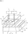
- FIG. 1 is a perspective view of the basic structure of a position measuring device with an inventively designed scale 1 shown.
- the scale 1 has a pitch which can be scanned by a scanning unit 2 located at a small distance from it.
- the graduation consists of a periodic sequence of electrically conductive dividing elements 12 spaced apart in the measuring direction X.
- the dividing elements 12 are flat and rectangular in shape, which can be divided but also others Have shapes, for example, round or triangular.
- the full-surface shape of the dividing elements 12 is not a condition, a dividing element may also be formed as a closed turn. It is only important that 12 eddy currents can form in each case in a dividing element, which act against a field of excitation emanating from the scanning unit 2.
- the scanning unit 2 is in FIG. 1 only schematically illustrated to illustrate the function of the inductive scanning in cooperation with the scale 1.
- the scanning unit 2 has at least one excitation unit, in particular in the form of a planar excitation winding 21, which is fed by a drive unit 3 with an excitation current such that a time-varying electromagnetic excitation field in the region of the dividing elements 12 is generated.
- This exciting current has, for example, a frequency of a few MHz.
- the excitation winding 21 is spatially arranged in such a way that it forms a very homogeneous electromagnetic field in the opposite sequence of the dividing elements 12.
- the scanning unit 2 furthermore has at least one detector unit, in particular in the form of a flat scanning winding 22.
- the design and spatial arrangement of the excitation winding 21 is such that in the region of the Abtastwindung 22 as homogeneous a field profile is generated.
- the Abtastwindung 22 is for this purpose within the excitation winding 21.
- the excitation field generated by the excitation winding 21 generated in the dividing elements 12 eddy currents, which act as an opposing field against the exciter field. In the Abtastwindung 22, a voltage is induced due to the exciter field associated with it, which is dependent on the relative position to the electrically conductive dividing elements 12.
- the division elements 12 are spatially arranged in the measuring direction X in such a way that they influence the field of excitation in a position-dependent manner.
- the excitation winding 21 is thus inductively coupled to the Abtastwindung 22 as a function of the relative position of the dividing elements 12 in the measuring direction X.
- the electromagnetic alternating field is determined by the Division elements 12 modulated position-dependent in the measuring direction X, thereby also varies in the Abtastwindung 22 induced voltage position dependent.
- the voltage induced in the at least one sampling winding 22 is supplied to an evaluation unit 4 which forms an electrical position-dependent signal therefrom.
- exciter winding 21 and Abtastwindung 22 in the form of applied to a common carrier 23 conductor tracks. As in FIG. 1 is shown schematically, these tracks are arranged on the side of the carrier 23, which is opposite to the sequence of the dividing elements 12 at a small sampling distance.
- the carrier 23 may be formed, for example, as a printed circuit board.
- the dividing elements 12 of the scale 1 are preferably arranged in a plane which is aligned parallel to the plane in which the excitation winding 21 and the Abtastwindung 22 extend.
- a plurality of mutually phase-shifted Abtastwindungen are usually provided in the scanning unit 2 to produce a plurality of mutually phase-shifted scanning signals, for example, by 90 ° to each other phase-shifted scanning signals.
- this embodiment is in FIG. 1 not shown.
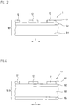
- the scale 1 is formed from a layer stack 10 which consists of a metallic composite, that is to say a sequence of metallic layers 101, 102, 103, as in FIG FIG. 2 is shown in more detail.
- This embodiment has the particular advantage that the scale 1 is particularly insensitive to ambient media during measurement operation.
- the layers 101, 102, 103 of the layer stack 10 are firmly connected to one another, ie, mutually immovable.
- the sequence of the metallic layers 101, 102, 103 of the layer stack 10 has at least one carrier layer 102, which is a ferromagnetic layer Metal is. This metal is preferably soft magnetic.
- a division layer 101 is applied, which forms after structuring the spaced apart in the measuring direction X dividing elements 12 of the scale 1.
- metals such as copper, aluminum, silver, gold or alloys containing these metals are used.
- the material of the dividing elements 12 has a high electrical conductivity, but is not ferromagnetic.
- the permeability ⁇ r of the material of the division layer 101 and thus of the dividing elements 12 is about 1.
- the layer stack 10 furthermore comprises a substrate 103, on which the sequence carrier layer 102 and division layer 101 is provided.
- This substrate 103 is dimensioned such that it decisively determines the mechanical properties of the layer stack 10.
- the thickness of the substrate 103 is a multiple, in particular 5 to 20 times, the thickness of the carrier layer 102 and a multiple of the thickness of the division layer 101.
- the thickness ratios are chosen such that the thermal expansion coefficient of the scale 1 mainly from the substrate 103rd is determined.
- the permeability of the carrier layer 102 is higher than the permeability of the substrate 103.
- the permeability ⁇ r of the metal of the carrier layer 102 is as high as possible, in particular greater than 100, advantageously greater than 1000.
- the substrate 103 stainless steel with high tensile strength and high R p0.2 proof strength, in particular stainless and hardenable stainless steel is selected. Tempering improves mechanical properties, increases dimensional stability, flexibility and toughness. If a substrate 103 is used in strip form, it can be rolled up for transport or storage due to the flexibility of the strip, without resulting in plastic deformation. By creating a firm bond of the layers 102 and 101 with the Substrate 103, these advantageous mechanical properties are transferred to the entire layer stack 10 and thus on the scale 1.
- a so-called Mu metal that is, for example, a NiFe alloy with about 80% Ni
- a substrate 103 having a thickness of 75 .mu.m to 300 .mu.m is used.
- the thickness of the carrier layer 102 is a maximum of 50 ⁇ m.
- the total thickness of the layer stack 10 is less than 1000 microns.
- the relative permeability coefficient ⁇ r of the material of the carrier layer 102 at high values is the determining variable in this respect, the magnitude of the electrical conductivity of the carrier layer 102 is secondary.
- the penetration depth ⁇ is particularly low in a material with high permeability and the material forms a high resistance to the eddy currents.
- the metallic carrier layer 102 is thus a resistance acting between the splitting layer 101 and the substrate 103 for the eddy currents. As a consequence, the eddy currents remain for the most part in the graduation elements 12 of the scale 1.
- An interfering electrically conductive connection between the dividing elements arranged in the measuring direction X 12 is no longer available for the high-frequency eddy currents.
- the arrangement of the carrier layer 102 between the division layer 101 and the substrate 103 has the advantage that, when selecting the material for the carrier layer 102, preference can be given to the magnetic properties.
- the mechanical properties of the carrier layer 102 are subordinate because the mechanical properties of the layer stack 10 are primarily determined by the substrate 103. For example, if a substrate 103 in belt form is used, the scale 1 can be rolled up for transportation or storage due to the flexibility of the belt-shaped substrate 103, without causing plastic deformation of the scale 1 is coming.
- the use of a substrate 103 determining the mechanical properties of the scale 1 now has the advantage that materials with very high permeability can be used for the carrier layer 102. In fact, these materials generally have the disadvantage that they are relatively soft and easily plastically deformable.
- the layers 101, 102, 103 of the layer stack 10 are intimately interconnected intimately by flat contact with each other, so that the layer stack 10 can be handled as a scale 1.
- a particularly advantageous method for the production is roll cladding, with which the layers 101, 102, 103 of the layer stack 10 are connected to one another inseparably.
- the roll cladding method the hot rolling method or the cold rolling method can be used.
- a highly adherent partition layer 101 is obtained on the carrier layer 102.
- an intimate planar connection is obtained between the substrate 103 and the carrier layer 102. This intimate connection ensures that the mechanical properties of the substrate 103 prevail and the further layers 101 , 102 of the layer stack 10, in particular the flexibility and the thermal expansion properties.
- the roll cladding has the advantage that particularly long scales 1 over several meters can be easily produced by the layer stack 10 is made of metal strips.
- the layer stack 10 is cold-roll cladding. It consists of a forming process in which the cleaned and possibly pretreated layers 101, 102, 103 are rolled together in the form of metal strips in the cold state, ie below the recrystallization temperature. Due to the large pressures occurring on the one hand thickness reductions of 30 to 60% are achieved and on the other hand, a fixed non-detachable bond between the individual layers 101, 102, 103 created among themselves. This intimate bond results from adhesion forces, mechanical interlocking of the surfaces and metallic bonds.
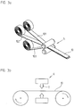
- FIG. 3a the method cold roll plating for the production of the layer stack 10 is shown schematically.
- the substrate 103, the carrier layer 102, and the partitioning layer 101 are in strip form, and are fed in common to a rolling device 5 in which they are united together under high pressure.
- an annealing treatment also called diffusion annealing or adhesion annealing
- material recrystallization takes place on the one hand, and further solidification of the compound in the bonding zones between the individual layers 101, 102, 103 on the other hand.
- FIG. 3b Such an annealing treatment of the rolled layer stack 10 is shown schematically.
- the layer stack 10 is guided through an annealing device 6, in which the layer stack is exposed to a high temperature T.
- at least one further annealing treatment follows. If steel 103 is selected as the substrate, then this steel can be hardened in a further annealing treatment.
- an annealing treatment can serve to improve the magnetic properties, such. B. to optimize the permeability of the carrier layer 102.
- multiple rolling and annealing processes can be performed sequentially to achieve the desired parameters of the layer stack 10.
- the layer stack 10 thus formed can then be further processed as a composite. If necessary, a surface treatment can be carried out and the composite can be made by cutting to the required dimensions, for example.
- the dividing elements 12 are formed from the dividing layer 101 by known structuring methods, such as a photochemical etching process.
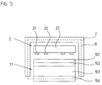
- a compensation layer 104 is applied to the rear side of the substrate 103, which should avoid bending of the substrate 103, caused by the one-sided coating with the carrier layer 102 and the division layer 101.
- a curvature introduced by the carrier layer 102, caused by the bimetallic effect is thereby to be prevented or at least largely avoided.
- the compensation layer 104 applied to the rear side of the substrate 103 advantageously also consists of the same material as the carrier layer 102.
- the thickness of the compensation layer 104 is selected such that a curvature of the substrate 103 is avoided.
- the thickness ratios are also preferably selected such that the mechanical properties and the thermal expansion coefficient of the scale 1.1 are predominantly determined by the substrate 103.
- the layer stack 10.1 consisting of the division layer 101, the carrier layer 102, the substrate 103 and the compensation layer 104, in turn together by a rolling process, in particular the cold rolling process, are joined together to form an intimate composite.
- the compensation layer 104 on the back side of the substrate 103 may be additionally used to shield the position measuring device from external magnetic noise.
- the shield 7 consists of a flux-conducting material, in particular soft magnetic material, so that together with the compensation layer 104, an at least substantially closed magnetic circuit 8 is formed.
- the shield 7 surrounds the scanning unit and the scale 1.1 U-shaped on three sides.
- the shield 7 extends over the ferromagnetic carrier layer 102 and extends at least substantially to the compensation layer 104.
- the scale 1 or 1.1 can be additionally protected against environmental influences by providing at least the upper side of the scale 1 or 1.1 with a protective layer.
- This protective layer may be a lacquer layer, a powder coating, a DLC layer or a metal layer.
- the invention is explained by way of example with reference to a single-track incremental scale 1 or 1.1.
- the invention can also be implemented in multi-track incremental as well as absolute scales.
- An absolute scale can be executed in one lane in the form of a so-called PRC code or chain code, as a multi-lane code with a plurality of juxtaposed incremental tracks of different graduation period, for example in the form of a Gray code or as a so-called Vernier system with a plurality of juxtaposed incremental tracks with only slightly different graduation periods.
Description
Die vorliegende Erfindung betrifft einen Maßstab mit einer induktiv abtastbaren Teilung sowie eine Positionsmesseinrichtung mit diesem Maßstab.The present invention relates to a scale with an inductively scannable graduation and a position measuring device with this scale.
Positionsmesseinrichtungen, die nach dem induktiven Messprinzip arbeiten, weisen einen Maßstab auf, der eine induktiv abtastbare Teilung besitzt. Die Teilung besteht aus einer Abfolge voneinander beabstandeter elektrisch leitfähiger Teilungselemente. Die Teilung wird im Messbetrieb von einer Abtasteinheit abgetastet, die zumindest eine Erregerwindung und eine Abtastwindung aufweist. Diese Windungen sind vorzugsweise flächig auf einer Leiterplatte aufgebracht. Ein an der Erregerwindung eingeprägter Erregerstrom generiert ein zeitlich wechselndes elektromagnetisches Erregerfeld, das durch die Anordnung der Teilungselemente positionsabhängig beeinflusst wird, wodurch in der Abtastwindung ein positionsabhängiges Abtastsignal induziert wird.Position measuring devices that operate on the inductive measuring principle, have a scale that has an inductively scannable division. The division consists of a sequence of spaced-apart electrically conductive dividing elements. The division is scanned in the measurement mode by a scanning unit, which has at least one excitation winding and a Abtastwindung. These windings are preferably applied flat on a circuit board. An exciter current impressed on the excitation winding generates a temporally alternating electromagnetic exciter field which is influenced position-dependent by the arrangement of the graduation elements, whereby a position-dependent scanning signal is induced in the Abtastwindung.
Induktiv abtastbare Maßstäbe und induktiv arbeitende Positionsmesseinrichtungen haben den Vorteil, dass sie relativ unempfindlich gegenüber Verschmutzungen sind. Sie sind insbesondere unempfindlich gegenüber Flüssigkeiten wie Wasser und Öle im Raum zwischen Maßstab und Abtasteinheit, weshalb sie sich besonders zur Winkel- und Längenmessung an Werkzeugmaschinen eignen.Inductive scannable scales and inductive position measuring devices have the advantage that they are relatively insensitive to contamination. They are particularly insensitive to liquids such as water and oils in the space between scale and scanning unit, which is why they are particularly suitable for measuring the angle and length of machine tools.
In der
Als Bedingung für die Verwendung eines Metallträgers wird in der
Aufgabe der vorliegenden Erfindung ist es daher, einen induktiv abtastbaren Maßstab anzugeben, der auch in relativ großen Längen einfach herstellbar ist, unempfindlich gegenüber Umgebungseinflüssen ist und bei der induktiven Abtastung gut auswertbare, also hohe Abtastsignale generiert.Object of the present invention is therefore to provide an inductively scannable scale, which can be easily produced even in relatively large lengths is insensitive to environmental influences and in the inductive scanning well evaluable, ie generates high scanning signals.
Diese Aufgabe wird erfindungsgemäß durch einen Maßstab mit den Merkmalen des Anspruchs 1 gelöst.This object is achieved by a scale with the features of
Der erfindungsgemäß ausgebildete Maßstab weist zumindest eine in Messrichtung verlaufende induktiv abtastbare Teilung auf, die aus einer in Messrichtung angeordneten Folge voneinander beabstandeter elektrisch leitfähiger Teilungselemente besteht. Die Teilungselemente sind derart ausgebildet, dass sich jeweils in einem Teilungselement Wirbelströme ausbilden können, die bei der Abtastung gegen ein von einer Abtasteinheit ausgehendes Erregerfeld wirken. Der Maßstab umfasst einen Schichtstapel, der ausschließlich aus einer Abfolge von metallischen Schichten besteht, wobei diese Abfolge von metallischen Schichten zumindest eine Trägerschicht und eine die Teilungselemente bildende Teilungsschicht aufweist. Die Trägerschicht ist zwischen der Teilungsschicht und einem metallischen Substrat angeordnet und besteht aus einem ferromagnetischen, insbesondere auch weichmagnetischen, Metall. Das Substrat ist derart dimensioniert, dass es maßgebend die mechanischen Eigenschaften des Schichtstapels bestimmt, indem die Dicke des Substrats ein Vielfaches der Dicke der Trägerschicht beträgt.The scale formed according to the invention has at least one inductive scanning graduation running in the measuring direction, which consists of a series of spaced-apart, electrically conductive dividing elements arranged in the measuring direction. The dividing elements are designed in such a way that eddy currents can form in each case in a dividing element, which eddy currents act during the scanning against an exciting field emanating from a scanning unit. The scale comprises a layer stack consisting exclusively of a sequence of metallic layers, this sequence of metallic layers having at least one carrier layer and a division layer forming the dividing elements. The carrier layer is arranged between the division layer and a metallic substrate and consists of a ferromagnetic, in particular also soft magnetic, metal. The substrate is dimensioned such that it decisively determines the mechanical properties of the layer stack by the thickness of the substrate being a multiple of the thickness of the carrier layer.
Aus der
Einen ähnlichen Aufbau findet man in der
Vorzugsweise ist gemäß der Erfindung das Material der Trägerschicht ein ferromagnetisches Metall mit einer Permeabilität µr größer 100, besonders vorteilhaft ist die Verwendung eines Metalls mit einer Permeabilität µr größer 1000. Geeignete ferromagnetische Metalle sind insbesondere Mu-Metalle, dieses sind weichmagnetische Nickel-Eisen-Legierungen mit einem Nickelanteil von etwa 70-80%. Mu-Metalle werden unter dem Handelsnamen Mumetall vertrieben. Anstelle von Nickel-Eisen-Legierungen können auch andere Legierungen oder auch ferritische Stähle mit einer relativ hohen Permeabilität, insbesondere größer 100, Verwendung finden.Preferably, according to the invention, the material of the carrier layer is a ferromagnetic metal having a permeability μ r greater than 100, particularly advantageous is the use of a metal having a permeability μ r greater than 1000. Suitable ferromagnetic metals are in particular Mu metals, these are soft magnetic nickel-iron Alloys with a nickel content of about 70-80%. Mu metals are sold under the trade name Mumetall. Instead of nickel-iron alloys, other alloys or even ferritic steels with a relatively high permeability, in particular greater than 100, can be used.
Bei der Erfindung wird die Tatsache ausgenutzt, dass bei der induktiven Abtastung Wechselfelder generiert werden und für die Effizienz eines Maßstabs nicht allein die elektrische Leitfähigkeit der Trägerschicht bedeutend ist, auf der die Teilungselemente aufgebracht sind. Ebenso bedeutend ist die Permeabilität des als Trägerschicht verwendeten Materials. Bei der Erfindung wird die von der Permeabilität des verwendeten Materials frequenzabhängige Eindringtiefe von Wirbelströmen genutzt. Vor allem bei hochpermeablen Werkstoffen ist die Eindringtiefe nämlich besonders klein. Je geringer die Eindringtiefe, desto höher ist der wirksame Widerstand für Wirbelströme. Störende Wirbelströme, die sich von einem Teilungselement zu einem daneben angeordneten Teilungselement ausbilden, können somit unterdrückt werden. Bei der Verwendung von ferromagnetischen Metallen hoher Permeabilität spielt die elektrische Leitfähigkeit des Metalls eine untergeordnete Rolle.In the invention, the fact is exploited that are generated in the inductive sensing AC fields and for the efficiency of a scale not only the electrical conductivity of the support layer is significant, on which the dividing elements are applied. Equally important is the permeability of the material used as a carrier layer. In the invention, the permeability of the material used frequency-dependent penetration depth of eddy currents is used. Especially with high-permeability materials, the penetration depth is particularly small. The lower the penetration depth, the higher the effective resistance to eddy currents. Disturbing eddy currents, which form from a dividing element to a dividing element arranged next to it, can thus be suppressed. When using ferromagnetic metals of high permeability, the electrical conductivity of the metal plays a minor role.
Die Permeabilität der Trägerschicht ist höher als die Permeabilität des Substrats.The permeability of the carrier layer is higher than the permeability of the substrate.
Als Substrat wird vorzugsweise ein Edelstahl verwendet. Damit das Substrat maßgebend die mechanischen Eigenschaften des gesamten Schichtstapels und somit des Maßstabs bestimmt, beträgt die Dicke des Substrats ein Vielfaches der Dicke der Trägerschicht, insbesondere beträgt die Dicke des Substrats mehr als das 5 bis 20-fache der Dicke der Trägerschicht.As the substrate, a stainless steel is preferably used. So that the substrate decisively determines the mechanical properties of the entire layer stack and thus of the scale, the thickness of the substrate is a multiple of the thickness of the carrier layer, in particular the thickness of the substrate is more than 5 to 20 times the thickness of the carrier layer.
Durch das Vorsehen eines relativ dicken Substrats für die Schichtenfolge Trägerschicht und Teilungsschicht, wird dem Verbund aus allen Schichten die mechanische Eigenschaft des Substrats aufgeprägt. Durch diese Maßnahme können für die Trägerschicht Materialien mit sehr hoher Permeabilität eingesetzt werden, die dann auch relativ weich und mechanisch instabil sein können.By providing a relatively thick substrate for the layer sequence carrier layer and division layer, the composite of all layers is impressed on the mechanical property of the substrate. By this measure, materials with very high permeability can be used for the carrier layer, which can then be relatively soft and mechanically unstable.
Die Materialien und Dickenverhältnisse werden vorzugsweise derart gewählt, dass der Schichtstapel und somit der Maßstab einen resultierenden thermischen Ausdehnungskoeffizienten hat, der nur unwesentlich vom thermischen Ausdehnungskoeffizienten des Substrats abweicht, insbesondere nur um einen Wert von maximal ±1×10⁻⁶K-1 abweicht. Vorzugsweise hat das Substrat einen thermischen Ausdehnungskoeffizienten von etwa 10×10-6K-1 und der Maßstab somit einen resultierenden thermischen Ausdehnungskoeffizienten von etwa 9×10⁻⁶K-1 bis 11×10-6K-1.The materials and thickness ratios are preferably chosen such that the layer stack and thus the scale has a resulting coefficient of thermal expansion, which deviates only insignificantly from the thermal expansion coefficient of the substrate, in particular only by a value of ± 1 × 10 -6 K -1 . Preferably, the substrate has a thermal expansion coefficient of about 10 × 10 -6 K -1, and thus the scale has a resulting coefficient of thermal expansion of about 9 × 10 -6 K -1 to 11 × 10 -6 K -1 .
In einer bevorzugten Ausgestaltung ist auf einer Seite des Substrats die Schichtenfolge Trägerschicht und Teilungsschicht vorgesehen und auf der anderen Seite des Substrats zumindest eine Kompensationsschicht, die einer Krümmung des Schichtstapels hervorgerufen durch den Bimetalleffekt entgegenwirkt. Diese Kompensationsschicht besteht vorzugsweise aus dem gleichen Metall wie die Trägerschicht, insbesondere auch aus einem ferromagnetischen Metall, das insbesondere eine Permeabilität µr größer 100, vorzugsweise größer 1000 aufweist.In a preferred embodiment, the layer sequence carrier layer and division layer is provided on one side of the substrate and on the other side of the substrate at least one compensation layer, which counteracts a curvature of the layer stack caused by the bimetallic effect. This compensation layer preferably consists of the same metal as the carrier layer, in particular also of a ferromagnetic metal, which in particular has a permeability μ r greater than 100, preferably greater than 1000.
Einen besonders innigen und stabilen Verbund der Schichten des Schichtstapels erhält man, wenn diese mittels Walzplattieren, insbesondere Kaltwalzplattleren, miteinander verbunden sind.A particularly intimate and stable composite of the layers of the layer stack is obtained when these are connected to one another by means of roll cladding, in particular cold roll plate sliders.
Ein derartiger Maßstab kann für Positionsmesseinrichtungen in Form von Winkelmesseinrichtungen und Längenmesseinrichtungen eingesetzt werden. Da ein derart aufgebauter Maßstab auch in Bandform leicht herstellbar ist, eignet er sich besonders für Längenmesseinrichtungen großer Länge. Ein erfindungsgemäß aufgebauter Maßstab in Bandform kann auch in vorteilhafter Weise in Winkelmesseinrichtungen eingesetzt werden, wenn er beispielsweise auf den Innen- oder Außenumfang einer Trommel aufgebracht wird. Zum klebenden Aufbringen des erfindungsgemäß ausgebildeten Maßstabs kann der Schichtstapel auf der Unterseite durch ein Klebemittel ergänzt sein, insbesondere ein Klebeband, das zur guten Handhabung als doppelseitiges Klebeband ausgeführt sein kann.Such a scale can be used for position measuring devices in the form of angle measuring devices and length measuring devices. Since a scale constructed in this way can also be produced easily in strip form, it is particularly suitable for length measuring devices great length. An inventively constructed scale in strip form can also be used advantageously in angle measuring devices when it is applied, for example, to the inner or outer circumference of a drum. For adhesive application of the scale formed according to the invention, the layer stack on the underside can be supplemented by an adhesive, in particular an adhesive tape which can be designed for good handling as a double-sided adhesive tape.
Mit der Erfindung soll weiterhin eine Positionsmesseinrichtung angegeben werden, die relativ unempfindlich gegen Umgebungseinflüsse ist und die gut auswertbare Abtastsignale generiert.With the invention, a position measuring device is still to be specified, which is relatively insensitive to environmental influences and generates the well-evaluable scanning signals.
Eine derartige Positionsmesseinrichtung ist im Anspruch 11 angegeben. Die Positionsmesseinrichtung weist demnach einen Maßstab mit einer in Messrichtung verlaufenden induktiv abtastbaren Teilung auf, die aus einer in Messrichtung angeordneten Folge voneinander beabstandeter Teilungselemente besteht. Dieser Maßstab umfasst einen Schichtstapel, der ausschließlich aus einer Abfolge von metallischen Schichten besteht, wobei diese Abfolge von metallischen Schichten zumindest eine Trägerschicht und eine die Teilungselemente bildende Teilungsschicht aufweist. Die Trägerschicht ist zwischen der Teilungsschicht und einem metallischen Substrat angeordnet und ist ein ferromagnetisches Metall. Die Permeabilität der Trägerschicht ist höher als die Permeabilität des Substrats, das Material der Trägerschicht weist insbesondere eine Permeabilität µr größer 100, vorzugsweise größer 1000 auf. Das Substrat ist derart dimensioniert, dass es die mechanischen Eigenschaften des Schichtstapels maßgebend bestimmt. Die Positionsmesseinrichtung umfasst ferner eine Abtasteinheit zur Abtastung der Teilung des Maßstabs, wobei die Abtasteinheit eine Erregereinheit zur Erzeugung eines elektromagnetischen Wechselfeldes und eine Detektoreinheit zur Detektion des von den Teilungselementen positionsabhängig modulierten elektromagnetischen Wechselfeldes aufweist.Such a position-measuring device is specified in claim 11. The position-measuring device accordingly has a scale with an inductive scanning graduation running in the measuring direction, which consists of a spacing of spaced-apart dividing elements arranged in the measuring direction. This scale comprises a layer stack consisting exclusively of a sequence of metallic layers, this sequence of metallic layers having at least one carrier layer and a division layer forming the dividing elements. The support layer is disposed between the split layer and a metallic substrate and is a ferromagnetic metal. The permeability of the carrier layer is higher than the permeability of the substrate, the material of the carrier layer in particular has a permeability μ r greater than 100, preferably greater than 1000. The substrate is dimensioned such that it decisively determines the mechanical properties of the layer stack. The position measuring device further comprises a scanning unit for scanning the graduation of the scale, wherein the scanning unit has an excitation unit for generating an electromagnetic alternating field and a detector unit for detecting the positionally modulated by the dividing elements electromagnetic alternating field.
Die Erregereinheit wird vorzugsweise von zumindest einer flächigen Erregerwindung und die Detektoreinheit von zumindest einer flächigen Abtastwindung gebildet.The excitation unit is preferably formed by at least one planar excitation winding and the detector unit by at least one flat Abtastwindung.
In einer besonders vorteilhaften Ausgestaltung ist auf einer Seite des Substrats die Schichtenfolge Trägerschicht und Teilungsschicht vorgesehen und auf der anderen Seite des Substrats zumindest eine Kompensationsschicht, die vorzugsweise aus dem gleichen Material wie die Trägerschicht besteht und ein ferromagnetisches Metall ist. Die Abtasteinheit weist eine sie umgebende Abschirmung auf, wobei die Abschirmung derart ausgebildet ist, dass diese mit der Kompensationsschicht einen geschlossenen Magnetkreis ausbildet. Hierzu ist die Permeabilität µr des Metalls der Kompensationsschicht insbesondere größer 100, vorzugsweise größer 1000.In a particularly advantageous embodiment, the layer sequence carrier layer and division layer is provided on one side of the substrate and on the other side of the substrate at least one compensation layer, which preferably consists of the same material as the carrier layer and is a ferromagnetic metal. The scanning unit has a surrounding shield, wherein the shield is formed such that it forms a closed magnetic circuit with the compensation layer. For this purpose, the permeability μ r of the metal of the compensation layer is in particular greater than 100, preferably greater than 1000.
Alle Angaben zur Permeabilität beziehen sich auf den Betrieb der Positionsmesseinrichtung, also bei einer Frequenz des Erregerstroms von größer 1 MHz.All information on the permeability relate to the operation of the position measuring device, ie at a frequency of the excitation current of greater than 1 MHz.
Vorteile sowie Einzelheiten der vorliegenden Erfindung ergeben sich aus der nachfolgenden Beschreibung von Ausführungsbeispielen anhand der beiliegenden Figuren.Advantages and details of the present invention will become apparent from the following description of exemplary embodiments with reference to the accompanying figures.
Es zeigen
Figur 1- eine perspektivische Ansicht einer induktiven Positionsmesseinrichtung;
Figur 2- den Maßstab der Positionsmesseinrichtung gemäß
Figur 1 ; - Figur 3a
- einen ersten Verfahrensschritt zur Herstellung des Maßstabs;
- Figur 3b
- einen zweiten Verfahrensschritt zur Herstellung des Maßstabs;
- Figur 4
- eine weitere Ausgestaltung eines Maßstabs gemäß der Erfindung und
Figur 5- eine Positionsmesseinrichtung mit dem in
Figur 4 dargestellten Maßstab.
- FIG. 1
- a perspective view of an inductive position measuring device;
- FIG. 2
- the scale of the position measuring device according to
FIG. 1 ; - FIG. 3a
- a first process step for the production of the scale;
- FIG. 3b
- a second process step for the production of the scale;
- FIG. 4
- a further embodiment of a scale according to the invention and
- FIG. 5
- a position measuring device with the in
FIG. 4 scale shown.
In
Die Abtasteinheit 2 ist in
Die Abtasteinheit 2 weist darüber hinaus zumindest eine Detektoreinheit insbesondere in Form einer flächigen Abtastwindung 22 auf. Die Ausführung und räumliche Anordnung der Erregerwindung 21 ist derart, dass in dem Bereich der Abtastwindung 22 ein möglichst homogener Feldverlauf erzeugt wird. Die Abtastwindung 22 befindet sich hierzu innerhalb der Erregerwindung 21. Das von der Erregerwindung 21 generierte Erregerfeld generiert in den Teilungselementen 12 Wirbelströme, die als Gegenfeld gegen das Erregerfeld wirken. In der Abtastwindung 22 wird aufgrund des ihr zugeordneten Erregerfeldes eine Spannung induziert, die von der relativen Lage zu den elektrisch leitenden Teilungselementen 12 abhängig ist. Die Teilungselemente 12 sind in Messrichtung X räumlich derart angeordnet, dass sie das Erregerfeld positionsabhängig beeinflussen. Die Erregerwindung 21 ist also mit der Abtastwindung 22 in Abhängigkeit der relativen Lage der Teilungselemente 12 in Messrichtung X induktiv gekoppelt. Das elektromagnetische Wechselfeld wird durch die Teilungselemente 12 in Messrichtung X positionsabhängig moduliert, dadurch variiert auch die in der Abtastwindung 22 induzierte Spannung positionsabhängig. Die in der zumindest einen Abtastwindung 22 induzierte Spannung wird einer Auswerteeinheit 4 zugeführt, die daraus ein elektrisches positionsabhängiges Signal bildet.The
Besonders vorteilhaft ist die Anordnung von Erregerwindung 21 und Abtastwindung 22 in Form von auf einem gemeinsamen Träger 23 aufgebrachten Leiterbahnen. Wie in
In nicht gezeigter Weise sind üblicherweise mehrere gegeneinander phasenversetzte Abtastwindungen in der Abtasteinheit 2 vorgesehen, um mehrere gegeneinander phasenverschobene Abtastsignale zu erzeugen, beispielsweise um 90° gegeneinander phasenverschobene Abtastsignale. Aus Gründen der Übersichtlichkeit ist diese Ausgestaltung in
Der Maßstab 1 ist aus einem Schichtstapel 10 gebildet, der aus einem metallischen Verbund, also aus einer Abfolge von metallischen Schichten 101, 102, 103 besteht, wie in
Die Abfolge der metallischen Schichten 101, 102, 103 des Schichtstapels 10 weist zumindest eine Trägerschicht 102 auf, die ein ferromagnetisches Metall ist. Dieses Metall ist vorzugsweise weichmagnetisch. Auf dieser durchgehenden Trägerschicht 102 ist eine Teilungsschicht 101 aufgebracht, welche nach erfolgter Strukturierung die in Messrichtung X voneinander beabstandeten Teilungselemente 12 des Maßstabs 1 bildet. Als Material für diese Teilungselemente 12 werden Metalle wie beispielsweise Kupfer, Aluminium, Silber, Gold oder diese Metalle enthaltende Legierungen verwendet. Das Material der Teilungselemente 12 weist eine hohe elektrische Leitfähigkeit auf, ist jedoch nicht ferromagnetisch. Die Permeabilität µr des Materials der Teilungsschicht 101 und somit der Teilungselemente 12 liegt bei etwa 1.The sequence of the
Der Schichtstapel 10 umfasst weiterhin ein Substrat 103, auf dem die Abfolge Trägerschicht 102 und Teilungsschicht 101 vorgesehen ist. Dieses Substrat 103 ist derart dimensioniert, dass es die mechanischen Eigenschaften des Schichtstapels 10 maßgebend bestimmt. Hierzu beträgt die Dicke des Substrats 103 ein Vielfaches, insbesondere das 5- bis 20-fache, der Dicke der Trägerschicht 102 sowie ein Vielfaches der Dicke der Teilungsschicht 101. Die Dickenverhältnisse werden derart gewählt, dass der thermische Ausdehnungskoeffizient des Maßstab 1 vorwiegend vom Substrat 103 bestimmt wird.The
Die Permeabilität der Trägerschicht 102 ist höher als die Permeabilität des Substrats 103. Die Permeabilität µr des Metalls der Trägerschicht 102 ist möglichst hoch, insbesondere größer 100, vorteilhafterweise größer 1000.The permeability of the
Als Material für das Substrat 103 ist rostfreier Edelstahl mit hoher Zugfestigkeit und hoher Rp0.2-Dehngrenze, insbesondere rostfreier und härtbarer Edelstahl gewählt. Durch Vergüten werden die mechanischen Eigenschaften verbessert, die Formstabilität, die Flexibilität und die Zähigkeit werden erhöht. Wird ein Substrat 103 in Bandform verwendet, kann dieses zum Transport oder zur Lagerung aufgrund der Flexibilität des Bandes aufgerollt werden, ohne dass es zu plastischen Verformungen kommt. Durch die Schaffung eines festen Verbundes der Schichten 102 und 101 mit dem Substrat 103 werden diese vorteilhaften mechanischen Eigenschaften auf den gesamten Schichtstapel 10 und somit auf den Maßstab 1 übertragen.As a material for the
Die unmittelbar unterhalb der Teilungselemente 12 angeordnete und durchgehende Trägerschicht 102 aus einem Material mit hoher Permeabilität hat den Vorteil, dass störende Wirbelströme, die sich von einem Teilungselement 12 zu einem daneben angeordneten Teilungselement 12 ausbilden, zumindest weitgehend unterdrückt werden. Voraussetzung dafür ist, dass die Dicke der Trägerschicht 102 abhängig vom gewählten Material ausreichend groß gewählt wird. Die Dicke soll ein Vielfaches, beispielsweise das 5-fache, der Eindringtiefe δ der Wirbelströme betragen: ![]()
- mit
- δ = Eindringtiefe (Tiefe, bei der der Strom auf ca. 37% des Oberflächenwertes gefallen ist)
- σ = spezifischer elektrischer Widerstand des Materials
- f = Frequenz
- µ0 = Permeabilitätskonstante des Vakuums
- µr = relative Permeabilitätszahl des Materials
- With
- δ = penetration depth (depth at which the current has fallen to approx. 37% of the surface value)
- σ = specific electrical resistance of the material
- f = frequency
- μ 0 = permeability constant of the vacuum
- μ r = relative permeability of the material
Wird beispielsweise als Trägerschicht 102 ein sogenanntes Mu-Metall, also beispielsweise eine NiFe-Legierung mit etwa 80% Ni verwendet, gelten folgende Dimensionierungsregeln: ![]()
spezifischer elektrischer Widerstand: 0,55µΩm
Relevanter Frequenzbereich: 1MHz bis 10MHz (Beispielfrequenzen)If, for example, a so-called Mu metal, that is, for example, a NiFe alloy with about 80% Ni, is used as the ![]()
specific electrical resistance: 0.55μΩm
Relevant frequency range: 1MHz to 10MHz (sample frequencies)
Abhängig von der daraus errechneten Eindringtiefe δ ergibt sich eine optimale Dicke der Trägerschicht 102:
- Eindringtiefe δ bei 1MHz = 5,3µm
=> optimale Dicke ≈ 27µm (5-fache Eindringtiefe δ) - Eindringtiefe δ bei 10MHz = 1,7µm
=> optimale Dickes ≈ 9µm (5-fache Eindringtiefe ö)
- Penetration depth δ at 1MHz = 5.3μm
=> optimal thickness ≈ 27μm (5 times the penetration depth δ) - Penetration depth δ at 10MHz = 1.7μm
=> optimal thickness ≈ 9μm (5 times the penetration depth ö)
Bei einer Dicke der Trägerschicht 102 von etwa 15 µm wird ein Substrat 103 mit einer Dicke von 75 µm bis 300 µm verwendet.With a thickness of the
Bei einem einfach - insbesondere durch Walzplattieren - herstellbaren Maßstab 1 in Bandform, der auch gut handhabbar ist, beträgt die Dicke der Trägerschicht 102 maximal 50 µm. Die Gesamtdicke des Schichtstapels 10 ist kleiner 1000 µm.In the case of a
Da die relative Permeabilitätszahl µr des Materials der Trägerschicht 102 bei hohen Werten diesbezüglich die bestimmende Größe ist, ist die Größe der elektrischen Leitfähigkeit der Trägerschicht 102 nachrangig. Die Eindringtiefe ö ist in einem Material mit hoher Permeabilität besonders gering und das Material bildet für die Wirbelströme einen hohen Widerstand. Die metallische Trägerschicht 102 ist somit ein für die Wirbelströme wirkender Widerstand zwischen der Teilungsschicht 101 und dem Substrat 103. Als Folge verbleiben die Wirbelströme zum größten Teil in den Teilungselementen 12 des Maßstabs 1. Eine störende elektrisch leitfähige Verbindung zwischen den in Messrichtung X voneinander angeordneten Teilungselementen 12 liegt für die hochfrequenten Wirbelströme nicht mehr vor.Since the relative permeability coefficient μ r of the material of the
Die Anordnung der Trägerschicht 102 zwischen der Teilungsschicht 101 und dem Substrat 103 hat den Vorteil, dass bei der Auswahl des Materials für die Trägerschicht 102 vorrangig auf die magnetischen Eigenschaften geachtet werden kann. Die mechanischen Eigenschaften der Trägerschicht 102 sind nachrangig, da die mechanischen Eigenschaften des Schichtstapels 10 vorrangig vom Substrat 103 bestimmt werden. Wird beispielsweise ein Substrat 103 in Bandform verwendet, kann der Maßstab 1 zum Transport oder zur Lagerung aufgrund der Flexibilität des bandförmigen Substrats 103 aufgerollt werden, ohne dass es zu plastischen Verformungen des Maßstabs 1 kommt. Die Verwendung eines die mechanischen Eigenschaften des Maßstabs 1 bestimmenden Substrats 103 hat nun den Vorteil, dass für die Trägerschicht 102 Materialien mit sehr hoher Permeabilität eingesetzt werden können. Diese Materialien haben nämlich in der Regel den Nachteil, dass sie relativ weich und leicht plastisch verformbar sind.The arrangement of the
Die Schichten 101, 102, 103 des Schichtstapels 10 sind innig durch flächigen Kontakt zueinander unverrückbar miteinander verbunden, so dass der Schichtstapel 10 als Maßstab 1 handhabbar ist. Ein besonders vorteilhaftes Verfahren zur Herstellung ist das Walzplattieren, mit dem die Schichten 101, 102, 103 des Schichtstapels 10 untrennbar miteinander verbunden werden. Als Walzplattierverfahren kann das Warmwalzverfahren oder das Kaltwalzverfahren eingesetzt werden. Als Ergebnis erhält man eine bestens haftende Teilungsschicht 101 auf der Trägerschicht 102. Darüber hinaus erhält man eine innige flächige Verbindung zwischen dem Substrat 103 und der Trägerschicht 102. Diese innige Verbindung gewährleistet, dass die mechanischen Eigenschaften des Substrats 103 vorherrschen und auf die weiteren Schichten 101, 102 des Schichtstapels 10 übertragen werden, insbesondere die Flexibilität und die thermischen Ausdehnungseigenschaften. Das Walzplattieren hat den Vorteil, dass besonders lange Maßstäbe 1 über mehrere Meter einfach hergestellt werden können, indem der Schichtstapel 10 aus Metallbändern hergestellt wird.The
Zur Bildung des Schichtstapels 10 besonders geeignet ist das Kaltwalzplattieren. Es besteht aus einem Umformprozess, bei dem die gereinigten und ggf. vorbehandelten Schichten 101, 102, 103 in Form von Metallbändern gemeinsam in kaltem Zustand, also unterhalb der Rekristallisationstemperatur, gewalzt werden. Aufgrund der dabei auftretenden großen Drücke werden einerseits Dickenreduzierungen von 30 bis 60% erzielt und andererseits wird ein fester unlösbarer Verbund zwischen den einzelnen Schichten 101, 102, 103 untereinander geschaffen. Dieser innige Verbund resultiert aus Adhäsionskräften, mechanischen Verklammerungen der Oberflächen und metallischen Bindungen.Particularly suitable for forming the
In
Nach dem eigentlichen Walzvorgang schließt sich eine Glühbehandlung, auch Diffusionsglühen oder Haftungsglühen genannt, an. Bei dieser Wärmebehandlung erfolgt einerseits eine Materialrekristallisation und andererseits in den Verbindungszonen zwischen den einzelnen Schichten 101, 102, 103 eine weitere Verfestigung der Verbindung. In
Bei Bedarf können mehrere Walz- und Glühprozesse aufeinanderfolgend durchgeführt werden, um die gewünschten Parameter des Schichtstapels 10 zu erreichen.If desired, multiple rolling and annealing processes can be performed sequentially to achieve the desired parameters of the
Der so gebildete Schichtstapel 10 lässt sich danach als Verbund weiter verarbeiten. Wenn erforderlich, kann eine Oberflächenbehandlung erfolgen und der Verbund kann beispielsweise durch Zuschnitt auf die erforderlichen Abmessungen gebracht werden. Die Teilungselemente 12 werden durch bekannte Strukturierungsverfahren, wie beispielsweise einen photochemischen Ätzprozess, aus der Teilungsschicht 101 gebildet..The
Nachfolgend wird eine weitere Ausgestaltung eines Maßstabs 1.1 erläutert. Zur Reduzierung von thermischen Verbiegungen des Maßstabs 1.1 ist ein symmetrischer Schichtaufbau des Schichtstapels 10.1 von besonderem Vorteil. Ein Beispiel dazu ist in
Besonders vorteilhaft ist es, wenn der Schichtstapel 10.1, bestehend aus der Teilungsschicht 101, der Trägerschicht 102, dem Substrat 103 und der Kompensationsschicht 104, wiederum gemeinsam durch ein Walzverfahren, insbesondere das Kaltwalzverfahren, zu einem innigen Verbund zusammengefügt werden.It is particularly advantageous if the layer stack 10.1, consisting of the
Wie in
Sollte es für bestimmte Anwendungen erforderlich sein, so kann der Maßstab 1 bzw. 1.1 zusätzlich vor Umwelteinflüssen geschützt werden, indem zumindest die Oberseite des Maßstabs 1 bzw. 1.1 mit einer Schutzschicht versehen wird. Diese Schutzschicht kann eine Lackschicht, eine Pulverbeschichtung, eine DLC-Schicht oder eine Metallschicht sein.Should it be necessary for certain applications, the
Die Erfindung ist beispielhaft anhand eines einspurigen inkrementalen Maßstabs 1 bzw. 1.1 erläutert. Die Erfindung ist auch bei mehrspurigen inkrementalen sowie bei absoluten Maßstäben realisierbar. Ein absoluter Maßstab kann dabei einspurig in Form eines sogenannten PRC-Codes oder Kettencodes ausgeführt sein, als mehrspuriger Code mit mehreren nebeneinander angeordneten Inkrementalspuren unterschiedlicher Teilungsperiode, beispielsweise in Form eines Gray-Codes oder als sogenanntes Vernier-System mit mehreren nebeneinander angeordneten Inkrementalspuren mit nur geringfügig unterschiedlichen Teilungsperioden.The invention is explained by way of example with reference to a single-track
Claims (13)
- Scale having a graduation that can be sensed inductively, comprising a sequence of electrically conductive graduation elements (12) arranged in the measuring direction (X) and spaced apart from one another, which are formed in such a way that in each case eddy currents are able to form in a graduation element (12), which currents during the sensing act relative to an excitation field originating from a sensor unit (2), the scale (1, 1.1) comprising a layer stack (10, 10.1) which comprises a sequence of metallic layers (101, 102, 103, 104), and that this sequence of metallic layers (101, 102, 103, 104) has at least one carrier layer (102) and a graduation layer (101) forming the graduation elements (12),
wherein
the carrier layer (102) is arranged between the graduation layer (101) and a metallic substrate (103), wherein the substrate (103) is dimensioned in such a way that it definitively determines the mechanical properties of the layer stack (10, 10.1) in that the thickness of the substrate (103) is a multiple of the thickness of the carrier layer (102), and
wherein the carrier layer (102) is a ferromagnetic metal. - Scale according to Claim 1, wherein the permeability of the carrier layer (102) is greater than the permeability of the substrate (103).
- Scale according to Claim 1 or 2, wherein the material of the carrier layer (102) is a soft magnetic metal.
- Scale according to one of the preceding claims, wherein the material of the carrier layer (102) is a metal with a permeability µR greater than 100, in particular greater than 1000.
- Scale according to one of the preceding claims, wherein the material of the graduation layer (101) has a permeability µR of approximately 1, in particular contains at least one of the metals copper, aluminium, gold or silver.
- Scale according to one of the preceding claims, wherein the substrate (103) consists of stainless steel.
- Scale according to one of the preceding claims, wherein the layer sequence comprising carrier layer (102) and graduation layer (101) is provided on one side of the substrate, and wherein at least one compensation layer (104), which counteracts a deflection of the layer stack (10, 10.1) brought about by the bimetal effect, is provided on the other side of the substrate (103).
- Scale according to Claim 7, wherein the compensation layer (104) consists of a ferromagnetic metal.
- Scale according to one of the preceding claims, wherein the layers (101, 102, 103, 104) of the layer stack (10.1) are connected to one another by means of roll cladding.
- Scale according to Claim 9, wherein the layers (101, 102, 103, 104) of the layer stack (10, 10.1) are connected to one another by means of cold roll cladding.
- Position measuring device having a scale (1, 1.1) according to one of the preceding claims and having a sensor unit (2) for sensing the graduation elements (12) of the scale (1), wherein the sensor unit (2) has an excitation unit (21) for generating an alternating electromagnetic field and a detector unit (22) for detecting the alternating electromagnetic field that is modulated on the basis of the position of the graduation elements (12).
- Position measuring device according to Claim 11, wherein the excitation unit is formed by at least one flat excitation winding (21), and the detector unit is formed by at least one flat sensor winding (22).
- Position measuring device according to Claim 11 or 12, wherein
the layer sequence comprising carrier layer (102) and graduation layer (101) is provided on one side of the substrate (103),
at least one compensation layer (104) of ferromagnetic material is provided on the other side of the substrate (103), and
the sensor unit (2) has a shield (7), wherein the shield (7) is formed in such a way that, together with the compensation layer (104), it forms a magnetic circuit (8).
Applications Claiming Priority (1)
| Application Number | Priority Date | Filing Date | Title |
|---|---|---|---|
| DE102011007756A DE102011007756A1 (en) | 2011-04-20 | 2011-04-20 | Position measuring device and scale and method for producing a scale |
Publications (3)
| Publication Number | Publication Date |
|---|---|
| EP2515086A2 EP2515086A2 (en) | 2012-10-24 |
| EP2515086A3 EP2515086A3 (en) | 2013-12-25 |
| EP2515086B1 true EP2515086B1 (en) | 2016-04-06 |
Family
ID=45528983
Family Applications (1)
| Application Number | Title | Priority Date | Filing Date |
|---|---|---|---|
| EP12152572.9A Active EP2515086B1 (en) | 2011-04-20 | 2012-01-26 | Positioning device and scale |
Country Status (6)
| Country | Link |
|---|---|
| US (1) | US8844152B2 (en) |
| EP (1) | EP2515086B1 (en) |
| JP (1) | JP6298589B2 (en) |
| CN (1) | CN102749023B (en) |
| DE (1) | DE102011007756A1 (en) |
| ES (1) | ES2567781T3 (en) |
Cited By (1)
| Publication number | Priority date | Publication date | Assignee | Title |
|---|---|---|---|---|
| DE102018211402A1 (en) | 2018-07-10 | 2020-01-16 | Dr. Johannes Heidenhain Gmbh | Inductive position measuring device |
Families Citing this family (8)
| Publication number | Priority date | Publication date | Assignee | Title |
|---|---|---|---|---|
| DE102011007756A1 (en) * | 2011-04-20 | 2012-10-25 | Dr. Johannes Heidenhain Gmbh | Position measuring device and scale and method for producing a scale |
| US8739424B2 (en) * | 2011-06-24 | 2014-06-03 | Mitutoyo Corporation | Structure for protecting scale graduations |
| GB201311856D0 (en) * | 2013-07-02 | 2013-08-14 | Gill Res And Dev Ltd | A position indicator device |
| EP3025125B1 (en) | 2013-07-23 | 2018-03-21 | Balluff GmbH | Method for dynamic linearisation of sensor signals from a magnetic strip length measuring system |
| DE102014217458A1 (en) * | 2014-09-02 | 2016-03-03 | Schaeffler Technologies AG & Co. KG | Encoder and sensor device for a rotatable machine part |
| EP3009806B1 (en) * | 2014-10-14 | 2016-12-14 | Dr. Johannes Heidenhain GmbH | Position measuring device with means for compensating errors due to thermal dilatation of a scale |
| DE102017123772B4 (en) * | 2017-10-12 | 2019-06-19 | Paul Tutzu | Electromagnetic measuring system for the detection of length and angle based on the magneto-impedance effect |
| DE102022102338A1 (en) * | 2021-02-16 | 2022-08-18 | Mitutoyo Corporation | Scale and method of making it |
Family Cites Families (15)
| Publication number | Priority date | Publication date | Assignee | Title |
|---|---|---|---|---|
| FR2043919A5 (en) * | 1969-05-02 | 1971-02-19 | Cii | |
| DE3347052A1 (en) * | 1983-12-24 | 1985-07-04 | Robert Bosch Gmbh, 7000 Stuttgart | METHOD AND DEVICE FOR INCREASING THE MEASURING SENSITIVITY OF CONTACT-FREE WORKING SENSORS |
| JPS61159101A (en) * | 1984-10-19 | 1986-07-18 | コルモーゲン コーポレイション | Position and speed sensor |
| US4893077A (en) * | 1987-05-28 | 1990-01-09 | Auchterlonie Richard C | Absolute position sensor having multi-layer windings of different pitches providing respective indications of phase proportional to displacement |
| EP0743508A2 (en) | 1995-05-16 | 1996-11-20 | Mitutoyo Corporation | Induced current position transducer |
| DE19947277A1 (en) * | 1999-09-30 | 2001-04-05 | Heidenhain Gmbh Dr Johannes | Position measuring system with integrated acceleration sensor |
| JP3668406B2 (en) * | 2000-03-13 | 2005-07-06 | 株式会社ミツトヨ | Electromagnetic induction type position detector |
| EP1164358B1 (en) * | 2000-06-16 | 2005-08-24 | AMO Automatisierung Messtechnik Optik GmbH | Inductive length measuring system |
| DE20011223U1 (en) * | 2000-06-26 | 2000-10-05 | Kindler Ulrich | Device for non-contact displacement measurement, in particular for position and movement detection |
| JP4435613B2 (en) * | 2003-10-14 | 2010-03-24 | ハイデルベルガー ドルツクマシーネン アクチエンゲゼルシヤフト | Plate imager |
| US7259553B2 (en) * | 2005-04-13 | 2007-08-21 | Sri International | System and method of magnetically sensing position of a moving component |
| JP3128628U (en) * | 2006-10-31 | 2007-01-18 | 株式会社ミツトヨ | Scale for linear encoder |
| DE102011007756A1 (en) * | 2011-04-20 | 2012-10-25 | Dr. Johannes Heidenhain Gmbh | Position measuring device and scale and method for producing a scale |
| DE102012203193A1 (en) * | 2012-03-01 | 2013-09-05 | Dr. Johannes Heidenhain Gmbh | Length measuring device |
| DE102012203220A1 (en) * | 2012-03-01 | 2013-09-05 | Dr. Johannes Heidenhain Gmbh | Length measuring device |
-
2011
- 2011-04-20 DE DE102011007756A patent/DE102011007756A1/en not_active Withdrawn
-
2012
- 2012-01-26 ES ES12152572.9T patent/ES2567781T3/en active Active
- 2012-01-26 EP EP12152572.9A patent/EP2515086B1/en active Active
- 2012-04-11 JP JP2012089980A patent/JP6298589B2/en active Active
- 2012-04-17 US US13/448,590 patent/US8844152B2/en active Active
- 2012-04-20 CN CN201210117319.3A patent/CN102749023B/en active Active
Cited By (1)
| Publication number | Priority date | Publication date | Assignee | Title |
|---|---|---|---|---|
| DE102018211402A1 (en) | 2018-07-10 | 2020-01-16 | Dr. Johannes Heidenhain Gmbh | Inductive position measuring device |
Also Published As
| Publication number | Publication date |
|---|---|
| DE102011007756A1 (en) | 2012-10-25 |
| JP2012225912A (en) | 2012-11-15 |
| US20120266478A1 (en) | 2012-10-25 |
| EP2515086A3 (en) | 2013-12-25 |
| EP2515086A2 (en) | 2012-10-24 |
| ES2567781T3 (en) | 2016-04-26 |
| US8844152B2 (en) | 2014-09-30 |
| JP6298589B2 (en) | 2018-03-20 |
| CN102749023A (en) | 2012-10-24 |
| CN102749023B (en) | 2016-12-14 |
Similar Documents
| Publication | Publication Date | Title |
|---|---|---|
| EP2515086B1 (en) | Positioning device and scale | |
| EP1653089B1 (en) | Device for determining the position of a moving piston rod with respect to a cylinder | |
| EP0170723B1 (en) | Method and apparatus for increasing the sensitivity of contactless displacement sensors | |
| EP1965178B1 (en) | Inductive sensor | |
| DE102005009390B3 (en) | Force sensor, for pressure sensor, has magnetic layers, whose directions of magnetization are aligned parallelly due to ferromagnetic coupling or are aligned antiparallel due to antiferromagnetic coupling in ideal state of layers | |
| CH675481A5 (en) | ||
| EP2521894B1 (en) | Method and apparatus for sensing magnetic fields | |
| DE4333199A1 (en) | Sensor for non-contact torque measurement on a shaft and measuring layer for such a sensor | |
| DE3704049A1 (en) | MAGNETOSTRICTIVE DEVICE FOR MEASURING TWIST OR A TORQUE | |
| JP2012225912A5 (en) | ||
| EP3255384B1 (en) | Scale and a position measuring device | |
| EP2834601B1 (en) | Method and arrangement for determining the position of a component | |
| EP3245480B1 (en) | Inductive position determination | |
| DE102011078956A1 (en) | Graduation carrier for a position measuring device and method for producing the graduation carrier | |
| DE102017202835B4 (en) | Sensor element and sensor device | |
| DE2739054A1 (en) | Eddy current displacement transducer - has AC fed coils adjacent layers of high conductivity and low permeability material | |
| WO2018219976A1 (en) | Strain gauge and metal strip having a strain gauge of this kind | |
| DE3417893A1 (en) | Arrangement for the contactless detection or the contactless measurement of mechanical stress states of machine parts | |
| DE69935610T2 (en) | USE OF AN ELECTRIC FAIR ELEMENT | |
| DE2558897C3 (en) | Test plate for calibrating coating thickness measuring devices | |
| DE102008064544B4 (en) | Position / distance measuring system and method for determining the position of an encoder | |
| EP3574297B1 (en) | Magnetic force sensor and production thereof | |
| EP2281180B1 (en) | Measurement element for a length measuring system | |
| EP3919872B1 (en) | Magnetostrictive position sensor with detector coil in a chip | |
| DE69530253T2 (en) | Magnetoresistive ammeter |
Legal Events
| Date | Code | Title | Description |
|---|---|---|---|
| PUAI | Public reference made under article 153(3) epc to a published international application that has entered the european phase |
Free format text: ORIGINAL CODE: 0009012 |
|
| AK | Designated contracting states |
Kind code of ref document: A2 Designated state(s): AL AT BE BG CH CY CZ DE DK EE ES FI FR GB GR HR HU IE IS IT LI LT LU LV MC MK MT NL NO PL PT RO RS SE SI SK SM TR |
|
| AX | Request for extension of the european patent |
Extension state: BA ME |
|
| PUAL | Search report despatched |
Free format text: ORIGINAL CODE: 0009013 |
|
| AK | Designated contracting states |
Kind code of ref document: A3 Designated state(s): AL AT BE BG CH CY CZ DE DK EE ES FI FR GB GR HR HU IE IS IT LI LT LU LV MC MK MT NL NO PL PT RO RS SE SI SK SM TR |
|
| AX | Request for extension of the european patent |
Extension state: BA ME |
|
| RIC1 | Information provided on ipc code assigned before grant |
Ipc: G01D 5/20 20060101AFI20131115BHEP |
|
| 17P | Request for examination filed |
Effective date: 20140625 |
|
| RBV | Designated contracting states (corrected) |
Designated state(s): AL AT BE BG CH CY CZ DE DK EE ES FI FR GB GR HR HU IE IS IT LI LT LU LV MC MK MT NL NO PL PT RO RS SE SI SK SM TR |
|
| 17Q | First examination report despatched |
Effective date: 20141119 |
|
| GRAP | Despatch of communication of intention to grant a patent |
Free format text: ORIGINAL CODE: EPIDOSNIGR1 |
|
| INTG | Intention to grant announced |
Effective date: 20151127 |
|
| GRAS | Grant fee paid |
Free format text: ORIGINAL CODE: EPIDOSNIGR3 |
|
| GRAA | (expected) grant |
Free format text: ORIGINAL CODE: 0009210 |
|
| AK | Designated contracting states |
Kind code of ref document: B1 Designated state(s): AL AT BE BG CH CY CZ DE DK EE ES FI FR GB GR HR HU IE IS IT LI LT LU LV MC MK MT NL NO PL PT RO RS SE SI SK SM TR |
|
| REG | Reference to a national code |
Ref country code: GB Ref legal event code: FG4D Free format text: NOT ENGLISH |
|
| REG | Reference to a national code |
Ref country code: AT Ref legal event code: REF Ref document number: 788315 Country of ref document: AT Kind code of ref document: T Effective date: 20160415 Ref country code: CH Ref legal event code: EP Ref country code: CH Ref legal event code: NV Representative=s name: ICB INGENIEURS CONSEILS EN BREVETS SA, CH |
|
| REG | Reference to a national code |
Ref country code: ES Ref legal event code: FG2A Ref document number: 2567781 Country of ref document: ES Kind code of ref document: T3 Effective date: 20160426 |
|
| REG | Reference to a national code |
Ref country code: IE Ref legal event code: FG4D Free format text: LANGUAGE OF EP DOCUMENT: GERMAN |
|
| REG | Reference to a national code |
Ref country code: DE Ref legal event code: R096 Ref document number: 502012006555 Country of ref document: DE |
|
| REG | Reference to a national code |
Ref country code: LT Ref legal event code: MG4D Ref country code: NL Ref legal event code: MP Effective date: 20160406 |
|
| PG25 | Lapsed in a contracting state [announced via postgrant information from national office to epo] |
Ref country code: NL Free format text: LAPSE BECAUSE OF FAILURE TO SUBMIT A TRANSLATION OF THE DESCRIPTION OR TO PAY THE FEE WITHIN THE PRESCRIBED TIME-LIMIT Effective date: 20160406 |
|
| PG25 | Lapsed in a contracting state [announced via postgrant information from national office to epo] |
Ref country code: LT Free format text: LAPSE BECAUSE OF FAILURE TO SUBMIT A TRANSLATION OF THE DESCRIPTION OR TO PAY THE FEE WITHIN THE PRESCRIBED TIME-LIMIT Effective date: 20160406 Ref country code: PL Free format text: LAPSE BECAUSE OF FAILURE TO SUBMIT A TRANSLATION OF THE DESCRIPTION OR TO PAY THE FEE WITHIN THE PRESCRIBED TIME-LIMIT Effective date: 20160406 Ref country code: IS Free format text: LAPSE BECAUSE OF FAILURE TO SUBMIT A TRANSLATION OF THE DESCRIPTION OR TO PAY THE FEE WITHIN THE PRESCRIBED TIME-LIMIT Effective date: 20160806 Ref country code: NO Free format text: LAPSE BECAUSE OF FAILURE TO SUBMIT A TRANSLATION OF THE DESCRIPTION OR TO PAY THE FEE WITHIN THE PRESCRIBED TIME-LIMIT Effective date: 20160706 Ref country code: FI Free format text: LAPSE BECAUSE OF FAILURE TO SUBMIT A TRANSLATION OF THE DESCRIPTION OR TO PAY THE FEE WITHIN THE PRESCRIBED TIME-LIMIT Effective date: 20160406 |
|
| PG25 | Lapsed in a contracting state [announced via postgrant information from national office to epo] |
Ref country code: RS Free format text: LAPSE BECAUSE OF FAILURE TO SUBMIT A TRANSLATION OF THE DESCRIPTION OR TO PAY THE FEE WITHIN THE PRESCRIBED TIME-LIMIT Effective date: 20160406 Ref country code: PT Free format text: LAPSE BECAUSE OF FAILURE TO SUBMIT A TRANSLATION OF THE DESCRIPTION OR TO PAY THE FEE WITHIN THE PRESCRIBED TIME-LIMIT Effective date: 20160808 Ref country code: GR Free format text: LAPSE BECAUSE OF FAILURE TO SUBMIT A TRANSLATION OF THE DESCRIPTION OR TO PAY THE FEE WITHIN THE PRESCRIBED TIME-LIMIT Effective date: 20160707 Ref country code: SE Free format text: LAPSE BECAUSE OF FAILURE TO SUBMIT A TRANSLATION OF THE DESCRIPTION OR TO PAY THE FEE WITHIN THE PRESCRIBED TIME-LIMIT Effective date: 20160406 Ref country code: LV Free format text: LAPSE BECAUSE OF FAILURE TO SUBMIT A TRANSLATION OF THE DESCRIPTION OR TO PAY THE FEE WITHIN THE PRESCRIBED TIME-LIMIT Effective date: 20160406 Ref country code: HR Free format text: LAPSE BECAUSE OF FAILURE TO SUBMIT A TRANSLATION OF THE DESCRIPTION OR TO PAY THE FEE WITHIN THE PRESCRIBED TIME-LIMIT Effective date: 20160406 |
|
| REG | Reference to a national code |
Ref country code: DE Ref legal event code: R097 Ref document number: 502012006555 Country of ref document: DE |
|
| PG25 | Lapsed in a contracting state [announced via postgrant information from national office to epo] |
Ref country code: CZ Free format text: LAPSE BECAUSE OF FAILURE TO SUBMIT A TRANSLATION OF THE DESCRIPTION OR TO PAY THE FEE WITHIN THE PRESCRIBED TIME-LIMIT Effective date: 20160406 Ref country code: EE Free format text: LAPSE BECAUSE OF FAILURE TO SUBMIT A TRANSLATION OF THE DESCRIPTION OR TO PAY THE FEE WITHIN THE PRESCRIBED TIME-LIMIT Effective date: 20160406 Ref country code: DK Free format text: LAPSE BECAUSE OF FAILURE TO SUBMIT A TRANSLATION OF THE DESCRIPTION OR TO PAY THE FEE WITHIN THE PRESCRIBED TIME-LIMIT Effective date: 20160406 Ref country code: SK Free format text: LAPSE BECAUSE OF FAILURE TO SUBMIT A TRANSLATION OF THE DESCRIPTION OR TO PAY THE FEE WITHIN THE PRESCRIBED TIME-LIMIT Effective date: 20160406 Ref country code: RO Free format text: LAPSE BECAUSE OF FAILURE TO SUBMIT A TRANSLATION OF THE DESCRIPTION OR TO PAY THE FEE WITHIN THE PRESCRIBED TIME-LIMIT Effective date: 20160406 |
|
| PLBE | No opposition filed within time limit |
Free format text: ORIGINAL CODE: 0009261 |
|
| STAA | Information on the status of an ep patent application or granted ep patent |
Free format text: STATUS: NO OPPOSITION FILED WITHIN TIME LIMIT |
|
| PG25 | Lapsed in a contracting state [announced via postgrant information from national office to epo] |
Ref country code: SM Free format text: LAPSE BECAUSE OF FAILURE TO SUBMIT A TRANSLATION OF THE DESCRIPTION OR TO PAY THE FEE WITHIN THE PRESCRIBED TIME-LIMIT Effective date: 20160406 |
|
| 26N | No opposition filed |
Effective date: 20170110 |
|
| PG25 | Lapsed in a contracting state [announced via postgrant information from national office to epo] |
Ref country code: SI Free format text: LAPSE BECAUSE OF FAILURE TO SUBMIT A TRANSLATION OF THE DESCRIPTION OR TO PAY THE FEE WITHIN THE PRESCRIBED TIME-LIMIT Effective date: 20160406 Ref country code: BE Free format text: LAPSE BECAUSE OF NON-PAYMENT OF DUE FEES Effective date: 20170131 |
|
| PG25 | Lapsed in a contracting state [announced via postgrant information from national office to epo] |
Ref country code: MC Free format text: LAPSE BECAUSE OF FAILURE TO SUBMIT A TRANSLATION OF THE DESCRIPTION OR TO PAY THE FEE WITHIN THE PRESCRIBED TIME-LIMIT Effective date: 20160406 |
|
| REG | Reference to a national code |
Ref country code: FR Ref legal event code: ST Effective date: 20170929 |
|
| PG25 | Lapsed in a contracting state [announced via postgrant information from national office to epo] |
Ref country code: FR Free format text: LAPSE BECAUSE OF NON-PAYMENT OF DUE FEES Effective date: 20170131 |
|
| REG | Reference to a national code |
Ref country code: IE Ref legal event code: MM4A |
|
| PG25 | Lapsed in a contracting state [announced via postgrant information from national office to epo] |
Ref country code: LU Free format text: LAPSE BECAUSE OF NON-PAYMENT OF DUE FEES Effective date: 20170126 |
|
| REG | Reference to a national code |
Ref country code: BE Ref legal event code: MM Effective date: 20170131 |
|
| PG25 | Lapsed in a contracting state [announced via postgrant information from national office to epo] |
Ref country code: IE Free format text: LAPSE BECAUSE OF NON-PAYMENT OF DUE FEES Effective date: 20170126 |
|
| REG | Reference to a national code |
Ref country code: AT Ref legal event code: MM01 Ref document number: 788315 Country of ref document: AT Kind code of ref document: T Effective date: 20170126 |
|
| PG25 | Lapsed in a contracting state [announced via postgrant information from national office to epo] |
Ref country code: AT Free format text: LAPSE BECAUSE OF NON-PAYMENT OF DUE FEES Effective date: 20170126 |
|
| PG25 | Lapsed in a contracting state [announced via postgrant information from national office to epo] |
Ref country code: MT Free format text: LAPSE BECAUSE OF FAILURE TO SUBMIT A TRANSLATION OF THE DESCRIPTION OR TO PAY THE FEE WITHIN THE PRESCRIBED TIME-LIMIT Effective date: 20160406 |
|
| PG25 | Lapsed in a contracting state [announced via postgrant information from national office to epo] |
Ref country code: AL Free format text: LAPSE BECAUSE OF FAILURE TO SUBMIT A TRANSLATION OF THE DESCRIPTION OR TO PAY THE FEE WITHIN THE PRESCRIBED TIME-LIMIT Effective date: 20160406 |
|
| PG25 | Lapsed in a contracting state [announced via postgrant information from national office to epo] |
Ref country code: HU Free format text: LAPSE BECAUSE OF FAILURE TO SUBMIT A TRANSLATION OF THE DESCRIPTION OR TO PAY THE FEE WITHIN THE PRESCRIBED TIME-LIMIT; INVALID AB INITIO Effective date: 20120126 |
|
| PG25 | Lapsed in a contracting state [announced via postgrant information from national office to epo] |
Ref country code: BG Free format text: LAPSE BECAUSE OF FAILURE TO SUBMIT A TRANSLATION OF THE DESCRIPTION OR TO PAY THE FEE WITHIN THE PRESCRIBED TIME-LIMIT Effective date: 20160406 |
|
| PG25 | Lapsed in a contracting state [announced via postgrant information from national office to epo] |
Ref country code: CY Free format text: LAPSE BECAUSE OF NON-PAYMENT OF DUE FEES Effective date: 20160406 |
|
| PG25 | Lapsed in a contracting state [announced via postgrant information from national office to epo] |
Ref country code: MK Free format text: LAPSE BECAUSE OF FAILURE TO SUBMIT A TRANSLATION OF THE DESCRIPTION OR TO PAY THE FEE WITHIN THE PRESCRIBED TIME-LIMIT Effective date: 20160406 |
|
| PG25 | Lapsed in a contracting state [announced via postgrant information from national office to epo] |
Ref country code: TR Free format text: LAPSE BECAUSE OF FAILURE TO SUBMIT A TRANSLATION OF THE DESCRIPTION OR TO PAY THE FEE WITHIN THE PRESCRIBED TIME-LIMIT Effective date: 20160406 |
|
| PGFP | Annual fee paid to national office [announced via postgrant information from national office to epo] |
Ref country code: ES Payment date: 20230330 Year of fee payment: 12 Ref country code: CH Payment date: 20230124 Year of fee payment: 12 |
|
| PGFP | Annual fee paid to national office [announced via postgrant information from national office to epo] |
Ref country code: IT Payment date: 20230120 Year of fee payment: 12 |
|
| PGFP | Annual fee paid to national office [announced via postgrant information from national office to epo] |
Ref country code: ES Payment date: 20240223 Year of fee payment: 13 |
|
| PGFP | Annual fee paid to national office [announced via postgrant information from national office to epo] |
Ref country code: DE Payment date: 20240119 Year of fee payment: 13 Ref country code: GB Payment date: 20240119 Year of fee payment: 13 Ref country code: CH Payment date: 20240201 Year of fee payment: 13 |