EP2514576A1 - A method of producing ceramic substrates - Google Patents
A method of producing ceramic substrates Download PDFInfo
- Publication number
- EP2514576A1 EP2514576A1 EP20120164579 EP12164579A EP2514576A1 EP 2514576 A1 EP2514576 A1 EP 2514576A1 EP 20120164579 EP20120164579 EP 20120164579 EP 12164579 A EP12164579 A EP 12164579A EP 2514576 A1 EP2514576 A1 EP 2514576A1
- Authority
- EP
- European Patent Office
- Prior art keywords
- dividing groove
- base plate
- corner part
- ceramic
- spacing
- Prior art date
- Legal status (The legal status is an assumption and is not a legal conclusion. Google has not performed a legal analysis and makes no representation as to the accuracy of the status listed.)
- Withdrawn
Links
- 239000000758 substrate Substances 0.000 title claims abstract description 59
- 239000000919 ceramic Substances 0.000 title claims abstract description 54
- 238000000034 method Methods 0.000 title claims description 20
- PNEYBMLMFCGWSK-UHFFFAOYSA-N aluminium oxide Inorganic materials [O-2].[O-2].[O-2].[Al+3].[Al+3] PNEYBMLMFCGWSK-UHFFFAOYSA-N 0.000 claims description 12
- 238000005266 casting Methods 0.000 claims 1
- 239000000843 powder Substances 0.000 description 7
- 238000000465 moulding Methods 0.000 description 6
- 239000002245 particle Substances 0.000 description 6
- 239000002994 raw material Substances 0.000 description 6
- CPLXHLVBOLITMK-UHFFFAOYSA-N Magnesium oxide Chemical compound [Mg]=O CPLXHLVBOLITMK-UHFFFAOYSA-N 0.000 description 5
- 230000000052 comparative effect Effects 0.000 description 5
- 239000002270 dispersing agent Substances 0.000 description 5
- 239000002002 slurry Substances 0.000 description 5
- 238000002834 transmittance Methods 0.000 description 5
- 239000003349 gelling agent Substances 0.000 description 4
- ZMANZCXQSJIPKH-UHFFFAOYSA-N Triethylamine Chemical compound CCN(CC)CC ZMANZCXQSJIPKH-UHFFFAOYSA-N 0.000 description 3
- 238000009792 diffusion process Methods 0.000 description 3
- 239000000395 magnesium oxide Substances 0.000 description 3
- 238000005245 sintering Methods 0.000 description 3
- IJGRMHOSHXDMSA-UHFFFAOYSA-N Atomic nitrogen Chemical compound N#N IJGRMHOSHXDMSA-UHFFFAOYSA-N 0.000 description 2
- VYPSYNLAJGMNEJ-UHFFFAOYSA-N Silicium dioxide Chemical compound O=[Si]=O VYPSYNLAJGMNEJ-UHFFFAOYSA-N 0.000 description 2
- MCMNRKCIXSYSNV-UHFFFAOYSA-N Zirconium dioxide Chemical compound O=[Zr]=O MCMNRKCIXSYSNV-UHFFFAOYSA-N 0.000 description 2
- 229910052782 aluminium Inorganic materials 0.000 description 2
- 239000013078 crystal Substances 0.000 description 2
- 230000006866 deterioration Effects 0.000 description 2
- 238000004519 manufacturing process Methods 0.000 description 2
- 238000003825 pressing Methods 0.000 description 2
- 239000011164 primary particle Substances 0.000 description 2
- 238000007639 printing Methods 0.000 description 2
- RUDFQVOCFDJEEF-UHFFFAOYSA-N yttrium(III) oxide Inorganic materials [O-2].[O-2].[O-2].[Y+3].[Y+3] RUDFQVOCFDJEEF-UHFFFAOYSA-N 0.000 description 2
- KXGFMDJXCMQABM-UHFFFAOYSA-N 2-methoxy-6-methylphenol Chemical compound [CH]OC1=CC=CC([CH])=C1O KXGFMDJXCMQABM-UHFFFAOYSA-N 0.000 description 1
- 229910000838 Al alloy Inorganic materials 0.000 description 1
- 229910052582 BN Inorganic materials 0.000 description 1
- PZNSFCLAULLKQX-UHFFFAOYSA-N Boron nitride Chemical compound N#B PZNSFCLAULLKQX-UHFFFAOYSA-N 0.000 description 1
- UFHFLCQGNIYNRP-UHFFFAOYSA-N Hydrogen Chemical compound [H][H] UFHFLCQGNIYNRP-UHFFFAOYSA-N 0.000 description 1
- 239000004372 Polyvinyl alcohol Substances 0.000 description 1
- 229910052581 Si3N4 Inorganic materials 0.000 description 1
- NRTOMJZYCJJWKI-UHFFFAOYSA-N Titanium nitride Chemical compound [Ti]#N NRTOMJZYCJJWKI-UHFFFAOYSA-N 0.000 description 1
- XAGFODPZIPBFFR-UHFFFAOYSA-N aluminium Chemical compound [Al] XAGFODPZIPBFFR-UHFFFAOYSA-N 0.000 description 1
- 230000015572 biosynthetic process Effects 0.000 description 1
- 239000003054 catalyst Substances 0.000 description 1
- PMHQVHHXPFUNSP-UHFFFAOYSA-M copper(1+);methylsulfanylmethane;bromide Chemical compound Br[Cu].CSC PMHQVHHXPFUNSP-UHFFFAOYSA-M 0.000 description 1
- 238000004132 cross linking Methods 0.000 description 1
- 239000003431 cross linking reagent Substances 0.000 description 1
- 238000005520 cutting process Methods 0.000 description 1
- 238000000280 densification Methods 0.000 description 1
- 238000010586 diagram Methods 0.000 description 1
- 238000010292 electrical insulation Methods 0.000 description 1
- 239000003822 epoxy resin Substances 0.000 description 1
- 239000005007 epoxy-phenolic resin Substances 0.000 description 1
- 150000002148 esters Chemical class 0.000 description 1
- 238000001125 extrusion Methods 0.000 description 1
- 238000010304 firing Methods 0.000 description 1
- 125000000524 functional group Chemical group 0.000 description 1
- 239000002223 garnet Substances 0.000 description 1
- 230000017525 heat dissipation Effects 0.000 description 1
- 239000001257 hydrogen Substances 0.000 description 1
- 229910052739 hydrogen Inorganic materials 0.000 description 1
- MRELNEQAGSRDBK-UHFFFAOYSA-N lanthanum oxide Inorganic materials [O-2].[O-2].[O-2].[La+3].[La+3] MRELNEQAGSRDBK-UHFFFAOYSA-N 0.000 description 1
- AXZKOIWUVFPNLO-UHFFFAOYSA-N magnesium;oxygen(2-) Chemical compound [O-2].[Mg+2] AXZKOIWUVFPNLO-UHFFFAOYSA-N 0.000 description 1
- 239000000463 material Substances 0.000 description 1
- 229910052751 metal Inorganic materials 0.000 description 1
- 239000002184 metal Substances 0.000 description 1
- 238000012986 modification Methods 0.000 description 1
- 230000004048 modification Effects 0.000 description 1
- 229910052757 nitrogen Inorganic materials 0.000 description 1
- KTUFCUMIWABKDW-UHFFFAOYSA-N oxo(oxolanthaniooxy)lanthanum Chemical compound O=[La]O[La]=O KTUFCUMIWABKDW-UHFFFAOYSA-N 0.000 description 1
- 229920001568 phenolic resin Polymers 0.000 description 1
- 229920000647 polyepoxide Polymers 0.000 description 1
- 150000007519 polyprotic acids Polymers 0.000 description 1
- 229920002451 polyvinyl alcohol Polymers 0.000 description 1
- 239000011148 porous material Substances 0.000 description 1
- 239000011347 resin Substances 0.000 description 1
- 229920005989 resin Polymers 0.000 description 1
- HYXGAEYDKFCVMU-UHFFFAOYSA-N scandium(III) oxide Inorganic materials O=[Sc]O[Sc]=O HYXGAEYDKFCVMU-UHFFFAOYSA-N 0.000 description 1
- 239000004065 semiconductor Substances 0.000 description 1
- 238000007493 shaping process Methods 0.000 description 1
- 230000035939 shock Effects 0.000 description 1
- 239000000377 silicon dioxide Substances 0.000 description 1
- HQVNEWCFYHHQES-UHFFFAOYSA-N silicon nitride Chemical compound N12[Si]34N5[Si]62N3[Si]51N64 HQVNEWCFYHHQES-UHFFFAOYSA-N 0.000 description 1
- 238000009751 slip forming Methods 0.000 description 1
- 238000007711 solidification Methods 0.000 description 1
- 230000008023 solidification Effects 0.000 description 1
- 229910052596 spinel Inorganic materials 0.000 description 1
- 239000011029 spinel Substances 0.000 description 1
- 239000000126 substance Substances 0.000 description 1
Images

Classifications
-
- B—PERFORMING OPERATIONS; TRANSPORTING
- B28—WORKING CEMENT, CLAY, OR STONE
- B28D—WORKING STONE OR STONE-LIKE MATERIALS
- B28D5/00—Fine working of gems, jewels, crystals, e.g. of semiconductor material; apparatus or devices therefor
- B28D5/0005—Fine working of gems, jewels, crystals, e.g. of semiconductor material; apparatus or devices therefor by breaking, e.g. dicing
- B28D5/0011—Fine working of gems, jewels, crystals, e.g. of semiconductor material; apparatus or devices therefor by breaking, e.g. dicing with preliminary treatment, e.g. weakening by scoring
-
- H—ELECTRICITY
- H05—ELECTRIC TECHNIQUES NOT OTHERWISE PROVIDED FOR
- H05K—PRINTED CIRCUITS; CASINGS OR CONSTRUCTIONAL DETAILS OF ELECTRIC APPARATUS; MANUFACTURE OF ASSEMBLAGES OF ELECTRICAL COMPONENTS
- H05K3/00—Apparatus or processes for manufacturing printed circuits
- H05K3/0011—Working of insulating substrates or insulating layers
- H05K3/0044—Mechanical working of the substrate, e.g. drilling or punching
- H05K3/0052—Depaneling, i.e. dividing a panel into circuit boards; Working of the edges of circuit boards
-
- H—ELECTRICITY
- H05—ELECTRIC TECHNIQUES NOT OTHERWISE PROVIDED FOR
- H05K—PRINTED CIRCUITS; CASINGS OR CONSTRUCTIONAL DETAILS OF ELECTRIC APPARATUS; MANUFACTURE OF ASSEMBLAGES OF ELECTRICAL COMPONENTS
- H05K2201/00—Indexing scheme relating to printed circuits covered by H05K1/00
- H05K2201/09—Shape and layout
- H05K2201/09009—Substrate related
- H05K2201/0909—Preformed cutting or breaking line
-
- H—ELECTRICITY
- H05—ELECTRIC TECHNIQUES NOT OTHERWISE PROVIDED FOR
- H05K—PRINTED CIRCUITS; CASINGS OR CONSTRUCTIONAL DETAILS OF ELECTRIC APPARATUS; MANUFACTURE OF ASSEMBLAGES OF ELECTRICAL COMPONENTS
- H05K2201/00—Indexing scheme relating to printed circuits covered by H05K1/00
- H05K2201/09—Shape and layout
- H05K2201/09145—Edge details
-
- Y—GENERAL TAGGING OF NEW TECHNOLOGICAL DEVELOPMENTS; GENERAL TAGGING OF CROSS-SECTIONAL TECHNOLOGIES SPANNING OVER SEVERAL SECTIONS OF THE IPC; TECHNICAL SUBJECTS COVERED BY FORMER USPC CROSS-REFERENCE ART COLLECTIONS [XRACs] AND DIGESTS
- Y10—TECHNICAL SUBJECTS COVERED BY FORMER USPC
- Y10T—TECHNICAL SUBJECTS COVERED BY FORMER US CLASSIFICATION
- Y10T225/00—Severing by tearing or breaking
- Y10T225/10—Methods
- Y10T225/12—With preliminary weakening
Definitions
- the present invention relates to a method of producing ceramic substrates by breaking a ceramic base plate.
- Alumina ceramics has been widely used for a substrate for electronic devices owing to its characteristics such as electrical insulation and chemical stability.
- many substrate regions are provided in a single base plate of a large area, for facilitating its handling and for improving subsequent production efficiency of electronic devices such as printing of wiring patterns and mounting of semiconductor devices.
- breaking grooves are formed on a surface of the base plate for facilitating the breaking into respective pieces.
- Such dividing grooves may be formed by producing a ceramic unfired green sheet shaped by doctor blade or the like, forming cuttings on the surface of the green sheets by pressing a cutter blade or press metal mold thereon, and then firing the green sheet (Japanese Patent Nos. 3,330,104B and 3,876,259B ).
- spacings are formed at crossing parts A and B of each of the pieces (each of the ceramic substrate regions) 2.
- Various techniques have been proposed about the shape of the spacing (Japanese Patent Publication No. 1982-197,889A ; Japanese Patent Publication No. 1990-133,987A ; Japanese Utility Model Publication No. 1982-181,060A ; Japanese Utility Model Publication No. 1983-049,464A ; Japanese Utility Model Publication No. 1985-066,061A ; Japanese Patent Publication No. 2008-060,096A ; and Japanese Patent Publication No. 1994-091,628A ).
- the base plate in breaking a base plate along dividing grooves, the base plate may be broken along a line different from the dividing grooves to result in a reduction of yield. It is possible to assist the breaking along the dividing groove by making the groove deeper toward the bottom face of the base plate. In this case, however, the mechanical strength of the base plate would be considerably lowered so that the base plate may be easily broken during handling for printing etc.. It is thus impossible to make the dividing groove deeper than a predetermined depth.
- An object of the present invention is to produce ceramic substrates by breaking a ceramic base plate along dividing grooves so that it can be broken along the dividing grooves.
- the present invention provides a method of producing a plurality of ceramic substrates by breaking a ceramic base plate, wherein the ceramic base plate comprises a plurality of substrate regions divided with each other, the substrate region comprising a corner part; wherein a dividing groove is formed between the substrate regions adjacent with each other; wherein the corner part of each of the substrate regions faces a spacing communicated with the dividing groove; wherein at least a part of the corner part has a shape of an arc; and wherein the arc-shaped part of the corner part is tangent to a center line of the dividing groove at a cross point of the spacing with the dividing groove; the method comprising the step of producing the ceramic substrates by breaking the ceramic base plate along the dividing groove.
- a ceramic base plate 1 is divided into a plurality of substrate regions 2, and a dividing groove is formed between the adjacent substrate regions 2.
- a dividing groove is formed between the adjacent substrate regions 2.
- a reference numeral 5 represents a non-used region which is not used in a product.
- corner parts of the two substrate regions cross at the crossing part 3, and corner parts of the four substrate regions cross at the crossing part 4.
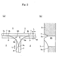
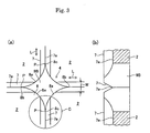
- Figs 2 and 3 show enlarged views of regions "B" and "C” in the vicinity of the crossing parts.
- a spacing 9A is defined by the adjacent two substrate regions 2 and the unused region 5.
- a corner part 8 faces a spacing 9A of the substrate region 2 and has a shape of an arc in a plane of the surface of the base plate 2.
- the center of curvature of each of the corner parts 8 is located inside of the corner part 8 (inside of the substrate region 2).
- the spacing 9A and dividing groove 7 contact each other at a crossing point "P".
- "L" represents the longitudinal direction of each dividing groove.
- a spacing 9B is defined by the adjoining four substrate regions 2.
- a corner part faces the spacing 9B of the substrate region 2 and has a shape of an arc in a plane of the surface of the base plate.
- the center of curvature of each of the corner parts 8 is located inside of the corner part 8 (inside of the substrate region 2).
- the spacing 9B and dividing groove 7 contact each other at a crossing point "P".
- "L" represents the longitudinal direction of each dividing groove.
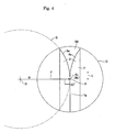
- Fig. 4 is an enlarged view showing a region in the vicinity of each contact point of the dividing groove and spacing. That is, "D" represents a virtual circle obtained by extending the outline of the corner part 8, “O” represents a center of curvature of the virtual circle “D”, and “R” represents a radius of curvature of the circle.
- the end part 8c (or 8b) of the corner part 8 is present on the cross point "P" of the spacing 9B (or 9A) and the center line 7a of the dividing groove 7. According to the present invention, the corner part 8 is tangent to the center line 7a (the center line in a plan view) of the dividing groove 7.
- the outline (along the virtual circle “D") of the corner part 8a is parallel with the longitudinal direction "L” of the center line 7a of the dividing groove 7. Further, provided that a radial line “F” is drawn from the center “O” of the virtual circle to the cross point "P", the radial line “F” is perpendicular to the center line 7a.
- the ceramic base plate when the ceramic base plate is broken along the dividing grooves, it is possible to prevent the breaking at positions different from the dividing grooves and unnecessary crack formation therein, so that the ceramic base plate can be assuredly broken and the yield can be improved.
- the angle of the groove should be small due tho the limitation of the production. This results in the groove with a very small width, so that a part of the opening of the groove tends to be closed during the sintering step to result in deterioration of the ease of breaking.
- the dividing groove is defined by at least a first inclined face and a second inclined face and the both faces make an angle of 25 to 90 ° , in a cross section perpendicular to the longitudinal direction "L" of the dividing groove. It is thereby possible to prevent the close of the groove opening during the sintering and the partly deterioration of the breaking characteristic, so that the deviation of the strength required for the breaking step can be reduced.
- the width "W" of the opening of the dividing groove is 0.1 to 0.5 mm at the surface of the ceramic base plate.
- at least a part of the corner part 8 has a shape of an arc in a plan view.
- the arc-shaped part of the corner part 8 is continuously formed with the end part 8b or 8c.
- the corner part has a shape of an arc in a range of 30 ° or more, more preferably 45 ° or more, with respect to the end part 8b or 8c. It is further preferred that 30 percent or more, more preferably 50 percent or more, of the length of the outline of the corner part 8 has a shape of an arc.
- Parts other than the arc-shaped part of the corner part may preferably be a straight line which is tangent to the arc-shaped part.
- the outer outline of the corner part 8 has a shape of an arc over the whole length.
- the radius of curvature "R" of the corner part 8 may preferably be 0.2 to 5.0 mm and more preferably be 0.5 to 2.5 mm, on the viewpoint of the present invention.
- the above described conditions are satisfied at the crossing parts 3 and 4 (A and B) where a plurality of the substrate regions cross.
- the base plate is not to be broken between the two substrate regions. Therefore, the above described conditions of the present invention may or may not be satisfied.
- the material forming the ceramic base plate is not particularly limited as far as it is used for an electronic device, and includes alumina, magnesia, silica, yttria, silicon nitride, boron nitride, titanium nitride, aluminum nitride, aluminum oxynitride, spinel, yttirum-aluminum garnet and the like.
- the present invention is particularly suitable to a dense alumina and particularly translucent alumina. It will be further described below about a ceramic substrate made of translucent alumina etc..
- Translucent ceramics particularly translucent alumina, may be used for a diffusion plate for a light emitting diode device, so that the operational life of the light emitting diode can be considerably improved.
- the thickness of the translucent ceramic substrate may preferably be 0.05 mm or more and 2 mm or less. In the case that the substrate is too thin, it may be susceptible to shock or the ratio of in-line transmittance becomes too high to result in shortage of light diffusion. In the case that the ceramic substrate is too thick, the total light transmittance becomes too low and the heat dissipation characteristic becomes low.
- the in-line transmittance of the translucent ceramic substrate in visible light range may preferably be 65 percent or less and more preferably be 10 percent or less, on the viewpoint of light diffusion.
- the total light transmittance of the translucent ceramic substrate may preferably be 90 percent or more on the viewpoint of efficiency of light emission.
- the crystal grain size of a ceramics forming the translucent ceramic substrate is not particularly limited and may preferably be 0.1 ⁇ m or larger and more preferably be 1 ⁇ m or larger, on the viewpoint of obtaining an appropriate translucent characteristic. Further, the crystal grain size of the ceramics may preferably be 100 ⁇ m or smaller and more preferably be 40 ⁇ m or smaller.
- the relative density of the ceramics forming the translucent ceramic substrate may preferably be 98 percent or higher and more preferably be 99 percent or higher, on the viewpoint of assuring the translucent characteristics. Light incident into the ceramics is scattered by pores in the ceramics so that the total light transmittance is considerably lowered.
- the molding method of the ceramic substrate is not particularly limited, and may be any method such as doctor blade, extrusion and gel cast molding methods. More preferably, the ceramic substrate is produced using gel cast molding. According to a preferred embodiment, slurry containing ceramic powder, a dispersant and a gelling agent is molded and then gelled to obtain a molded body, which is then sintered (Japanese Patent Publication No. 2001-335371A ). In the case of prior methods of forming grooves by pressing a cutter blade or press mold onto an unfired green sheet, micro cracks may be generated under the grooves and the breaking strength may be deviated. It is possible to avoid this problem by shaping the dividing grooves by protrusions formed on a mold using gel cast molding.
- a high purity alumina powder having a purity of 99.9 percent or more (more preferably 99.95 percent or more). It may be listed a high purity alumina powder supplied by Taimei Chemical Co. Ltd. as such high purity alumina powder.
- the above described aid may preferably be magnesium oxide and includes ZrO 2 , Y 2 O 3 , La 2 O 3 and Sc 2 O 3 .
- the average particle diameter of ceramic powdery raw material is not particularly limited, and may preferably be 0.5 ⁇ m or less and more preferably 0.4 ⁇ m or less, on the viewpoint of densification and improvement of translucent characteristic by sintering at low temperature. More preferably, the average particle diameter of the ceramic powdery raw material is 0.3 ⁇ m or less (Primary particle diameter). The lower limit of the average particle diameter is not particularly limited.
- the average particle diameter of the powdery raw material can be decided by direct observation of the powdery raw material by means of SEM (Scanning type electron microscope).
- the gel cast molding method includes the followings.
- a base plate 1 made of a translucent alumina ceramics was produced as follows. That is, 100 weight parts of alumina powder and 0.025 weight parts of magnesia as powdery raw materials, 30 weight parts of a polybasic acid ester as a dispersant, 4 weight parts of MDI resin as a gelling agent, 2 weight parts of "MALIALIM AKM0351" (trade name, supplied by NOF corporation) as a dispersant, and 0.2 weight parts of triethylamine as a catalyst were mixed to obtain slurry. The slurry was then casted at room temperature into a mold made of an aluminum alloy which has protrusions each having an inverted shape of a dividing groove, maintained at room temperature for 1 hour, and removed from the mold after the solidification.
- the dividing groove was made V-groove, the corner part of each substrate region was made an arc-shaped, and the dimensions were made as follows. Width "W" of opening of dividing groove 7: 0.3 mm Opening angle of dividing groove 7 (an angle of first and second inclined faces): 60 ° Depth of dividing groove 7: 0.26 mm Thickness of base plate 1: 1.0 mm Radius "R" of curvature of corner part 8: 0.5 mm Dimension of each substrate region 2: 25 mm ⁇ 25 mm
- the base plate was produced according to the same procedure as the Example 1.
- the base plate had a planar pattern shown in Fig. 1 .
- the dividing groove was made a V-groove, and its dimensions were same as those described in the Example 1.
- the corner parts of each substrate region did not have a shape of an arc and the planar shape of the spacing was made circular.
- the base plate was produced according to the same procedure as the Example 1.
- the base plate had a planar pattern shown in Fig. 1 .
- the dividing groove was made a V-groove, and its dimensions were same as those described in the Example 1.
- the corner parts opf each substrate region did not have a shape of an arc and had a shape described in Japanese patent Publication No. 1994-091628A .
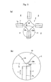
- a curved part 23 facing a spacing 21 was formed at the corner part of each substrate region.
- the end of the curved part 23 was in the vicinity of the end of the dividing groove 7, the end of the dividing groove 7 was not communicated with the spacing 21 with a non-spacing part 24 was provided therebetween.
- the tangential line "M" to an end 23b of the curved part 23 on the side of the dividing groove and the longitudinal direction "L" of the dividing groove 7 are made right angle, which was just the opposite to the case of the present invention (see Fig. 4 ).
- Example 1 Example 2
- Example 3 Comparative Example 1 Comparative Example 2 Width of opening at surface : mm 0.3mm 0.1mm 0.5mm 0.3mm 0.3mm Angle at bottom of groove : ° 6 0° 2 5° 9 0° 6 0° 6 0° Depth of groove : mm 0.26mm 0.26mm 0.26mm 0.26mm 0.26mm 0.26mm Shape of spacing Tangential Arc Tangential Arc Circle Curved Arc Force required for breaking : N/mm2 0.6 ⁇ 0.1 0.6 ⁇ 0.1 0.6 ⁇ 0.1 0.6 ⁇ 0.3 0.7 ⁇ 0.3 Shift from dividing groove 0/10 0/10 0/10 3/10 8/10
- a ceramic base plate is divided into a plurality of substrate regions 2 each having corner part 8.
- a dividing groove 7 is formed between the substrate regions 2 adjacent with each other.
- the corner part 8 of each of the substrate regions 2 faces a spacing 9B communicated with the dividing groove 7.
- At least a part of the corner part 8 is arc-shaped.
- the arc-shaped part of the corner part is tangent to a center line 7a of the dividing groove 7 at a cross point "P" of the spacing 9B with the dividing groove 7.
- the ceramic base plate is broken along the dividing groove 7 to produce ceramic substrates.
Landscapes
- Engineering & Computer Science (AREA)
- Mechanical Engineering (AREA)
- Manufacturing & Machinery (AREA)
- Microelectronics & Electronic Packaging (AREA)
- Structure Of Printed Boards (AREA)
Abstract
A ceramic base plate is divided into a plurality of substrate regions 2 each having corner part 8. A dividing groove 7 is formed between the substrate regions 2 adjacent with each other. The corner part 8 of each of the substrate regions 2 faces a spacing 9B communicated with the dividing groove 7. At least a part of the corner part 8 is arc-shaped. The arc-shaped part of the corner part is tangent to a center line 7a of the dividing groove 7 at a cross point "P" of the spacing 9B with the dividing groove 7. The ceramic base plate is broken along the dividing groove 7 to produce ceramic substrates.
Description
- The present invention relates to a method of producing ceramic substrates by breaking a ceramic base plate.
- Alumina ceramics has been widely used for a substrate for electronic devices owing to its characteristics such as electrical insulation and chemical stability. In producing such substrates, many substrate regions are provided in a single base plate of a large area, for facilitating its handling and for improving subsequent production efficiency of electronic devices such as printing of wiring patterns and mounting of semiconductor devices. In producing such substrates, breaking grooves (dividing grooves) are formed on a surface of the base plate for facilitating the breaking into respective pieces. Such dividing grooves may be formed by producing a ceramic unfired green sheet shaped by doctor blade or the like, forming cuttings on the surface of the green sheets by pressing a cutter blade or press metal mold thereon, and then firing the green sheet (Japanese Patent Nos.
3,330,104B 3,876,259B - Here, for example as shown in
Fig. 1 , spacings are formed at crossing parts A and B of each of the pieces (each of the ceramic substrate regions) 2. Various techniques have been proposed about the shape of the spacing (Japanese Patent Publication No.1982-197,889A 1990-133,987A 1982-181,060A 1983-049,464A 1985-066,061A 2008-060,096A 1994-091,628A - Besides, it is descried, in Japanese Patent Publication No.
2001-335,371A - According to the prior arts, in breaking a base plate along dividing grooves, the base plate may be broken along a line different from the dividing grooves to result in a reduction of yield. It is possible to assist the breaking along the dividing groove by making the groove deeper toward the bottom face of the base plate. In this case, however, the mechanical strength of the base plate would be considerably lowered so that the base plate may be easily broken during handling for printing etc.. It is thus impossible to make the dividing groove deeper than a predetermined depth.
- An object of the present invention is to produce ceramic substrates by breaking a ceramic base plate along dividing grooves so that it can be broken along the dividing grooves.
- The present invention provides a method of producing a plurality of ceramic substrates by breaking a ceramic base plate,
wherein the ceramic base plate comprises a plurality of substrate regions divided with each other, the substrate region comprising a corner part;
wherein a dividing groove is formed between the substrate regions adjacent with each other;
wherein the corner part of each of the substrate regions faces a spacing communicated with the dividing groove;
wherein at least a part of the corner part has a shape of an arc; and
wherein the arc-shaped part of the corner part is tangent to a center line of the dividing groove at a cross point of the spacing with the dividing groove;
the method comprising the step of producing the ceramic substrates by breaking the ceramic base plate along the dividing groove. - According to the present invention, in breaking the base plate along the dividing grooves, it is possible to prevent the fracture of the base plate along a line different from the dividing grooves.
- These and other objects, features and advantages of the invention will be appreciated upon reading the following description of the invention when taken in conjunction with the attached drawings, with the understanding that some modifications, variations and changes of the same could be made by the skilled person in the art.
-
-
Fig. 1 is a plan view schematically showing a ceramic base plate 1. -
Fig. 2 is a plan view showing an enlarged view of part "A" of the base plate 1 ofFig. 1 , andFig. 2 (b) is a cross sectional view of the "A" part ofFig. 2 (a) . -
Fig. 3 is a plan view showing an enlarged view of part "B" of the base plate 1 ofFig. 1 , andFig. 3(b) is a cross sectional view of the "B" part ofFig. 2 (a) . -
Fig. 4 is a diagram showing positional relationship of a central line of a dividing groove and a corner part of a substrate region, according to the present invention. -
Fig. 5 (a) is a plan view showing shapes and positional relationship of a spacing and a dividing groove according to a comparative example, andFig. 5 (b) is an enlarged view showing a region "E" in the vicinity of an end part of the dividing groove and an end part of the spacing. - As shown in
Fig. 1 , a ceramic base plate 1 is divided into a plurality ofsubstrate regions 2, and a dividing groove is formed between theadjacent substrate regions 2. At crossingparts substrate regions 2, spacings are formed, respectively, so that the spacings are communicated with the dividing grooves. Areference numeral 5 represents a non-used region which is not used in a product. InFig. 1 , corner parts of the two substrate regions cross at thecrossing part 3, and corner parts of the four substrate regions cross at thecrossing part 4. -
Figs 2 and3 show enlarged views of regions "B" and "C" in the vicinity of the crossing parts. InFig. 2 , aspacing 9A is defined by the adjacent twosubstrate regions 2 and theunused region 5. Acorner part 8 faces a spacing 9A of thesubstrate region 2 and has a shape of an arc in a plane of the surface of thebase plate 2. The center of curvature of each of thecorner parts 8 is located inside of the corner part 8 (inside of the substrate region 2). The spacing 9A and dividinggroove 7 contact each other at a crossing point "P". "L" represents the longitudinal direction of each dividing groove. - Further, as shown in
Fig. 3 , aspacing 9B is defined by the adjoining foursubstrate regions 2. A corner part faces the spacing 9B of thesubstrate region 2 and has a shape of an arc in a plane of the surface of the base plate. The center of curvature of each of thecorner parts 8 is located inside of the corner part 8 (inside of the substrate region 2). The spacing 9B and dividinggroove 7 contact each other at a crossing point "P". "L" represents the longitudinal direction of each dividing groove. -
Fig. 4 is an enlarged view showing a region in the vicinity of each contact point of the dividing groove and spacing. That is, "D" represents a virtual circle obtained by extending the outline of thecorner part 8, "O" represents a center of curvature of the virtual circle "D", and "R" represents a radius of curvature of the circle. Theend part 8c (or 8b) of thecorner part 8 is present on the cross point "P" of the spacing 9B (or 9A) and thecenter line 7a of the dividinggroove 7. According to the present invention, thecorner part 8 is tangent to thecenter line 7a (the center line in a plan view) of the dividinggroove 7. In other words, at the cross point "P" (orend part corner part 8a is parallel with the longitudinal direction "L" of thecenter line 7a of thedividing groove 7. Further, provided that a radial line "F" is drawn from the center "O" of the virtual circle to the cross point "P", the radial line "F" is perpendicular to thecenter line 7a. - According to the present invention, when the ceramic base plate is broken along the dividing grooves, it is possible to prevent the breaking at positions different from the dividing grooves and unnecessary crack formation therein, so that the ceramic base plate can be assuredly broken and the yield can be improved.
- In the case that the dividing groove is formed by a cutter blade or press blade, the angle of the groove should be small due tho the limitation of the production. This results in the groove with a very small width, so that a part of the opening of the groove tends to be closed during the sintering step to result in deterioration of the ease of breaking. Thus, according to a preferred embodiment, the dividing groove is defined by at least a first inclined face and a second inclined face and the both faces make an angle of 25 to 90 ° , in a cross section perpendicular to the longitudinal direction "L" of the dividing groove. It is thereby possible to prevent the close of the groove opening during the sintering and the partly deterioration of the breaking characteristic, so that the deviation of the strength required for the breaking step can be reduced.
- Further, according to a preferred embodiment, the width "W" of the opening of the dividing groove is 0.1 to 0.5 mm at the surface of the ceramic base plate.
According to the present invention, at least a part of thecorner part 8 has a shape of an arc in a plan view. Here, it is preferred that the arc-shaped part of thecorner part 8 is continuously formed with theend part end part corner part 8 has a shape of an arc. Parts other than the arc-shaped part of the corner part may preferably be a straight line which is tangent to the arc-shaped part. It is further preferred that the outer outline of thecorner part 8 has a shape of an arc over the whole length. - The radius of curvature "R" of the corner part 8 (radius "R" of the virtual circle "D") may preferably be 0.2 to 5.0 mm and more preferably be 0.5 to 2.5 mm, on the viewpoint of the present invention.
- Further, according to the present invention, it is required that the above described conditions are satisfied at the
crossing parts 3 and 4 (A and B) where a plurality of the substrate regions cross. However, at a crossing part where onesubstrate region 2 and theunused region 5 contact with each other, the base plate is not to be broken between the two substrate regions. Therefore, the above described conditions of the present invention may or may not be satisfied. - The material forming the ceramic base plate is not particularly limited as far as it is used for an electronic device, and includes alumina, magnesia, silica, yttria, silicon nitride, boron nitride, titanium nitride, aluminum nitride, aluminum oxynitride, spinel, yttirum-aluminum garnet and the like.
- The present invention is particularly suitable to a dense alumina and particularly translucent alumina. It will be further described below about a ceramic substrate made of translucent alumina etc..
- Translucent ceramics, particularly translucent alumina, may be used for a diffusion plate for a light emitting diode device, so that the operational life of the light emitting diode can be considerably improved.
- The thickness of the translucent ceramic substrate may preferably be 0.05 mm or more and 2 mm or less. In the case that the substrate is too thin, it may be susceptible to shock or the ratio of in-line transmittance becomes too high to result in shortage of light diffusion. In the case that the ceramic substrate is too thick, the total light transmittance becomes too low and the heat dissipation characteristic becomes low.
- The in-line transmittance of the translucent ceramic substrate in visible light range may preferably be 65 percent or less and more preferably be 10 percent or less, on the viewpoint of light diffusion. The total light transmittance of the translucent ceramic substrate may preferably be 90 percent or more on the viewpoint of efficiency of light emission.
- The crystal grain size of a ceramics forming the translucent ceramic substrate is not particularly limited and may preferably be 0.1 µm or larger and more preferably be 1 µm or larger, on the viewpoint of obtaining an appropriate translucent characteristic. Further, the crystal grain size of the ceramics may preferably be 100 µm or smaller and more preferably be 40 µm or smaller.
- Further, the relative density of the ceramics forming the translucent ceramic substrate may preferably be 98 percent or higher and more preferably be 99 percent or higher, on the viewpoint of assuring the translucent characteristics. Light incident into the ceramics is scattered by pores in the ceramics so that the total light transmittance is considerably lowered.
- The molding method of the ceramic substrate is not particularly limited, and may be any method such as doctor blade, extrusion and gel cast molding methods. More preferably, the ceramic substrate is produced using gel cast molding. According to a preferred embodiment, slurry containing ceramic powder, a dispersant and a gelling agent is molded and then gelled to obtain a molded body, which is then sintered (Japanese Patent Publication No.
2001-335371A
In the case of prior methods of forming grooves by pressing a cutter blade or press mold onto an unfired green sheet, micro cracks may be generated under the grooves and the breaking strength may be deviated. It is possible to avoid this problem by shaping the dividing grooves by protrusions formed on a mold using gel cast molding. - More preferably, it is used raw material obtained by adding 150 to 1000 ppm of an aid to a high purity alumina powder having a purity of 99.9 percent or more (more preferably 99.95 percent or more). It may be listed a high purity alumina powder supplied by Taimei Chemical Co. Ltd. as such high purity alumina powder.
The above described aid may preferably be magnesium oxide and includes ZrO2, Y2O3, La2O3 and Sc2O3. - The average particle diameter of ceramic powdery raw material is not particularly limited, and may preferably be 0.5 µm or less and more preferably 0.4 µm or less, on the viewpoint of densification and improvement of translucent characteristic by sintering at low temperature. More preferably, the average particle diameter of the ceramic powdery raw material is 0.3 µm or less (Primary particle diameter). The lower limit of the average particle diameter is not particularly limited. The average particle diameter of the powdery raw material can be decided by direct observation of the powdery raw material by means of SEM (Scanning type electron microscope).
Besides, the average particle diameter referred to herein means an average value at n = 500 of values of (maximum major axis length + minimum minor axis length)/ 2 of primary particles excluding secondary aggregated particles, in SEM photographs (in optional two areas at a magnitude of × 30000). - The gel cast molding method includes the followings.
- (1) A prepolymer functioning as a gelling agent such as polyvinyl alcohol, epoxy resin, phenolic resin or the like is dispersed in a dispersing medium with inorganic powder and a dispersant to produce slurry, which is then molded and gelled and solidified by crosslinking in three dimensional manner using a crosslinking agent.
- (2) An organic dispersant having a reactive functional group is chemically bonded with a gelling agent to solidify the slurry.
- A base plate 1 made of a translucent alumina ceramics was produced as follows. That is, 100 weight parts of alumina powder and 0.025 weight parts of magnesia as powdery raw materials, 30 weight parts of a polybasic acid ester as a dispersant, 4 weight parts of MDI resin as a gelling agent, 2 weight parts of "MALIALIM AKM0351" (trade name, supplied by NOF corporation) as a dispersant, and 0.2 weight parts of triethylamine as a catalyst were mixed to obtain slurry. The slurry was then casted at room temperature into a mold made of an aluminum alloy which has protrusions each having an inverted shape of a dividing groove, maintained at room temperature for 1 hour, and removed from the mold after the solidification. Further, the molded body was maintained at room temperature for 2 hours and then at 90 °C for 2 hours to obtain a dried molded body of powder having a shape of a base plate. It was then calcined at 1200 °C in air to obtain a calcined body. The calcined body was then sintered at 1800 °C in an atmosphere of hydrogen : nitrogen = 3:1 so that the sintered body was densified and made translucent. The shape and pattern of the dividing groove or the like were adjusted by changing the shape and pattern of the protrusions formed on the mold.
- However, as shown in
Figs 1 to 4 , the dividing groove was made V-groove, the corner part of each substrate region was made an arc-shaped, and the dimensions were made as follows.
Width "W" of opening of dividing groove 7: 0.3 mm
Opening angle of dividing groove 7 (an angle of first and second inclined faces): 60 °
Depth of dividing groove 7: 0.26 mm
Thickness of base plate 1: 1.0 mm
Radius "R" of curvature of corner part 8: 0.5 mm
Dimension of each substrate region 2: 25 mm × 25 mm - Ten samples of the base plate were thus produced and broken along the respective dividing grooves. As a result, the deviation of a force required for the breaking was proved to be 0.6 ± 0.1 N/mm. Further, the broken line was not out of the dividing grooves in all of the ten samples.
- The base plate was produced according to the same procedure as the Example 1. The base plate had a planar pattern shown in
Fig. 1 . Further, the dividing groove was made a V-groove, and its dimensions were same as those described in the Example 1. However, the corner parts of each substrate region did not have a shape of an arc and the planar shape of the spacing was made circular. - Ten samples of the base plate were broken along the dividing grooves, respectively. As a result, the deviation of a force required for the breaking was proved to be 0.6 ± 0.3 N/mm. Further, the broken line was out of the dividing grooves in three of the ten samples.
- The base plate was produced according to the same procedure as the Example 1. The base plate had a planar pattern shown in
Fig. 1 . Further, the dividing groove was made a V-groove, and its dimensions were same as those described in the Example 1. However, the corner parts opf each substrate region did not have a shape of an arc and had a shape described in Japanese patent Publication No.1994-091628A - That is, as shown in
Figs. 5 (a) and (b) , acurved part 23 facing aspacing 21 was formed at the corner part of each substrate region. Although the end of thecurved part 23 was in the vicinity of the end of the dividinggroove 7, the end of the dividinggroove 7 was not communicated with the spacing 21 with anon-spacing part 24 was provided therebetween. The tangential line "M" to anend 23b of thecurved part 23 on the side of the dividing groove and the longitudinal direction "L" of the dividinggroove 7 are made right angle, which was just the opposite to the case of the present invention (seeFig. 4 ). - Ten samples of the base plate were broken along the dividing grooves, respectively. As a result, the deviation of a force required for the breaking was proved to be 0.7 ± 0.3 N/mm. Further, the
non-spacing part 24 between the dividinggroove 7 andspacing 21 were broken in indeterminate forms to leave needle-like protrusions in eight of the ten samples. - Test was performed according to the same procedure as the Example 1 except that the width of the opening and angle of the bottom of the groove were changed as shown in Table 1, and the results were shown in Table 1.
Table 1 Example 1 Example 2 Example 3 Comparative Example 1 Comparative Example 2 Width of opening at surface : mm 0.3mm 0.1mm 0.5mm 0.3mm 0.3mm Angle at bottom of groove : ° 6 0° 2 5° 9 0° 6 0° 6 0° Depth of groove : mm 0.26mm 0.26mm 0.26mm 0.26mm 0.26mm Shape of spacing Tangential Arc Tangential Arc Tangential Arc Circle Curved Arc Force required for breaking : N/mm2 0.6±0.1 0.6±0.1 0.6±0.1 0.6±0.3 0.7±0.3 Shift from dividing groove 0/10 0/10 0/10 3/10 8/10 - The present invention has been explained referring to the preferred embodiments , however , the present invention is not limited to the illustrated embodiments which are given by way of examples only , and may be carried out in various modes without departing from the scope of the invention.
- A ceramic base plate is divided into a plurality of
substrate regions 2 each havingcorner part 8. A dividinggroove 7 is formed between thesubstrate regions 2 adjacent with each other. Thecorner part 8 of each of thesubstrate regions 2 faces aspacing 9B communicated with the dividinggroove 7. At least a part of thecorner part 8 is arc-shaped. The arc-shaped part of the corner part is tangent to acenter line 7a of the dividinggroove 7 at a cross point "P" of thespacing 9B with the dividinggroove 7. The ceramic base plate is broken along the dividinggroove 7 to produce ceramic substrates.
Claims (5)
- A method of producing a plurality of ceramic substrates by breaking a ceramic base plate,
wherein said ceramic base plate comprises a plurality of substrate regions divided with each other, said substrate region comprising a corner part;
wherein a dividing groove is formed between said substrate regions adjacent with each other;
wherein said corner part of each of said substrate regions faces a spacing communicated with said dividing groove;
wherein at least a part of said corner part is arc-shaped; and
wherein said arc-shaped part of said corner part is tangent to a center line of said dividing groove at a cross point of said spacing with said dividing groove;
the method comprising the step of producing said ceramic substrates by breaking said ceramic base plate along said dividing groove. - The method of claim 1, wherein said dividing groove comprises a first inclined face and an opposing second inclined face viewed in a cross section perpendicular to the longitudinal direction of said dividing groove, and wherein said first and second inclined faces make an angle of 25 to 90 °.
- The method of claim 1 or 2, wherein said dividing groove has an open width of 0.1 to 0.5 mm at a surface of said ceramic base plate.
- The method of any one of claims 1 to 3, wherein said ceramic base plate comprises a translucent alumina ceramics.
- The method of any one of claims 1 to 4, wherein said ceramic base plate is produced by gel casting.
Applications Claiming Priority (1)
| Application Number | Priority Date | Filing Date | Title |
|---|---|---|---|
| JP2011092651A JP2012227306A (en) | 2011-04-19 | 2011-04-19 | Manufacturing method of ceramic substrate |
Publications (1)
| Publication Number | Publication Date |
|---|---|
| EP2514576A1 true EP2514576A1 (en) | 2012-10-24 |
Family
ID=45976819
Family Applications (1)
| Application Number | Title | Priority Date | Filing Date |
|---|---|---|---|
| EP20120164579 Withdrawn EP2514576A1 (en) | 2011-04-19 | 2012-04-18 | A method of producing ceramic substrates |
Country Status (4)
| Country | Link |
|---|---|
| US (1) | US20120267412A1 (en) |
| EP (1) | EP2514576A1 (en) |
| JP (1) | JP2012227306A (en) |
| CN (1) | CN102752960A (en) |
Cited By (2)
| Publication number | Priority date | Publication date | Assignee | Title |
|---|---|---|---|---|
| EP2953157A4 (en) * | 2014-01-06 | 2016-02-24 | Ngk Insulators Ltd | HANDLING SUBSTRATE AND COMPOSITE WAFER FOR SEMICONDUCTOR DEVICE |
| EP3448133A4 (en) * | 2016-04-22 | 2019-12-18 | Kyocera Corporation | MULTI-ELEMENT WIRING BOARD, MANUFACTURING METHOD THEREOF, AND WIRING BOARD |
Families Citing this family (3)
| Publication number | Priority date | Publication date | Assignee | Title |
|---|---|---|---|---|
| JP6249348B2 (en) * | 2013-11-22 | 2017-12-20 | 東芝ライテック株式会社 | Light emitting device |
| US9287106B1 (en) | 2014-11-10 | 2016-03-15 | Corning Incorporated | Translucent alumina filaments and tape cast methods for making |
| EP3361839A1 (en) * | 2017-02-14 | 2018-08-15 | Infineon Technologies AG | Multiple substrate and method for its fabrication |
Citations (12)
| Publication number | Priority date | Publication date | Assignee | Title |
|---|---|---|---|---|
| JPS57181060A (en) | 1981-04-24 | 1982-11-08 | Beecham Group Ltd | Imidazole derivatives, manufacture and medicinal composition containing them |
| JPS57197889A (en) | 1981-05-29 | 1982-12-04 | Tokyo Shibaura Electric Co | Printed circuit board |
| JPS5849464A (en) | 1981-07-14 | 1983-03-23 | ラインハルト・テヒニク・ゲゼルシヤフト・ミツト・ベシユレンクテル・ハフトウング・ウント・コンバニ− | Applicator gun |
| JPS6066061A (en) | 1983-09-21 | 1985-04-16 | Matsushita Electric Ind Co Ltd | solar heat collector |
| JPH02133987A (en) | 1988-11-15 | 1990-05-23 | Taiyo Yuden Co Ltd | Method and substrate for producing hybrid integrated circuit |
| JPH0691628A (en) | 1991-11-19 | 1994-04-05 | Ishizuka Glass Co Ltd | Ceramic substrate manufacturing method |
| US6033289A (en) * | 1998-08-25 | 2000-03-07 | International Business Machines Corporation | Detailing and cleaning apparatus for green ceramic dry dicing process |
| JP2001335371A (en) | 2000-03-22 | 2001-12-04 | Ngk Insulators Ltd | Manufacturing method of powder compact |
| JP3330104B2 (en) | 1999-07-29 | 2002-09-30 | 京セラ株式会社 | Manufacturing method of multi-cavity ceramic wiring board |
| JP3876259B2 (en) | 2004-08-04 | 2007-01-31 | 日本特殊陶業株式会社 | Manufacturing method of ceramic substrate |
| JP2008060096A (en) | 2006-08-29 | 2008-03-13 | Ngk Spark Plug Co Ltd | Multi-piece wiring board and manufacturing method thereof |
| WO2011152085A1 (en) * | 2010-06-04 | 2011-12-08 | 株式会社 村田製作所 | Method for producing integrated substrate |
Family Cites Families (5)
| Publication number | Priority date | Publication date | Assignee | Title |
|---|---|---|---|---|
| JP2000315841A (en) * | 1999-04-28 | 2000-11-14 | Kyocera Corp | Ceramic substrate for electronic components |
| JP2006210655A (en) * | 2005-01-28 | 2006-08-10 | Kyocera Corp | Multiple wiring board |
| JP4969119B2 (en) * | 2006-03-20 | 2012-07-04 | 日本碍子株式会社 | Light emitting diode device |
| DE602007011286D1 (en) * | 2006-08-07 | 2011-01-27 | Murata Manufacturing Co | METHOD FOR PRODUCING A CERAMIC, MULTILAYER SUBSTRATE |
| JP2009099681A (en) * | 2007-10-15 | 2009-05-07 | Shinko Electric Ind Co Ltd | Substrate separation method |
-
2011
- 2011-04-19 JP JP2011092651A patent/JP2012227306A/en active Pending
-
2012
- 2012-04-13 US US13/446,357 patent/US20120267412A1/en not_active Abandoned
- 2012-04-17 CN CN2012101132649A patent/CN102752960A/en active Pending
- 2012-04-18 EP EP20120164579 patent/EP2514576A1/en not_active Withdrawn
Patent Citations (12)
| Publication number | Priority date | Publication date | Assignee | Title |
|---|---|---|---|---|
| JPS57181060A (en) | 1981-04-24 | 1982-11-08 | Beecham Group Ltd | Imidazole derivatives, manufacture and medicinal composition containing them |
| JPS57197889A (en) | 1981-05-29 | 1982-12-04 | Tokyo Shibaura Electric Co | Printed circuit board |
| JPS5849464A (en) | 1981-07-14 | 1983-03-23 | ラインハルト・テヒニク・ゲゼルシヤフト・ミツト・ベシユレンクテル・ハフトウング・ウント・コンバニ− | Applicator gun |
| JPS6066061A (en) | 1983-09-21 | 1985-04-16 | Matsushita Electric Ind Co Ltd | solar heat collector |
| JPH02133987A (en) | 1988-11-15 | 1990-05-23 | Taiyo Yuden Co Ltd | Method and substrate for producing hybrid integrated circuit |
| JPH0691628A (en) | 1991-11-19 | 1994-04-05 | Ishizuka Glass Co Ltd | Ceramic substrate manufacturing method |
| US6033289A (en) * | 1998-08-25 | 2000-03-07 | International Business Machines Corporation | Detailing and cleaning apparatus for green ceramic dry dicing process |
| JP3330104B2 (en) | 1999-07-29 | 2002-09-30 | 京セラ株式会社 | Manufacturing method of multi-cavity ceramic wiring board |
| JP2001335371A (en) | 2000-03-22 | 2001-12-04 | Ngk Insulators Ltd | Manufacturing method of powder compact |
| JP3876259B2 (en) | 2004-08-04 | 2007-01-31 | 日本特殊陶業株式会社 | Manufacturing method of ceramic substrate |
| JP2008060096A (en) | 2006-08-29 | 2008-03-13 | Ngk Spark Plug Co Ltd | Multi-piece wiring board and manufacturing method thereof |
| WO2011152085A1 (en) * | 2010-06-04 | 2011-12-08 | 株式会社 村田製作所 | Method for producing integrated substrate |
Cited By (3)
| Publication number | Priority date | Publication date | Assignee | Title |
|---|---|---|---|---|
| EP2953157A4 (en) * | 2014-01-06 | 2016-02-24 | Ngk Insulators Ltd | HANDLING SUBSTRATE AND COMPOSITE WAFER FOR SEMICONDUCTOR DEVICE |
| US9390955B2 (en) | 2014-01-06 | 2016-07-12 | Ngk Insulators, Ltd. | Handle substrate and composite wafer for semiconductor device |
| EP3448133A4 (en) * | 2016-04-22 | 2019-12-18 | Kyocera Corporation | MULTI-ELEMENT WIRING BOARD, MANUFACTURING METHOD THEREOF, AND WIRING BOARD |
Also Published As
| Publication number | Publication date |
|---|---|
| US20120267412A1 (en) | 2012-10-25 |
| JP2012227306A (en) | 2012-11-15 |
| CN102752960A (en) | 2012-10-24 |
Similar Documents
| Publication | Publication Date | Title |
|---|---|---|
| US20120267412A1 (en) | Method of producing ceramic substrates | |
| US7008220B2 (en) | Ceramic setter plate and manufacturing method thereof | |
| US9538653B2 (en) | Insulating substrates including through holes | |
| JP2009252971A (en) | Metal-ceramics bonding substrate, manufacturing method therefor, and metal-ceramics bonding body | |
| EP1726419B1 (en) | Process for producing a ceramic sheet | |
| WO2012133525A1 (en) | Member for firing, container for firing using same, and method for producing positive electrode material | |
| KR102890629B1 (en) | silicon nitride substrate | |
| JP5829695B2 (en) | Heat sink and electronic component device including the heat sink | |
| EP3670474B1 (en) | Ceramic sheet and method for manufacturing the same | |
| KR101271563B1 (en) | Cutting sintered ceramic sheet and method for producing the same | |
| JP2002114579A (en) | Firing setter | |
| JP3429126B2 (en) | Method of manufacturing ceramic member having fine through holes | |
| US20060263552A1 (en) | Tray for heat treatment and method of manufacturing ceramic product using the tray | |
| JP4674397B2 (en) | Manufacturing method of ceramic body | |
| GB2315458A (en) | Manufacturing a ceramic member | |
| CN113454414A (en) | Ceramic structure | |
| JP4625654B2 (en) | Ceramic cover for setter | |
| JP3602300B2 (en) | Manufacturing method of ceramic member | |
| JP2013252678A (en) | Ceramic substrate manufacturing method and ceramic base material | |
| JP2005154790A (en) | Method of producing ceramic board, and ceramic board | |
| CN114207892B (en) | Electrolyte sheet for solid oxide fuel cell, method for producing electrolyte sheet for solid oxide fuel cell, and single cell for solid oxide fuel cell | |
| JP2003019711A (en) | Manufacturing method of ceramic substrate | |
| JP7566051B2 (en) | Wiring Board | |
| JPH10235914A (en) | Glaze substrate for thermal head and method of manufacturing the same | |
| JP2018203548A (en) | Zygote |
Legal Events
| Date | Code | Title | Description |
|---|---|---|---|
| PUAI | Public reference made under article 153(3) epc to a published international application that has entered the european phase |
Free format text: ORIGINAL CODE: 0009012 |
|
| AK | Designated contracting states |
Kind code of ref document: A1 Designated state(s): AL AT BE BG CH CY CZ DE DK EE ES FI FR GB GR HR HU IE IS IT LI LT LU LV MC MK MT NL NO PL PT RO RS SE SI SK SM TR |
|
| AX | Request for extension of the european patent |
Extension state: BA ME |
|
| 17P | Request for examination filed |
Effective date: 20130418 |
|
| STAA | Information on the status of an ep patent application or granted ep patent |
Free format text: STATUS: THE APPLICATION HAS BEEN WITHDRAWN |
|
| 18W | Application withdrawn |
Effective date: 20150105 |