EP2509103A1 - Apparatus and method for thermal connection - Google Patents
Apparatus and method for thermal connection Download PDFInfo
- Publication number
- EP2509103A1 EP2509103A1 EP11160939A EP11160939A EP2509103A1 EP 2509103 A1 EP2509103 A1 EP 2509103A1 EP 11160939 A EP11160939 A EP 11160939A EP 11160939 A EP11160939 A EP 11160939A EP 2509103 A1 EP2509103 A1 EP 2509103A1
- Authority
- EP
- European Patent Office
- Prior art keywords
- semiconductor
- base plate
- protrusions
- heat load
- contact
- Prior art date
- Legal status (The legal status is an assumption and is not a legal conclusion. Google has not performed a legal analysis and makes no representation as to the accuracy of the status listed.)
- Withdrawn
Links
Images

Classifications
-
- H—ELECTRICITY
- H10—SEMICONDUCTOR DEVICES; ELECTRIC SOLID-STATE DEVICES NOT OTHERWISE PROVIDED FOR
- H10W—GENERIC PACKAGES, INTERCONNECTIONS, CONNECTORS OR OTHER CONSTRUCTIONAL DETAILS OF DEVICES COVERED BY CLASS H10
- H10W40/00—Arrangements for thermal protection or thermal control
- H10W40/10—Arrangements for heating
-
- H—ELECTRICITY
- H10—SEMICONDUCTOR DEVICES; ELECTRIC SOLID-STATE DEVICES NOT OTHERWISE PROVIDED FOR
- H10W—GENERIC PACKAGES, INTERCONNECTIONS, CONNECTORS OR OTHER CONSTRUCTIONAL DETAILS OF DEVICES COVERED BY CLASS H10
- H10W40/00—Arrangements for thermal protection or thermal control
- H10W40/01—Manufacture or treatment
- H10W40/03—Manufacture or treatment of arrangements for cooling
- H10W40/037—Assembling together parts thereof
Definitions
- This invention relates to a solution for ensuring sufficient cooling of a semiconductor.
- the amount of heat generated by a semiconductor is often of such an extent that the heat needs to be transferred away from the semiconductor and the base plate to which the semiconductor is arranged in order to avoid malfunctions caused by a rise in the temperature.
- thermal grease between surfaces of parts to ensure that sufficient heat transfer is obtained over the interface between these parts.
- thermal grease contains chemical compounds which may have harmful effects on humans and therefore require care during handling.
- the thermal conductivity of the grease may also decrease during the life of the apparatus.
- the assembly of the apparatus is slower due to the need to apply thermal grease to the correct contact surfaces.
- An object of the present invention is to solve the above-mentioned drawback and to provide a novel solution for removing a heat load from a semiconductor in an apparatus. This object is achieved with the apparatus of independent claim 1 and the method of independent claim 8.
- Figure 1 illustrates a first embodiment of an apparatus
- Figure 2 illustrates a second embodiment of an apparatus
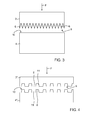
- Figure 3 illustrates a first embodiment of obtaining a thermal connection
- Figure 4 illustrates a second embodiment of obtaining a thermal connection.
- Figure 1 illustrates a first embodiment of an apparatus 1.
- the apparatus 1 includes at least one semiconductor 2, though in the illustrated example four semiconductors 2 are shown by way of example.
- the illustrated apparatus may be a part of a motor drive, such as a frequency converter.
- the semiconductor 2 is attached to a base plate 3 which may be used for electrically connecting the semiconductor 2 to external devices.
- the semiconductor device 2 generates a heat load that needs to be dissipated in order to avoid that the temperature of the semiconductor rises to an extent where malfunctions may occur.
- a surface of the base plate 3 is therefore in contact with a surface of an element 4 in order to forward the heat load generated by the semiconductor to the element 4.
- the element 4 consist of a cooling element with fins 5.
- the element 5 therefore transfers the heat load from the semiconductor 2 into the surrounding air via the fins 5.
- the cooling element may include a channel for a cooling fluid, for instance, in which case the heat load from the semiconductor 2 is transferred to the fluid by the cooling element.
- circulation of the fluid may ensure that the hot fluid is transferred away from the cooling element in order to replace the hot fluid with fluid that has cooled down in an external device, for instance.
- At least one of these surfaces is provided with a plurality of protrusions 6 that at least partly penetrate into the other one of said surfaces. This is illustrated in more detail in Figures 3 and 4 .
- Figure 2 illustrates a second embodiment of an apparatus 1'.
- the embodiment of Figure 2 is very similar to the one explained in connection with Figure 1 . Therefore, the embodiment of Figure 2 will be explained in the following mainly by pointing out the differences between these embodiments.
- the semiconductor 2 or semiconductors are encapsulated into a semiconductor module, and the base plate 6 forms a part of this semiconductor module.
- a second plate 7, which may be similar to the base plate 6, is arranged on top of the semiconductor 2 and attached to the semiconductor 2.
- a suitable material 8 such as a plastic material
- the plate 7 has an upper surface contacting an element 4', which may be a conductor rail electrically connecting the semiconductor 2 to an external device.
- heat generated by the semiconductor 2 is transferred away from the semiconductor module via the element 4'.
- at least one of these surfaces is provided with a plurality of protrusions 6 that at least partly penetrate into the other one of said surfaces. This is illustrated in more detail in Figures 3 and 4 .
- Figure 3 illustrates a first embodiment of obtaining a thermal connection.
- a solution may be used between the base plate 3 and the element 4 or between the plate 7 and the element 4', as illustrated in Figures 1 and 2 .
- the following explanation relates specifically to the interface between the base plate 3 and the element 4.
- the surface 9 of the base plate 3 is provided with sharp protrusions 6.
- the protrusions 6 may consist of areas located between V-shaped elongated grooves that have been provided in substantially the entire surface area of the surface 9.
- the protrusions 6 may consist of a plurality of conical protrusions provided in substantially the entire surface area of the surface 9.
- the surface 10 of the element 4 is smooth.
- a force F is utilized to press the base plate 3 towards the element 4 until the sharp protrusions 6 at least partly penetrate into the surface 10 of the element 4.
- the base plate 3 and element 4 may be attached to each other with screws, for instance. Due to the protrusions 6 penetrating at least partly into the surface 10 of the element 4, excellent heat conductivity is achieved.
- the protrusions are preferably manufactured of a material which is harder than the opposite surface.
- a material which is harder than the opposite surface is preferably utilized.
- MMC Metal Matrix Composite
- the base plate 3 and element 4 may be manufactured entirely of such materials, or alternatively both or only one of the surfaces is covered by a layer of a suitable material.
- Figure 4 illustrates a second embodiment of obtaining a thermal connection.
- the embodiment of Figure 4 is very similar to the one explained in connection with Figure 3 .
- both surfaces 9 and 10 of the base plate 3" and the element 4" are provided with protrusions 6.
- the surfaces 9 and 10 are also provided with recesses 11 for receiving protrusions of the opposite surface. Therefore, the recesses need not be sharp and the force F needed to ensure that the protrusions 6 penetrate into the opposite surface (recesses 11) may be much smaller than in the embodiment of Figure 3 . Excellent heat conductivity is achieved also with the embodiment of Figure 4 .
Landscapes
- Cooling Or The Like Of Semiconductors Or Solid State Devices (AREA)
Abstract
The invention relates to an apparatus (1'), comprising: at least one semiconductor (2) arranged on a base plate (3), and an element (4) with a surface arranged to contact a surface of the base plate for receiving a heat load generated by said at least one semiconductor (2) device. In order to ensure that heat is efficiently transferred from the base plate to the element (4), at least one of said surfaces (9, 10) is provided with a plurality of protrusions (6) which at least partly penetrate into the other one of said surfaces (9, 10).
Description
- This invention relates to a solution for ensuring sufficient cooling of a semiconductor.
- The amount of heat generated by a semiconductor is often of such an extent that the heat needs to be transferred away from the semiconductor and the base plate to which the semiconductor is arranged in order to avoid malfunctions caused by a rise in the temperature.
- Though many materials with excellent heat transfer capabilities are known, a problem is often the interfaces between the different parts of an apparatus. At such interfaces two different parts of the apparatus have been arranged in such a way that their surfaces contact each other in order to transfer heat from one part to another. However, if a sufficient contact has not been achieved between the surfaces, the heat cannot be efficiently transferred over the interface between the parts.
- One known solution is to arrange thermal grease between surfaces of parts to ensure that sufficient heat transfer is obtained over the interface between these parts. However, such thermal grease contains chemical compounds which may have harmful effects on humans and therefore require care during handling. The thermal conductivity of the grease may also decrease during the life of the apparatus. In addition, the assembly of the apparatus is slower due to the need to apply thermal grease to the correct contact surfaces.
- An object of the present invention is to solve the above-mentioned drawback and to provide a novel solution for removing a heat load from a semiconductor in an apparatus. This object is achieved with the apparatus of
independent claim 1 and the method ofindependent claim 8. - The use of a part with a surface having protrusions that at least partly penetrate into a surface of another part makes it possible to ensure that the parts contacting each other have a sufficient contact in order to ensure that heat is efficiently transferred over the interface between the surfaces. Therefore sufficient heat conductivity can be accomplished by providing at least one of the surfaces with protrusions, and by bringing the two surfaces into an appropriate contact with each other. The result is a simple and fast production process.
- Preferred embodiments of the invention are disclosed in the dependent claims.
- In the following the present invention will be described in closer detail by way of example and with reference to the attached drawings, in which
-
Figure 1 illustrates a first embodiment of an apparatus, -
Figure 2 illustrates a second embodiment of an apparatus, -
Figure 3 illustrates a first embodiment of obtaining a thermal connection, and -
Figure 4 illustrates a second embodiment of obtaining a thermal connection. -
Figure 1 illustrates a first embodiment of anapparatus 1. Theapparatus 1 includes at least onesemiconductor 2, though in the illustrated example foursemiconductors 2 are shown by way of example. The illustrated apparatus may be a part of a motor drive, such as a frequency converter. - The
semiconductor 2 is attached to abase plate 3 which may be used for electrically connecting thesemiconductor 2 to external devices. During use, thesemiconductor device 2 generates a heat load that needs to be dissipated in order to avoid that the temperature of the semiconductor rises to an extent where malfunctions may occur. A surface of thebase plate 3 is therefore in contact with a surface of anelement 4 in order to forward the heat load generated by the semiconductor to theelement 4. - In the example of
Figure 1 theelement 4 consist of a cooling element withfins 5. Theelement 5 therefore transfers the heat load from thesemiconductor 2 into the surrounding air via thefins 5. Alternatively, it is possible to utilize a cooling element without fins. In that case, the cooling element may include a channel for a cooling fluid, for instance, in which case the heat load from thesemiconductor 2 is transferred to the fluid by the cooling element. In such a solution, circulation of the fluid may ensure that the hot fluid is transferred away from the cooling element in order to replace the hot fluid with fluid that has cooled down in an external device, for instance. - In order to ensure that the surfaces of the
base plate 3 and theelement 4 have a sufficient thermal contact, at least one of these surfaces is provided with a plurality ofprotrusions 6 that at least partly penetrate into the other one of said surfaces. This is illustrated in more detail inFigures 3 and 4 . -
Figure 2 illustrates a second embodiment of an apparatus 1'. The embodiment ofFigure 2 is very similar to the one explained in connection withFigure 1 . Therefore, the embodiment ofFigure 2 will be explained in the following mainly by pointing out the differences between these embodiments. - In the embodiment of
Figure 2 , thesemiconductor 2 or semiconductors are encapsulated into a semiconductor module, and thebase plate 6 forms a part of this semiconductor module. Asecond plate 7, which may be similar to thebase plate 6, is arranged on top of thesemiconductor 2 and attached to thesemiconductor 2. In addition, it is, by way of example, assumed that the space between thebase plate 3 and theplate 7 is filled with asuitable material 8, such as a plastic material, in order to encapsulate thesemiconductor 2 or the semiconductors into the semiconductor module. - The
plate 7 has an upper surface contacting an element 4', which may be a conductor rail electrically connecting thesemiconductor 2 to an external device. In addition, heat generated by thesemiconductor 2 is transferred away from the semiconductor module via the element 4'. In order to ensure a sufficient thermal contact between a surface of theplate 7 and a surface of the element 4', at least one of these surfaces is provided with a plurality ofprotrusions 6 that at least partly penetrate into the other one of said surfaces. This is illustrated in more detail inFigures 3 and 4 . -
Figure 3 illustrates a first embodiment of obtaining a thermal connection. Such a solution may be used between thebase plate 3 and theelement 4 or between theplate 7 and the element 4', as illustrated inFigures 1 and 2 . By way of example, the following explanation relates specifically to the interface between thebase plate 3 and theelement 4. - In the illustrated example, the
surface 9 of thebase plate 3 is provided withsharp protrusions 6. Theprotrusions 6 may consist of areas located between V-shaped elongated grooves that have been provided in substantially the entire surface area of thesurface 9. Alternatively, theprotrusions 6 may consist of a plurality of conical protrusions provided in substantially the entire surface area of thesurface 9. In this example, thesurface 10 of theelement 4 is smooth. - When the
base plate 3 is attached to theelement 4, a force F is utilized to press thebase plate 3 towards theelement 4 until thesharp protrusions 6 at least partly penetrate into thesurface 10 of theelement 4. In this position, thebase plate 3 andelement 4 may be attached to each other with screws, for instance. Due to theprotrusions 6 penetrating at least partly into thesurface 10 of theelement 4, excellent heat conductivity is achieved. - In order to make it easier for the
protrusions 6 to penetrate into the opposite surface, the protrusions are preferably manufactured of a material which is harder than the opposite surface. One alternative is to utilize a Metal Matrix Composite (MMC) for the protrusions and copper for the opposite surface, for instance. Thebase plate 3 andelement 4 may be manufactured entirely of such materials, or alternatively both or only one of the surfaces is covered by a layer of a suitable material. -
Figure 4 illustrates a second embodiment of obtaining a thermal connection. The embodiment ofFigure 4 is very similar to the one explained in connection withFigure 3 . - In the embodiment of
Figure 4 , bothsurfaces base plate 3" and theelement 4" are provided withprotrusions 6. In addition, thesurfaces recesses 11 for receiving protrusions of the opposite surface. Therefore, the recesses need not be sharp and the force F needed to ensure that theprotrusions 6 penetrate into the opposite surface (recesses 11) may be much smaller than in the embodiment ofFigure 3 . Excellent heat conductivity is achieved also with the embodiment ofFigure 4 . - It is to be understood that the above description and the accompanying figures are only intended to illustrate the present invention. It will be obvious to a person skilled in the art that the invention can be varied and modified without departing from the scope of the invention.
Claims (8)
- An apparatus (1, 1'), comprising:at least one semiconductor (2) arranged on a base plate (3, 3"), andan element (4, 4") with a surface (10) arranged to contact a surface (9) of the base plate for receiving a heat load generated by said at least one semiconductor (2) device, characterized in thatat least one of said surfaces (9, 10) is provided with a plurality of protrusions (6) which at least partly penetrate into the other one of said surfaces (9, 10).
- An apparatus according to claim 1, characterized in that said at least one surface (9) is provided with sharp protrusions (6) and said other surface is a smooth surface into which said sharp protrusions penetrate due to a force pressing said base plate and element towards each other.
- An apparatus according to claim 1, characterized in that said at least one surface (9) is provided with protrusions (6) and said other surface is provided with recesses (11) for receiving said protrusions.
- An apparatus according to one of claims 1 to 3, characterized in that the element (4, 4"), the base plate (3, 3") or both the element and the base plate comprise on said surfaces (9, 10) a cover layer which is softer than the material covered by said cover layer.
- An apparatus according to one of claims 1 to 4, characterized in that the element (4) is a cooling element for transferring said heat load to the surrounding air or into a fluid flowing through said cooling element.
- An apparatus according to one of claims 1 to 4, characterized in that said element is a conductor rail electrically connecting said at least one semiconductor (2) to an external device.
- An apparatus according to one of claims 1 to 6, characterized in that said at least one semiconductor (2) is encapsulated into a semiconductor module (3, 7, 8), and said base plate (3) forms a part of said semiconductor module.
- A method of thermally connecting a surface (9) of a semiconductor (2) base plate (3, 3") to a surface of an element (4, 4") receiving a heat load generated by said semiconductor (2), characterized in that the method comprises:providing at least one of said surfaces (9, 10) with a plurality of protrusions (6),arranging said surfaces (9, 10) to contact each other, andattaching said base plate (3, 3') and said element (4, 4") to each other such that said plurality of protrusions (6) on the at least one surface (9, 10) at least partly penetrate into the other one of said surfaces (9, 10).
Priority Applications (1)
| Application Number | Priority Date | Filing Date | Title |
|---|---|---|---|
| EP11160939A EP2509103A1 (en) | 2011-04-04 | 2011-04-04 | Apparatus and method for thermal connection |
Applications Claiming Priority (1)
| Application Number | Priority Date | Filing Date | Title |
|---|---|---|---|
| EP11160939A EP2509103A1 (en) | 2011-04-04 | 2011-04-04 | Apparatus and method for thermal connection |
Publications (1)
| Publication Number | Publication Date |
|---|---|
| EP2509103A1 true EP2509103A1 (en) | 2012-10-10 |
Family
ID=44510664
Family Applications (1)
| Application Number | Title | Priority Date | Filing Date |
|---|---|---|---|
| EP11160939A Withdrawn EP2509103A1 (en) | 2011-04-04 | 2011-04-04 | Apparatus and method for thermal connection |
Country Status (1)
| Country | Link |
|---|---|
| EP (1) | EP2509103A1 (en) |
Cited By (1)
| Publication number | Priority date | Publication date | Assignee | Title |
|---|---|---|---|---|
| CN116247013A (en) * | 2022-12-16 | 2023-06-09 | 超聚变数字技术有限公司 | Chip packaging module and electronic equipment |
Citations (3)
| Publication number | Priority date | Publication date | Assignee | Title |
|---|---|---|---|---|
| US6702007B1 (en) * | 2003-04-30 | 2004-03-09 | Kuan-Da Pan | Heat sink structure |
| US20060118969A1 (en) * | 2004-12-03 | 2006-06-08 | Taiwan Semiconductor Manufacturing Co., Ltd. | Flip chip ball grid array package assemblies and electronic devices with heat dissipation capability |
| EP1734577A1 (en) * | 2005-06-16 | 2006-12-20 | ABB Research Ltd | Cooling device and semiconductor module with such a cooling device |
-
2011
- 2011-04-04 EP EP11160939A patent/EP2509103A1/en not_active Withdrawn
Patent Citations (3)
| Publication number | Priority date | Publication date | Assignee | Title |
|---|---|---|---|---|
| US6702007B1 (en) * | 2003-04-30 | 2004-03-09 | Kuan-Da Pan | Heat sink structure |
| US20060118969A1 (en) * | 2004-12-03 | 2006-06-08 | Taiwan Semiconductor Manufacturing Co., Ltd. | Flip chip ball grid array package assemblies and electronic devices with heat dissipation capability |
| EP1734577A1 (en) * | 2005-06-16 | 2006-12-20 | ABB Research Ltd | Cooling device and semiconductor module with such a cooling device |
Cited By (1)
| Publication number | Priority date | Publication date | Assignee | Title |
|---|---|---|---|---|
| CN116247013A (en) * | 2022-12-16 | 2023-06-09 | 超聚变数字技术有限公司 | Chip packaging module and electronic equipment |
Similar Documents
| Publication | Publication Date | Title |
|---|---|---|
| TWI657547B (en) | Power module and manufacturing method thereof | |
| US7768121B2 (en) | Apparatus and methods for cooling semiconductor integrated circuit package structures | |
| US7675163B2 (en) | Carbon nanotubes for active direct and indirect cooling of electronics device | |
| CN1274518A (en) | Burn-in board with adaptable heat sink device | |
| US9030003B2 (en) | Encapsulated semiconductor device and method for manufacturing the same | |
| US20150173169A1 (en) | Heat Sink and Heat Dissipation System | |
| US20150138731A1 (en) | Cooling apparatus with dynamic load adjustment | |
| US20140104790A1 (en) | Power Modules and Power Module Arrays Having a Modular Design | |
| KR102754053B1 (en) | Substrate with embedded active thermoelectric cooler | |
| CN106796923B (en) | Multi-chip self-adjusting cooling solution | |
| TW201349406A (en) | Thermal conduction member and semiconductor device therewith | |
| CN106489196B (en) | Semiconductor device | |
| JP6834815B2 (en) | Semiconductor module | |
| KR101474610B1 (en) | Heat sink and cooling system with the same | |
| CN208076667U (en) | Test system for uncovered integrated antenna package | |
| EP2509103A1 (en) | Apparatus and method for thermal connection | |
| US20170053845A1 (en) | Reducing directional stress in an orthotropic encapsulation member of an electronic package | |
| JP2013062282A (en) | Semiconductor device | |
| EP3522212A1 (en) | Power electronics module and a method of producing a power electronics module | |
| US20150136359A1 (en) | Flexible heat transfer assembly | |
| US8582297B2 (en) | Customized thermal interface to optimize mechanical loading and thermal conductivity characteristics | |
| CN110476236B (en) | Mounting device and mounting system | |
| US7362575B2 (en) | Cooling method use diamond pins and heat pipes | |
| JP6178981B2 (en) | Cooling system | |
| JP2014107290A (en) | Power module with cooler and method of manufacturing the same |
Legal Events
| Date | Code | Title | Description |
|---|---|---|---|
| PUAI | Public reference made under article 153(3) epc to a published international application that has entered the european phase |
Free format text: ORIGINAL CODE: 0009012 |
|
| AK | Designated contracting states |
Kind code of ref document: A1 Designated state(s): AL AT BE BG CH CY CZ DE DK EE ES FI FR GB GR HR HU IE IS IT LI LT LU LV MC MK MT NL NO PL PT RO RS SE SI SK SM TR |
|
| AX | Request for extension of the european patent |
Extension state: BA ME |
|
| STAA | Information on the status of an ep patent application or granted ep patent |
Free format text: STATUS: THE APPLICATION IS DEEMED TO BE WITHDRAWN |
|
| 18D | Application deemed to be withdrawn |
Effective date: 20130411 |