EP2509060A1 - Active matrix substrate, production method, and display device - Google Patents
Active matrix substrate, production method, and display device Download PDFInfo
- Publication number
- EP2509060A1 EP2509060A1 EP10833051A EP10833051A EP2509060A1 EP 2509060 A1 EP2509060 A1 EP 2509060A1 EP 10833051 A EP10833051 A EP 10833051A EP 10833051 A EP10833051 A EP 10833051A EP 2509060 A1 EP2509060 A1 EP 2509060A1
- Authority
- EP
- European Patent Office
- Prior art keywords
- metal film
- contact hole
- active matrix
- matrix substrate
- anodic oxidation
- Prior art date
- Legal status (The legal status is an assumption and is not a legal conclusion. Google has not performed a legal analysis and makes no representation as to the accuracy of the status listed.)
- Withdrawn
Links
Images




Classifications
-
- G—PHYSICS
- G02—OPTICS
- G02F—OPTICAL DEVICES OR ARRANGEMENTS FOR THE CONTROL OF LIGHT BY MODIFICATION OF THE OPTICAL PROPERTIES OF THE MEDIA OF THE ELEMENTS INVOLVED THEREIN; NON-LINEAR OPTICS; FREQUENCY-CHANGING OF LIGHT; OPTICAL LOGIC ELEMENTS; OPTICAL ANALOGUE/DIGITAL CONVERTERS
- G02F1/00—Devices or arrangements for the control of the intensity, colour, phase, polarisation or direction of light arriving from an independent light source, e.g. switching, gating or modulating; Non-linear optics
- G02F1/01—Devices or arrangements for the control of the intensity, colour, phase, polarisation or direction of light arriving from an independent light source, e.g. switching, gating or modulating; Non-linear optics for the control of the intensity, phase, polarisation or colour
- G02F1/13—Devices or arrangements for the control of the intensity, colour, phase, polarisation or direction of light arriving from an independent light source, e.g. switching, gating or modulating; Non-linear optics for the control of the intensity, phase, polarisation or colour based on liquid crystals, e.g. single liquid crystal display cells
- G02F1/133—Constructional arrangements; Operation of liquid crystal cells; Circuit arrangements
- G02F1/136—Liquid crystal cells structurally associated with a semi-conducting layer or substrate, e.g. cells forming part of an integrated circuit
- G02F1/1362—Active matrix addressed cells
- G02F1/136227—Through-hole connection of the pixel electrode to the active element through an insulation layer
-
- H—ELECTRICITY
- H10—SEMICONDUCTOR DEVICES; ELECTRIC SOLID-STATE DEVICES NOT OTHERWISE PROVIDED FOR
- H10D—INORGANIC ELECTRIC SEMICONDUCTOR DEVICES
- H10D30/00—Field-effect transistors [FET]
- H10D30/60—Insulated-gate field-effect transistors [IGFET]
- H10D30/67—Thin-film transistors [TFT]
- H10D30/6729—Thin-film transistors [TFT] characterised by the electrodes
- H10D30/6737—Thin-film transistors [TFT] characterised by the electrodes characterised by the electrode materials
-
- H—ELECTRICITY
- H10—SEMICONDUCTOR DEVICES; ELECTRIC SOLID-STATE DEVICES NOT OTHERWISE PROVIDED FOR
- H10D—INORGANIC ELECTRIC SEMICONDUCTOR DEVICES
- H10D30/00—Field-effect transistors [FET]
- H10D30/60—Insulated-gate field-effect transistors [IGFET]
- H10D30/67—Thin-film transistors [TFT]
- H10D30/6729—Thin-film transistors [TFT] characterised by the electrodes
- H10D30/6737—Thin-film transistors [TFT] characterised by the electrodes characterised by the electrode materials
- H10D30/6739—Conductor-insulator-semiconductor electrodes
-
- H—ELECTRICITY
- H10—SEMICONDUCTOR DEVICES; ELECTRIC SOLID-STATE DEVICES NOT OTHERWISE PROVIDED FOR
- H10D—INORGANIC ELECTRIC SEMICONDUCTOR DEVICES
- H10D30/00—Field-effect transistors [FET]
- H10D30/60—Insulated-gate field-effect transistors [IGFET]
- H10D30/67—Thin-film transistors [TFT]
- H10D30/674—Thin-film transistors [TFT] characterised by the active materials
- H10D30/6741—Group IV materials, e.g. germanium or silicon carbide
- H10D30/6743—Silicon
-
- H—ELECTRICITY
- H10—SEMICONDUCTOR DEVICES; ELECTRIC SOLID-STATE DEVICES NOT OTHERWISE PROVIDED FOR
- H10D—INORGANIC ELECTRIC SEMICONDUCTOR DEVICES
- H10D86/00—Integrated devices formed in or on insulating or conducting substrates, e.g. formed in silicon-on-insulator [SOI] substrates or on stainless steel or glass substrates
- H10D86/40—Integrated devices formed in or on insulating or conducting substrates, e.g. formed in silicon-on-insulator [SOI] substrates or on stainless steel or glass substrates characterised by multiple TFTs
-
- H—ELECTRICITY
- H10—SEMICONDUCTOR DEVICES; ELECTRIC SOLID-STATE DEVICES NOT OTHERWISE PROVIDED FOR
- H10D—INORGANIC ELECTRIC SEMICONDUCTOR DEVICES
- H10D86/00—Integrated devices formed in or on insulating or conducting substrates, e.g. formed in silicon-on-insulator [SOI] substrates or on stainless steel or glass substrates
- H10D86/40—Integrated devices formed in or on insulating or conducting substrates, e.g. formed in silicon-on-insulator [SOI] substrates or on stainless steel or glass substrates characterised by multiple TFTs
- H10D86/441—Interconnections, e.g. scanning lines
-
- H—ELECTRICITY
- H10—SEMICONDUCTOR DEVICES; ELECTRIC SOLID-STATE DEVICES NOT OTHERWISE PROVIDED FOR
- H10D—INORGANIC ELECTRIC SEMICONDUCTOR DEVICES
- H10D86/00—Integrated devices formed in or on insulating or conducting substrates, e.g. formed in silicon-on-insulator [SOI] substrates or on stainless steel or glass substrates
- H10D86/40—Integrated devices formed in or on insulating or conducting substrates, e.g. formed in silicon-on-insulator [SOI] substrates or on stainless steel or glass substrates characterised by multiple TFTs
- H10D86/451—Integrated devices formed in or on insulating or conducting substrates, e.g. formed in silicon-on-insulator [SOI] substrates or on stainless steel or glass substrates characterised by multiple TFTs characterised by the compositions or shapes of the interlayer dielectrics
-
- H—ELECTRICITY
- H10—SEMICONDUCTOR DEVICES; ELECTRIC SOLID-STATE DEVICES NOT OTHERWISE PROVIDED FOR
- H10D—INORGANIC ELECTRIC SEMICONDUCTOR DEVICES
- H10D86/00—Integrated devices formed in or on insulating or conducting substrates, e.g. formed in silicon-on-insulator [SOI] substrates or on stainless steel or glass substrates
- H10D86/40—Integrated devices formed in or on insulating or conducting substrates, e.g. formed in silicon-on-insulator [SOI] substrates or on stainless steel or glass substrates characterised by multiple TFTs
- H10D86/60—Integrated devices formed in or on insulating or conducting substrates, e.g. formed in silicon-on-insulator [SOI] substrates or on stainless steel or glass substrates characterised by multiple TFTs wherein the TFTs are in active matrices
-
- G—PHYSICS
- G02—OPTICS
- G02F—OPTICAL DEVICES OR ARRANGEMENTS FOR THE CONTROL OF LIGHT BY MODIFICATION OF THE OPTICAL PROPERTIES OF THE MEDIA OF THE ELEMENTS INVOLVED THEREIN; NON-LINEAR OPTICS; FREQUENCY-CHANGING OF LIGHT; OPTICAL LOGIC ELEMENTS; OPTICAL ANALOGUE/DIGITAL CONVERTERS
- G02F1/00—Devices or arrangements for the control of the intensity, colour, phase, polarisation or direction of light arriving from an independent light source, e.g. switching, gating or modulating; Non-linear optics
- G02F1/01—Devices or arrangements for the control of the intensity, colour, phase, polarisation or direction of light arriving from an independent light source, e.g. switching, gating or modulating; Non-linear optics for the control of the intensity, phase, polarisation or colour
- G02F1/13—Devices or arrangements for the control of the intensity, colour, phase, polarisation or direction of light arriving from an independent light source, e.g. switching, gating or modulating; Non-linear optics for the control of the intensity, phase, polarisation or colour based on liquid crystals, e.g. single liquid crystal display cells
- G02F1/133—Constructional arrangements; Operation of liquid crystal cells; Circuit arrangements
- G02F1/136—Liquid crystal cells structurally associated with a semi-conducting layer or substrate, e.g. cells forming part of an integrated circuit
- G02F1/1362—Active matrix addressed cells
- G02F1/136286—Wiring, e.g. gate line, drain line
- G02F1/13629—Multilayer wirings
-
- H—ELECTRICITY
- H10—SEMICONDUCTOR DEVICES; ELECTRIC SOLID-STATE DEVICES NOT OTHERWISE PROVIDED FOR
- H10D—INORGANIC ELECTRIC SEMICONDUCTOR DEVICES
- H10D86/00—Integrated devices formed in or on insulating or conducting substrates, e.g. formed in silicon-on-insulator [SOI] substrates or on stainless steel or glass substrates
- H10D86/40—Integrated devices formed in or on insulating or conducting substrates, e.g. formed in silicon-on-insulator [SOI] substrates or on stainless steel or glass substrates characterised by multiple TFTs
- H10D86/481—Integrated devices formed in or on insulating or conducting substrates, e.g. formed in silicon-on-insulator [SOI] substrates or on stainless steel or glass substrates characterised by multiple TFTs integrated with passive devices, e.g. auxiliary capacitors
Definitions
- the present invention relates to an active matrix substrate on which pixels are disposed in a matrix, a production method thereof, and a display device using the active matrix substrate.
- a liquid crystal display device has been used widely in a liquid crystal television, a monitor, a mobile phone, etc., as a flat panel display that has features such as a smaller thickness and a lighter weight as compared with a conventional Braun tube.
- a known liquid crystal display device of this kind uses, in a liquid crystal panel as a display panel, an active matrix substrate in which a plurality of data lines (source lines) and a plurality of scanning lines (gate lines) are arranged in a matrix, and pixels, each having a TFT (Thin Film Transistor) as a switching element and a pixel electrode connected to the thin film transistor, are arranged in a matrix in the vicinities of intersections of the data lines and the scanning lines.
- TFT Thin Film Transistor
- the pixel electrode and a drain electrode of the thin film transistor are connected to each other via a contact hole portion.
- a protective layer is formed on the thin film transistor, and an (interlayer) insulating layer is formed on the protective layer.
- the contact hole portion of the active matrix substrate by providing a contact hole in each of the protective layer and the insulating layer, the pixel electrode and the drain electrode are brought into contact with each other, whereby these electrodes are connected to each other.
- the contact hole of the protective layer is formed by etching the protective layer, using the insulating layer formed with the contact hole as a mask.
- the protective layer sometimes is undercut excessively under the insulating layer during the etching, which makes a profile of the pixel electrode worse, disconnects the pixel electrode due to an improper connection of the pixel electrode to the drain electrode, etc.
- Patent Document 1 JP 2005-510064 A
- the insulating layer in the periphery of the contact hole of the protective layer is removed by performing the ashing process to expose the borderline of the protective layer in the contact hole.
- this conventional active matrix substrate in order to expose the borderline of the protective layer, it takes considerable time and labor to perform the ashing process, which prevents the production process from being simplified.
- the ashing process need be performed with high precision, which prevents the production process from being simplified.
- an object of the present invention to provide an active matrix substrate whose production process can be simplified, a production method thereof, and a display device using the active matrix substrate.
- an active matrix substrate is an active matrix substrate on which pixels, each having a thin film transistor and a pixel electrode connected to the thin film transistor, are disposed in a matrix, and that includes a base material on which the pixels in a matrix are formed.
- a metal film connecting a drain electrode of the thin film transistor and the pixel electrode, a protective layer formed so as to cover the metal film, and a insulating layer formed on the protective layer are disposed.
- a contact hole of a contact hole portion connecting the pixel electrode and the metal film is provided.
- an anodic oxidation film is formed on the metal film by anodically oxidizing the metal film so as to fill the contact hole of the protective layer with an end portion of the anodic oxidation film being placed under the insulating layer.
- the pixel electrode and the metal film are connected to each other via the anodic oxidation film.
- the anodic oxidation film is formed on the metal film so as to fill the contact hole of the protective layer, with an end portion of the anodic oxidation film being placed under the insulating layer. Further, in the contact hole portion, the pixel electrode and the metal film are connected to each other via the anodic oxidation film. Thereby, unlike the above conventional example, the production process can be simplified.
- an end portion of the metal film is used as the drain electrode.
- an auxiliary capacitance electrode for generating auxiliary capacitance is provided on the pixel basis, and an end portion of the metal film is used as the auxiliary capacitance electrode.
- the metal film contains titanium or niobium
- the anodic oxidation film includes an anodic oxidation film of titanium or niobium.
- the metal film and the pixel electrode can be electrically connected to each other reliably.
- a display device of the present invention uses the active matrix substrate according to any one of the above configurations.
- the active matrix substrate whose production process can be simplified is used, a display device produced simply can be configured easily.
- a method for producing an active matrix substrate of the present invention is a method for producing an active matrix substrate on which pixels, each having a thin film transistor and a pixel electrode connected to the thin film transistor, are disposed in a matrix, and that includes a base material on which the pixels in a matrix are formed, including: a metal film forming process in which a metal film connecting a drain electrode of the thin film transistor and the pixel electrode is formed on the base material; a protective layer forming process in which a protective layer is formed so as to cover the metal film; an insulating layer forming process in which an insulating layer is formed on the protective layer so as to be provided with a contact hole of a contact hole portion connecting the pixel electrode and the metal film; a contact hole forming process in which a contact hole of the contact hole portion is formed in the protective layer using the insulating layer as a mask; an anodic oxidation film forming process in which an anodic oxidation film is formed on the metal film so as to fill the contact hole of the protective layer
- the anodic oxidation film forming process by anodically oxidizing the metal film that is exposed in the contact hole formed in the protective layer, the anodic oxidation film is formed on the metal film so as to fill the contact hole of the protective layer, with an end portion of the anodic oxidation film being placed under the insulating layer. Further, in the connecting process, in the contact hole portion, the pixel electrode and the metal film are connected to each other via the anodic oxidation film.
- an end portion of the metal film is formed as the drain electrode.
- an end portion of the metal film is provided on the pixel basis, and formed as an auxiliary capacitance electrode for generating auxiliary capacitance.
- the metal film contains titanium or niobium
- the anodic oxidation film includes an anodic oxidation film of titanium or niobium.
- the metal film and the pixel electrode can be electrically connected to each other reliably.
- an active matrix substrate whose production process can be simplified, a production method thereof, and a display device using the active matrix substrate.
- FIG. 1 is a view illustrating a liquid crystal display device according to one embodiment of the present invention.
- a liquid crystal display device 1 of the present embodiment is provided with a liquid crystal panel 2 and a backlight device 3.
- An upper side of the liquid crystal panel 2 in FIG. 1 is defined as a viewing side (display surface side).
- the backlight device 3 is arranged on a non-display surface side (lower side in FIG. 1 ) of the liquid crystal panel 2 and generates illumination light for illuminating the liquid crystal panel 2.
- the liquid crystal panel 2 includes a color filter substrate 4 and an active matrix substrate 5 of the present invention that constitute a pair of substrates, and polarizing plates 6, 7 that are provided on outer surfaces of the color filter substrate 4 and the active matrix substrate 5, respectively.
- a liquid crystal layer (not shown) is sandwiched between the color filter substrate 4 and the active matrix substrate 5.
- the color filter substrate 4 and the active matrix substrate 5 are made of a flat plate-shaped transparent glass material or a transparent synthetic resin such as an acrylic resin.
- the polarizing plates 6, 7 are made of a resin film such as TAC (triacetyl cellulose) or PVA (polyvinyl alcohol). The polarizing plates 6, 7 are bonded to the corresponding color filter substrate 4 or active matrix substrate 5 so as to cover at least an effective display region of a display surface of the liquid crystal panel 2.
- the active matrix substrate 5 constitutes one of the pair of substrates and includes pixel electrodes, TFTs (Thin Film Transistor), etc., that are formed between the active matrix substrate 5 and the liquid crystal layer in accordance with a plurality of pixels included in the display surface of the liquid crystal panel 2 (detailed later).
- the color filter substrate 4 constitutes the other of the pair of substrates and includes color filters, common electrodes, etc., that are formed between the color filter substrate 4 and the liquid crystal layer (not shown).
- the liquid crystal panel 2 is provided with a FPC (Flexible Printed Circuit) 8 that is connected to a control device (not shown) that performs drive control of the liquid crystal panel 2.
- the display surface is driven on a pixel basis by operating the liquid crystal layer on a pixel basis, whereby a desired image can be displayed on the display surface.
- the liquid crystal panel 2 can have any liquid crystal mode and any pixel structure.
- the liquid crystal panel 2 also can have any drive mode.
- any liquid crystal panel capable of displaying information can be used as the liquid crystal panel 2. Therefore, a detailed structure of the liquid crystal panel 2 is not illustrated in FIG. 1 , and a description thereof is omitted.
- the backlight device 3 includes a light-emitting diode 9 as a light source, and a light-guiding plate 10 that is arranged to be opposed to the light-emitting diode 9. Further, in the backlight device 3, the light-emitting diode 9 and the light-guiding plate 10 are sandwiched by a bezel 14 having an L-shape in cross section, with the liquid crystal panel 2 being located above the light-guiding plate 10. Further, a case 11 is mounted on the color filter substrate 4. Thus, the backlight device 3 is attached to the liquid crystal panel 2, and they are integrated as the transmission-type liquid crystal display device 1 in which illumination light from the backlight device 3 enters the liquid crystal panel 2.
- the light-guiding plate 10 is made of a synthetic resin such as a transparent acrylic resin and receives light from the light-emitting diode 9.
- a reflecting sheet 12 is disposed on a surface of the light-guiding plate 10 on a side opposite to the liquid crystal panel 2 side (opposed surface side).
- optical sheets 13 such as a lens sheet and a diffusion sheet are provided on a surface of the light-guiding plate 10 on the liquid crystal panel 2 side (light-emitting surface side).
- Light from the light-emitting diode 9 that is guided inside the light-guiding plate 10 in a predetermined light-guiding direction (direction from the left side to the right side in FIG. 1 ) is transformed into planar illumination light having a uniform brightness, and given to the liquid crystal panel 2.
- the edge-light type backlight device 3 having the light-guiding plate 10 is used.
- the present embodiment is not limited to this, and a direct type backlight device may be used.
- a backlight device having a light source other than light-emitting diodes such as cold cathode fluorescent tubes and hot cathode fluorescent tubes also may be used.
- liquid crystal panel 2 of the present embodiment will be described specifically also with reference to FIG. 2 .
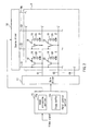
- FIG. 2 is a diagram illustrating a configuration of the liquid crystal panel shown in FIG. 1 .
- the liquid crystal display device 1 ( FIG. 1 ) is provided with a panel control portion 15 that performs drive control of the liquid crystal panel 2 ( FIG. 1 ) as the display portion that displays information such as characters and images, and a source driver 16 and a gate driver 17 that are operated based on instruction signals from the panel control portion 15.
- a panel control portion 15 that performs drive control of the liquid crystal panel 2 ( FIG. 1 ) as the display portion that displays information such as characters and images
- a source driver 16 and a gate driver 17 that are operated based on instruction signals from the panel control portion 15.
- the panel control portion 15 is placed in the control device and receives video signals from outside of the liquid crystal display device 1. Further, the panel control portion 15 includes an image processing portion 15a that performs predetermined image processing on input video signals so as to generate respective instruction signals to the source driver 16 and the gate driver 17, and a frame buffer 15b that can store one frame of display data contained in the input video signals. The panel control portion 15 performs drive control of the source driver 16 and the gate driver 17 in accordance with input video signals, whereby information in accordance with the video signals is displayed on the liquid crystal panel 2.
- the source driver 16 and the gate driver 17 are disposed on the active matrix substrate 5. Specifically, on a surface of the active matrix substrate 5, the source driver 16 is disposed along the horizontal direction of the liquid crystal panel 2 in an outside region of an effective display area A of the liquid crystal panel 2 as a display panel. Further, the gate driver 17 is disposed along the vertical direction of the liquid crystal panel 2 in the outside region of the effective display area A on the surface of the active matrix substrate 5.
- the source driver 16 and the gate driver 17 are drive circuits that drive, on a pixel basis, a plurality of pixels P placed on the liquid crystal panel 2 side.
- the source diver 16 and the gate driver 17 respectively are connected to a plurality of source lines S1-SM (M is an integer of 2 or more; hereinafter, referred to as "S” collectively) and a plurality of gate lines G1-GN (N is an integer of 2 or more; hereinafter, referred to as "G” collectively).
- the source lines S and the gate lines G respectively constitute data lines and scanning lines that are arranged in a matrix so as to cross each other on a base material (not shown) made of a transparent glass material or a transparent synthetic resin contained in the active matrix substrate 5.
- the source lines S are formed on the base material so as to be parallel to a column direction in the matrix (the vertical direction of the liquid crystal panel 2) and the gate lines G are formed on the base material so as to be parallel to a row direction in the matrix (the horizontal direction of the liquid crystal panel 2).
- a thin film transistor 18 as a switching element and a pixel P that has a pixel electrode 19 connected to the thin film transistor 18 are provided. Further, in each of the pixels P, a common electrode 20 is opposed to the pixel electrode 19, with the liquid crystal layer of the liquid crystal panel 2 being interposed therebetween. In other words, in the active matrix substrate 5, the thin film transistor 18, the pixel electrode 19 and the common electrode 20 are provided per pixel.
- the plurality of pixels P include red (R), green (G) and blue (B) pixels.
- the RGB pixels are arranged sequentially in parallel to the gate lines G1-GN in this order, for example. Further, the RGB pixels can display corresponding color by color filter layers (not shown) provided on the color filter substrate 4 side.
- the gate driver 17 sequentially outputs scanning signals (gate signals) with respect to the gate lines G1-GN so as to bring gate electrodes of the corresponding thin film transistors 18 to an ON state based on instruction signals from the image processing portion 15a.
- the source driver 16 outputs data signals (voltage signals (gradation voltage)) in accordance with brightness (gradation) of the display image with respect to the corresponding source lines S1-SM, based on instruction signals from the image processing portion 15a.
- FIG. 3 is a view illustrating a configuration of main portions of the active matrix substrate shown in FIG. 1 .
- FIG. 4 is a cross-sectional view taken along a line IV-IV in FIG. 3 .
- the thin film transistor 18 and the pixel electrode 19 are disposed per pixel P.
- the thin film transistor 18 includes a source electrode 18s provided integrally with the source line S, a drain electrode 18d provided to be opposed to the source electrode 18s, and a semiconductor layer SL and a gate electrode 18g provided sequentially under the source electrode 18s and the drain electrode 18d.
- the gate electrode 18g is provided integrally with the gate line G.
- the drain electrode 18d is formed of one end portion of a three-layered metal film 21, which is provided as a metal film described later.
- auxiliary capacitance lines CS are disposed parallel to the gate lines G so as to pass substantially the center of the pixels P between two adjacent gate lines G.
- An auxiliary capacitance electrode 22 is disposed above the auxiliary capacitance line CS.
- the auxiliary capacitance electrode 22 is formed of the other end portion of the three-layered metal film 21.
- a contact hole portion H connecting the pixel electrode 19 and the three-layered metal film (metal film) 21 is formed above the auxiliary capacitance electrode 22.
- the pixel electrode 19 and the three-layered metal film 21 are connected to each other via an anodic oxidation film.
- a dimension of the contact hole portion H in the vertical direction (direction parallel to the source lines S) and a dimension thereof in the horizontal direction (direction parallel to the gate lines G) are set at 30 ⁇ m, for example.
- the thin film transistor 18 ( FIG. 3 ), the auxiliary capacitance line CS, the auxiliary capacitance electrode 22 ( FIG. 3 ) and the contact hole portion H are formed.
- the gate electrode 18g composed of a three-layered metal film having a titanium layer 23a, an aluminum layer 23b and a titanium layer 23c is disposed on the base material 5a. Further, a gate insulating film 24 is disposed over the gate electrode 18g, and the semiconductor layer SL is disposed on the gate insulating film 24. Contact layers 26a and 26b, which are connected to a source region and a drain region of the semiconductor layer SL, respectively, are disposed on the semiconductor layer SL.
- the gate electrode 18g may be formed using a single metal film to which pure metal or impurity is added, or other multi-layered metal film.
- the drain electrode 18d ( FIG. 3 ) of the thin film transistor 18 is disposed above the contact layer 26b. As described above, one end portion of the three-layered metal film 21 as the metal film connecting the drain electrode 18d and the pixel electrode 19 is used as the drain electrode 18d. Further, a three-layered metal film having a titanium layer 25a, an aluminum layer 25b and a titanium layer 25c, for example, is used as the three-layered metal film 21.
- the source electrode 18s of the thin film transistor 18 is disposed above the contact layer 26a.
- the same metal film as the three-layered metal film 21 is used for the source electrode 18s.
- the source electrode 18s is formed of one end portion of a three-layered metal film having a titanium layer 25a', an aluminum layer 25b' and a titanium layer 25c', for example. Further, the other end portion of the metal film is formed integrally with the source line S ( FIG. 3 ).
- a protective layer 27 is disposed over the three-layered metal film 21 and the three-layered metal film having the titanium layer 25a', the aluminum layer 25b' and the titanium layer 25c'. Further, the protective layer 27 is formed also on a channel region of the semiconductor layer SL between the contact layers 26a and 26b.
- an insulating layer 28 as an (interlayer) insulating film is disposed on the protective layer 27.
- the auxiliary capacitance line CS composed of the same three-layered metal film as that of the gate electrode 18g, for example, is disposed on the base material 5a.
- the auxiliary capacitance line CS is formed of a three-layered metal film having a titanium layer 23a', an aluminum layer 23b' and a titanium layer 23c', for example.
- the gate insulating film 24 is disposed over the auxiliary capacitance line CS, and the semiconductor layer SL and the contact layer 26 are disposed sequentially on the gate insulating film 24.
- the auxiliary capacitance line CS may be formed using a single metal film to which pure metal or impurity is added, or other multi-layered metal film.
- auxiliary capacitance electrode 22 ( FIG. 3 ) formed of the other end portion of the three-layered metal film 21 is disposed above the contact layer 26.
- the auxiliary capacitance electrode 22 and the auxiliary capacitance line CS are connected to each other by capacitive coupling via the gate insulating film 24, the semiconductor layer SL, and the contact layer 26.
- an anodic oxidation film 29 i.e., titanium oxide
- anodically oxidizing the upper titanium layer 25c is formed on the three-layered metal film 21.
- the anodic oxidation film 29 is formed so as to fill a contact hole of the protective layer 27, with an end portion of the anodic oxidation film 29 being placed under the insulating layer 28. Further, in the contact hole portion H, the anodic oxidation film 29 is connected to the pixel electrode 19.
- the auxiliary capacitance electrode 22 and the auxiliary capacitance line CS may be connected to each other by capacitive coupling via the gate insulating film 24.
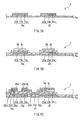
- FIG. 5 includes views illustrating production processes of the active matrix substrate, and FIGS. 5A to 5C illustrate a series of the main production processes.
- FIG. 6 includes views illustrating production processes of the active matrix substrate, and FIGS. 6A and 6B illustrate a series of the main production processes to be performed after the processes shown in FIG. 5C .
- a three-layered metal film having a titanium layer 23a, an aluminum layer 23b and a titanium layer 23c, and a three-layered metal film having a titanium layer 23a', an aluminum layer 23b' and a titanium layer 23c' are formed on a base material 5a by a sputtering method, for example.
- Specific thicknesses of the titanium layers 23a, 23a', the aluminum layers 23b, 23b' and the titanium layers 23c, 23c' respectively are 30 nm, 250 nm and 150 nm, for example.
- a gate electrode 18g and an auxiliary capacitance line CS are formed on the base material 5a. Further, at this time, gate lines G are formed on the base material 5a simultaneously.
- a specific thickness of the gate insulating film 24 is 400 nm, for example.
- a semiconductor layer SL made of an amorphous silicon (a-Si) film and an n+ amorphous silicon layer 26 doped with phosphorus (P), for example are laminated above the gate electrode 18g and the auxiliary capacitance line CS, and patterned so as to have a cross section shown in FIG. 5B .
- Specific thicknesses of the semiconductor layer SL and the n+ amorphous silicon layer 26 respectively are 200 nm and 50 nm, for example.
- a three-layered metal film 21 having a titanium layer 25a, an aluminum layer 25b and a titanium layer 25c is formed.
- a source electrode 18s and a drain electrode 18d are formed.
- one end portion of the three-layered metal film 21 is configured as the drain electrode 18d
- an end portion of a three-layered metal film having a titanium layer 25a', an aluminum layer 25b' and a titanium layer 25c' and being separated from the drain electrode 18d by a predetermined distance is configured as the source electrode 18s.
- the other end portion of the three-layered metal film 21 is configured as an auxiliary capacitance electrode 22.
- a metal film forming process is completed in which a metal film connecting the drain electrode 18d of the thin film transistor 18 and the pixel electrode 19 is formed on the base material 5a.
- Specific thicknesses of the titanium layers 25a, 25a', the aluminum layers 25b, 25b' and the titanium layers 25c, 25c' respectively are 40 nm, 250 nm and 200 nm, for example.
- a channel region is formed in the semiconductor layer SL.
- the source electrode 18s that is formed of the end portion of the three-layered metal film having the titanium layer 25a', the aluminum layer 25b' and the titanium layer 25c' is connected to a source region of the semiconductor layer SL via the contact layer 26a.
- the drain electrode 18d that is formed of one end portion of the three-layered metal film 21 having the titanium layer 25a, the aluminum layer 25b and the titanium layer 25c is connected to a drain region of the semiconductor layer SL via the contact layer 26b. Further, in a region above the channel region of the semiconductor layer SL, the n+ amorphous silicon layer 26 and the three-layered metal film 21 are removed.
- a silicon nitride (SiNx) layer for example, is formed over the source electrode 18s and the drain electrode 18d so as to cover the three-layered metal film 21, whereby a protective layer 27 is formed.
- SiNx silicon nitride
- a protective layer forming process is completed in which the protective layer 27 is formed so as to cover the three-layered metal film (metal film) 21.
- a specific thickness of the protective layer 27 is 80 nm, for example.
- an (interlayer) insulating layer 28 made of a transparent resin is formed on the protective layer 27.
- a specific thickness of the insulating layer 28 is 3000 nm, for example.
- a contact hole 28h of the contact hole portion H is formed in the insulating layer 28.
- an insulating layer forming process is completed in which the insulating layer 28 is formed on the protective layer 27 so as to be provided with the contact hole 28h of the contact hole portion H connecting the pixel electrode 19 and the three-layered metal film (metal layer) 21.
- a contact hole 27h of the contact hole portion H is formed in the protective layer 27.
- a contact hole forming process is completed in which the contact hole 27h of the contact hole portion H is formed in the protective layer 27 using the insulating layer 28 as a mask.
- the titanium layer 25c on the upper side of the three-layered metal film 21 is exposed.
- an anodic oxidation film 29 is formed in the contact hole portion H. Specifically, by anodically oxidizing the upper titanium layer 25c at a formation voltage of 80 V using a 1% phosphoric acid aqueous solution, for example, the anodic oxidation film 29 made of titanium oxide is formed.
- an anodic oxidation film forming process is completed in which the anodic oxidation film 29 is formed on the three-layered metal film (metal film) 21 so as to fill the contact hole 27h of the protective layer 27 with an end portion of the anodic oxidation film 29 being placed under the insulating layer 28, by anodically oxidizing the three-layered metal film (metal film) 21 that is exposed in the contact hole 27h formed in the protective layer 27.
- a volume of the titanium layer 25c expands, whereby the anodic oxidation film 29 (titanium oxide layer) 29 is formed. Therefore, as shown in FIG. 6B , no step difference is formed between the insulating layer 28 and the anodic oxidation film 29, which avoids disconnection of the pixel electrode 19 in the contact hole portion H.
- the pixel electrode 19 is formed above the thin film transistor 18 and the auxiliary capacitance electrode 22.
- a connecting process is completed in which the pixel electrode 19 and the three-layered metal film (metal film) 21 are connected to each other via the anodic oxidation film 29 in the contact hole portion H.
- a specific thickness of the pixel electrode 19 is 130 nm.
- the anodic oxidation film 29 is formed on the three-layered metal film (metal film) 21 so as to fill the contact hole 27h of the protective layer 27, with an end portion of the anodic oxidation film 29 being placed under the insulating layer 28. Further, in the contact hole portion H, the pixel electrode 19 and the three-layered metal film 21 are connected to each other via the anodic oxidation film 29.
- step coverage can be performed with respect to undercut in the protective layer 27 without removing the insulating layer in the periphery of the contact hole of the protective layer to expose a borderline of the protective layer in the contact hole. Consequently, in the present embodiment, unlike the conventional example, the production process of the active matrix substrate 5 can be simplified.
- the volume of the titanium layer 25c is expanded so that the anodic oxidation film 29 is formed to eliminate the step difference between the insulating layer 28 and the anodic oxidation film 29.
- the occurrence of disconnection of the pixel electrode 19 in the contact hole portion H, etc. can be avoided, which makes it possible to easily configure the active matrix substrate 5 with excellent reliability.
- liquid crystal display device (display device) 1 produced simply can be configured easily.
- the present invention is applied to a transmission type liquid crystal display device.
- the display device of the present invention is not particularly limited as long as an active matrix substrate is used as the display device.
- the display device of the present invention can be applied to various display devices using an active matrix substrate, such as a semi-transmission type or reflection type liquid crystal panel, an organic electronic luminescence (EL) element, an inorganic EL element, and a field emission display.
- an active matrix substrate such as a semi-transmission type or reflection type liquid crystal panel, an organic electronic luminescence (EL) element, an inorganic EL element, and a field emission display.
- a three-layered metal film having a titanium layer, an aluminum layer and a titanium layer is used as the metal film, and a titanium oxide (anodic oxidation film) formed by anodically oxidizing the upper titanium layer is used.
- the active matrix substrate of the present invention is not particularly limited as long as an anodic oxidation film is formed on the metal film in the contact hole portion by anodically oxidizing the metal film so as to fill the contact hole of the protective layer with an end portion of the anodic oxidation film being placed under the insulating layer, and the pixel electrode and the metal film are connected to each other via the anodic oxidation film in the contact hole portion.
- a three-layered metal film having a niobium layer, an aluminum layer and a titanium layer may be used as the metal film, and a niobium oxide (anodic oxidation film) formed by anodically oxidizing the upper niobium layer may be used.
- a three-layered metal film having a titanium layer or a niobium layer and an aluminum layer may be used as the metal film, and a titanium oxide or a niobium oxide may be used as an anodic oxide.
- titanium or niobium may be used as the metal film, and a titanium oxide or a niobium oxide may be used as the anodic oxide.
- titanium or niobium to which predetermined impurity is added may be used as the metal film, and an anodic oxide of the metal may be used. Note that the case where an anodic oxidation film of titanium or niobium is used is preferred, because the metal film and the pixel electrode can be electrically connected to each other reliably.
- one end portion and the other end portion of the three-layered metal film are used as the drain electrode and the auxiliary capacitance electrode, respectively.
- the present invention is not limited thereto, and one end portion and the other end portion of the metal film, the drain electrode and the auxiliary capacitance electrode can be configured separately. In other words, the present invention can be applied to an active matrix substrate not provided with the auxiliary capacitance electrode.
- the case where an end portion of the metal film is used as the drain electrode or auxiliary capacitance electrode is preferred because an active matrix substrate produced more simply can be configured, which makes it possible to simplify the production process easily.
- the case where one end portion and the other end portion of the metal film are used as the drain electrode and the auxiliary capacitance electrode, respectively is preferred because an active matrix substrate produced further simply can be configured in the active matrix substrate having the auxiliary capacitance electrode, which makes it possible to simplify the production process more easily.
- the present invention is useful with respect to an active matrix substrate whose production process can be simplified, a production method thereof, and a display device using the active matrix substrate.
Landscapes
- Physics & Mathematics (AREA)
- Nonlinear Science (AREA)
- Mathematical Physics (AREA)
- Engineering & Computer Science (AREA)
- Chemical & Material Sciences (AREA)
- Crystallography & Structural Chemistry (AREA)
- Microelectronics & Electronic Packaging (AREA)
- General Physics & Mathematics (AREA)
- Optics & Photonics (AREA)
- Devices For Indicating Variable Information By Combining Individual Elements (AREA)
- Liquid Crystal (AREA)
- Thin Film Transistor (AREA)
- Internal Circuitry In Semiconductor Integrated Circuit Devices (AREA)
Abstract
Disclosed is an active matrix substrate (5) on which pixels, each having a thin film transistor (18) and a pixel electrodes (19) connected to the thin film transistor (18), are disposed in a matrix, and that includes a base material (5a) on which the pixels in a matrix are formed. In a contact hole portion (H), by anodically oxidizing a three-layered metal film (metal film) (21), an anodic oxidation film (29) is formed on the three-layered metal film (21) so as to fill a contact hole of a protective layer (27), with an end portion of the anodic oxidation film (29) being placed under an insulating layer (28). In the contact hole portion (H), the pixel electrode (19) and the three-layered metal film (21) are connected to each other via the anodic oxidation film (29).
Description
- The present invention relates to an active matrix substrate on which pixels are disposed in a matrix, a production method thereof, and a display device using the active matrix substrate.
- Recently, for example, a liquid crystal display device has been used widely in a liquid crystal television, a monitor, a mobile phone, etc., as a flat panel display that has features such as a smaller thickness and a lighter weight as compared with a conventional Braun tube. A known liquid crystal display device of this kind uses, in a liquid crystal panel as a display panel, an active matrix substrate in which a plurality of data lines (source lines) and a plurality of scanning lines (gate lines) are arranged in a matrix, and pixels, each having a TFT (Thin Film Transistor) as a switching element and a pixel electrode connected to the thin film transistor, are arranged in a matrix in the vicinities of intersections of the data lines and the scanning lines.
- In the active matrix substrate as described above, the pixel electrode and a drain electrode of the thin film transistor are connected to each other via a contact hole portion. Specifically, in the active matrix substrate, generally, a protective layer is formed on the thin film transistor, and an (interlayer) insulating layer is formed on the protective layer. Further, in the contact hole portion of the active matrix substrate, by providing a contact hole in each of the protective layer and the insulating layer, the pixel electrode and the drain electrode are brought into contact with each other, whereby these electrodes are connected to each other.
- Further, in the conventional active matrix substrate, generally, the contact hole of the protective layer is formed by etching the protective layer, using the insulating layer formed with the contact hole as a mask. However, in the conventional active matrix substrate, the protective layer sometimes is undercut excessively under the insulating layer during the etching, which makes a profile of the pixel electrode worse, disconnects the pixel electrode due to an improper connection of the pixel electrode to the drain electrode, etc.
- Therefore, in the conventional active matrix substrate, as described in Patent Document 1 below, for example, after forming the contact hole of the protective layer by the etching, the insulating layer in the periphery of the contact hole of the protective layer is removed by performing an ashing process to expose a borderline of the protective layer in the contact hole. Thus, in this conventional active matrix substrate, an undercut structure caused in the protective layer is removed. It also is indicated that, in the contact hole portion of this conventional active matrix substrate, by forming a sidewall around the contact hole of the insulating layer and a sidewall around the contact hole of the protective layer in, for example, a stepped configuration, the occurrence of the above problems are suppressed further.
- Patent Document 1:
JP 2005-510064 A - However, in the conventional active matrix substrate as described above, the production process cannot be simplified.
- Specifically, in the conventional active matrix substrate, after forming the contact hole of the protective layer, the insulating layer in the periphery of the contact hole of the protective layer is removed by performing the ashing process to expose the borderline of the protective layer in the contact hole. However, in this conventional active matrix substrate, in order to expose the borderline of the protective layer, it takes considerable time and labor to perform the ashing process, which prevents the production process from being simplified. Especially, in the conventional active matrix substrate, when forming the sidewall around the contact hole of the insulating layer and the sidewall around the contact hole of the protective layer in the stepped configuration, the ashing process need be performed with high precision, which prevents the production process from being simplified.
- In view of the above problem, it is an object of the present invention to provide an active matrix substrate whose production process can be simplified, a production method thereof, and a display device using the active matrix substrate.
- The achieve the above object, an active matrix substrate according to the present invention is an active matrix substrate on which pixels, each having a thin film transistor and a pixel electrode connected to the thin film transistor, are disposed in a matrix, and that includes a base material on which the pixels in a matrix are formed. On the base material, a metal film connecting a drain electrode of the thin film transistor and the pixel electrode, a protective layer formed so as to cover the metal film, and a insulating layer formed on the protective layer are disposed. In each of the protective layer and the insulating layer, a contact hole of a contact hole portion connecting the pixel electrode and the metal film is provided. In the contact hole portion, an anodic oxidation film is formed on the metal film by anodically oxidizing the metal film so as to fill the contact hole of the protective layer with an end portion of the anodic oxidation film being placed under the insulating layer. In the contact hole portion, the pixel electrode and the metal film are connected to each other via the anodic oxidation film.
- In the active matrix substrate configured as above, the anodic oxidation film is formed on the metal film so as to fill the contact hole of the protective layer, with an end portion of the anodic oxidation film being placed under the insulating layer. Further, in the contact hole portion, the pixel electrode and the metal film are connected to each other via the anodic oxidation film. Thereby, unlike the above conventional example, the production process can be simplified.
- Further, in the above active matrix substrate, it is preferable that an end portion of the metal film is used as the drain electrode.
- In this case, since the end portion of the metal film doubles as the drain electrode, an active matrix substrate produced more simply can be configured, whereby the production process can be simplified easily.
- Further, in the above active matrix substrate, it is preferable that, on the base material, an auxiliary capacitance electrode for generating auxiliary capacitance is provided on the pixel basis, and an end portion of the metal film is used as the auxiliary capacitance electrode.
- In this case, since the end portion of the metal film doubles as the auxiliary capacitance electrode, an active matrix substrate produced more simply can be configured in the active matrix substrate having the auxiliary capacitance electrode, whereby the production process can be simplified easily.
- Further, in the above active matrix substrate, it is preferable that the metal film contains titanium or niobium, and the anodic oxidation film includes an anodic oxidation film of titanium or niobium.
- In this case, since the anodic oxidation film of titanium or niobium is used, the metal film and the pixel electrode can be electrically connected to each other reliably.
- Further, a display device of the present invention uses the active matrix substrate according to any one of the above configurations.
- In the display device configured as above, since the active matrix substrate whose production process can be simplified is used, a display device produced simply can be configured easily.
- Further, a method for producing an active matrix substrate of the present invention is a method for producing an active matrix substrate on which pixels, each having a thin film transistor and a pixel electrode connected to the thin film transistor, are disposed in a matrix, and that includes a base material on which the pixels in a matrix are formed, including: a metal film forming process in which a metal film connecting a drain electrode of the thin film transistor and the pixel electrode is formed on the base material; a protective layer forming process in which a protective layer is formed so as to cover the metal film; an insulating layer forming process in which an insulating layer is formed on the protective layer so as to be provided with a contact hole of a contact hole portion connecting the pixel electrode and the metal film; a contact hole forming process in which a contact hole of the contact hole portion is formed in the protective layer using the insulating layer as a mask; an anodic oxidation film forming process in which an anodic oxidation film is formed on the metal film so as to fill the contact hole of the protective layer with an end portion of the anodic oxidation film being placed under the insulating layer, by anodically oxidizing the metal film that is exposed in the contact hole formed in the protective layer; and a connecting process in which the pixel electrode and the metal film are connected to each other via the anodic oxidation film in the contact hole portion.
- In the method for producing an active matrix substrate configured as above, in the anodic oxidation film forming process, by anodically oxidizing the metal film that is exposed in the contact hole formed in the protective layer, the anodic oxidation film is formed on the metal film so as to fill the contact hole of the protective layer, with an end portion of the anodic oxidation film being placed under the insulating layer. Further, in the connecting process, in the contact hole portion, the pixel electrode and the metal film are connected to each other via the anodic oxidation film. Thereby, unlike the above conventional example, it is unnecessary to remove the insulating layer in the periphery of the contact hole of the protective layer to expose a borderline of the protective layer in the contact hole. Consequently, unlike the above conventional example, the production process of the active matrix substrate can be simplified.
- Further, in the method for producing the active matrix substrate, it is preferable that, in the metal film forming process, an end portion of the metal film is formed as the drain electrode.
- In this case, since the end portion of the metal film doubles as the drain electrode, an active matrix substrate produced more simply can be configured, whereby the production process can be simplified easily.
- Further, in the method for producing the active matrix substrate, it is preferable that, in the metal film forming process, an end portion of the metal film is provided on the pixel basis, and formed as an auxiliary capacitance electrode for generating auxiliary capacitance.
- In this case, since the end portion of the metal film doubles as the auxiliary capacitance electrode, an active matrix substrate produced more simply can be configured in the active matrix substrate having the auxiliary capacitance electrode, whereby the production process can be simplified easily.
- Further, in the method for producing the active matrix substrate, it is preferable that the metal film contains titanium or niobium, and the anodic oxidation film includes an anodic oxidation film of titanium or niobium.
- In this case, since the anodic oxidation film of titanium or niobium is used, the metal film and the pixel electrode can be electrically connected to each other reliably.
- According to the present invention, it is possible to provide an active matrix substrate whose production process can be simplified, a production method thereof, and a display device using the active matrix substrate.
-
- [
FIG. 1] FIG. 1 is a view illustrating a liquid crystal display device according to one embodiment of the present invention. - [
FIG. 2] FIG. 2 is a diagram illustrating a configuration of a liquid crystal panel shown inFIG. 1 . - [
FIG. 3] FIG. 3 is a view illustrating a configuration of main portions of an active matrix substrate shown inFIG. 1 . - [
FIG. 4] FIG. 4 is a cross-sectional view taken along a line IV-IV inFIG. 3 . - [
FIG. 5] FIG. 5 includes views illustrating production processes of the active matrix substrate, andFIGS. 5A to 5C illustrate a series of the main production processes. - [
FIG. 6] FIG. 6 includes views illustrating production processes of the active matrix substrate, andFIGS. 6A and 6B illustrate a series of the main production processes to be performed after the processes shown inFIG. 5C . - Hereinafter, preferred embodiments of an active matrix substrate, a production method thereof, and a display device of the present invention will be described with reference to the drawings. In the following description, the present invention is applied to a transmission-type liquid crystal display device. The dimensions of constituent members in the drawings do not faithfully reflect the actual dimensions of constituent members, dimension ratio of the respective constituent members, etc.
-
FIG. 1 is a view illustrating a liquid crystal display device according to one embodiment of the present invention. InFIG. 1 , a liquid crystal display device 1 of the present embodiment is provided with aliquid crystal panel 2 and a backlight device 3. An upper side of theliquid crystal panel 2 inFIG. 1 is defined as a viewing side (display surface side). The backlight device 3 is arranged on a non-display surface side (lower side inFIG. 1 ) of theliquid crystal panel 2 and generates illumination light for illuminating theliquid crystal panel 2. - The
liquid crystal panel 2 includes a color filter substrate 4 and anactive matrix substrate 5 of the present invention that constitute a pair of substrates, andpolarizing plates 6, 7 that are provided on outer surfaces of the color filter substrate 4 and theactive matrix substrate 5, respectively. A liquid crystal layer (not shown) is sandwiched between the color filter substrate 4 and theactive matrix substrate 5. The color filter substrate 4 and theactive matrix substrate 5 are made of a flat plate-shaped transparent glass material or a transparent synthetic resin such as an acrylic resin. Thepolarizing plates 6, 7 are made of a resin film such as TAC (triacetyl cellulose) or PVA (polyvinyl alcohol). Thepolarizing plates 6, 7 are bonded to the corresponding color filter substrate 4 oractive matrix substrate 5 so as to cover at least an effective display region of a display surface of theliquid crystal panel 2. - The
active matrix substrate 5 constitutes one of the pair of substrates and includes pixel electrodes, TFTs (Thin Film Transistor), etc., that are formed between theactive matrix substrate 5 and the liquid crystal layer in accordance with a plurality of pixels included in the display surface of the liquid crystal panel 2 (detailed later). Meanwhile, the color filter substrate 4 constitutes the other of the pair of substrates and includes color filters, common electrodes, etc., that are formed between the color filter substrate 4 and the liquid crystal layer (not shown). - Further, the
liquid crystal panel 2 is provided with a FPC (Flexible Printed Circuit) 8 that is connected to a control device (not shown) that performs drive control of theliquid crystal panel 2. The display surface is driven on a pixel basis by operating the liquid crystal layer on a pixel basis, whereby a desired image can be displayed on the display surface. - Note that the
liquid crystal panel 2 can have any liquid crystal mode and any pixel structure. Theliquid crystal panel 2 also can have any drive mode. In other words, any liquid crystal panel capable of displaying information can be used as theliquid crystal panel 2. Therefore, a detailed structure of theliquid crystal panel 2 is not illustrated inFIG. 1 , and a description thereof is omitted. - The backlight device 3 includes a light-emitting
diode 9 as a light source, and a light-guidingplate 10 that is arranged to be opposed to the light-emittingdiode 9. Further, in the backlight device 3, the light-emittingdiode 9 and the light-guidingplate 10 are sandwiched by abezel 14 having an L-shape in cross section, with theliquid crystal panel 2 being located above the light-guidingplate 10. Further, acase 11 is mounted on the color filter substrate 4. Thus, the backlight device 3 is attached to theliquid crystal panel 2, and they are integrated as the transmission-type liquid crystal display device 1 in which illumination light from the backlight device 3 enters theliquid crystal panel 2. - The light-guiding
plate 10 is made of a synthetic resin such as a transparent acrylic resin and receives light from the light-emittingdiode 9. A reflectingsheet 12 is disposed on a surface of the light-guidingplate 10 on a side opposite to theliquid crystal panel 2 side (opposed surface side). Further,optical sheets 13 such as a lens sheet and a diffusion sheet are provided on a surface of the light-guidingplate 10 on theliquid crystal panel 2 side (light-emitting surface side). Light from the light-emittingdiode 9 that is guided inside the light-guidingplate 10 in a predetermined light-guiding direction (direction from the left side to the right side inFIG. 1 ) is transformed into planar illumination light having a uniform brightness, and given to theliquid crystal panel 2. - In the above description, the edge-light type backlight device 3 having the light-guiding
plate 10 is used. However, the present embodiment is not limited to this, and a direct type backlight device may be used. Further, a backlight device having a light source other than light-emitting diodes such as cold cathode fluorescent tubes and hot cathode fluorescent tubes also may be used. - Next, the
liquid crystal panel 2 of the present embodiment will be described specifically also with reference toFIG. 2 . -
FIG. 2 is a diagram illustrating a configuration of the liquid crystal panel shown inFIG. 1 . - In
FIG. 2 , the liquid crystal display device 1 (FIG. 1 ) is provided with apanel control portion 15 that performs drive control of the liquid crystal panel 2 (FIG. 1 ) as the display portion that displays information such as characters and images, and asource driver 16 and agate driver 17 that are operated based on instruction signals from thepanel control portion 15. - The
panel control portion 15 is placed in the control device and receives video signals from outside of the liquid crystal display device 1. Further, thepanel control portion 15 includes animage processing portion 15a that performs predetermined image processing on input video signals so as to generate respective instruction signals to thesource driver 16 and thegate driver 17, and aframe buffer 15b that can store one frame of display data contained in the input video signals. Thepanel control portion 15 performs drive control of thesource driver 16 and thegate driver 17 in accordance with input video signals, whereby information in accordance with the video signals is displayed on theliquid crystal panel 2. - The
source driver 16 and thegate driver 17 are disposed on theactive matrix substrate 5. Specifically, on a surface of theactive matrix substrate 5, thesource driver 16 is disposed along the horizontal direction of theliquid crystal panel 2 in an outside region of an effective display area A of theliquid crystal panel 2 as a display panel. Further, thegate driver 17 is disposed along the vertical direction of theliquid crystal panel 2 in the outside region of the effective display area A on the surface of theactive matrix substrate 5. - Further, the
source driver 16 and thegate driver 17 are drive circuits that drive, on a pixel basis, a plurality of pixels P placed on theliquid crystal panel 2 side. Thesource diver 16 and thegate driver 17 respectively are connected to a plurality of source lines S1-SM (M is an integer of 2 or more; hereinafter, referred to as "S" collectively) and a plurality of gate lines G1-GN (N is an integer of 2 or more; hereinafter, referred to as "G" collectively). The source lines S and the gate lines G respectively constitute data lines and scanning lines that are arranged in a matrix so as to cross each other on a base material (not shown) made of a transparent glass material or a transparent synthetic resin contained in theactive matrix substrate 5. In other words, the source lines S are formed on the base material so as to be parallel to a column direction in the matrix (the vertical direction of the liquid crystal panel 2) and the gate lines G are formed on the base material so as to be parallel to a row direction in the matrix (the horizontal direction of the liquid crystal panel 2). - Further, in the vicinity of each intersection between the source lines S and the gate lines G, a
thin film transistor 18 as a switching element and a pixel P that has apixel electrode 19 connected to thethin film transistor 18 are provided. Further, in each of the pixels P, acommon electrode 20 is opposed to thepixel electrode 19, with the liquid crystal layer of theliquid crystal panel 2 being interposed therebetween. In other words, in theactive matrix substrate 5, thethin film transistor 18, thepixel electrode 19 and thecommon electrode 20 are provided per pixel. - Further, in the
active matrix substrate 5, in the respective regions partitioned in a matrix by the source lines S and the gate lines G, a plurality of regions of the pixels P are formed. The plurality of pixels P include red (R), green (G) and blue (B) pixels. The RGB pixels are arranged sequentially in parallel to the gate lines G1-GN in this order, for example. Further, the RGB pixels can display corresponding color by color filter layers (not shown) provided on the color filter substrate 4 side. - Further, in the
active matrix substrate 5, thegate driver 17 sequentially outputs scanning signals (gate signals) with respect to the gate lines G1-GN so as to bring gate electrodes of the correspondingthin film transistors 18 to an ON state based on instruction signals from theimage processing portion 15a. Further, thesource driver 16 outputs data signals (voltage signals (gradation voltage)) in accordance with brightness (gradation) of the display image with respect to the corresponding source lines S1-SM, based on instruction signals from theimage processing portion 15a. - Next, a configuration of main portions of the
active matrix substrate 5 of the present embodiment will be described specifically also with reference toFIGS. 3 and4 . -
FIG. 3 is a view illustrating a configuration of main portions of the active matrix substrate shown inFIG. 1 .FIG. 4 is a cross-sectional view taken along a line IV-IV inFIG. 3 . - As shown in
FIG. 3 , in theactive matrix substrate 5, thethin film transistor 18 and thepixel electrode 19 are disposed per pixel P. Thethin film transistor 18 includes asource electrode 18s provided integrally with the source line S, adrain electrode 18d provided to be opposed to thesource electrode 18s, and a semiconductor layer SL and agate electrode 18g provided sequentially under thesource electrode 18s and thedrain electrode 18d. Thegate electrode 18g is provided integrally with the gate line G. Further, thedrain electrode 18d is formed of one end portion of a three-layeredmetal film 21, which is provided as a metal film described later. - Further, in the
active matrix substrate 5, auxiliary capacitance lines CS are disposed parallel to the gate lines G so as to pass substantially the center of the pixels P between two adjacent gate lines G. Anauxiliary capacitance electrode 22 is disposed above the auxiliary capacitance line CS. Further, theauxiliary capacitance electrode 22 is formed of the other end portion of the three-layeredmetal film 21. A contact hole portion H connecting thepixel electrode 19 and the three-layered metal film (metal film) 21 is formed above theauxiliary capacitance electrode 22. In the contact hole portion H, as described later, thepixel electrode 19 and the three-layeredmetal film 21 are connected to each other via an anodic oxidation film. Note that a dimension of the contact hole portion H in the vertical direction (direction parallel to the source lines S) and a dimension thereof in the horizontal direction (direction parallel to the gate lines G) are set at 30 µm, for example. - Further, in the
active matrix substrate 5, as shown inFIG. 4 , abase material 5a made of a non-alkali glass, for example, is used. On thebase material 5a, the thin film transistor 18 (FIG. 3 ), the auxiliary capacitance line CS, the auxiliary capacitance electrode 22 (FIG. 3 ) and the contact hole portion H are formed. - Specifically, the
gate electrode 18g composed of a three-layered metal film having atitanium layer 23a, analuminum layer 23b and atitanium layer 23c is disposed on thebase material 5a. Further, agate insulating film 24 is disposed over thegate electrode 18g, and the semiconductor layer SL is disposed on thegate insulating film 24. Contact layers 26a and 26b, which are connected to a source region and a drain region of the semiconductor layer SL, respectively, are disposed on the semiconductor layer SL. - Other than the above description, in place of the three-layered metal film having the
titanium layer 23a, thealuminum layer 23b and thetitanium layer 23c, thegate electrode 18g may be formed using a single metal film to which pure metal or impurity is added, or other multi-layered metal film. - Further, the
drain electrode 18d (FIG. 3 ) of thethin film transistor 18 is disposed above thecontact layer 26b. As described above, one end portion of the three-layeredmetal film 21 as the metal film connecting thedrain electrode 18d and thepixel electrode 19 is used as thedrain electrode 18d. Further, a three-layered metal film having atitanium layer 25a, analuminum layer 25b and atitanium layer 25c, for example, is used as the three-layeredmetal film 21. - The source electrode 18s of the
thin film transistor 18 is disposed above thecontact layer 26a. The same metal film as the three-layeredmetal film 21 is used for thesource electrode 18s. In other words, thesource electrode 18s is formed of one end portion of a three-layered metal film having atitanium layer 25a', analuminum layer 25b' and atitanium layer 25c', for example. Further, the other end portion of the metal film is formed integrally with the source line S (FIG. 3 ). Aprotective layer 27 is disposed over the three-layeredmetal film 21 and the three-layered metal film having thetitanium layer 25a', thealuminum layer 25b' and thetitanium layer 25c'. Further, theprotective layer 27 is formed also on a channel region of the semiconductor layer SL between the contact layers 26a and 26b. Moreover, an insulatinglayer 28 as an (interlayer) insulating film is disposed on theprotective layer 27. - Meanwhile, on the contact hole portion H side, the auxiliary capacitance line CS composed of the same three-layered metal film as that of the
gate electrode 18g, for example, is disposed on thebase material 5a. In other words, the auxiliary capacitance line CS is formed of a three-layered metal film having atitanium layer 23a', analuminum layer 23b' and atitanium layer 23c', for example. Further, thegate insulating film 24 is disposed over the auxiliary capacitance line CS, and the semiconductor layer SL and thecontact layer 26 are disposed sequentially on thegate insulating film 24. - Other than the above description, in place of the three-layered metal film having the
titanium layer 23a', thealuminum layer 23b' and thetitanium layer 23c', the auxiliary capacitance line CS may be formed using a single metal film to which pure metal or impurity is added, or other multi-layered metal film. - Further, the auxiliary capacitance electrode 22 (
FIG. 3 ) formed of the other end portion of the three-layeredmetal film 21 is disposed above thecontact layer 26. Theauxiliary capacitance electrode 22 and the auxiliary capacitance line CS are connected to each other by capacitive coupling via thegate insulating film 24, the semiconductor layer SL, and thecontact layer 26. Further, in the other end portion of the three-layered metal film 21 (auxiliary capacitance electrode 22), an anodic oxidation film 29 (i.e., titanium oxide) formed by anodically oxidizing theupper titanium layer 25c is formed on the three-layeredmetal film 21. Further, as shown inFIG. 4 , theanodic oxidation film 29 is formed so as to fill a contact hole of theprotective layer 27, with an end portion of theanodic oxidation film 29 being placed under the insulatinglayer 28. Further, in the contact hole portion H, theanodic oxidation film 29 is connected to thepixel electrode 19. - Other than the above description, without providing the semiconductor layer SL and the
contact layer 26, theauxiliary capacitance electrode 22 and the auxiliary capacitance line CS may be connected to each other by capacitive coupling via thegate insulating film 24. - Next, a method for producing main portions of the
active matrix substrate 5 of the present embodiment configured as above will be described specifically with reference toFIGS. 5 and6 . -
FIG. 5 includes views illustrating production processes of the active matrix substrate, andFIGS. 5A to 5C illustrate a series of the main production processes.FIG. 6 includes views illustrating production processes of the active matrix substrate, andFIGS. 6A and 6B illustrate a series of the main production processes to be performed after the processes shown inFIG. 5C . - As shown in
FIG. 5A , in theactive matrix substrate 5, first, a three-layered metal film having atitanium layer 23a, analuminum layer 23b and atitanium layer 23c, and a three-layered metal film having atitanium layer 23a', analuminum layer 23b' and atitanium layer 23c' are formed on abase material 5a by a sputtering method, for example. Specific thicknesses of thetitanium layers gate electrode 18g and an auxiliary capacitance line CS are formed on thebase material 5a. Further, at this time, gate lines G are formed on thebase material 5a simultaneously. - Next, as shown in
FIG. 5B , by a plasma CVD method, for example, agate insulating film 24 made of a silicon nitride (SiNx) film, for example, is formed so as to cover thegate electrode 18g and the auxiliary capacitance line CS on thebase material 5a. A specific thickness of thegate insulating film 24 is 400 nm, for example. Then, a semiconductor layer SL made of an amorphous silicon (a-Si) film and an n+amorphous silicon layer 26 doped with phosphorus (P), for example, are laminated above thegate electrode 18g and the auxiliary capacitance line CS, and patterned so as to have a cross section shown inFIG. 5B . Specific thicknesses of the semiconductor layer SL and the n+amorphous silicon layer 26 respectively are 200 nm and 50 nm, for example. - Next, as shown in
FIG. 5C , by a sputtering method, for example, a three-layeredmetal film 21 having atitanium layer 25a, analuminum layer 25b and atitanium layer 25c is formed. Then, by patterning the three-layeredmetal film 21, asource electrode 18s and adrain electrode 18d are formed. In other words, one end portion of the three-layeredmetal film 21 is configured as thedrain electrode 18d, and an end portion of a three-layered metal film having atitanium layer 25a', analuminum layer 25b' and atitanium layer 25c' and being separated from thedrain electrode 18d by a predetermined distance is configured as thesource electrode 18s. Further, the other end portion of the three-layeredmetal film 21 is configured as anauxiliary capacitance electrode 22. In this manner, a metal film forming process is completed in which a metal film connecting thedrain electrode 18d of thethin film transistor 18 and thepixel electrode 19 is formed on thebase material 5a. Specific thicknesses of thetitanium layers - After that, by removing the n+
amorphous silicon layer 26 by etching using thesource electrode 18s and thedrain electrode 18d as a mask, a channel region is formed in the semiconductor layer SL. In other words, as shown inFIG. 5C , thesource electrode 18s that is formed of the end portion of the three-layered metal film having thetitanium layer 25a', thealuminum layer 25b' and thetitanium layer 25c' is connected to a source region of the semiconductor layer SL via thecontact layer 26a. Further, thedrain electrode 18d that is formed of one end portion of the three-layeredmetal film 21 having thetitanium layer 25a, thealuminum layer 25b and thetitanium layer 25c is connected to a drain region of the semiconductor layer SL via thecontact layer 26b. Further, in a region above the channel region of the semiconductor layer SL, the n+amorphous silicon layer 26 and the three-layeredmetal film 21 are removed. - Next, as shown in
FIG. 6A , by a CVD method, for example, a silicon nitride (SiNx) layer, for example, is formed over thesource electrode 18s and thedrain electrode 18d so as to cover the three-layeredmetal film 21, whereby aprotective layer 27 is formed. In this manner, a protective layer forming process is completed in which theprotective layer 27 is formed so as to cover the three-layered metal film (metal film) 21. Further, a specific thickness of theprotective layer 27 is 80 nm, for example. - Next, as shown in
FIG. 6A , by a photolithography method, for example, an (interlayer) insulatinglayer 28 made of a transparent resin is formed on theprotective layer 27. A specific thickness of the insulatinglayer 28 is 3000 nm, for example. Further, acontact hole 28h of the contact hole portion H is formed in the insulatinglayer 28. In this manner, an insulating layer forming process is completed in which the insulatinglayer 28 is formed on theprotective layer 27 so as to be provided with thecontact hole 28h of the contact hole portion H connecting thepixel electrode 19 and the three-layered metal film (metal layer) 21. - Further, as shown in
FIG. 6A , in the contact hole portion H, by removing theprotective layer 27 by etching using the insulatinglayer 28 as a mask, acontact hole 27h of the contact hole portion H is formed in theprotective layer 27. In this manner, a contact hole forming process is completed in which thecontact hole 27h of the contact hole portion H is formed in theprotective layer 27 using the insulatinglayer 28 as a mask. After the completion of this process, in the contact hole portion H, thetitanium layer 25c on the upper side of the three-layeredmetal film 21 is exposed. - Next, as shown in
FIG. 6B , ananodic oxidation film 29 is formed in the contact hole portion H. Specifically, by anodically oxidizing theupper titanium layer 25c at a formation voltage of 80 V using a 1% phosphoric acid aqueous solution, for example, theanodic oxidation film 29 made of titanium oxide is formed. In this manner, an anodic oxidation film forming process is completed in which theanodic oxidation film 29 is formed on the three-layered metal film (metal film) 21 so as to fill thecontact hole 27h of theprotective layer 27 with an end portion of theanodic oxidation film 29 being placed under the insulatinglayer 28, by anodically oxidizing the three-layered metal film (metal film) 21 that is exposed in thecontact hole 27h formed in theprotective layer 27. In other words, by anodically oxidizing thetitanium layer 25c, a volume of thetitanium layer 25c expands, whereby the anodic oxidation film 29 (titanium oxide layer) 29 is formed. Therefore, as shown inFIG. 6B , no step difference is formed between the insulatinglayer 28 and theanodic oxidation film 29, which avoids disconnection of thepixel electrode 19 in the contact hole portion H. - Then, as shown in
FIG. 6B , by depositing a transparent conducting film such as ITO on the insulatinglayer 28 using a sputtering method, for example, and patterning the conducting film, thepixel electrode 19 is formed above thethin film transistor 18 and theauxiliary capacitance electrode 22. In this manner, a connecting process is completed in which thepixel electrode 19 and the three-layered metal film (metal film) 21 are connected to each other via theanodic oxidation film 29 in the contact hole portion H. Further, a specific thickness of thepixel electrode 19 is 130 nm. - In the
active matrix substrate 5 of the present embodiment configured as above, theanodic oxidation film 29 is formed on the three-layered metal film (metal film) 21 so as to fill thecontact hole 27h of theprotective layer 27, with an end portion of theanodic oxidation film 29 being placed under the insulatinglayer 28. Further, in the contact hole portion H, thepixel electrode 19 and the three-layeredmetal film 21 are connected to each other via theanodic oxidation film 29. Thereby, in theactive matrix substrate 5 of the present embodiment, unlike the conventional example, step coverage can be performed with respect to undercut in theprotective layer 27 without removing the insulating layer in the periphery of the contact hole of the protective layer to expose a borderline of the protective layer in the contact hole. Consequently, in the present embodiment, unlike the conventional example, the production process of theactive matrix substrate 5 can be simplified. - Further, in the present embodiment, by anodically oxidizing the
titanium layer 25c on the upper side of the three-layeredmetal film 21, the volume of thetitanium layer 25c is expanded so that theanodic oxidation film 29 is formed to eliminate the step difference between the insulatinglayer 28 and theanodic oxidation film 29. Thus, the occurrence of disconnection of thepixel electrode 19 in the contact hole portion H, etc., can be avoided, which makes it possible to easily configure theactive matrix substrate 5 with excellent reliability. - Further, since the
active matrix substrate 5 whose production process can be simplified is used in the present embodiment, a liquid crystal display device (display device) 1 produced simply can be configured easily. - The above embodiments are shown for illustrative purposes and are not limiting. The technical range of the present invention is defined by the claims, and all the modifications within the range equivalent to the configuration recited in the claims are also included in the technical range of the present invention.
- For example, in the above description, the present invention is applied to a transmission type liquid crystal display device. However, the display device of the present invention is not particularly limited as long as an active matrix substrate is used as the display device. Specifically, the display device of the present invention can be applied to various display devices using an active matrix substrate, such as a semi-transmission type or reflection type liquid crystal panel, an organic electronic luminescence (EL) element, an inorganic EL element, and a field emission display.
- Further, in the above description, a three-layered metal film having a titanium layer, an aluminum layer and a titanium layer is used as the metal film, and a titanium oxide (anodic oxidation film) formed by anodically oxidizing the upper titanium layer is used. However, the active matrix substrate of the present invention is not particularly limited as long as an anodic oxidation film is formed on the metal film in the contact hole portion by anodically oxidizing the metal film so as to fill the contact hole of the protective layer with an end portion of the anodic oxidation film being placed under the insulating layer, and the pixel electrode and the metal film are connected to each other via the anodic oxidation film in the contact hole portion.
- Specifically, a three-layered metal film having a niobium layer, an aluminum layer and a titanium layer may be used as the metal film, and a niobium oxide (anodic oxidation film) formed by anodically oxidizing the upper niobium layer may be used. Further, a three-layered metal film having a titanium layer or a niobium layer and an aluminum layer may be used as the metal film, and a titanium oxide or a niobium oxide may be used as an anodic oxide. Further, titanium or niobium may be used as the metal film, and a titanium oxide or a niobium oxide may be used as the anodic oxide. Moreover, for example, titanium or niobium to which predetermined impurity is added may be used as the metal film, and an anodic oxide of the metal may be used. Note that the case where an anodic oxidation film of titanium or niobium is used is preferred, because the metal film and the pixel electrode can be electrically connected to each other reliably.
- Further, in the above description, one end portion and the other end portion of the three-layered metal film (metal film) are used as the drain electrode and the auxiliary capacitance electrode, respectively. However, the present invention is not limited thereto, and one end portion and the other end portion of the metal film, the drain electrode and the auxiliary capacitance electrode can be configured separately. In other words, the present invention can be applied to an active matrix substrate not provided with the auxiliary capacitance electrode.
- Note that the case where an end portion of the metal film is used as the drain electrode or auxiliary capacitance electrode is preferred because an active matrix substrate produced more simply can be configured, which makes it possible to simplify the production process easily. Moreover, as in the above embodiment, the case where one end portion and the other end portion of the metal film are used as the drain electrode and the auxiliary capacitance electrode, respectively, is preferred because an active matrix substrate produced further simply can be configured in the active matrix substrate having the auxiliary capacitance electrode, which makes it possible to simplify the production process more easily.
- The present invention is useful with respect to an active matrix substrate whose production process can be simplified, a production method thereof, and a display device using the active matrix substrate.
-
- 1
- liquid crystal display device (display device)
- 5
- active matrix substrate
- 5a
- base material
- 18
- thin film transistor
- 18d
- drain electrode
- 19
- pixel electrode
- 21
- three-layered metal film (metal film)
- 25a
- titanium layer
- 25b
- aluminum layer
- 25c
- titanium layer
- 22
- auxiliary capacitance electrode
- 27
- protective layer
- 28
- insulating layer
Claims (9)
- An active matrix substrate on which pixels, each having a thin film transistor and a pixel electrode connected to the thin film transistor, are disposed in a matrix, and that includes a base material on which the pixels in a matrix are formed,
wherein, on the base material, a metal film connecting a drain electrode of the thin film transistor and the pixel electrode, a protective layer formed so as to cover the metal film, and a insulating layer formed on the protective layer are disposed,
in each of the protective layer and the insulating layer, a contact hole of a contact hole portion connecting the pixel electrode and the metal film is provided,
in the contact hole portion, an anodic oxidation film is formed on the metal film by anodically oxidizing the metal film so as to fill the contact hole of the protective layer with an end portion of the anodic oxidation film being placed under the insulating layer, and
in the contact hole portion, the pixel electrode and the metal film are connected to each other via the anodic oxidation film. - The active matrix substrate according to claim 1, wherein an end portion of the metal film is used as the drain electrode.
- The active matrix substrate according to claim 1,
wherein, on the base material, an auxiliary capacitance electrode for generating auxiliary capacitance is provided on the pixel basis, and
an end portion of the metal film is used as the auxiliary capacitance electrode. - The active matrix substrate according to any one of claims 1 to 3,
wherein the metal film contains titanium or niobium, and
the anodic oxidation film comprises an anodic oxidation film of titanium or niobium. - A display device using the active matrix substrate according to any one of claims 1 to 4.
- A method for producing an active matrix substrate on which pixels, each having a thin film transistor and a pixel electrode connected to the thin film transistor, are disposed in a matrix, and that includes a base material on which the pixels in a matrix are formed, comprising:a metal film forming process in which a metal film connecting a drain electrode of the thin film transistor and the pixel electrode is formed on the base material;a protective layer forming process in which a protective layer is formed so as to cover the metal film;an insulating layer forming process in which an insulating layer is formed on the protective layer so as to be provided with a contact hole of a contact hole portion connecting the pixel electrode and the metal film;a contact hole forming process in which a contact hole of the contact hole portion is formed in the protective layer using the insulating layer as a mask;an anodic oxidation film forming process in which an anodic oxidation film is formed on the metal film so as to fill the contact hole of the protective layer with an end portion of the anodic oxidation film being placed under the insulating layer, by anodically oxidizing the metal film that is exposed in the contact hole formed in the protective layer; anda connecting process in which the pixel electrode and the metal film are connected to each other via the anodic oxidation film in the contact hole portion.
- The method for producing the active matrix substrate according to claim 6, wherein, in the metal film forming process, an end portion of the metal film is formed as the drain electrode.
- The method for producing the active matrix substrate according to claim 6, wherein, in the metal film forming process, an end portion of the metal film is provided on the pixel basis, and formed as an auxiliary capacitance electrode for generating auxiliary capacitance.
- The method for producing the active matrix substrate according to any one of claims 6 to 8,
wherein the metal film contains titanium or niobium, and
the anodic oxidation film comprises an anodic oxidation film of titanium or niobium.
Applications Claiming Priority (2)
| Application Number | Priority Date | Filing Date | Title |
|---|---|---|---|
| JP2009272288 | 2009-11-30 | ||
| PCT/JP2010/069701 WO2011065204A1 (en) | 2009-11-30 | 2010-11-05 | Active matrix substrate, production method, and display device |
Publications (1)
| Publication Number | Publication Date |
|---|---|
| EP2509060A1 true EP2509060A1 (en) | 2012-10-10 |
Family
ID=44066307
Family Applications (1)
| Application Number | Title | Priority Date | Filing Date |
|---|---|---|---|
| EP10833051A Withdrawn EP2509060A1 (en) | 2009-11-30 | 2010-11-05 | Active matrix substrate, production method, and display device |
Country Status (4)
| Country | Link |
|---|---|
| US (1) | US8933452B2 (en) |
| EP (1) | EP2509060A1 (en) |
| JP (1) | JP5185447B2 (en) |
| WO (1) | WO2011065204A1 (en) |
Families Citing this family (4)
| Publication number | Priority date | Publication date | Assignee | Title |
|---|---|---|---|---|
| JP6124668B2 (en) | 2013-04-26 | 2017-05-10 | 三菱電機株式会社 | Thin film transistor substrate and manufacturing method thereof |
| JP6402914B2 (en) * | 2013-11-29 | 2018-10-10 | 日亜化学工業株式会社 | Method for manufacturing light emitting device |
| US10698864B2 (en) | 2017-11-13 | 2020-06-30 | Philo, Inc. | Auxiliary manifest file to provide timed metadata |
| KR102878049B1 (en) * | 2019-12-24 | 2025-10-29 | 엘지디스플레이 주식회사 | Display pannel and manufacturing method thereof |
Family Cites Families (7)
| Publication number | Priority date | Publication date | Assignee | Title |
|---|---|---|---|---|
| JP2000221488A (en) * | 1999-01-29 | 2000-08-11 | Sharp Corp | Liquid crystal display |
| JP3153203B2 (en) * | 1999-03-31 | 2001-04-03 | 株式会社半導体エネルギー研究所 | Active matrix type liquid crystal display |
| JP2001320039A (en) * | 2000-05-11 | 2001-11-16 | Canon Inc | Photoelectric conversion device |
| KR100796756B1 (en) | 2001-11-12 | 2008-01-22 | 삼성전자주식회사 | A contact portion of a semiconductor device, a method of manufacturing the same, and a thin film transistor array substrate for a display device including the same, and a method of manufacturing the same |
| CN103121799A (en) * | 2004-03-09 | 2013-05-29 | 出光兴产株式会社 | Sputtering target, transparent conductive film, thin film transistor, thin film transistor substrate, manufacturing method thereof, and liquid crystal display device |
| JP2006003776A (en) * | 2004-06-21 | 2006-01-05 | Seiko Epson Corp | Electro-optical device manufacturing method, electro-optical device, and electronic apparatus |
| JP2008241978A (en) * | 2007-03-27 | 2008-10-09 | Seiko Epson Corp | ELECTRO-OPTICAL DEVICE, MANUFACTURING METHOD THEREOF, AND ELECTRONIC DEVICE |
-
2010
- 2010-11-05 JP JP2011543193A patent/JP5185447B2/en not_active Expired - Fee Related
- 2010-11-05 EP EP10833051A patent/EP2509060A1/en not_active Withdrawn
- 2010-11-05 US US13/512,474 patent/US8933452B2/en not_active Expired - Fee Related
- 2010-11-05 WO PCT/JP2010/069701 patent/WO2011065204A1/en not_active Ceased
Non-Patent Citations (1)
| Title |
|---|
| See references of WO2011065204A1 * |
Also Published As
| Publication number | Publication date |
|---|---|
| JPWO2011065204A1 (en) | 2013-04-11 |
| US20120235149A1 (en) | 2012-09-20 |
| US8933452B2 (en) | 2015-01-13 |
| JP5185447B2 (en) | 2013-04-17 |
| WO2011065204A1 (en) | 2011-06-03 |
Similar Documents
| Publication | Publication Date | Title |
|---|---|---|
| US8779430B2 (en) | Semiconductor device, active matrix substrate, and display device | |
| US20120248450A1 (en) | Active matrix substrate and method for producing same | |
| US20120153289A1 (en) | Semiconductor device, active matrix substrate, and display device | |
| US20120256184A1 (en) | Semiconductor device, active matrix substrate and display device | |
| US8040482B2 (en) | Liquid crystal display | |
| KR100831091B1 (en) | Transflective liquid crystal display, flat panel display device, and electronic apparatus | |
| KR20190084189A (en) | Display device | |
| US9275932B2 (en) | Active matrix substrate, and display device | |
| US8933452B2 (en) | Active matrix substrate, production method, and display device | |
| US7697089B2 (en) | Liquid crystal display apparatus | |
| US9599866B2 (en) | Active matrix substrate and display device | |
| US20130293809A1 (en) | Array substrate for liquid crystal panel, and liquid crystal panel | |
| US20130102115A1 (en) | Method for manufacturing active matrix substrate | |
| CN100431158C (en) | Thin film transistor array substrate, semi-penetration semi-reflection display panel and display device | |
| US9690156B2 (en) | Active matrix substrate and display device | |
| JP2013250319A (en) | Active matrix substrate, manufacturing method, and display device | |
| JP2008139656A (en) | Display device and manufacturing method thereof | |
| US20210397056A1 (en) | Display device and method of repairing display device | |
| WO2026051676A1 (en) | Array substrate, display panel, and display device | |
| JP6503052B2 (en) | Liquid crystal display | |
| WO2012133157A1 (en) | Array substrate for liquid crystal panel and liquid crystal panel | |
| WO2014054487A1 (en) | Liquid crystal panel and method for manufacturing same | |
| JP2011059413A (en) | Display panel and manufacturing method |
Legal Events
| Date | Code | Title | Description |
|---|---|---|---|
| PUAI | Public reference made under article 153(3) epc to a published international application that has entered the european phase |
Free format text: ORIGINAL CODE: 0009012 |
|
| 17P | Request for examination filed |
Effective date: 20120604 |
|
| AK | Designated contracting states |
Kind code of ref document: A1 Designated state(s): AL AT BE BG CH CY CZ DE DK EE ES FI FR GB GR HR HU IE IS IT LI LT LU LV MC MK MT NL NO PL PT RO RS SE SI SK SM TR |
|
| DAX | Request for extension of the european patent (deleted) | ||
| STAA | Information on the status of an ep patent application or granted ep patent |
Free format text: STATUS: THE APPLICATION HAS BEEN WITHDRAWN |
|
| 18W | Application withdrawn |
Effective date: 20131129 |