EP2506411A1 - Charge pump circuit using low voltage transistors - Google Patents
Charge pump circuit using low voltage transistors Download PDFInfo
- Publication number
- EP2506411A1 EP2506411A1 EP12162766A EP12162766A EP2506411A1 EP 2506411 A1 EP2506411 A1 EP 2506411A1 EP 12162766 A EP12162766 A EP 12162766A EP 12162766 A EP12162766 A EP 12162766A EP 2506411 A1 EP2506411 A1 EP 2506411A1
- Authority
- EP
- European Patent Office
- Prior art keywords
- transfer transistor
- transistor
- internal node
- biasing
- charge pump
- Prior art date
- Legal status (The legal status is an assumption and is not a legal conclusion. Google has not performed a legal analysis and makes no representation as to the accuracy of the status listed.)
- Granted
Links
Images



Classifications
-
- H—ELECTRICITY
- H02—GENERATION; CONVERSION OR DISTRIBUTION OF ELECTRIC POWER
- H02M—APPARATUS FOR CONVERSION BETWEEN AC AND AC, BETWEEN AC AND DC, OR BETWEEN DC AND DC, AND FOR USE WITH MAINS OR SIMILAR POWER SUPPLY SYSTEMS; CONVERSION OF DC OR AC INPUT POWER INTO SURGE OUTPUT POWER; CONTROL OR REGULATION THEREOF
- H02M3/00—Conversion of DC power input into DC power output
- H02M3/02—Conversion of DC power input into DC power output without intermediate conversion into AC
- H02M3/04—Conversion of DC power input into DC power output without intermediate conversion into AC by static converters
- H02M3/06—Conversion of DC power input into DC power output without intermediate conversion into AC by static converters using resistors or capacitors, e.g. potential divider
- H02M3/07—Conversion of DC power input into DC power output without intermediate conversion into AC by static converters using resistors or capacitors, e.g. potential divider using capacitors charged and discharged alternately by semiconductor devices with control electrode, e.g. charge pumps
- H02M3/073—Charge pumps of the Schenkel-type
-
- H—ELECTRICITY
- H02—GENERATION; CONVERSION OR DISTRIBUTION OF ELECTRIC POWER
- H02M—APPARATUS FOR CONVERSION BETWEEN AC AND AC, BETWEEN AC AND DC, OR BETWEEN DC AND DC, AND FOR USE WITH MAINS OR SIMILAR POWER SUPPLY SYSTEMS; CONVERSION OF DC OR AC INPUT POWER INTO SURGE OUTPUT POWER; CONTROL OR REGULATION THEREOF
- H02M3/00—Conversion of DC power input into DC power output
- H02M3/02—Conversion of DC power input into DC power output without intermediate conversion into AC
- H02M3/04—Conversion of DC power input into DC power output without intermediate conversion into AC by static converters
- H02M3/06—Conversion of DC power input into DC power output without intermediate conversion into AC by static converters using resistors or capacitors, e.g. potential divider
- H02M3/07—Conversion of DC power input into DC power output without intermediate conversion into AC by static converters using resistors or capacitors, e.g. potential divider using capacitors charged and discharged alternately by semiconductor devices with control electrode, e.g. charge pumps
- H02M3/073—Charge pumps of the Schenkel-type
- H02M3/076—Charge pumps of the Schenkel-type the clock signals being boosted to a value being higher than the input voltage value
-
- Y—GENERAL TAGGING OF NEW TECHNOLOGICAL DEVELOPMENTS; GENERAL TAGGING OF CROSS-SECTIONAL TECHNOLOGIES SPANNING OVER SEVERAL SECTIONS OF THE IPC; TECHNICAL SUBJECTS COVERED BY FORMER USPC CROSS-REFERENCE ART COLLECTIONS [XRACs] AND DIGESTS
- Y10—TECHNICAL SUBJECTS COVERED BY FORMER USPC
- Y10T—TECHNICAL SUBJECTS COVERED BY FORMER US CLASSIFICATION
- Y10T29/00—Metal working
- Y10T29/49—Method of mechanical manufacture
- Y10T29/49002—Electrical device making
- Y10T29/49117—Conductor or circuit manufacturing
Definitions
- the present invention regards a charge pump circuit using low voltage transistors.
- charge pump circuits are widely used in a wide range of electronic applications in order to obtain output voltage values higher than a given input voltage (basically operating as DC-DC boost converters), exploiting the use of capacitors as charge-accumulation elements.
- charge pump circuits are used in flash-memory devices for generating the high voltage values required for performing data reading, writing, and erasing operations, starting from the low values of the internal supply voltage (the so-called “logic supply voltage Vdd", with values, for example, comprised between 1 V and 1.35 V, for CMOS flash-memory devices in 90-nm technology).
- Vdd logic supply voltage
- charge pump circuits of a latch type have been proposed, operating with just two enabling signals (or phase signals) and using only low voltage transistors (having, for example, a maximum sustainable voltage comprised between 1 V and 1.35 V). These circuits are thus able to operate at high frequencies, for example of the order of 100 MHz (unlike common four-phase charge pump circuits, capable of reaching at most frequencies of 10-50 MHz).
- a two-phase charge pump latch circuit designated as a whole by 1, has an input terminal IN, on which it receives the logic supply voltage Vdd (in particular, a supply voltage with logic values), and an output terminal OUT, on which it supplies the boosted output voltage Vout, for a load (schematically represented as the parallel connection of a load capacitor C L and a current generator I L ).
- Vdd logic supply voltage
- I L current generator
- the charge pump circuit 1 comprises a plurality N of stages S 1 , ..., S N , cascaded between the input terminal IN and the output terminal OUT, each receiving a first low voltage phase signal FX and a second low voltage phase signal FN, having negated (or complementary) values with respect to one another.
- An intermediate node INT is present between two successive stages in the charge pump circuit 1 (the intermediate node INT hence corresponding to the output of the previous charge pump stage S i-1 , and to the input of the next stage S i ).
- the low voltage phase signals FX, FN have, for example, logic values equal to 0 (or ground, GND) or to Vdd, and are generated by an appropriate generator circuit (not illustrated).
- Each stage S 1 , ..., S N comprises a first pump capacitor C u and a second pump capacitor C d , receiving the first low voltage phase signal FX or the second low voltage phase signal FN (it should be noted that the arrangement of the phase signals is reversed from one stage to the next; i.e., if the first pump capacitor C u of a given stage receives the first low voltage phase signal FX, the corresponding first pump capacitor C u of the immediately preceding stage and immediately subsequent stage receives the second low voltage phase signal FN).
- the first and second pump capacitors C u , C d are moreover connected, respectively, to a first internal node U 1 , ..., U N and to a second internal node D 1 , ..., D N .
- Each stage S 1 , ..., S N further comprises a latch circuit L 1 , ..., L N , comprising a pair of NMOS latch transistors (of a low voltage type) and a pair of PMOS latch transistors (which are also of a low voltage type), the control terminals of which are appropriately connected to the internal nodes U 1 , ..., U N , D 1 , ..., D N , so as to provide switches designed to enable selective and alternate transfer of the charge accumulated in the pump capacitors C u , C d from one stage to the next (these transistors are for this reason commonly referred to as "pass transistors").
- the arrangement of the transistors in the latch circuits L 1 , ..., L N is such as to perform transfer of charge between the first pump capacitors C u of successive stages, in a first half-period (in which the first low voltage phase signal FX is high, for example equal to Vdd, and the second low voltage phase signal FN is low, for example equal to 0 V), and to perform transfer of charge between the second pump capacitors C d of successive stages, in a second half-period (in which the first low voltage phase signal FX is low and the second low voltage phase signal FN is high), thus guaranteeing the voltage-boost effect between the input terminal IN and the output terminal OUT.
- the first and second half-periods refer, for example, to a common periodic synchronisation signal (or clock signal).
- the voltage on the intermediate node INT remains practically constant during the entire operating period of the charge pump circuit.
- each charge pump stage S i-1 , S i comprises once again a first pump capacitor C u and a second pump capacitor C d , receiving respective low voltage phase signals FX, FN, complementary to one another, and are connected to a respective internal node U i-1 , U i and D i-1 , D i .
- Each charge pump stage S i-1 , S i further comprises a latch circuit L i-1 , L i with suitable transistors operating as switches (or pass transistors).
- suitable transistors operating as switches (or pass transistors).
- a first latch transistor M pU of a low voltage PMOS type (here shown only in the charge pump stage S i-1 ) is connected between the internal node U i-1 and an intermediate node INT (set between the consecutive charge pump stages S i-1 and S i ), and has a gate terminal connected to a first control node P gU ;
- a second latch transistor M pD of a low voltage PMOS type (in the same charge pump stage S i-1 ) is connected between the internal node D i-1 and the intermediate node INT, and has a gate terminal connected to a second control node P gD ;
- a third latch transistor M nU of a low voltage NMOS type (herein shown only in the charge pump stage S i ) is connected between the internal node U i and the intermediate node INT, and has a gate terminal connected to a third control node Ng U ; and a fourth latch transistor M nD , of a low voltage
- each latch circuit L i-1 , L i further comprises latch transistors for charge sharing with the adjacent stages.
- the latch circuit L i further comprises, downstream of the internal node U i PMOS latch transistors altogether similar to the first and second latch transistors M pU , M pD .
- the charge pump circuit 1 further comprises a stabilization stage 2, which is set between each consecutive pair of charge pump stages S i-1 , S i , and generates appropriate control signals for the gate terminals of the transistors of the latch circuits L i-1 , L i .
- the stabilization stage 2 comprises: a first biasing unit 2a for biasing the gate terminals of the latch transistors M pU and M pD of the charge pump stage S i-1 ; and a second biasing unit 2b for biasing the gate terminals of the latch transistors M nU and M nD of the charge pump stage S i .
- the first biasing unit 2a comprises: a first biasing capacitor C b1 , having a first terminal receiving the low voltage phase signal FX and a second terminal connected to the second control node P gD ; a second biasing capacitor C b2 , having a first terminal receiving the low voltage phase signal FN and a second terminal connected to the first control node P gU ; a first control transistor M p1 , of a low voltage PMOS type, which is connected between the intermediate terminal INT and the second control node P gD , and has its gate terminal connected to the first control node P gU ; and a second control transistor M p2 , of a low voltage PMOS type, which is connected between the intermediate terminal INT and the first control node P gU , and has its gate terminal connected to the second control node P gD .
- the second biasing unit 2b comprises: a third biasing capacitor C b3 , having a first terminal receiving the low voltage phase signal FX and a second terminal connected to the third control node N gU ; a fourth biasing capacitor C b4 , having a first terminal receiving the low voltage phase signal FN and a second terminal connected to the fourth control node N gD ; a third control transistor M n1 , of a low voltage NMOS type, which is connected between the intermediate terminal INT and the third control node N gU , and has its gate terminal connected to the fourth control node N gD ; and a fourth control transistor M n2 , of a low voltage NMOS type, which is connected between the intermediate terminal INT and the fourth control node N gD , and has its gate terminal connected to the third control node N gU .
- the pump capacitors C u , C d may have a same first nominal capacitance; likewise, the first, second, third, and fourth biasing capacitors C b1 , C b2 , C b3 and C b4 may have a same second nominal capacitance.
- the voltage V int on the intermediate node INT which remains substantially constant for the entire operating period, is used by the biasing stage 2 for correctly driving switching-on and switching-off of the pass transistors in the latch circuits L i-1 , L i .
- control nodes P gD , P gU , N gD , N gU go to a high or a low level
- the same control nodes remain, throughout charge sharing, always at a substantially constant voltage, of a value such as to enable an effective switching-on, or switching-off, of the latch transistors connected thereto (in other words, any fluctuation in the logic supply voltage Vdd is prevented from possibly jeopardising switching-on/switching-off of the transistors).
- the control transistors M p1 , M p2 , M n1 , M n2 enable the capacitances of the biasing capacitors C b1 , C b2 , C b3 , C b4 to be updated to the voltage of the nodes to which they refer and to recover the charge lost for driving the respective latch transistors.
- the biasing capacitors hence act as "bootstrap" capacitors, effectively driving the gate terminals of the latch transistors.
- the charge pump circuit 1 continues to operate properly, unlike, for example, the circuit of Figure 1 , where instead, the internal nodes D i , U i may vary their voltage value during the various half-periods (being directly connected to a pump capacitor), up to possibly preventing the corresponding pass transistors from switching on.
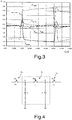
- Figure 3 shows the values of some voltages internal to the charge pump circuit 1 during the half-period in which charge sharing takes place between the pump capacitors C d , adjacent to one another, connected to the second internal nodes D i-1 , D i .
- the voltages at the control nodes P gD , N gD remain substantially constant during the entire half-period (for example, they do not have a variation of more than 4-6 %).
- the charge pump circuit 1 of Figure 2 has several advantages, and in particular enables, using only low voltage transistors, operation at high frequency (for example up to 150 MHz) with good electrical performance.
- the charge pump circuit is in general sized at the minimum supply voltage; it follows that the problem highlighted previously is particularly felt.
- the aim of the present invention is hence to provide a charge pump circuit that will enable, at least in part, solution of the problems highlighted previously, in particular as regards the requirements of current consumption and area occupation.
- a charge pump circuit is provided, as defined in the annexed claims.
- the present invention stems from the realization, by the present applicant, that the applications where charge pump circuits are employed usually have, in addition to the logic supply voltage Vdd, also an external supply voltage, having a decidedly wider range of values.
- an external supply voltage Vcc is available, for example with values between 1.65 V and 5.5 V.
- the present invention hence provides a solution for supplying a charge pump circuit having only low voltage transistors (for example, the circuit of Figure 2 ) with a power supply higher than the logic supply voltage Vdd, without the risk of damaging or even destroying the circuit, and in particular the oxides of the low voltage transistors.
- the first step is to assess the differences of potential between the various nodes internal to the charge pump circuit (for example, the circuit of Figure 2 ), considering, for simplicity, a single stage S i , which is shown in an extremely simplified way in Figure 4 .
- Figure 4 shows two pump capacitors C (which receive the low voltage phase signals FN and FX), for example coinciding with the pump capacitors C d of the bottom branch of the charge pump circuit, and two terminals, input A and output B, of the stage S i , for example coinciding with the terminals D i-1 and D i of the same bottom branch of the charge pump circuit.
- Figure 4 also represents as a whole with a single switch Ii the various pass transistors of the stage S i (and a similar representation is made for the switches I i-1 and I i+1 of the previous stage S i-1 and subsequent stage S i+1 ).
- the aforesaid Figure 4 refers in particular to a first operating condition, coinciding with end of charge sharing (the so-called “End Sharing", i.e., end of transfer of charge from one stage to the next), in which the CMOS switches of the stage S i and of the previous and subsequent stages are open.
- End Sharing end of charge sharing
- V AB Start_Sh 2 ⁇ ⁇ v
- V AB End_NoSh 2 ⁇ Vdd - 2 ⁇ ⁇ v
- the result is that the difference of potential between the source and drain terminals of the latch transistors M pD and M nD is at most equal to Vdd (hence not causing damage to the low voltage transistors).
- An aspect of the present invention consequently envisages modifying the charge pump circuit (in particular, the charge pump circuit 1 illustrated in Figure 2 , of the two-phase latch type), introducing an appropriate protection stage, having the function of protecting the latch transistors from overvoltages.
- a further aspect of the present invention envisages in fact supplying the charge pump circuit with a supply voltage of a value higher than the logic supply voltage Vdd (the latter being the maximum voltage sustainable by low voltage latch transistors).
- a charge pump circuit here designated by 10 (and illustrated in a schematic and simplified way), has a structure substantially similar to that of the circuit of a two-phase latch type shown in Figure 2 , and in particular has a plurality of charge pump stages S 1 , ..., S N , each of which comprises a first pump capacitor C u , connected to a first internal node U i (considering the generic i-th stage), associated to a top branch of the circuit, and a second pump capacitor C d , connected to a second internal node D i , associated to a bottom branch of the circuit (the two, top and bottom, branches being involved in alternating half-periods by the transfer of charge between the corresponding pump capacitors).
- Each charge pump stage S 1 , ..., S N further comprises a respective latch circuit L 1 , ..., L N , provided with latch transistors, appropriately controlled so as to enable transfer of charge from one stage to the next, and in particular between the first pump capacitors C u of the top branch, in a first operating half-period (referring to a clock signal), and between the second pump capacitors C d of the bottom branch, in the second operating half-period of the clock signal.
- Figure 5 shows only the latch transistors that enable transfer of charge from the charge pump stage S i-1 to the next charge pump stage S i , and in particular the first latch transistor M pU , of a low voltage PMOS type, the second latch transistor M pD , which is also of a low voltage PMOS type, the third latch transistor M nU , of a low voltage NMOS type, and the fourth latch transistor M nD , which is also of a low voltage NMOS type.
- the charge pump circuit 10 further comprises (in a way substantially similar to what has been described with reference to Figure 2 ) a stabilization stage, designated once again by 2, which is set between each consecutive pair of charge pump stages S i-1 , S i , and generates appropriate control signals for the gate terminals of the transistors of the latch circuits L i-1 , L i .
- the stabilization stage 2 receives at input the voltage V int present on the intermediate node INT between the charge pump stages S i-1 , S i , and the low voltage phase signals FX, FN (operating in the low voltage range, or logic voltage, comprised between 0 V, or ground, and Vdd, for example with values in the range between 1 V and 1.35 V), and supplies at output to the first and second control nodes P gU , P gD the control signals for biasing the gate terminals of the latch transistors M pU and M pD , and to the third and fourth control nodes N gU , N gD the control signals for biasing the gate terminals of the latch transistors M nU and M nD .
- the charge pump circuit 10 is supplied with a high supply voltage VddH, higher than the logic supply voltage Vdd, for example comprised between 1.65 V and 5.5 V.
- high voltage phase signals FXH, FNH (operating in the high voltage range comprised between 0 V, or ground, and the high supply voltage VddH) are supplied to the pump capacitors C u , C d (in a way alternating in the various successive stages, as indicated previously).
- the high voltage phase signals FXH, FNH have a high or low value corresponding to that of the low voltage phase signals FX, FN, given that they are shifted towards high voltage values with respect to the latter.
- the charge pump circuit 10 comprises, for each charge pump stage S i , a protection stage 12, set between the internal nodes U i , D i and the latch transistors M pU , M nU , M pD , M nD coupled to the same internal nodes U i , D i in such a way as to protect the latch transistors from overvoltages (in particular, deriving from use of the high supply voltage VddH, which, as highlighted previously, would otherwise fall entirely on the oxides of the same latch transistors).
- each protection stage 12 comprises protection transistors, connected between a respective internal node U i , D i and a respective latch transistor M pU , M nU , M pD , M nD , in a so-called "cascode" configuration (i.e., cascaded and traversed, in use, by the same current).
- Figure 6 (which once again refers only to the portion of the charge pump circuit 10 for transfer of charge between the charge pump stage S i-1 and the subsequent stage S i ) shows: a first protection transistor M cpU , of a low voltage PMOS type, which is connected between the first internal node U i-1 of the charge pump stage S i-1 and a node B, to which the first latch transistor M pU (operating once again as pass transistor) is also connected; a second protection transistor M cpD , of a low voltage PMOS type, which is connected between the second internal node D i-1 of the charge pump stage S i-1 and a node A, to which the second latch transistor M pD is also connected; a third protection transistor M cnU , of a low voltage NMOS type, which is connected between the first internal node U i of the charge pump stage S i and a node D, to which the third latch transistor M nU is also connected; and a fourth protection transistor M cn
- the gate terminals (or control terminals) of the first and second protection transistors M cpU , M cpD (having the same type of channel p), are connected together and are moreover connected to a first gate-biasing unit 14a of the protection stage 12, which supplies a first biasing voltage V cp , of an appropriate value.
- the gate terminals (or control terminals) of the third and fourth protection transistors M cnU , M cnD (having the same type of channel n), are connected together and are moreover connected to a second gate-biasing unit 14b of the protection stage 12, which supplies a second biasing voltage V cn , of an appropriate value.
- the first gate-biasing unit 14a has moreover inputs connected to the first and second control nodes P gU , P gD , whilst the second gate-biasing unit 14b has inputs connected to the third and fourth control nodes N gU , N gD .
- the protection stage 12 is configured so as to generate the first biasing voltage V cp of a constant value (during the entire period of the clock signal), equal to the minimum voltage that can be assumed by the first and second control nodes P gU , P gD , which is in particular equal to (V int - Vdd), and is moreover configured so as to assign to the second biasing voltage V cn a constant value equal to the maximum voltage that can be assumed by the third and fourth control nodes N gU , N gD , which is equal to (V int + Vdd).
- this choice of the values of the biasing voltages enables effective switching-on/switching-off of the protection transistors (of a PMOS and NMOS type), i.e., issuing of a command to the transistors for complete switching-on/complete switching-off.
- the protection stage 12 further comprises a well-biasing unit 15, of a known type that is not described in detail, designed to bias at the same biasing voltage the well terminals of the protection and latch PMOS transistors, coupled to one another (and to the first internal node U i and to the second internal node D i ).
- the well terminals of the protection and latch transistors of an NMOS type are, instead, connected to one another by an electrical connection line.
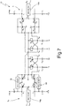
- Figure 7 shows in greater detail the circuit configuration of the charge pump stages S i-1 , S i and of the protection stage 12 (as it has already been described in detail with reference to Figure 2 ).
- the charge pump circuit 10 hence works with two different supply voltages (and respective pairs of phase signals): the voltage VddH for supplying the high voltage phase signals FHX and FHN; and the voltage Vdd for supplying the low voltage phase signals FX and FN.
- the circuit is examined once again during this operating step (for example, considering the charge sharing between the capacitors C d of the bottom branch of the circuit). Since the high voltage phase signals FXH and FNH are supplied with the voltage VddH, the maximum difference of potential between the nodes D i and D i-1 is now equal to 2VddH, as may be readily appreciated.
- the condition to be imposed is that the voltage drop across the gate and drain terminals should be lower than Vdd (it is recalled that all the transistors are in fact low voltage transistors; namely, they are able to withstand, without breakdown, voltages not higher than the logic supply voltage Vdd); it follows that the following relation is to be verified: V cp - V ⁇ D i - 1 ⁇ Vdd and accordingly: V int - Vdd - V int - VddH ⁇ Vdd
- VddH the maximum voltage that can be assigned to the high supply voltage VddH is equal to 2Vdd (in other words, the relation VddH ⁇ 2Vdd must be satisfied).
- V D i - V cn ⁇ Vdd the condition that the voltage drop across the gate and drain terminals should be lower than Vdd leads to the following relation: V D i - V cn ⁇ Vdd and accordingly: V int + VddH - V int + Vdd ⁇ Vdd
- the high supply voltage VddH has not to be higher than 2Vdd (VddH ⁇ 2Vdd).
- VddH is equal to 2Vdd min (where Vdd min is the minimum value that can be assumed, during operation of the charge pump circuit 10, by the logic supply voltage Vdd, taking into account, for example, its possible fluctuations), it is possible to operate always in safety conditions.
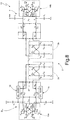
- Figure 8 shows the overall diagram of the charge pump circuit 10 (once again with reference to just the portions envisaged for transfer of charge from one stage S i-1 to the next stage S i ), showing in particular a possible circuit implementation of the gate-biasing units 14a, 14b of the protection stage 12.
- the first gate-biasing unit 14a comprises: a first buffer capacitor C b , which receives on a first terminal the first low voltage phase signal FX and has the second terminal connected to a node 16, internal to the first gate-biasing unit 14a; and a second buffer capacitor C b , which receives on a first terminal the second low voltage phase signal FN and has the second terminal connected to a node 18, internal to the first gate-biasing unit 14a.
- the first gate-biasing unit 14a further comprises: a first biasing transistor M bn1 , of a low voltage NMOS type, which has a first current-conduction terminal connected to the first control node P gU and a second current-conduction terminal connected to a biasing output of the first gate-biasing unit 14, present on which is the first biasing voltage V cp , and has its control terminal (or gate terminal) connected to the node 16; a second biasing transistor M bn2 , of a low voltage NMOS type, which is connected between the node 16 and the biasing output and has its control terminal (or gate terminal) connected to the node 18; a third biasing transistor M bn3 , of a low voltage NMOS type, which is connected between the node 18 and the biasing output and has its control terminal (or gate terminal) connected to the node 16 (the second and third biasing transistors M bn2 , M bn3 are hence connected in latch configuration); and a fourth biasing
- Operation of the first biasing unit 14a is such that the first biasing voltage V cp present on the biasing output is constant throughout the operating period of the charge pump circuit 10 and equal to the minimum voltage present on the control nodes P gU and P gD .
- the first biasing voltage V cp is therefore constantly equal to the expression V int - Vdd, for the entire period of operation of the charge pump circuit 10.
- the second gate-biasing unit 14b comprises: a respective first buffer capacitor C b , which receives on a first terminal the first low voltage phase signal FN and has the second terminal connected to a node 19, internal to the second gate-biasing unit 14b; and a respective second buffer capacitor C b , which receives on a first terminal the second low voltage phase signal FX and has the second terminal connected to a node 20, internal to the second gate-biasing unit 14b.
- the second gate-biasing unit 14b further comprises: a respective first biasing transistor M bp1 , of a low voltage PMOS type, which has a first current-conduction terminal connected to the third control node N gU and a second current-conduction terminal connected to a biasing output of the second gate-biasing unit 14b, present on which is the second biasing voltage V cn , and has its control terminal (or gate terminal) connected to the node 19; a respective second biasing transistor M bp2 , of a low voltage PMOS type, which is connected between the node 19 and the biasing output and has its control terminal (or gate terminal) connected to the node 20; a respective third biasing transistor M bp3 , of a low voltage PMOS type, which is connected between the node 20 and the biasing output and has its control terminal (or gate terminal) connected to the node 19 (the second and third biasing transistors M bp2 , M bp3 are hence connected in latch configuration); and a fourth
- Operation of the second biasing unit 14b is such that the second biasing voltage V cn present on the biasing output is constant during the entire period, and equal to the maximum voltage present on the control nodes N gU and N gD .
- the second biasing voltage V cn is hence constantly equal to the expression V int +Vdd for the entire period of operation of the charge pump circuit 10.
- the circuit configuration of the biasing units 14a, 14b is such as to exploit the same low voltage phase signals FX, FN being sent to the protection stage 12 in order to control opening and closing of the biasing transistors (M bn1 , M bn4 , M bp1 , M bp4 ) and consequent transfer at the output of the lowest/highest of the signals present on the control nodes P gD , P gU or N gD , N gU (in particular, the lowest of the signals present on the control nodes P gD , P gU , as regards the first biasing unit 14a, and the highest of the signals present on the control nodes N gD , N gU , as regards the second biasing unit 14b).
- the further biasing transistors (M bn2 , M bn3 , M bp2 , M bp3 ) are exploited to connect alternately the biasing capacitors C b to the output of the biasing units 14a, 14b so as to recover the charge lost in the previous half-period for driving the biasing transistors (M bn1 , M bn4 , M bp1 , M bp4 ).
- the nodes 16, 18, 19 and 20 are hence always at voltage values such as to open/close in an effective and complete way the transistors the gate terminals of which are connected thereto.
- a high voltage on the node 16 of the first biasing unit 14a enables at the same time closing of the biasing transistors M bn1 and M bn3 , and hence both the transfer of the signal present on the control node P gU to the output and refresh at the same output voltage of the biasing capacitor C b belonging to the other node 18; instead, the biasing transistors M bn2 and M bn4 in the same half-period are open, given the complementary values of the low voltage phase signals FX, FN.
- the charge pump circuit 10 can be advantageously used in a memory device 30, for example of a CMOS flash type, comprising an array 31 of memory cells 32.
- the memory cells 32 have their gate terminal connected to a respective wordline WL and their drain terminal connected to a respective bitline BL.
- the charge pump circuit 10 is connected to the drain terminals of the memory cells 32, through interposition of a column decoder 35.
- the load of the charge pump circuit 10 is in this case basically constituted by the capacitance of the bitlines BL of the memory array 31.
- the charge pump circuit 10 is in this case used for generating the high programming (writing/erasure) and reading voltages required for the memory cells 32.
- the charge pump circuit finds advantageous, though not exclusive, application within a memory device, for generating the high voltages required for the programming and reading operations; other uses can be equally envisaged, in all those cases where it is necessary to generate a boosted voltage starting from a lower voltage value.
- circuit modifications may be envisaged, which do not alter the general operating principle of the circuit.
- the gate-biasing units 14a, 14b in the protection stage 12 may have a different configuration, which will enable in any case generation of the desired values for the biasing voltages V cp and V cn .
Landscapes
- Engineering & Computer Science (AREA)
- Power Engineering (AREA)
- Dc-Dc Converters (AREA)
- Semiconductor Integrated Circuits (AREA)
- Dram (AREA)
Abstract
Description
- The present invention regards a charge pump circuit using low voltage transistors.
- As is known, charge pump circuits are widely used in a wide range of electronic applications in order to obtain output voltage values higher than a given input voltage (basically operating as DC-DC boost converters), exploiting the use of capacitors as charge-accumulation elements.
- For example, charge pump circuits are used in flash-memory devices for generating the high voltage values required for performing data reading, writing, and erasing operations, starting from the low values of the internal supply voltage (the so-called "logic supply voltage Vdd", with values, for example, comprised between 1 V and 1.35 V, for CMOS flash-memory devices in 90-nm technology).
- In particular, charge pump circuits of a latch type (also known as "latch circuits") have been proposed, operating with just two enabling signals (or phase signals) and using only low voltage transistors (having, for example, a maximum sustainable voltage comprised between 1 V and 1.35 V). These circuits are thus able to operate at high frequencies, for example of the order of 100 MHz (unlike common four-phase charge pump circuits, capable of reaching at most frequencies of 10-50 MHz).
- In brief, and as shown in
Figure 1 , a two-phase charge pump latch circuit, designated as a whole by 1, has an input terminal IN, on which it receives the logic supply voltage Vdd (in particular, a supply voltage with logic values), and an output terminal OUT, on which it supplies the boosted output voltage Vout, for a load (schematically represented as the parallel connection of a load capacitor CL and a current generator IL). - The
charge pump circuit 1 comprises a plurality N of stages S1, ..., SN, cascaded between the input terminal IN and the output terminal OUT, each receiving a first low voltage phase signal FX and a second low voltage phase signal FN, having negated (or complementary) values with respect to one another. An intermediate node INT is present between two successive stages in the charge pump circuit 1 (the intermediate node INT hence corresponding to the output of the previous charge pump stage Si-1, and to the input of the next stage Si). The low voltage phase signals FX, FN have, for example, logic values equal to 0 (or ground, GND) or to Vdd, and are generated by an appropriate generator circuit (not illustrated). - Each stage S1, ..., SN comprises a first pump capacitor Cu and a second pump capacitor Cd, receiving the first low voltage phase signal FX or the second low voltage phase signal FN (it should be noted that the arrangement of the phase signals is reversed from one stage to the next; i.e., if the first pump capacitor Cu of a given stage receives the first low voltage phase signal FX, the corresponding first pump capacitor Cu of the immediately preceding stage and immediately subsequent stage receives the second low voltage phase signal FN). The first and second pump capacitors Cu, Cd are moreover connected, respectively, to a first internal node U1, ..., UN and to a second internal node D1, ..., DN.
- Each stage S1, ..., SN further comprises a latch circuit L1, ..., LN, comprising a pair of NMOS latch transistors (of a low voltage type) and a pair of PMOS latch transistors (which are also of a low voltage type), the control terminals of which are appropriately connected to the internal nodes U1, ..., UN, D1, ..., DN, so as to provide switches designed to enable selective and alternate transfer of the charge accumulated in the pump capacitors Cu, Cd from one stage to the next (these transistors are for this reason commonly referred to as "pass transistors").
- In particular, it may readily be appreciated that the arrangement of the transistors in the latch circuits L1, ..., LN is such as to perform transfer of charge between the first pump capacitors Cu of successive stages, in a first half-period (in which the first low voltage phase signal FX is high, for example equal to Vdd, and the second low voltage phase signal FN is low, for example equal to 0 V), and to perform transfer of charge between the second pump capacitors Cd of successive stages, in a second half-period (in which the first low voltage phase signal FX is low and the second low voltage phase signal FN is high), thus guaranteeing the voltage-boost effect between the input terminal IN and the output terminal OUT. The first and second half-periods refer, for example, to a common periodic synchronisation signal (or clock signal).
- Moreover, it may be appreciated that the voltage on the intermediate node INT remains practically constant during the entire operating period of the charge pump circuit.
- In order to improve the performance of the aforesaid charge pump circuit of a latch type, in particular in operating conditions with very low values of the supply voltage (i.e., for limit values lower than the logic supply voltage Vdd, for example, 1 V), in patent application No.
EP-A-1 881 589 an improved circuit has been proposed, as shown inFigure 2 (which, for simplicity of illustration, refers to a single pair of consecutive stages Si-1, Si of the charge pump circuit, which is once again designated by the reference number 1). - In detail, each charge pump stage Si-1, Si comprises once again a first pump capacitor Cu and a second pump capacitor Cd, receiving respective low voltage phase signals FX, FN, complementary to one another, and are connected to a respective internal node Ui-1, Ui and Di-1, Di.
- Each charge pump stage Si-1, Si further comprises a latch circuit Li-1, Li with suitable transistors operating as switches (or pass transistors). For simplicity of illustration, only the transistors involved in the transfer of charge between the charge pump stages Si-1, Si, in particular between the respective first pump capacitors Cu or second pump capacitors Cd are represented in
Figure 2 (it being altogether evident that similar transistors are, however, present for transfer of charge with respect to the immediately preceding and subsequent stages). - In particular, a first latch transistor MpU, of a low voltage PMOS type (here shown only in the charge pump stage Si-1) is connected between the internal node Ui-1 and an intermediate node INT (set between the consecutive charge pump stages Si-1 and Si), and has a gate terminal connected to a first control node PgU; a second latch transistor MpD, of a low voltage PMOS type (in the same charge pump stage Si-1) is connected between the internal node Di-1 and the intermediate node INT, and has a gate terminal connected to a second control node PgD; a third latch transistor MnU, of a low voltage NMOS type (herein shown only in the charge pump stage Si) is connected between the internal node Ui and the intermediate node INT, and has a gate terminal connected to a third control node NgU; and a fourth latch transistor MnD, of a low voltage NMOS type (in the same stage Si of the charge pump circuit 1) is connected between the internal node Di and the intermediate node INT, and has a gate terminal connected to a fourth control node NgD.
- It should be noted that, for the purposes of operation of the charge pump circuit, the distinction between the drain and source terminals of the various MOS transistors is not important so that they can be referred to generically as "current-conduction terminals". Moreover, as highlighted previously, it is evident that each latch circuit Li-1, Li further comprises latch transistors for charge sharing with the adjacent stages. For example, the latch circuit Li further comprises, downstream of the internal node Ui PMOS latch transistors altogether similar to the first and second latch transistors MpU, MpD.
- The
charge pump circuit 1 further comprises astabilization stage 2, which is set between each consecutive pair of charge pump stages Si-1, Si, and generates appropriate control signals for the gate terminals of the transistors of the latch circuits Li-1, Li. - The
stabilization stage 2 comprises: afirst biasing unit 2a for biasing the gate terminals of the latch transistors MpU and MpD of the charge pump stage Si-1; and asecond biasing unit 2b for biasing the gate terminals of the latch transistors MnU and MnD of the charge pump stage Si. - In detail, the
first biasing unit 2a comprises: a first biasing capacitor Cb1, having a first terminal receiving the low voltage phase signal FX and a second terminal connected to the second control node PgD; a second biasing capacitor Cb2, having a first terminal receiving the low voltage phase signal FN and a second terminal connected to the first control node PgU; a first control transistor Mp1, of a low voltage PMOS type, which is connected between the intermediate terminal INT and the second control node PgD, and has its gate terminal connected to the first control node PgU; and a second control transistor Mp2, of a low voltage PMOS type, which is connected between the intermediate terminal INT and the first control node PgU, and has its gate terminal connected to the second control node PgD. - Likewise, the
second biasing unit 2b comprises: a third biasing capacitor Cb3, having a first terminal receiving the low voltage phase signal FX and a second terminal connected to the third control node NgU; a fourth biasing capacitor Cb4, having a first terminal receiving the low voltage phase signal FN and a second terminal connected to the fourth control node NgD; a third control transistor Mn1, of a low voltage NMOS type, which is connected between the intermediate terminal INT and the third control node NgU, and has its gate terminal connected to the fourth control node NgD; and a fourth control transistor Mn2, of a low voltage NMOS type, which is connected between the intermediate terminal INT and the fourth control node NgD, and has its gate terminal connected to the third control node NgU. - In general, the pump capacitors Cu, Cd may have a same first nominal capacitance; likewise, the first, second, third, and fourth biasing capacitors Cb1, Cb2, Cb3 and Cb4 may have a same second nominal capacitance.
- The voltage Vint on the intermediate node INT, which remains substantially constant for the entire operating period, is used by the
biasing stage 2 for correctly driving switching-on and switching-off of the pass transistors in the latch circuits Li-1, Li. - In detail, it is possible to distinguish the two following operating conditions, equivalent to one another, respectively in a first half-period and in a second half-period of the clock signal:
- FN = Vdd, FX = 0: V(Di-1) (it should be noted that V(D) and V(U) are the voltages at the corresponding nodes D and U) goes to a high value and V(Ui-1) goes to a low value; likewise V(Di) is at a low value, whilst V(Ui) is at a high value; in this case, the first control node PgU goes to a high value (equal to Vint), whereas the second control node PgD goes to a low value (in particular, it decreases by a value equal to the logic supply voltage Vdd with respect to Vint), thus enabling switching-on of the second latch transistor MpD and switching-off of the first latch transistor MpU; in the same half-period, the fourth control node NgD goes to a high value (higher by a value equal to the supply voltage Vdd with respect to Vint), and the third control node NgU goes to a low value; consequently, the fourth latch transistor MnD switches on, whereas the third latch transistor MnU switches off; in this way, charge sharing is obtained between the two pump capacitors Cd, adjacent to one another, connected to the second internal nodes Di-1. Di. whereas charge sharing between the two pump capacitors Cu, connected to the first internal nodes Ui-1, Ui is prevented (note that by "charge sharing" is meant a transfer of charge from the previous stage to the next);
- FN = 0, FX = Vdd: in this case, the circuit operates in a way altogether similar to the previous situation, with the difference that charge sharing occurs between the two pump capacitors Cu connected to the first internal nodes Ui-1, Ui (in other words, charge transfer involves the top branch of the circuit).
- Advantageously, during the two half-periods in which the control nodes PgD, PgU, NgD, NgU go to a high or a low level, the same control nodes remain, throughout charge sharing, always at a substantially constant voltage, of a value such as to enable an effective switching-on, or switching-off, of the latch transistors connected thereto (in other words, any fluctuation in the logic supply voltage Vdd is prevented from possibly jeopardising switching-on/switching-off of the transistors). The control transistors Mp1, Mp2, Mn1, Mn2 enable the capacitances of the biasing capacitors Cb1, Cb2, Cb3, Cb4 to be updated to the voltage of the nodes to which they refer and to recover the charge lost for driving the respective latch transistors. The biasing capacitors hence act as "bootstrap" capacitors, effectively driving the gate terminals of the latch transistors.
- In particular, even in the case where the logic supply voltage Vdd is particularly low, for example equal to 1 V, the
charge pump circuit 1 continues to operate properly, unlike, for example, the circuit ofFigure 1 , where instead, the internal nodes Di, Ui may vary their voltage value during the various half-periods (being directly connected to a pump capacitor), up to possibly preventing the corresponding pass transistors from switching on. -
Figure 3 shows the values of some voltages internal to thecharge pump circuit 1 during the half-period in which charge sharing takes place between the pump capacitors Cd, adjacent to one another, connected to the second internal nodes Di-1, Di. In particular, it may be noted that the voltages at the control nodes PgD, NgD remain substantially constant during the entire half-period (for example, they do not have a variation of more than 4-6 %). - The
charge pump circuit 1 ofFigure 2 has several advantages, and in particular enables, using only low voltage transistors, operation at high frequency (for example up to 150 MHz) with good electrical performance. - However, the same circuit has a drawback, principally linked to the area occupation (in the integrated implementation on silicon) and to the current consumption.
- In this regard, it should be noted that the "pumping" capacitance of the
charge pump circuit 1 is given by the following expression:
where N is the number of stages of the pump; IL is the current supplied to the load; Vdd is the logic supply voltage (for example, the internal supply voltage of the memory in which thecharge pump circuit 1 is used); Vout is the output voltage of thecharge pump circuit 1; and f is the clock frequency (which determines the periodicity of operation of the circuit). - Moreover, the current consumption of the
charge pump circuit 1, i.e., the current required by the power supply (which supplies the voltage Vdd) is given by the following expression:
where α is the ratio between the value of the parasitic capacitance of the circuit and the value of the pumping capacitance defined previously. - It may thus be appreciated that, if supply voltages of a low value (for example, 1 V) are used for operation, then the need arises to have higher pumping capacitances and a greater number of stages in the charge pump circuit in order to reach desired values for the output voltage and the current supplied to the load; in turn, this involves a larger area occupation and a higher current consumption.
- It should be noted that, given that it is necessary in all cases to satisfy the specifications of current required by the load, the charge pump circuit is in general sized at the minimum supply voltage; it follows that the problem highlighted previously is particularly felt.
- The aim of the present invention is hence to provide a charge pump circuit that will enable, at least in part, solution of the problems highlighted previously, in particular as regards the requirements of current consumption and area occupation.
- According to the present invention, a charge pump circuit is provided, as defined in the annexed claims.
- For a better understanding of the present invention, preferred embodiments thereof are now described, purely by way of nonlimiting example, with reference to the attached drawings, wherein:
-
Figure 1 is a schematic illustration of a first charge pump circuit of a known type; -
Figure 2 is a schematic illustration of a second charge pump circuit of a known type; -
Figure 3 shows the plot of signals within the circuit ofFigure 2 ; -
Figure 4 shows a functional diagram of the circuit ofFigure 2 ; -
Figure 5 is a schematic illustration of a charge pump circuit, according to one embodiment of the present invention; -
Figures 6-8 show, with increasing level of detail, a circuit embodiment of the circuit ofFigure 5 ; and -
Figure 9 shows a block diagram of a storage device incorporating the circuit ofFigure 5 . - The present invention stems from the realization, by the present applicant, that the applications where charge pump circuits are employed usually have, in addition to the logic supply voltage Vdd, also an external supply voltage, having a decidedly wider range of values. For example, in the case of use in flash-memory devices, an external supply voltage Vcc is available, for example with values between 1.65 V and 5.5 V. The present invention hence provides a solution for supplying a charge pump circuit having only low voltage transistors (for example, the circuit of
Figure 2 ) with a power supply higher than the logic supply voltage Vdd, without the risk of damaging or even destroying the circuit, and in particular the oxides of the low voltage transistors. The present applicant has, in fact, noted that the use of a higher supply voltage would enable reduction of the area occupation and of the current consumption, at the same time safeguarding the advantages of simplicity of construction and of high operating frequency linked to charge pump circuits of a two-phase latch type, which use only low voltage transistors. - In order to determine a maximum applicable voltage value, the first step is to assess the differences of potential between the various nodes internal to the charge pump circuit (for example, the circuit of
Figure 2 ), considering, for simplicity, a single stage Si, which is shown in an extremely simplified way inFigure 4 . - In particular,
Figure 4 shows two pump capacitors C (which receive the low voltage phase signals FN and FX), for example coinciding with the pump capacitors Cd of the bottom branch of the charge pump circuit, and two terminals, input A and output B, of the stage Si, for example coinciding with the terminals Di-1 and Di of the same bottom branch of the charge pump circuit. Moreover,Figure 4 also represents as a whole with a single switch Ii the various pass transistors of the stage Si (and a similar representation is made for the switches Ii-1 and Ii+1 of the previous stage Si-1 and subsequent stage Si+1). - The aforesaid
Figure 4 refers in particular to a first operating condition, coinciding with end of charge sharing (the so-called "End Sharing", i.e., end of transfer of charge from one stage to the next), in which the CMOS switches of the stage Si and of the previous and subsequent stages are open. In this operating condition, intuitively, the difference of potential between the terminals A and B is zero:
- During charge sharing, the voltage at the input terminal A drops by an amount ΔV

where IL is the current supplied to the load, C is the capacitance of the pump capacitors, and T is the period of the clock signal. - During charge sharing, moreover, the voltage at the output terminal B increases by the same amount ΔV; it follows that, at the start of charge sharing, the following expression applies:

- Starting from the instant of end of charge sharing (or of start of the subsequent step of no charge sharing), the low voltage phase signals FX and FN switch, and consequently the voltage at the input terminal A drops by an amount equal to the supply voltage Vdd, whereas the voltage at the output terminal B increases by the same amount. The following expression hence applies:

- In this time interval, there is no charge sharing in the stage Si (as regards, for example, the bottom branch of the circuit), whereas there is charge sharing in the adjacent stages Si-1 and Si+1. Consequently, the pump capacitor connected to the input terminal A receives charge from the previous stage Si-1, and the pump capacitor connected to the output terminal B yields charge to the subsequent stage Si+1.
- At the end of the time interval of no charge sharing, the voltage at the input terminal A has hence increased by ΔV, whereas the voltage at the output terminal B has dropped by ΔV. Consequently,

- From the above considerations, it follows that the maximum difference of potential between the nodes internal to the charge pump circuit takes place at start of the time interval of no charge sharing ("Start No Sharing"), and is equal to 2·Vdd (i.e., to twice the logic supply voltage Vdd).
- Applying now these considerations to the
charge pump circuit 1 ofFigure 2 (see also the previous discussion), it follows that the maximum difference of potential takes place between the internal nodes Di-1 and Di. In particular, during the aforesaid time interval (of very short duration) of start of the step of no charge sharing, the latch transistors MpD and MnD are both open (or off), whereas the latch transistors MpU and MnU are both closed (or on). The latter hence maintain the intermediate node INT at an intermediate voltage between the voltages present on the two internal nodes Ui-1 and Ui. - Consequently, the result is that the difference of potential between the source and drain terminals of the latch transistors MpD and MnD is at most equal to Vdd (hence not causing damage to the low voltage transistors).
- As may be readily understood, if the supply voltage used for the charge pump circuit (in particular for defining the dynamics of the low voltage phase signals FX, FN) were higher than Vdd, the effect of this voltage would fall entirely on the oxides of the latch transistors MpD and MnD, jeopardizing operation of the same transistors up to their possible destruction.
- Similar considerations apply to the latch transistors MpU and MnU, during the step of start of no charge sharing between the capacitors CU of the top branch of the
charge pump circuit 1. - An aspect of the present invention consequently envisages modifying the charge pump circuit (in particular, the
charge pump circuit 1 illustrated inFigure 2 , of the two-phase latch type), introducing an appropriate protection stage, having the function of protecting the latch transistors from overvoltages. A further aspect of the present invention envisages in fact supplying the charge pump circuit with a supply voltage of a value higher than the logic supply voltage Vdd (the latter being the maximum voltage sustainable by low voltage latch transistors). - In detail, as initially shown in
Figure 5 , a charge pump circuit, here designated by 10 (and illustrated in a schematic and simplified way), has a structure substantially similar to that of the circuit of a two-phase latch type shown inFigure 2 , and in particular has a plurality of charge pump stages S1, ..., SN, each of which comprises a first pump capacitor Cu, connected to a first internal node Ui (considering the generic i-th stage), associated to a top branch of the circuit, and a second pump capacitor Cd, connected to a second internal node Di, associated to a bottom branch of the circuit (the two, top and bottom, branches being involved in alternating half-periods by the transfer of charge between the corresponding pump capacitors). - Each charge pump stage S1, ..., SN further comprises a respective latch circuit L1, ..., LN, provided with latch transistors, appropriately controlled so as to enable transfer of charge from one stage to the next, and in particular between the first pump capacitors Cu of the top branch, in a first operating half-period (referring to a clock signal), and between the second pump capacitors Cd of the bottom branch, in the second operating half-period of the clock signal. By way of example (in a way similar to what is illustrated in
Figure 2 ),Figure 5 shows only the latch transistors that enable transfer of charge from the charge pump stage Si-1 to the next charge pump stage Si, and in particular the first latch transistor MpU, of a low voltage PMOS type, the second latch transistor MpD, which is also of a low voltage PMOS type, the third latch transistor MnU, of a low voltage NMOS type, and the fourth latch transistor MnD, which is also of a low voltage NMOS type. - The
charge pump circuit 10 further comprises (in a way substantially similar to what has been described with reference toFigure 2 ) a stabilization stage, designated once again by 2, which is set between each consecutive pair of charge pump stages Si-1, Si, and generates appropriate control signals for the gate terminals of the transistors of the latch circuits Li-1, Li. As shown schematically inFigure 5 , thestabilization stage 2 receives at input the voltage Vint present on the intermediate node INT between the charge pump stages Si-1, Si, and the low voltage phase signals FX, FN (operating in the low voltage range, or logic voltage, comprised between 0 V, or ground, and Vdd, for example with values in the range between 1 V and 1.35 V), and supplies at output to the first and second control nodes PgU, PgD the control signals for biasing the gate terminals of the latch transistors MpU and MpD, and to the third and fourth control nodes NgU, NgD the control signals for biasing the gate terminals of the latch transistors MnU and MnD. - According to one aspect of the invention, the
charge pump circuit 10 is supplied with a high supply voltage VddH, higher than the logic supply voltage Vdd, for example comprised between 1.65 V and 5.5 V. In particular, high voltage phase signals FXH, FNH (operating in the high voltage range comprised between 0 V, or ground, and the high supply voltage VddH) are supplied to the pump capacitors Cu, Cd (in a way alternating in the various successive stages, as indicated previously). The high voltage phase signals FXH, FNH have a high or low value corresponding to that of the low voltage phase signals FX, FN, given that they are shifted towards high voltage values with respect to the latter. - Moreover, the
charge pump circuit 10 comprises, for each charge pump stage Si, aprotection stage 12, set between the internal nodes Ui, Di and the latch transistors MpU, MnU, MpD, MnD coupled to the same internal nodes Ui, Di in such a way as to protect the latch transistors from overvoltages (in particular, deriving from use of the high supply voltage VddH, which, as highlighted previously, would otherwise fall entirely on the oxides of the same latch transistors). - In detail, and as shown in
Figure 6 , eachprotection stage 12 comprises protection transistors, connected between a respective internal node Ui, Di and a respective latch transistor MpU, MnU, MpD, MnD, in a so-called "cascode" configuration (i.e., cascaded and traversed, in use, by the same current). - In particular,
Figure 6 (which once again refers only to the portion of the charge pump circuit 10 for transfer of charge between the charge pump stage Si-1 and the subsequent stage Si) shows: a first protection transistor McpU, of a low voltage PMOS type, which is connected between the first internal node Ui-1 of the charge pump stage Si-1 and a node B, to which the first latch transistor MpU (operating once again as pass transistor) is also connected; a second protection transistor McpD, of a low voltage PMOS type, which is connected between the second internal node Di-1 of the charge pump stage Si-1 and a node A, to which the second latch transistor MpD is also connected; a third protection transistor McnU, of a low voltage NMOS type, which is connected between the first internal node Ui of the charge pump stage Si and a node D, to which the third latch transistor MnU is also connected; and a fourth protection transistor McnD, of a low voltage NMOS type, which is connected between the second internal node Di of the charge pump stage Si and a node C, to which the fourth latch transistor MnD is also connected (it should be noted that the protection transistors have the same type of channel, n or p, as that of the respective latch transistor to which they are connected in cascode configuration). - The gate terminals (or control terminals) of the first and second protection transistors McpU, McpD (having the same type of channel p), are connected together and are moreover connected to a first gate-biasing
unit 14a of theprotection stage 12, which supplies a first biasing voltage Vcp, of an appropriate value. Likewise, the gate terminals (or control terminals) of the third and fourth protection transistors McnU, McnD (having the same type of channel n), are connected together and are moreover connected to a second gate-biasingunit 14b of theprotection stage 12, which supplies a second biasing voltage Vcn, of an appropriate value. The first gate-biasingunit 14a has moreover inputs connected to the first and second control nodes PgU, PgD, whilst the second gate-biasingunit 14b has inputs connected to the third and fourth control nodes NgU, NgD. - In particular, as will be described in detail hereinafter, the
protection stage 12 is configured so as to generate the first biasing voltage Vcp of a constant value (during the entire period of the clock signal), equal to the minimum voltage that can be assumed by the first and second control nodes PgU, PgD, which is in particular equal to (Vint - Vdd), and is moreover configured so as to assign to the second biasing voltage Vcn a constant value equal to the maximum voltage that can be assumed by the third and fourth control nodes NgU, NgD, which is equal to (Vint + Vdd). - Intuitively, this choice of the values of the biasing voltages enables effective switching-on/switching-off of the protection transistors (of a PMOS and NMOS type), i.e., issuing of a command to the transistors for complete switching-on/complete switching-off.
- As shown in the same
Figure 6 , theprotection stage 12 further comprises a well-biasingunit 15, of a known type that is not described in detail, designed to bias at the same biasing voltage the well terminals of the protection and latch PMOS transistors, coupled to one another (and to the first internal node Ui and to the second internal node Di). The well terminals of the protection and latch transistors of an NMOS type are, instead, connected to one another by an electrical connection line. - Some considerations are now made on the maximum values of the voltages present within the
charge pump circuit 10, in particular in order to define the maximum value of the high supply voltage VddH, which can be used in the same circuit. - In particular, reference is here made to
Figure 7 , which shows in greater detail the circuit configuration of the charge pump stages Si-1, Si and of the protection stage 12 (as it has already been described in detail with reference toFigure 2 ). - It should be noted that the
charge pump circuit 10 hence works with two different supply voltages (and respective pairs of phase signals): the voltage VddH for supplying the high voltage phase signals FHX and FHN; and the voltage Vdd for supplying the low voltage phase signals FX and FN. - In particular, given that the maximum difference of potential between the internal nodes (for example, the nodes Di and Di-1) of the
charge pump circuit 10 takes place during the "Start No Sharing" step, the circuit is examined once again during this operating step (for example, considering the charge sharing between the capacitors Cd of the bottom branch of the circuit). Since the high voltage phase signals FXH and FNH are supplied with the voltage VddH, the maximum difference of potential between the nodes Di and Di-1 is now equal to 2VddH, as may be readily appreciated. - The voltages of the internal nodes of the bottom circuit branch during this operating step are summed up in the table below.
Table 1 V (D1-1) Vint-VddH Vcp Vint-Vdd V(A) Vint-Vdd+Vth V(PgD) Vint V(int) Vint V(NgD) Vint V(C) Vint+Vdd-Vth VCN Vint+Vdd V(D1) Vint+VddH - The maximum voltage drops take place on the protection transistors (in the case of the bottom branch, the second and fourth protection transistors McpD and McnD), which are hence critical. It is, instead, evident that in all the other cases the differences of potential are lower than Vdd so as not to create any risk of breakdown of the junction oxides.
- As regards the second protection transistor McpD, in order to prevent breakdown of the oxides, the condition to be imposed is that the voltage drop across the gate and drain terminals should be lower than Vdd (it is recalled that all the transistors are in fact low voltage transistors; namely, they are able to withstand, without breakdown, voltages not higher than the logic supply voltage Vdd); it follows that the following relation is to be verified:

and accordingly:
- It follows that the maximum voltage that can be assigned to the high supply voltage VddH is equal to 2Vdd (in other words, the relation VddH ≤ 2Vdd must be satisfied).
- Likewise, as regards the fourth protection transistor McnD, the condition that the voltage drop across the gate and drain terminals should be lower than Vdd leads to the following relation:

and accordingly:
- Also in this case, the high supply voltage VddH has not to be higher than 2Vdd (VddH ≤ 2Vdd).
- Therefore, imposing, for example, that the voltage VddH is equal to 2Vddmin (where Vddmin is the minimum value that can be assumed, during operation of the
charge pump circuit 10, by the logic supply voltage Vdd, taking into account, for example, its possible fluctuations), it is possible to operate always in safety conditions. -
Figure 8 shows the overall diagram of the charge pump circuit 10 (once again with reference to just the portions envisaged for transfer of charge from one stage Si-1 to the next stage Si), showing in particular a possible circuit implementation of the gate-biasingunits protection stage 12. - In detail, the first gate-biasing
unit 14a comprises: a first buffer capacitor Cb, which receives on a first terminal the first low voltage phase signal FX and has the second terminal connected to anode 16, internal to the first gate-biasingunit 14a; and a second buffer capacitor Cb, which receives on a first terminal the second low voltage phase signal FN and has the second terminal connected to anode 18, internal to the first gate-biasingunit 14a. - The first gate-biasing
unit 14a further comprises: a first biasing transistor Mbn1, of a low voltage NMOS type, which has a first current-conduction terminal connected to the first control node PgU and a second current-conduction terminal connected to a biasing output of the first gate-biasing unit 14, present on which is the first biasing voltage Vcp, and has its control terminal (or gate terminal) connected to thenode 16; a second biasing transistor Mbn2, of a low voltage NMOS type, which is connected between thenode 16 and the biasing output and has its control terminal (or gate terminal) connected to thenode 18; a third biasing transistor Mbn3, of a low voltage NMOS type, which is connected between thenode 18 and the biasing output and has its control terminal (or gate terminal) connected to the node 16 (the second and third biasing transistors Mbn2, Mbn3 are hence connected in latch configuration); and a fourth biasing transistor Mbn4, of a low voltage NMOS type, which has a first current-conduction terminal connected to the second control node PgD and a second current-conduction terminal connected to the biasing output, and has its control terminal (or gate terminal) connected to thenode 18. - Operation of the
first biasing unit 14a is such that the first biasing voltage Vcp present on the biasing output is constant throughout the operating period of thecharge pump circuit 10 and equal to the minimum voltage present on the control nodes PgU and PgD. - In detail, during a first half-period of charge sharing between the capacitors CU of the top branch of the circuit, the following conditions are verified (it should be noted that "ON" and "OFF" indicate, respectively, the condition of switching-on and the condition of switching-off of the transistors):
- FHN = Gnd ; FHX = VddH
- FN = Gnd ; FX = Vdd
- V(PgD) = Vint ; V(PgU) = Vint-Vdd
- Mp1 → ON ; Mp2 → OFF
- McpU → ON ; McpD → OFF
- Mbn2 → OFF ; Mbn4 → OFF
- Mbn3 → ON ; Mbn1 → ON
- Likewise, in a second half-period of charge sharing between the capacitors CD of the bottom branch of the circuit, the following respective conditions are verified:
- FHN = VddH ; FHX = Gnd
- FN = Vdd ; FX = Gnd
- V(PgD) = Vint -Vdd ; V(PgU) = Vint
- Mp1 → OFF ; Mp2 → ON
- McpU → OFF ; McpD → ON
- Mbn2 → ON ; Mbn4 → ON
- Mbn3 → OFF ; Mbn1 → OFF
- The first biasing voltage Vcp, as desired, is therefore constantly equal to the expression Vint - Vdd, for the entire period of operation of the
charge pump circuit 10. - In a substantially similar way, the second gate-biasing
unit 14b comprises: a respective first buffer capacitor Cb, which receives on a first terminal the first low voltage phase signal FN and has the second terminal connected to a node 19, internal to the second gate-biasingunit 14b; and a respective second buffer capacitor Cb, which receives on a first terminal the second low voltage phase signal FX and has the second terminal connected to a node 20, internal to the second gate-biasingunit 14b. - The second gate-biasing
unit 14b further comprises: a respective first biasing transistor Mbp1, of a low voltage PMOS type, which has a first current-conduction terminal connected to the third control node NgU and a second current-conduction terminal connected to a biasing output of the second gate-biasingunit 14b, present on which is the second biasing voltage Vcn, and has its control terminal (or gate terminal) connected to the node 19; a respective second biasing transistor Mbp2, of a low voltage PMOS type, which is connected between the node 19 and the biasing output and has its control terminal (or gate terminal) connected to the node 20; a respective third biasing transistor Mbp3, of a low voltage PMOS type, which is connected between the node 20 and the biasing output and has its control terminal (or gate terminal) connected to the node 19 (the second and third biasing transistors Mbp2, Mbp3 are hence connected in latch configuration); and a fourth biasing transistor Mbp4, of a low voltage PMOS type, which has a first current-conduction terminal connected to the fourth control node NgD and a second current-conduction terminal connected to the biasing output, and has its control terminal (or gate terminal) connected to the node 20. - Operation of the
second biasing unit 14b is such that the second biasing voltage Vcn present on the biasing output is constant during the entire period, and equal to the maximum voltage present on the control nodes NgU and NgD. - In detail, in a first half-period of charge sharing between the capacitors CU of the top branch of the circuit, the following conditions are valid:
- FHN = Gnd ; FHX = VddH
- FN = Gnd ; FX = Vdd
- V(NgD) = Vint ; V(NgU) = Vint -Vdd
- Mn1 → OFF ; Mn2 → ON
- McnU → ON ; McnD → OFF
- Mbp2 → OFF ; Mbp4 → OFF
- Mbp3 → ON ; Mbp1 → ON
- Likewise, in a second half-period of charge sharing between the capacitors CD of the bottom branch of the circuit, the following respective conditions are valid:
- FHN = VddH ; FHX = Gnd
- FN = Vdd ; FX = Gnd
- V(NgD) = Vint +Vdd ; V(NgU) = Vint
- Mn1 → OFF ; Mn2 → ON
- McnU → OFF ; McnD → ON
- Mbp2 → ON ; Mbp4 → ON
- Mbp3 → OFF ; Mbp1 → OFF
- The second biasing voltage Vcn, as desired, is hence constantly equal to the expression Vint+Vdd for the entire period of operation of the
charge pump circuit 10. - Basically, the circuit configuration of the biasing
units protection stage 12 in order to control opening and closing of the biasing transistors (Mbn1, Mbn4, Mbp1, Mbp4) and consequent transfer at the output of the lowest/highest of the signals present on the control nodes PgD, PgU or NgD, NgU (in particular, the lowest of the signals present on the control nodes PgD, PgU, as regards thefirst biasing unit 14a, and the highest of the signals present on the control nodes NgD, NgU, as regards thesecond biasing unit 14b). Moreover, the further biasing transistors (Mbn2, Mbn3, Mbp2, Mbp3) are exploited to connect alternately the biasing capacitors Cb to the output of the biasingunits nodes node 16 of thefirst biasing unit 14a enables at the same time closing of the biasing transistors Mbn1 and Mbn3, and hence both the transfer of the signal present on the control node PgU to the output and refresh at the same output voltage of the biasing capacitor Cb belonging to theother node 18; instead, the biasing transistors Mbn2 and Mbn4 in the same half-period are open, given the complementary values of the low voltage phase signals FX, FN. - As shown schematically in
Figure 9 , thecharge pump circuit 10 can be advantageously used in amemory device 30, for example of a CMOS flash type, comprising anarray 31 ofmemory cells 32. - In a per-se known manner, the
memory cells 32 have their gate terminal connected to a respective wordline WL and their drain terminal connected to a respective bitline BL. In the schematic representation shown, thecharge pump circuit 10 is connected to the drain terminals of thememory cells 32, through interposition of acolumn decoder 35. - Moreover, the load of the
charge pump circuit 10 is in this case basically constituted by the capacitance of the bitlines BL of thememory array 31. Thecharge pump circuit 10 is in this case used for generating the high programming (writing/erasure) and reading voltages required for thememory cells 32. - The advantages of the charge pump circuit according to the present invention are clear from the foregoing description.
- In any case, it is once again emphasized that the use of just low voltage transistors enables operation at high frequencies (even up to 150 MHz). Moreover, it is possible to use high supply voltages (higher than the logic supply voltage Vdd, or, in other words, than the maximum voltage sustainable by the aforesaid low voltage transistors), without incurring in risks of breakdown of the oxides of the transistors used in the circuit.
- In particular, this makes it possible to achieve good electrical performance, without increasing the area occupation and the current consumption, as is instead required for traditional solutions. Given the same output voltage and current supplied to the load, it is hence possible to use pump capacitors with lower capacitance (and of smaller dimensions), and a smaller number of charge pump stages.
- Finally, it is clear that modifications and variations may be made to what is described and illustrated herein, without thereby departing from the scope of the present invention, as defined in the annexed claims.
- In particular, it is evident that the charge pump circuit finds advantageous, though not exclusive, application within a memory device, for generating the high voltages required for the programming and reading operations; other uses can be equally envisaged, in all those cases where it is necessary to generate a boosted voltage starting from a lower voltage value.
- Moreover, it is evident that circuit modifications may be envisaged, which do not alter the general operating principle of the circuit. For example, the gate-biasing
units protection stage 12 may have a different configuration, which will enable in any case generation of the desired values for the biasing voltages Vcp and Vcn.


Claims (11)
- A charge pump circuit (10) comprising a plurality of charge pump stages (S1, ..., SN) cascaded to one another, each charge pump stage (Si) comprising:- a first pump capacitor (CU) connected to a first internal node (Ui) and receiving a first high voltage phase signal (FHX), and a second pump capacitor (CD) connected to a second internal node (Di) and receiving a second high voltage phase signal (FHN), complementary with respect to the first high voltage phase signal (FHX); and- a first transfer transistor (MpU) coupled between the first internal node (Ui) and an intermediate node (INT) set between said charge pump stage (Si) and a subsequent charge pump stage (Si+1) of said charge pump circuit (10), and a second transfer transistor (MpD) coupled between the second internal node (Di) and the intermediate node (INT), the first and second transfer transistors being alternately operable, in respective half-periods of operation of said circuit,
characterized in that the first high voltage phase signal (FHX) and the second high voltage phase signal (FHN) have a voltage dynamics (VddH) higher than a maximum voltage (Vdd) sustainable by the first transfer transistor (MpU) and the second transfer transistor (MpD), and in that it comprises, for each charge pump stage (Si) a protection stage (12) set between the first internal node (Ui) and the second internal node (Di) and, respectively, the first transfer transistor (MpU) and the second transfer transistor (MpD) in such a way as to protect the first transfer transistor (MpU) and the second transfer transistor (MpD) from overvoltages present on the first internal node (Ui) and second internal node (Di). - The circuit according to claim 1, wherein said protection stage (12) comprises a first protection transistor (McpU) connected between the first internal node (Ui) and the first transfer transistor (MpU), and a second protection transistor (McpD) connected between the second internal node (Di) and the second transfer transistor (MpD); the first protection transistor (McpU) and the second protection transistor (McpD) having control terminals connected together.
- The circuit according to claim 2, wherein said first protection transistor (McpU) and said second protection transistor (McpD) are connected in cascode configuration to said first transfer transistor (MpU) and second transfer transistor (MpD).
- The circuit according to claim 2 or 3, further comprising, for each charge pump stage (Si), a stabilization stage (2), configured to supply a respective control signal to the control terminals (PgU, PgD) of the first transfer transistor (MpU) and second transfer transistor (MpD) ; wherein said protection stage (12) comprises a first biasing unit (14a), configured to supply to the control terminals of the first protection transistor (McpU) and of the second protection transistor (McpD) a first biasing signal (Vcp), a value of which is a function of the values of the control signals present on the control terminals (PgU, PgD) of the first transfer transistor (MpU) and second transfer transistor (MpD).
- The circuit according to claim 4, wherein said first transfer transistor (MpU) and second transfer transistor (MpD) are p-channel MOS transistors; and wherein said first biasing signal (Vcp) has a substantially constant value throughout the operating period, equal to the lowest of the values assumed by the control signals present on the control terminals (PgU, PgD) of the first transfer transistor (MpU) and second transfer transistor (MpD).
- The circuit according to claim 4 or 5, wherein said stabilization stage (2) comprises:- a first biasing capacitor (Cb1) connected to the control terminal (PgD) of the second transfer transistor (MpD) and receiving a first low voltage phase signal (FX), and a second biasing capacitor (Cb2) connected to the control terminal (PgU) of the first transfer transistor (MpU) and receiving a second low voltage phase signal (FN), complementary with respect to the first low voltage phase signal (FX), the low voltage phase signals (FX, FN) having values corresponding to the high voltage phase signals (FHX, FHN), in the voltage dynamics sustainable by the first transfer transistor (MpU) and second transfer transistor (MpD) ; and- a first control transistor (Mp1) coupled between the control terminal (PgD) of the second transfer transistor (MpD) and the intermediate node (INT) and having a respective control terminal connected to the control terminal (PgU) of the first transfer transistor (MpU), and a second control transistor (Mp2) coupled between the control terminal (PgU) of the first transfer transistor (MpU) and the intermediate node (INT) and having a respective control terminal connected to the control terminal (PgD) of the second transfer transistor (MpD);
wherein a voltage value on the intermediate node (Vint) is substantially constant throughout the operating period of the charge pump circuit (10). - The circuit according to any one of claims 4-6, wherein the first biasing unit (14a) of the protection stage (12) comprises:- a first buffer capacitor (Cb) connected to a first internal node (16) of the first biasing unit and receiving the first low voltage phase signal (FX), and a second buffer capacitor (Cb) connected to a second internal node (18) of the first biasing unit and receiving the second low voltage phase signal (FN); and- a first biasing transistor (Mbn1) connected between the control terminal (PgU) of the first transfer transistor (MpU) and an output of the first biasing unit, and having a respective control terminal connected to the first internal node (16); a second biasing transistor (Mbn2) connected between the first internal node (16) and the output of the first biasing unit, and having a respective control terminal connected to the second internal node (18); a third biasing transistor (Mbn3) connected between the second internal node (18) and the output of the first biasing unit, and having a respective control terminal connected to the first internal node (16); and a fourth biasing transistor (Mbn4) connected between the control terminal (PgD) of the second transfer transistor (MpD) and the output of the first biasing unit, and having a respective control terminal connected to the second internal node (18).
- The circuit according to any one of the preceding claims, wherein a maximum value (VddH) of the dynamics of the high voltage phase signals (FHX, FHN) is not higher than twice the maximum voltage (Vdd) sustainable by the first transfer transistor (MpU) and second transfer transistor (MpD).
- The circuit according to any one of the preceding claims, wherein the subsequent charge pump stage (Si+1) comprises:- a respective first pump capacitor (CU) connected to a respective first intermediate node (Ui+1) and receiving the second high voltage phase signal (FHN), and a respective second pump capacitor (CD) connected to a respective second internal node (Di+1) and receiving the first high voltage phase signal (FHX); and- a third transfer transistor (MnU) coupled between the respective first internal node (Ui+1) and the intermediate node (INT), and a fourth transfer transistor (MnD) coupled between the respective second internal node (Di+1) and the intermediate node (INT),
and wherein said protection stage (12) comprises a third protection transistor (Mcnu) connected between the respective first internal node (Ui+1) and the third transfer transistor (MpU), and a fourth protection transistor (McnD) connected between the respective second internal node (Di+1) and the fourth transfer transistor (MpD); the third protection transistor (McnU) and the fourth protection transistor (McnD) having control terminals connected together. - The circuit according to claim 9, wherein said third transfer transistor (MnU) and fourth transfer transistor (MnD) are n-channel MOS transistors; and wherein said protection stage (12) comprises a second biasing unit (14b), configured to supply to the control terminals of the third protection transistor (McnU) and fourth protection transistor (McnD) a second biasing signal (Vcn), which has a substantially constant value throughout the operating period, equal to the highest of the values assumed by the control signals present on the control terminals (NgU, NgD) of the third transfer transistor (MnU) and fourth transfer transistor (MnD).
- A memory device (30) comprising a charge pump circuit (10) according to any one of the preceding claims.
Applications Claiming Priority (1)
| Application Number | Priority Date | Filing Date | Title |
|---|---|---|---|
| ITTO20110292 | 2011-04-01 |
Publications (2)
| Publication Number | Publication Date |
|---|---|
| EP2506411A1 true EP2506411A1 (en) | 2012-10-03 |
| EP2506411B1 EP2506411B1 (en) | 2014-12-17 |
Family
ID=44120431
Family Applications (1)
| Application Number | Title | Priority Date | Filing Date |
|---|---|---|---|
| EP12162766.5A Active EP2506411B1 (en) | 2011-04-01 | 2012-03-30 | Charge pump circuit using low voltage transistors |
Country Status (2)
| Country | Link |
|---|---|
| US (1) | US8570813B2 (en) |
| EP (1) | EP2506411B1 (en) |
Cited By (1)
| Publication number | Priority date | Publication date | Assignee | Title |
|---|---|---|---|---|
| CN105576962A (en) * | 2014-11-05 | 2016-05-11 | 上海华虹集成电路有限责任公司 | Charge pump circuit for low power supply voltage condition |
Families Citing this family (2)
| Publication number | Priority date | Publication date | Assignee | Title |
|---|---|---|---|---|
| US20190311749A1 (en) * | 2018-04-09 | 2019-10-10 | Anaflash Inc. | Logic Compatible Embedded Flash Memory |
| US12562642B2 (en) * | 2023-08-23 | 2026-02-24 | Taiwan Semiconductor Manufacturing Company, Ltd. | Charge pump circuits and methods for operating the same |
Citations (1)
| Publication number | Priority date | Publication date | Assignee | Title |
|---|---|---|---|---|
| EP1881589A1 (en) | 2006-07-19 | 2008-01-23 | STMicroelectronics S.r.l. | Charge pump circuit |
Family Cites Families (1)
| Publication number | Priority date | Publication date | Assignee | Title |
|---|---|---|---|---|
| JP4336489B2 (en) * | 2002-11-18 | 2009-09-30 | 株式会社ルネサステクノロジ | Semiconductor integrated circuit |
-
2012
- 2012-03-15 US US13/421,322 patent/US8570813B2/en active Active
- 2012-03-30 EP EP12162766.5A patent/EP2506411B1/en active Active
Patent Citations (1)
| Publication number | Priority date | Publication date | Assignee | Title |
|---|---|---|---|---|
| EP1881589A1 (en) | 2006-07-19 | 2008-01-23 | STMicroelectronics S.r.l. | Charge pump circuit |
Non-Patent Citations (3)
| Title |
|---|
| CRUZ C ET AL: "A charge pump without overstress for standard cmos process with improved current driver capability", ELECTRICAL AND ELECTRONICS ENGINEERS IN ISRAEL, 2008. IEEEI 2008. IEEE 25TH CONVENTION OF, IEEE, PISCATAWAY, NJ, USA, 3 December 2008 (2008-12-03), pages 618 - 622, XP031399482, ISBN: 978-1-4244-2481-8 * |
| OI-YING WONG ET AL: "A low-voltage charge pump with wide current driving capability", ELECTRON DEVICES AND SOLID-STATE CIRCUITS (EDSSC), 2010 IEEE INTERNATIONAL CONFERENCE OF, IEEE, 15 December 2010 (2010-12-15), pages 1 - 4, XP031979103, ISBN: 978-1-4244-9997-7, DOI: 10.1109/EDSSC.2010.5713777 * |
| Y. MOISIADIS, I. BOURAS, A. ARAPOYANNI: "Charge Pump Circuits for Low-voltage Applications", VLSI DESIGN, vol. 15, no. 1, 2002, pages 477 - 483, XP002667780, ISSN: 1563-5171, Retrieved from the Internet <URL:http://downloads.hindawi.com/journals/vlsi/2002/216208.pdf> [retrieved on 20120124], DOI: 10.1080/1065514021000012084 * |
Cited By (1)
| Publication number | Priority date | Publication date | Assignee | Title |
|---|---|---|---|---|
| CN105576962A (en) * | 2014-11-05 | 2016-05-11 | 上海华虹集成电路有限责任公司 | Charge pump circuit for low power supply voltage condition |
Also Published As
| Publication number | Publication date |
|---|---|
| US8570813B2 (en) | 2013-10-29 |
| US20120250421A1 (en) | 2012-10-04 |
| EP2506411B1 (en) | 2014-12-17 |
Similar Documents
| Publication | Publication Date | Title |
|---|---|---|
| US7920018B2 (en) | Booster circuit | |
| US8604868B2 (en) | Dynamic biasing circuit for a protection stage using low voltage transistors | |
| US9899912B2 (en) | Voltage regulator with dynamic charge pump control | |
| US20050213781A1 (en) | Charge pump circuit | |
| US20080143401A1 (en) | Charge pump circuit | |
| JP4113170B2 (en) | Semiconductor device | |
| KR19980071694A (en) | Step-up Circuits and Semiconductor Memory Devices | |
| US10250133B2 (en) | Single-stage CMOS-based voltage quadrupler circuit | |
| JP7564154B2 (en) | Semiconductor Device | |
| US8587360B2 (en) | Level-shifter circuit using low-voltage transistors | |
| US20100283533A1 (en) | Charge pump circuit and method | |
| CN111211682A (en) | Charge pump circuit with improved discharge and corresponding discharge method | |
| US7602231B2 (en) | Charge-pump circuit | |
| EP2506411B1 (en) | Charge pump circuit using low voltage transistors | |
| KR19990050472A (en) | Step-up Voltage Generation Circuit | |
| JP5211355B2 (en) | Power supply circuit and portable device | |
| US8710909B2 (en) | Circuits for prevention of reverse leakage in Vth-cancellation charge pumps | |
| JP2008198985A (en) | Booster circuit | |
| CN104811034A (en) | Simple charge pump circuit suitable for low voltage operation | |
| US7002400B2 (en) | Input circuits including boosted voltage and related methods | |
| KR20090017193A (en) | Unit charge pump | |
| KR20010109128A (en) | Charge pump circuit and method of controlling the same | |
| US11114937B2 (en) | Charge pump circuit | |
| KR100926677B1 (en) | Unit charge pump | |
| Ahmadi et al. | A new CMOS charge pump for low voltage applications |
Legal Events
| Date | Code | Title | Description |
|---|---|---|---|
| PUAI | Public reference made under article 153(3) epc to a published international application that has entered the european phase |
Free format text: ORIGINAL CODE: 0009012 |
|
| AK | Designated contracting states |
Kind code of ref document: A1 Designated state(s): AL AT BE BG CH CY CZ DE DK EE ES FI FR GB GR HR HU IE IS IT LI LT LU LV MC MK MT NL NO PL PT RO RS SE SI SK SM TR |
|
| AX | Request for extension of the european patent |
Extension state: BA ME |
|
| 17P | Request for examination filed |
Effective date: 20130403 |
|
| GRAP | Despatch of communication of intention to grant a patent |
Free format text: ORIGINAL CODE: EPIDOSNIGR1 |
|
| INTG | Intention to grant announced |
Effective date: 20140704 |
|
| GRAS | Grant fee paid |
Free format text: ORIGINAL CODE: EPIDOSNIGR3 |
|
| GRAA | (expected) grant |
Free format text: ORIGINAL CODE: 0009210 |
|
| AK | Designated contracting states |
Kind code of ref document: B1 Designated state(s): AL AT BE BG CH CY CZ DE DK EE ES FI FR GB GR HR HU IE IS IT LI LT LU LV MC MK MT NL NO PL PT RO RS SE SI SK SM TR |
|
| REG | Reference to a national code |
Ref country code: GB Ref legal event code: FG4D |
|
| RIN1 | Information on inventor provided before grant (corrected) |
Inventor name: PAGANO, SANTI Inventor name: UCCIARDELLO, CARMELO Inventor name: CONTE, ANTONINO |
|
| REG | Reference to a national code |
Ref country code: CH Ref legal event code: EP |
|
| REG | Reference to a national code |
Ref country code: IE Ref legal event code: FG4D |
|
| REG | Reference to a national code |
Ref country code: AT Ref legal event code: REF Ref document number: 702483 Country of ref document: AT Kind code of ref document: T Effective date: 20150115 |
|
| REG | Reference to a national code |
Ref country code: DE Ref legal event code: R096 Ref document number: 602012004296 Country of ref document: DE Effective date: 20150212 |
|
| PG25 | Lapsed in a contracting state [announced via postgrant information from national office to epo] |
Ref country code: NO Free format text: LAPSE BECAUSE OF FAILURE TO SUBMIT A TRANSLATION OF THE DESCRIPTION OR TO PAY THE FEE WITHIN THE PRESCRIBED TIME-LIMIT Effective date: 20150317 Ref country code: FI Free format text: LAPSE BECAUSE OF FAILURE TO SUBMIT A TRANSLATION OF THE DESCRIPTION OR TO PAY THE FEE WITHIN THE PRESCRIBED TIME-LIMIT Effective date: 20141217 Ref country code: LT Free format text: LAPSE BECAUSE OF FAILURE TO SUBMIT A TRANSLATION OF THE DESCRIPTION OR TO PAY THE FEE WITHIN THE PRESCRIBED TIME-LIMIT Effective date: 20141217 |
|
| REG | Reference to a national code |
Ref country code: LT Ref legal event code: MG4D |
|
| PG25 | Lapsed in a contracting state [announced via postgrant information from national office to epo] |
Ref country code: GR Free format text: LAPSE BECAUSE OF FAILURE TO SUBMIT A TRANSLATION OF THE DESCRIPTION OR TO PAY THE FEE WITHIN THE PRESCRIBED TIME-LIMIT Effective date: 20150318 Ref country code: SE Free format text: LAPSE BECAUSE OF FAILURE TO SUBMIT A TRANSLATION OF THE DESCRIPTION OR TO PAY THE FEE WITHIN THE PRESCRIBED TIME-LIMIT Effective date: 20141217 Ref country code: RS Free format text: LAPSE BECAUSE OF FAILURE TO SUBMIT A TRANSLATION OF THE DESCRIPTION OR TO PAY THE FEE WITHIN THE PRESCRIBED TIME-LIMIT Effective date: 20141217 Ref country code: HR Free format text: LAPSE BECAUSE OF FAILURE TO SUBMIT A TRANSLATION OF THE DESCRIPTION OR TO PAY THE FEE WITHIN THE PRESCRIBED TIME-LIMIT Effective date: 20141217 Ref country code: LV Free format text: LAPSE BECAUSE OF FAILURE TO SUBMIT A TRANSLATION OF THE DESCRIPTION OR TO PAY THE FEE WITHIN THE PRESCRIBED TIME-LIMIT Effective date: 20141217 |
|
| REG | Reference to a national code |
Ref country code: AT Ref legal event code: MK05 Ref document number: 702483 Country of ref document: AT Kind code of ref document: T Effective date: 20141217 |
|
| PG25 | Lapsed in a contracting state [announced via postgrant information from national office to epo] |
Ref country code: NL Free format text: LAPSE BECAUSE OF FAILURE TO SUBMIT A TRANSLATION OF THE DESCRIPTION OR TO PAY THE FEE WITHIN THE PRESCRIBED TIME-LIMIT Effective date: 20141217 |
|
| PG25 | Lapsed in a contracting state [announced via postgrant information from national office to epo] |
Ref country code: CZ Free format text: LAPSE BECAUSE OF FAILURE TO SUBMIT A TRANSLATION OF THE DESCRIPTION OR TO PAY THE FEE WITHIN THE PRESCRIBED TIME-LIMIT Effective date: 20141217 Ref country code: EE Free format text: LAPSE BECAUSE OF FAILURE TO SUBMIT A TRANSLATION OF THE DESCRIPTION OR TO PAY THE FEE WITHIN THE PRESCRIBED TIME-LIMIT Effective date: 20141217 Ref country code: ES Free format text: LAPSE BECAUSE OF FAILURE TO SUBMIT A TRANSLATION OF THE DESCRIPTION OR TO PAY THE FEE WITHIN THE PRESCRIBED TIME-LIMIT Effective date: 20141217 Ref country code: RO Free format text: LAPSE BECAUSE OF FAILURE TO SUBMIT A TRANSLATION OF THE DESCRIPTION OR TO PAY THE FEE WITHIN THE PRESCRIBED TIME-LIMIT Effective date: 20141217 Ref country code: SK Free format text: LAPSE BECAUSE OF FAILURE TO SUBMIT A TRANSLATION OF THE DESCRIPTION OR TO PAY THE FEE WITHIN THE PRESCRIBED TIME-LIMIT Effective date: 20141217 |
|
| PG25 | Lapsed in a contracting state [announced via postgrant information from national office to epo] |
Ref country code: AT Free format text: LAPSE BECAUSE OF FAILURE TO SUBMIT A TRANSLATION OF THE DESCRIPTION OR TO PAY THE FEE WITHIN THE PRESCRIBED TIME-LIMIT Effective date: 20141217 Ref country code: IS Free format text: LAPSE BECAUSE OF FAILURE TO SUBMIT A TRANSLATION OF THE DESCRIPTION OR TO PAY THE FEE WITHIN THE PRESCRIBED TIME-LIMIT Effective date: 20150417 Ref country code: PL Free format text: LAPSE BECAUSE OF FAILURE TO SUBMIT A TRANSLATION OF THE DESCRIPTION OR TO PAY THE FEE WITHIN THE PRESCRIBED TIME-LIMIT Effective date: 20141217 |
|
| REG | Reference to a national code |
Ref country code: DE Ref legal event code: R097 Ref document number: 602012004296 Country of ref document: DE |
|
| PLBE | No opposition filed within time limit |
Free format text: ORIGINAL CODE: 0009261 |
|
| STAA | Information on the status of an ep patent application or granted ep patent |
Free format text: STATUS: NO OPPOSITION FILED WITHIN TIME LIMIT |
|
| PG25 | Lapsed in a contracting state [announced via postgrant information from national office to epo] |
Ref country code: MC Free format text: LAPSE BECAUSE OF FAILURE TO SUBMIT A TRANSLATION OF THE DESCRIPTION OR TO PAY THE FEE WITHIN THE PRESCRIBED TIME-LIMIT Effective date: 20141217 Ref country code: LU Free format text: LAPSE BECAUSE OF FAILURE TO SUBMIT A TRANSLATION OF THE DESCRIPTION OR TO PAY THE FEE WITHIN THE PRESCRIBED TIME-LIMIT Effective date: 20150330 Ref country code: DK Free format text: LAPSE BECAUSE OF FAILURE TO SUBMIT A TRANSLATION OF THE DESCRIPTION OR TO PAY THE FEE WITHIN THE PRESCRIBED TIME-LIMIT Effective date: 20141217 |
|
| REG | Reference to a national code |
Ref country code: CH Ref legal event code: PL |
|
| 26N | No opposition filed |
Effective date: 20150918 |
|
| PG25 | Lapsed in a contracting state [announced via postgrant information from national office to epo] |
Ref country code: IT Free format text: LAPSE BECAUSE OF FAILURE TO SUBMIT A TRANSLATION OF THE DESCRIPTION OR TO PAY THE FEE WITHIN THE PRESCRIBED TIME-LIMIT Effective date: 20141217 |
|
| REG | Reference to a national code |
Ref country code: FR Ref legal event code: ST Effective date: 20151130 |
|
| REG | Reference to a national code |
Ref country code: IE Ref legal event code: MM4A |
|
| PG25 | Lapsed in a contracting state [announced via postgrant information from national office to epo] |
Ref country code: CH Free format text: LAPSE BECAUSE OF NON-PAYMENT OF DUE FEES Effective date: 20150331 Ref country code: LI Free format text: LAPSE BECAUSE OF NON-PAYMENT OF DUE FEES Effective date: 20150331 Ref country code: IE Free format text: LAPSE BECAUSE OF NON-PAYMENT OF DUE FEES Effective date: 20150330 |
|
| PG25 | Lapsed in a contracting state [announced via postgrant information from national office to epo] |
Ref country code: FR Free format text: LAPSE BECAUSE OF NON-PAYMENT OF DUE FEES Effective date: 20150331 Ref country code: SI Free format text: LAPSE BECAUSE OF FAILURE TO SUBMIT A TRANSLATION OF THE DESCRIPTION OR TO PAY THE FEE WITHIN THE PRESCRIBED TIME-LIMIT Effective date: 20141217 |
|
| PG25 | Lapsed in a contracting state [announced via postgrant information from national office to epo] |
Ref country code: BE Free format text: LAPSE BECAUSE OF FAILURE TO SUBMIT A TRANSLATION OF THE DESCRIPTION OR TO PAY THE FEE WITHIN THE PRESCRIBED TIME-LIMIT Effective date: 20141217 |
|
| GBPC | Gb: european patent ceased through non-payment of renewal fee |
Effective date: 20160330 |
|
| PG25 | Lapsed in a contracting state [announced via postgrant information from national office to epo] |
Ref country code: MT Free format text: LAPSE BECAUSE OF FAILURE TO SUBMIT A TRANSLATION OF THE DESCRIPTION OR TO PAY THE FEE WITHIN THE PRESCRIBED TIME-LIMIT Effective date: 20141217 |
|
| PG25 | Lapsed in a contracting state [announced via postgrant information from national office to epo] |
Ref country code: GB Free format text: LAPSE BECAUSE OF NON-PAYMENT OF DUE FEES Effective date: 20160330 |
|
| PG25 | Lapsed in a contracting state [announced via postgrant information from national office to epo] |
Ref country code: HU Free format text: LAPSE BECAUSE OF FAILURE TO SUBMIT A TRANSLATION OF THE DESCRIPTION OR TO PAY THE FEE WITHIN THE PRESCRIBED TIME-LIMIT; INVALID AB INITIO Effective date: 20120330 Ref country code: BG Free format text: LAPSE BECAUSE OF FAILURE TO SUBMIT A TRANSLATION OF THE DESCRIPTION OR TO PAY THE FEE WITHIN THE PRESCRIBED TIME-LIMIT Effective date: 20141217 Ref country code: SM Free format text: LAPSE BECAUSE OF FAILURE TO SUBMIT A TRANSLATION OF THE DESCRIPTION OR TO PAY THE FEE WITHIN THE PRESCRIBED TIME-LIMIT Effective date: 20141217 |
|
| PG25 | Lapsed in a contracting state [announced via postgrant information from national office to epo] |
Ref country code: CY Free format text: LAPSE BECAUSE OF FAILURE TO SUBMIT A TRANSLATION OF THE DESCRIPTION OR TO PAY THE FEE WITHIN THE PRESCRIBED TIME-LIMIT Effective date: 20141217 |
|
| PG25 | Lapsed in a contracting state [announced via postgrant information from national office to epo] |
Ref country code: PT Free format text: LAPSE BECAUSE OF FAILURE TO SUBMIT A TRANSLATION OF THE DESCRIPTION OR TO PAY THE FEE WITHIN THE PRESCRIBED TIME-LIMIT Effective date: 20150417 |
|
| PG25 | Lapsed in a contracting state [announced via postgrant information from national office to epo] |
Ref country code: TR Free format text: LAPSE BECAUSE OF FAILURE TO SUBMIT A TRANSLATION OF THE DESCRIPTION OR TO PAY THE FEE WITHIN THE PRESCRIBED TIME-LIMIT Effective date: 20141217 |
|
| PG25 | Lapsed in a contracting state [announced via postgrant information from national office to epo] |
Ref country code: MK Free format text: LAPSE BECAUSE OF FAILURE TO SUBMIT A TRANSLATION OF THE DESCRIPTION OR TO PAY THE FEE WITHIN THE PRESCRIBED TIME-LIMIT Effective date: 20141217 |
|
| PG25 | Lapsed in a contracting state [announced via postgrant information from national office to epo] |
Ref country code: AL Free format text: LAPSE BECAUSE OF FAILURE TO SUBMIT A TRANSLATION OF THE DESCRIPTION OR TO PAY THE FEE WITHIN THE PRESCRIBED TIME-LIMIT Effective date: 20141217 |
|
| PGFP | Annual fee paid to national office [announced via postgrant information from national office to epo] |
Ref country code: DE Payment date: 20260219 Year of fee payment: 15 |