EP2506390A1 - Battery voltage controller - Google Patents
Battery voltage controller Download PDFInfo
- Publication number
- EP2506390A1 EP2506390A1 EP12161346A EP12161346A EP2506390A1 EP 2506390 A1 EP2506390 A1 EP 2506390A1 EP 12161346 A EP12161346 A EP 12161346A EP 12161346 A EP12161346 A EP 12161346A EP 2506390 A1 EP2506390 A1 EP 2506390A1
- Authority
- EP
- European Patent Office
- Prior art keywords
- voltage
- voltage detection
- capacitor
- charge transfer
- battery
- Prior art date
- Legal status (The legal status is an assumption and is not a legal conclusion. Google has not performed a legal analysis and makes no representation as to the accuracy of the status listed.)
- Granted
Links
Images

Classifications
-
- H—ELECTRICITY
- H02—GENERATION; CONVERSION OR DISTRIBUTION OF ELECTRIC POWER
- H02J—ELECTRIC POWER NETWORKS; CIRCUIT ARRANGEMENTS OR SYSTEMS FOR SUPPLYING OR DISTRIBUTING ELECTRIC POWER; SYSTEMS FOR STORING ELECTRIC ENERGY
- H02J7/00—Circuit arrangements for charging or discharging batteries or for supplying loads from batteries
- H02J7/50—Circuit arrangements for charging or discharging batteries or for supplying loads from batteries acting upon multiple batteries simultaneously or sequentially
- H02J7/52—Circuit arrangements for charging or discharging batteries or for supplying loads from batteries acting upon multiple batteries simultaneously or sequentially for charge balancing, e.g. equalisation of charge between batteries
- H02J7/54—Passive balancing, e.g. using resistors or parallel MOSFETs
-
- B—PERFORMING OPERATIONS; TRANSPORTING
- B60—VEHICLES IN GENERAL
- B60L—PROPULSION OF ELECTRICALLY-PROPELLED VEHICLES; SUPPLYING ELECTRIC POWER FOR AUXILIARY EQUIPMENT OF ELECTRICALLY-PROPELLED VEHICLES; ELECTRODYNAMIC BRAKE SYSTEMS FOR VEHICLES IN GENERAL; MAGNETIC SUSPENSION OR LEVITATION FOR VEHICLES; MONITORING OPERATING VARIABLES OF ELECTRICALLY-PROPELLED VEHICLES; ELECTRIC SAFETY DEVICES FOR ELECTRICALLY-PROPELLED VEHICLES
- B60L58/00—Methods or circuit arrangements for monitoring or controlling batteries or fuel cells, specially adapted for electric vehicles
- B60L58/10—Methods or circuit arrangements for monitoring or controlling batteries or fuel cells, specially adapted for electric vehicles for monitoring or controlling batteries
- B60L58/18—Methods or circuit arrangements for monitoring or controlling batteries or fuel cells, specially adapted for electric vehicles for monitoring or controlling batteries of two or more battery modules
- B60L58/22—Balancing the charge of battery modules
-
- B—PERFORMING OPERATIONS; TRANSPORTING
- B60—VEHICLES IN GENERAL
- B60L—PROPULSION OF ELECTRICALLY-PROPELLED VEHICLES; SUPPLYING ELECTRIC POWER FOR AUXILIARY EQUIPMENT OF ELECTRICALLY-PROPELLED VEHICLES; ELECTRODYNAMIC BRAKE SYSTEMS FOR VEHICLES IN GENERAL; MAGNETIC SUSPENSION OR LEVITATION FOR VEHICLES; MONITORING OPERATING VARIABLES OF ELECTRICALLY-PROPELLED VEHICLES; ELECTRIC SAFETY DEVICES FOR ELECTRICALLY-PROPELLED VEHICLES
- B60L2240/00—Control parameters of input or output; Target parameters
- B60L2240/40—Drive Train control parameters
- B60L2240/54—Drive Train control parameters related to batteries
- B60L2240/547—Voltage
-
- G—PHYSICS
- G01—MEASURING; TESTING
- G01R—MEASURING ELECTRIC VARIABLES; MEASURING MAGNETIC VARIABLES
- G01R31/00—Arrangements for testing electric properties; Arrangements for locating electric faults; Arrangements for electrical testing characterised by what is being tested not provided for elsewhere
- G01R31/36—Arrangements for testing, measuring or monitoring the electrical condition of accumulators or electric batteries, e.g. capacity or state of charge [SoC]
- G01R31/396—Acquisition or processing of data for testing or for monitoring individual cells or groups of cells within a battery
-
- Y—GENERAL TAGGING OF NEW TECHNOLOGICAL DEVELOPMENTS; GENERAL TAGGING OF CROSS-SECTIONAL TECHNOLOGIES SPANNING OVER SEVERAL SECTIONS OF THE IPC; TECHNICAL SUBJECTS COVERED BY FORMER USPC CROSS-REFERENCE ART COLLECTIONS [XRACs] AND DIGESTS
- Y02—TECHNOLOGIES OR APPLICATIONS FOR MITIGATION OR ADAPTATION AGAINST CLIMATE CHANGE
- Y02T—CLIMATE CHANGE MITIGATION TECHNOLOGIES RELATED TO TRANSPORTATION
- Y02T10/00—Road transport of goods or passengers
- Y02T10/60—Other road transportation technologies with climate change mitigation effect
- Y02T10/70—Energy storage systems for electromobility, e.g. batteries
Definitions
- the present invention relates to a battery voltage controller.
- a vehicle such as an electric car or a hybrid car
- a motor and a high-voltage and high-capacity battery that supplies power to the motor.
- the battery includes multiple battery cells connected in series.
- the battery cell includes a lithium-ion battery, a nickel-metal hydride battery, or the like.
- a voltage balance control of monitoring and equalizing cell voltages of the battery cells is performed to maintain the performance of the battery.
- Japanese Patent Laid-Open Publication No. 2008-21589 and No. 2010-88179 disclose technique of equalizing cell voltages.
- discharge circuits are connected in parallel to each of the battery cells.
- Each discharge circuit includes a bypass resistor and a switching element which are connected in series.
- the switching element of the discharge circuit connected to the battery cell in the overcharged state is controlled to be on-state. Thereby, the battery cell in the overcharged state is discharged, thereby equalizing the cell voltages.
- part of electric charge stored in the battery cell in the overcharged state is discharged by the discharge circuits in order to equalize the cell voltages.
- part of electric energy stored in the battery cell is wastefully consumed as thermal energy.
- An object of the present invention is to provide a battery voltage controller that can enhance the energy efficiency at the time of voltage balance control.
- a battery voltage controller includes, but is not limited to: a plurality of voltage detection circuits; a voltage controller; and a charge transfer circuit.
- the voltage detection circuits respectively include a plurality of voltage detection capacitors. Each of the voltage detection circuits is configured to output a voltage between terminals of one of the voltage detection capacitors after the voltage detection capacitors are respectively charged by a plurality of battery cells.
- the voltage controller is configured to obtain output voltages of the voltage detection circuits as results of voltage detection for the battery cells, and perform voltage balance control of the battery cells based on the results of the voltage detection.
- the charge transfer circuit is configured to transfer electric charge from one of the voltage detection capacitors to a charge transfer capacitor according to control by the voltage controller, and transfer electric charge from the charge transfer capacitor to another one of the voltage detection capacitors.
- the voltage controller may be configured to determine, as a charge transferring source, a first voltage detection capacitor of the voltage detection capacitors which is charged by the first battery cell, and control the charge transfer circuit to transfer electric charge from the first voltage detection capacitor to the charge transfer capacitor.
- the voltage controller may be configured to monitor a voltage between terminals of the charge transfer capacitor. If a voltage between terminals of the first voltage detection capacitor is higher than the voltage between the terminals of the charge transfer capacitor, the voltage controller may be configured to control the charge transfer circuit to transfer the electric charge from the first voltage detection capacitor to the charge transfer capacitor.
- the voltage controller may be configured to determine, as a charge transferring destination, a second voltage detection capacitor of the voltage detection capacitors which is charged by the second battery cell, and control the charge transfer circuit to transfer electric charge from the charge transfer capacitor to the second voltage detection capacitor.
- the voltage controller may be configured to monitor a voltage between terminals of the charge transfer capacitor. If a voltage between terminals of the second voltage detection capacitor is lower than the voltage between the terminals of the charge transfer capacitor, the voltage controller may be configured to control the charge transfer circuit to transfer the electric charge from the charge transfer capacitor to the second voltage detection capacitor.
- One of the terminals of the charge transfer capacitor which is on a high potential side may be connected to a power voltage line via a regeneration switch.
- the voltage controller may be configured to control the regeneration switch to be on-state if the voltage controller determines, based on the results of the voltage detection, that all of the battery cells are fully charged.
- part of electric energy stored in the battery cell which has been wastefully consumed as thermal energy, that is, electric charge stored in the battery cell, can be transferred from a battery cell with a high cell voltage (high SOC) to a battery cell with a low cell voltage (low SOC), thereby equalizing cell voltages. Accordingly, it is possible to enhance the energy efficiency at the time of voltage balance control.
- high SOC high cell voltage
- low SOC low cell voltage
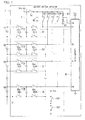
- FIG 1 schematically illustrates a battery voltage controller 1 according to an embodiment of the present invention.
- the battery voltage controller 1 includes: cell voltage detection circuits D1 to DN provided respectively for the battery cells B1 to BN; a charge transfer circuit E; and a microcomputer (voltage controller) M.
- the n-th cell voltage detection circuit (n is an integer of 1 to N), which is appended with a reference symbol Dn, includes: a flying capacitor (voltage detection capacitor) FCn; a first input switch Sna; a second input switch Snb; a first output switch Snc; and a second output switch Snd.
- the flying capacitor FCn is a capacitor that temporarily stores electric charge of a voltage between terminals (cell voltage) of the n-th battery cell Bn.
- the first input switch Sna, the second input switch Snb, and the first output switch Snc, and the second output switch Snd are switching elements such as MOSFET (Metal Oxide Semiconductor-Field Effect Transistor), the on/off-state of which are controlled by the microcomputer M.
- MOSFET Metal Oxide Semiconductor-Field Effect Transistor
- the charge transfer circuit E includes: a charge transfer capacitor MC; N first charge transfer switches SX1 to SXN; two second charge switches SY1 and SY2; a regeneration switch SZ; and two voltage dividing resistors R1 and R2.
- the charge transfer capacitor MC is a capacitor to be used for transferring electric charge between flying capacitors.
- the first charge transfer switches SX1 to SXN, the second charge transfer switches SY1 and SY2, and the regeneration switch SZ are switching elements such as MOSFET, the on/off-state of which are controlled by the microcomputer M.
- One terminal of the flying capacitor FCn is connected to a positive electrode terminal of the battery cell Bn via the first input switch Sna, and is connected to the n-th cell voltage input port Pn of the microcomputer M via the first output switch Snc. Additionally, the one terminal of the flying capacitor FCn is connected to one terminal of the charge transfer capacitor MC via the first output switch Snc and the n-th first charge transfer switch SXn.
- the other terminal of the flying capacitor FCn is connected to a negative electrode terminal of the battery cell Bn via the second input switch Snb, and is connected to a power voltage line (for example, a 5V-Vcc line) in the battery voltage controller 1 via the second output switch Snd and the second charge transfer switch SY1.
- the other terminal of the flying capacitor FCn is connected to a common potential line (for example, a ground line) in the battery voltage controller 1 via the second output switch Snd and the second charge transfer switch SY2.
- the one terminal of the charge transfer capacitor MC is connected to the first charge transfer switches SX1 to SXN Additionally, the one terminal of the charge transfer capacitor MC is connected to the Vcc line via the regeneration switch SZ, and is connected to one terminal of the voltage dividing resistor R1. The other terminal of the charge transfer capacitor MC is connected to the ground line.
- the voltage dividing resistors R1 and R2 are connected in series. One terminal of the voltage dividing resistor R2 is connected to the ground line. Additionally, a terminal of the voltage dividing resistor R2, which is on the high potential side thereof (i.e., the terminal connected to the voltage dividing resistor R1) is connected to a monitor voltage input port Pm of the microcomputer M.
- connection state between the n-th cell voltage detection circuit Dn and the charge transfer circuit E has been explained above, the connection state is common to all the cell voltage detection circuits D1 to DN.
- the connection state is common to all the cell voltage detection circuits D1 to DN.
- one terminal of the flying capacitor FC1 is connected to the positive electrode terminal of the battery cell B1 via the first input switch Sla, and is connected to the cell voltage input port P1 of the microcomputer M via the first output switch S1c.
- the one terminal of the flying capacitor FC1 is connected to one terminal of the charge transfer capacitor MC via the first output switch S1c and the first charge transfer switch SX1.
- the other terminal of the flying capacitor FC1 is connected to the negative electrode terminal of the battery cell B1 via the second input switch S1b, and is connected to the Vcc line via the second output switch Sld and the second charge transfer switch SY1. Additionally, the other terminal of the flying capacitor FC1 is connected to the ground line via the second output switch S1d and the second charge transfer switch SY2.
- the same connection state applies to the other cell voltage detection circuits D2 to DN (may substitute a different number in n), and therefore explanations thereof are omitted here.
- the cell voltage detection circuit Dn having the aforementioned configuration outputs a voltage V_FCn between the terminals of the flying capacitor FCn to the cell voltage input port Pn of the microcomputer M after the battery cell Bn charges the flying capacitor FCn (which is common to all the cell voltage detection circuits D1 to DN).
- the charge transfer circuit E transfers electric charge from a flying capacitor as a charge transferring source to the charge transfer capacitor MC, and thereafter from the charge transfer capacitor MC to a flying capacitor as a charge transferring destination.
- the microcomputer M is a microcomputer including a memory such as a ROM or a RAM, a CPU (Central Processing Unit), an A/D conversion circuit, an input/output interface, and the like.
- the microcomputer M controls on/off-state of each switch to obtain, as the results of the voltage detection for the respective battery cells B1 to BN, output voltages of the respective cell voltage detection circuits D1 to DN (i.e., the voltage between terminals of each of the flying capacitors FC1 to FCN). Based on the results of the voltage detection, the microcomputer M performs voltage balance control of the battery cells B1 to BN.
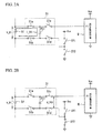
- FIGS. 2A and 2B illustrate on/off-state of each switch at the time of the cell voltage detection by the respective battery cells B1 to BN.
- the state of each switch of the cell voltage detection circuits D1 to DN at the time of the cell voltage detection is the same.
- the microcomputer M first controls the first input switch Sla and the second input switch S1b of the cell voltage detection circuit D1 to be on-state (all the other switches are off-state).
- the flying capacitor FC1 of the cell voltage detection circuit D1 is connected in parallel to the battery cell B1, and thus is charged by a charging current I_B1 as indicated by an arrow shown in FIG 2A .
- the voltage V_FC1 between the terminals of the flying capacitor FC1 becomes equal to the voltage V_B1 between the terminals of the battery cell B1 (cell voltage)
- the flying capacitor FC1 enters a fully-charged state and the charging is completed.
- the microcomputer M controls the first input switch Sla and the second input switch S1b of the cell voltage detection circuit D1 to be off-state. Additionally, the microcomputer M controls the first output switch S1c, the second output switch S1d, and the second charge transfer switch SY2 to be on-state, as shown in FIG 2B . Thereby, one terminal of the flying capacitor FC1 is connected to the cell voltage input port P1 of the microcomputer M. Additionally, the other terminal of the flying capacitor FC1 is connected to the ground line. Consequently, the voltage V_FC1 between the terminals of the flying capacitor FC1 is output to the cell voltage input port P1 of the microcomputer M.
- the microcomputer M obtains the input voltage of the cell voltage input port P 1 (i.e., the voltage V_FC1 between the terminals of the flying capacitor FCI) as the cell voltage V_B1 of the first battery cell B1. Then, the microcomputer M causes the A/D conversion circuit to convert the cell voltage V_B1 into digital data that can be processed by the CPU. Then, the microcomputer M stores, as the result of the cell voltage detection, the digital data in an internal memory (for example, RAM). The microcomputer M performs the aforementioned switch control and the signal process on all the cell voltage detection circuits D1 to DN, thereby obtaining the cell voltage detection results (V_B1 to V_BN) for the respective voltage cells B1 to BN.
- the microcomputer M performs the aforementioned switch control and the signal process on all the cell voltage detection circuits D1 to DN, thereby obtaining the cell voltage detection results (V_B1 to V_BN) for the respective voltage cells B1 to BN.
- the microcomputer M determines whether or not there is a battery cell higher in cell voltage (SOC) than other battery cells. If there is a battery cell higher in cell voltage than other battery cells, the microcomputer M determines, as a charge transferring source, a flying capacitor charged by that battery cell with the high cell voltage.
- SOC cell voltage
- the microcomputer M obtains, as a monitor voltage, an input voltage of the monitor voltage input port Pm (voltage Vm between the terminals of the voltage dividing resistor R2). Then, the microcomputer M causes the A/D conversion circuit to convert the monitor voltage Vm into digital data that can be processed by the CPU. Then, the microcomputer M calculates a voltage V_MC between the terminals of the charge transfer capacitor MC from the monitor voltage Vm by the following formula (1) where r1 denotes a resistance value of the voltage dividing resistor R1, and r2 denotes a resistance value of the voltage dividing resistor R2.
- V_MC r ⁇ 1 + r ⁇ 2 ⁇ Vm / r ⁇ 2
- the microcomputer M compares the voltage V_MC between the terminals of the charge transfer capacitor MC calculated in the above manner to the voltage V_FC 1 between the terminals of the flying capacitor FC1 determined as the charge transferring source (i.e., the cell voltage V_B1). IfV_FCl is higher than V_MC, the microcomputer M controls the charge transfer circuit E to transfer electric charge from the flying capacitor FC1 determined as the charge transferring source to the charge transfer capacitor MC.
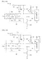
- the microcomputer M controls the first charge transfer switch SX1 and the second charge transfer switch SY1 of the charge transfer circuit E to be on-state, and controls the second charge transfer switch SY2 to be off-state, as shown in FIG 3A .
- one terminal of the flying capacitor FC1 is connected to the charge transfer capacitor MC, and the other terminal of the flying capacitor FC1 is connected to the Vcc line.
- the electric charge stored in the flying capacitor FC1 is transferred to the charge transfer capacitor MC, the charge transfer capacitor MC is charged by a charging current Ic as indicated by an arrow shown in FIG 3A .
- the microcomputer M determines, as a charge transferring destination, a flying capacitor charged by that battery cell with the low cell voltage.
- SOC cell voltage
- the microcomputer M compares the voltage V_MC between the terminals of the charge transferring capacitor MC calculated in the above manner to the voltage V_FC3 between the terminals of the flying capacitor FC3 determined as the charge transferring destination (i.e., the cell voltage V_B3). If V_FC3 is lower than V_MC, the microcomputer M controls the charge transfer circuit E to transfer electric charge from the charge transfer capacitor MC to the flying capacitor FC3 determined as the charge transferring destination.
- V_FC3 if V_FC3 is lower than V_MC, the microcomputer M controls the first charge transfer switch SX3 and the second charge transfer switch SY2 of the charge transfer circuit E to be on-state, and controls the second charge transfer switch SY1 to be off-state, as shown in FIG 3B .
- one terminal of the flying capacitor FC3 is connected to the charge transfer capacitor MC, and the other terminal of the flying capacitor FC3 is connected to the ground line.
- the electric charge stored in the charge transfer capacitor MC is transferred to the flying capacitor FC3, and thereby the flying capacitor FC3 is charged by a charging current Irc as indicated by an arrow shown in FIG 3B .
- the voltage V_FC3 between the terminals of the charged flying capacitor FC3 is higher than the cell voltage V_B3 of the battery cell B3. For this reason, if the next cell voltage detection operation is performed in which the first input switch S3a and the second input switch S3b of the cell voltage detection circuit D3 are controlled to be on-state (other switches are off-state), the battery cell B3 is charged by a charging current I_FC3 as indicated by an arrow shown in FIG 4A , thereby increasing the cell voltage V_B3 of the battery cell B3 (i.e., equalizing cell voltages).
- part of the electric energy of a battery cell which has been wastefully consumed in the related art that is, the electric charge stored in a battery cell
- SOC high cell voltage
- SOC low cell voltage
- the microcomputer M determines, based on the cell voltage detection results (V_B1 to V_BN) of the respective battery cells B1 to BN stored in the internal memory, that the all the battery cells B to BN are in the fully-charged state (i.e., if there is no need to perform voltage balance control), the microcomputer M controls the regeneration circuit switch SZ to be on-state. Thereby, one terminal of the charge transfer capacitor MC is connected to the Vcc line, and a regeneration current Irg flows in the microcomputer M as indicated by an arrow shown in FIG 4B . In other words, if there is no need to perform voltage balance control, the electric charge stored in the charge transfer capacitor MC, that is, electric energy, is supplied to the Vcc line, thereby reducing power consumption of the battery voltage controller 1.
- the present invention is not limited to the above embodiments, and may be modified and changed without departing from the scope and spirit of the invention.
- the charge transfer circuit E having the circuit configuration as shown in FIG 1 has been taken as an example in the above embodiment.
- any circuit configuration may be used as long as electric charge can be transferred from a flying capacitor as a charge transferring source to a flying capacitor as a charge transferring destination.
Landscapes
- Engineering & Computer Science (AREA)
- Power Engineering (AREA)
- Life Sciences & Earth Sciences (AREA)
- Sustainable Development (AREA)
- Sustainable Energy (AREA)
- Transportation (AREA)
- Mechanical Engineering (AREA)
- Charge And Discharge Circuits For Batteries Or The Like (AREA)
- Secondary Cells (AREA)
Abstract
Description
- The present invention relates to a battery voltage controller.
- Priority is claimed on Japanese Patent Application No.
2011-074933, filed March 30, 2011 - As known, a vehicle, such as an electric car or a hybrid car, is provided with a motor, and a high-voltage and high-capacity battery that supplies power to the motor. The battery includes multiple battery cells connected in series. The battery cell includes a lithium-ion battery, a nickel-metal hydride battery, or the like. In related art, a voltage balance control of monitoring and equalizing cell voltages of the battery cells is performed to maintain the performance of the battery.
- For example, Japanese Patent Laid-Open Publication No.
2008-21589 2010-88179 - In the related art, however, part of electric charge stored in the battery cell in the overcharged state is discharged by the discharge circuits in order to equalize the cell voltages. In other words, part of electric energy stored in the battery cell is wastefully consumed as thermal energy. In view of energy efficiency, there has been demand for improvement.
- The present invention has been made in view of the above situations. An object of the present invention is to provide a battery voltage controller that can enhance the energy efficiency at the time of voltage balance control.
- To solve the above problem, a battery voltage controller according to one aspect of the present invention includes, but is not limited to: a plurality of voltage detection circuits; a voltage controller; and a charge transfer circuit. The voltage detection circuits respectively include a plurality of voltage detection capacitors. Each of the voltage detection circuits is configured to output a voltage between terminals of one of the voltage detection capacitors after the voltage detection capacitors are respectively charged by a plurality of battery cells. The voltage controller is configured to obtain output voltages of the voltage detection circuits as results of voltage detection for the battery cells, and perform voltage balance control of the battery cells based on the results of the voltage detection. The charge transfer circuit is configured to transfer electric charge from one of the voltage detection capacitors to a charge transfer capacitor according to control by the voltage controller, and transfer electric charge from the charge transfer capacitor to another one of the voltage detection capacitors.
- If a first battery cell of the battery cells is higher in cell voltage than other battery cells of the battery cells as the results of the voltage detection, the voltage controller may be configured to determine, as a charge transferring source, a first voltage detection capacitor of the voltage detection capacitors which is charged by the first battery cell, and control the charge transfer circuit to transfer electric charge from the first voltage detection capacitor to the charge transfer capacitor.
- The voltage controller may be configured to monitor a voltage between terminals of the charge transfer capacitor. If a voltage between terminals of the first voltage detection capacitor is higher than the voltage between the terminals of the charge transfer capacitor, the voltage controller may be configured to control the charge transfer circuit to transfer the electric charge from the first voltage detection capacitor to the charge transfer capacitor.
- If a second battery cell of the battery cells is lower in cell voltage than other battery cells of the battery cells as the results of the voltage detection, the voltage controller may be configured to determine, as a charge transferring destination, a second voltage detection capacitor of the voltage detection capacitors which is charged by the second battery cell, and control the charge transfer circuit to transfer electric charge from the charge transfer capacitor to the second voltage detection capacitor.
- The voltage controller may be configured to monitor a voltage between terminals of the charge transfer capacitor. If a voltage between terminals of the second voltage detection capacitor is lower than the voltage between the terminals of the charge transfer capacitor, the voltage controller may be configured to control the charge transfer circuit to transfer the electric charge from the charge transfer capacitor to the second voltage detection capacitor.
- One of the terminals of the charge transfer capacitor which is on a high potential side may be connected to a power voltage line via a regeneration switch. The voltage controller may be configured to control the regeneration switch to be on-state if the voltage controller determines, based on the results of the voltage detection, that all of the battery cells are fully charged.
- According to the present invention, part of electric energy stored in the battery cell, which has been wastefully consumed as thermal energy, that is, electric charge stored in the battery cell, can be transferred from a battery cell with a high cell voltage (high SOC) to a battery cell with a low cell voltage (low SOC), thereby equalizing cell voltages. Accordingly, it is possible to enhance the energy efficiency at the time of voltage balance control.
- The above features and advantages of the present invention will be more apparent from the following description of certain preferred embodiments taken in conjunction with the accompanying drawings, in which:
-
FIG 1 schematically illustrates a configuration of abattery voltage controller 1 according to an embodiment of the present invention; and -
FIGS. 2A to 4B illustrate operation of thebattery voltage controller 1. - The present invention will now be described herein with reference to illustrative embodiments. The accompanying drawings explain a battery voltage controller. The size, the thickness, and the like of each illustrated portion might be different from those of each portion of an actual battery voltage controller.
- Those skilled in the art will recognize that many alternative embodiments can be accomplished using the teachings of the present invention and that the present invention is not limited to the embodiments illustrated herein for explanatory purposes.
-
FIG 1 schematically illustrates abattery voltage controller 1 according to an embodiment of the present invention. As shown inFIG 1 , thebattery voltage controller 1 is an ECU (Electronic Control Unit) that detects cell voltages of N battery cells B1 to BN connected in series (for example, N=12), and performs voltage balance control of the battery cells B1 to BN based on results of the cell voltage detection. Thebattery voltage controller 1 includes: cell voltage detection circuits D1 to DN provided respectively for the battery cells B1 to BN; a charge transfer circuit E; and a microcomputer (voltage controller) M. - Each of the cell voltage detection circuits D1 to DN has the same circuit configuration. In other words, the n-th cell voltage detection circuit (n is an integer of 1 to N), which is appended with a reference symbol Dn, includes: a flying capacitor (voltage detection capacitor) FCn; a first input switch Sna; a second input switch Snb; a first output switch Snc; and a second output switch Snd.
- The flying capacitor FCn is a capacitor that temporarily stores electric charge of a voltage between terminals (cell voltage) of the n-th battery cell Bn. The first input switch Sna, the second input switch Snb, and the first output switch Snc, and the second output switch Snd are switching elements such as MOSFET (Metal Oxide Semiconductor-Field Effect Transistor), the on/off-state of which are controlled by the microcomputer M.
- The charge transfer circuit E includes: a charge transfer capacitor MC; N first charge transfer switches SX1 to SXN; two second charge switches SY1 and SY2; a regeneration switch SZ; and two voltage dividing resistors R1 and R2. The charge transfer capacitor MC is a capacitor to be used for transferring electric charge between flying capacitors. The first charge transfer switches SX1 to SXN, the second charge transfer switches SY1 and SY2, and the regeneration switch SZ are switching elements such as MOSFET, the on/off-state of which are controlled by the microcomputer M.
- One terminal of the flying capacitor FCn is connected to a positive electrode terminal of the battery cell Bn via the first input switch Sna, and is connected to the n-th cell voltage input port Pn of the microcomputer M via the first output switch Snc. Additionally, the one terminal of the flying capacitor FCn is connected to one terminal of the charge transfer capacitor MC via the first output switch Snc and the n-th first charge transfer switch SXn.
- The other terminal of the flying capacitor FCn is connected to a negative electrode terminal of the battery cell Bn via the second input switch Snb, and is connected to a power voltage line (for example, a 5V-Vcc line) in the
battery voltage controller 1 via the second output switch Snd and the second charge transfer switch SY1. The other terminal of the flying capacitor FCn is connected to a common potential line (for example, a ground line) in thebattery voltage controller 1 via the second output switch Snd and the second charge transfer switch SY2. - The one terminal of the charge transfer capacitor MC is connected to the first charge transfer switches SX1 to SXN Additionally, the one terminal of the charge transfer capacitor MC is connected to the Vcc line via the regeneration switch SZ, and is connected to one terminal of the voltage dividing resistor R1. The other terminal of the charge transfer capacitor MC is connected to the ground line. The voltage dividing resistors R1 and R2 are connected in series. One terminal of the voltage dividing resistor R2 is connected to the ground line. Additionally, a terminal of the voltage dividing resistor R2, which is on the high potential side thereof (i.e., the terminal connected to the voltage dividing resistor R1) is connected to a monitor voltage input port Pm of the microcomputer M.
- Although the connection state between the n-th cell voltage detection circuit Dn and the charge transfer circuit E has been explained above, the connection state is common to all the cell voltage detection circuits D1 to DN. For example, regarding the first cell voltage detection circuit D1 (n=1), one terminal of the flying capacitor FC1 is connected to the positive electrode terminal of the battery cell B1 via the first input switch Sla, and is connected to the cell voltage input port P1 of the microcomputer M via the first output switch S1c. Additionally, the one terminal of the flying capacitor FC1 is connected to one terminal of the charge transfer capacitor MC via the first output switch S1c and the first charge transfer switch SX1.
- The other terminal of the flying capacitor FC1 is connected to the negative electrode terminal of the battery cell B1 via the second input switch S1b, and is connected to the Vcc line via the second output switch Sld and the second charge transfer switch SY1. Additionally, the other terminal of the flying capacitor FC1 is connected to the ground line via the second output switch S1d and the second charge transfer switch SY2. The same connection state applies to the other cell voltage detection circuits D2 to DN (may substitute a different number in n), and therefore explanations thereof are omitted here.
- As will be explained in detail later, under switch control of the microcomputer M, the cell voltage detection circuit Dn having the aforementioned configuration outputs a voltage V_FCn between the terminals of the flying capacitor FCn to the cell voltage input port Pn of the microcomputer M after the battery cell Bn charges the flying capacitor FCn (which is common to all the cell voltage detection circuits D1 to DN). Additionally, under the switch control of the microcomputer M, the charge transfer circuit E transfers electric charge from a flying capacitor as a charge transferring source to the charge transfer capacitor MC, and thereafter from the charge transfer capacitor MC to a flying capacitor as a charge transferring destination.
- The microcomputer M is a microcomputer including a memory such as a ROM or a RAM, a CPU (Central Processing Unit), an A/D conversion circuit, an input/output interface, and the like. The microcomputer M controls on/off-state of each switch to obtain, as the results of the voltage detection for the respective battery cells B1 to BN, output voltages of the respective cell voltage detection circuits D1 to DN (i.e., the voltage between terminals of each of the flying capacitors FC1 to FCN). Based on the results of the voltage detection, the microcomputer M performs voltage balance control of the battery cells B1 to BN.
- Hereinafter, operation of the
battery voltage controller 1 having the aforementioned configuration is explained. - First, cell voltage detection operation of the
battery voltage controller 1 is explained hereinafter.FIGS. 2A and 2B illustrate on/off-state of each switch at the time of the cell voltage detection by the respective battery cells B1 to BN. For simplification of explanations, only the first battery cell B1, the cell voltagedetection circuit D 1, the second charge transfer switches SY1 and SY2, and the microcomputer M are shown inFIGS. 2A and 2B , the state of each switch of the cell voltage detection circuits D1 to DN at the time of the cell voltage detection is the same. - As shown in
FIG 2A , the microcomputer M first controls the first input switch Sla and the second input switch S1b of the cell voltage detection circuit D1 to be on-state (all the other switches are off-state). Thereby, the flying capacitor FC1 of the cell voltage detection circuit D1 is connected in parallel to the battery cell B1, and thus is charged by a charging current I_B1 as indicated by an arrow shown inFIG 2A . When the voltage V_FC1 between the terminals of the flying capacitor FC1 becomes equal to the voltage V_B1 between the terminals of the battery cell B1 (cell voltage), the flying capacitor FC1 enters a fully-charged state and the charging is completed. - When the charging of the flying capacitor FC1 by the battery cell B1 is completed, the microcomputer M controls the first input switch Sla and the second input switch S1b of the cell voltage detection circuit D1 to be off-state. Additionally, the microcomputer M controls the first output switch S1c, the second output switch S1d, and the second charge transfer switch SY2 to be on-state, as shown in
FIG 2B . Thereby, one terminal of the flying capacitor FC1 is connected to the cell voltage input port P1 of the microcomputer M. Additionally, the other terminal of the flying capacitor FC1 is connected to the ground line. Consequently, the voltage V_FC1 between the terminals of the flying capacitor FC1 is output to the cell voltage input port P1 of the microcomputer M. - The microcomputer M obtains the input voltage of the cell voltage input port P 1 (i.e., the voltage V_FC1 between the terminals of the flying capacitor FCI) as the cell voltage V_B1 of the first battery cell B1. Then, the microcomputer M causes the A/D conversion circuit to convert the cell voltage V_B1 into digital data that can be processed by the CPU. Then, the microcomputer M stores, as the result of the cell voltage detection, the digital data in an internal memory (for example, RAM). The microcomputer M performs the aforementioned switch control and the signal process on all the cell voltage detection circuits D1 to DN, thereby obtaining the cell voltage detection results (V_B1 to V_BN) for the respective voltage cells B1 to BN.
- Hereinafter, voltage balance control operation of the
battery voltage controller 1 is explained. Based on the cell voltage detection results (V_B1 to V_BN) for the respective voltage cells B1 to BN which are stored in the internal memory, the microcomputer M determines whether or not there is a battery cell higher in cell voltage (SOC) than other battery cells. If there is a battery cell higher in cell voltage than other battery cells, the microcomputer M determines, as a charge transferring source, a flying capacitor charged by that battery cell with the high cell voltage. Hereinafter, explanations are given under the assumption that the flying capacitor FC1 is determined as the charge transferring source. - Then, the microcomputer M obtains, as a monitor voltage, an input voltage of the monitor voltage input port Pm (voltage Vm between the terminals of the voltage dividing resistor R2). Then, the microcomputer M causes the A/D conversion circuit to convert the monitor voltage Vm into digital data that can be processed by the CPU. Then, the microcomputer M calculates a voltage V_MC between the terminals of the charge transfer capacitor MC from the monitor voltage Vm by the following formula (1) where r1 denotes a resistance value of the voltage dividing resistor R1, and r2 denotes a resistance value of the voltage dividing resistor R2.

- The microcomputer M compares the voltage V_MC between the terminals of the charge transfer capacitor MC calculated in the above manner to the
voltage V_FC 1 between the terminals of the flying capacitor FC1 determined as the charge transferring source (i.e., the cell voltage V_B1). IfV_FCl is higher than V_MC, the microcomputer M controls the charge transfer circuit E to transfer electric charge from the flying capacitor FC1 determined as the charge transferring source to the charge transfer capacitor MC. - Specifically, ifV_FCl is higher than V_MC, the microcomputer M controls the first charge transfer switch SX1 and the second charge transfer switch SY1 of the charge transfer circuit E to be on-state, and controls the second charge transfer switch SY2 to be off-state, as shown in
FIG 3A . Thereby, one terminal of the flying capacitor FC1 is connected to the charge transfer capacitor MC, and the other terminal of the flying capacitor FC1 is connected to the Vcc line. At this time, the electric charge stored in the flying capacitor FC1 is transferred to the charge transfer capacitor MC, the charge transfer capacitor MC is charged by a charging current Ic as indicated by an arrow shown inFIG 3A . - On the other hand, if there is a battery cell lower in cell voltage (SOC) than other battery cells, the microcomputer M determines, as a charge transferring destination, a flying capacitor charged by that battery cell with the low cell voltage. Hereinafter, explanations are given under the assumption that the flying capacitor FC3 is determined as the charge transferring destination.
- The microcomputer M compares the voltage V_MC between the terminals of the charge transferring capacitor MC calculated in the above manner to the voltage V_FC3 between the terminals of the flying capacitor FC3 determined as the charge transferring destination (i.e., the cell voltage V_B3). If V_FC3 is lower than V_MC, the microcomputer M controls the charge transfer circuit E to transfer electric charge from the charge transfer capacitor MC to the flying capacitor FC3 determined as the charge transferring destination.
- Specifically, if V_FC3 is lower than V_MC, the microcomputer M controls the first charge transfer switch SX3 and the second charge transfer switch SY2 of the charge transfer circuit E to be on-state, and controls the second charge transfer switch SY1 to be off-state, as shown in
FIG 3B . Thereby, one terminal of the flying capacitor FC3 is connected to the charge transfer capacitor MC, and the other terminal of the flying capacitor FC3 is connected to the ground line. At this time, the electric charge stored in the charge transfer capacitor MC is transferred to the flying capacitor FC3, and thereby the flying capacitor FC3 is charged by a charging current Irc as indicated by an arrow shown inFIG 3B . - After the charging, the voltage V_FC3 between the terminals of the charged flying capacitor FC3 is higher than the cell voltage V_B3 of the battery cell B3. For this reason, if the next cell voltage detection operation is performed in which the first input switch S3a and the second input switch S3b of the cell voltage detection circuit D3 are controlled to be on-state (other switches are off-state), the battery cell B3 is charged by a charging current I_FC3 as indicated by an arrow shown in
FIG 4A , thereby increasing the cell voltage V_B3 of the battery cell B3 (i.e., equalizing cell voltages). - As explained above, according to the present embodiment, part of the electric energy of a battery cell which has been wastefully consumed in the related art, that is, the electric charge stored in a battery cell, can be transferred from a battery cell with a high cell voltage (SOC) to a battery cell with a low cell voltage (SOC) using the flying capacitors FC1 to FCN and the charge transfer capacitor MC, thereby equalizing the cell voltages. Therefore, it is possible to enhance the energy efficiency at the time of voltage balance control.
- Additionally, if the microcomputer M determines, based on the cell voltage detection results (V_B1 to V_BN) of the respective battery cells B1 to BN stored in the internal memory, that the all the battery cells B to BN are in the fully-charged state (i.e., if there is no need to perform voltage balance control), the microcomputer M controls the regeneration circuit switch SZ to be on-state. Thereby, one terminal of the charge transfer capacitor MC is connected to the Vcc line, and a regeneration current Irg flows in the microcomputer M as indicated by an arrow shown in
FIG 4B . In other words, if there is no need to perform voltage balance control, the electric charge stored in the charge transfer capacitor MC, that is, electric energy, is supplied to the Vcc line, thereby reducing power consumption of thebattery voltage controller 1. - It is apparent that the present invention is not limited to the above embodiments, and may be modified and changed without departing from the scope and spirit of the invention. For example, the charge transfer circuit E having the circuit configuration as shown in
FIG 1 has been taken as an example in the above embodiment. However, any circuit configuration may be used as long as electric charge can be transferred from a flying capacitor as a charge transferring source to a flying capacitor as a charge transferring destination. - The term "configured" is used to describe a component, section or part of a device includes hardware and/or software that is constructed and/or programmed to carry out the desired function.
Claims (6)
- A battery voltage controller (1) comprising:a plurality of voltage detection circuits (D1 to DN) respectively including a plurality of voltage detection capacitors, each of the voltage detection circuits being configured to output a voltage between terminals of one of the voltage detection capacitors after the voltage detection capacitors are respectively charged by a plurality of battery cells;a voltage controller (M) configured to obtain output voltages of the voltage detection circuits as results of voltage detection for the battery cells, and perform voltage balance control of the battery cells based on the results of the voltage detection; anda charge transfer circuit (E) configured to transfer electric charge from one of the voltage detection capacitors to a charge transfer capacitor according to control by the voltage controller, and transfer electric charge from the charge transfer capacitor to another one of the voltage detection capacitors.
- The battery voltage controller according to claim 1, wherein if a first battery cell of the battery cells is higher in cell voltage than other battery cells of the battery cells as the results of the voltage detection, the voltage controller is configured to determine, as a charge transferring source, a first voltage detection capacitor of the voltage detection capacitors which is charged by the first battery cell, and control the charge transfer circuit to transfer electric charge from the first voltage detection capacitor to the charge transfer capacitor.
- The battery voltage controller according to claim 2, wherein the voltage controller is configured to monitor a voltage between terminals of the charge transfer capacitor, and
if a voltage between terminals of the first voltage detection capacitor is higher than the voltage between the terminals of the charge transfer capacitor, the voltage controller is configured to control the charge transfer circuit to transfer the electric charge from the first voltage detection capacitor to the charge transfer capacitor. - The battery voltage controller according to claim 1, wherein if a second battery cell of the battery cells is lower in cell voltage than other battery cells of the battery cells as the results of the voltage detection, the voltage controller is configured to determine, as a charge transferring destination, a second voltage detection capacitor of the voltage detection capacitors which is charged by the second battery cell, and control the charge transfer circuit to transfer electric charge from the charge transfer capacitor to the second voltage detection capacitor.
- The battery voltage controller according to claim 4, wherein the voltage controller is configured to monitor a voltage between terminals of the charge transfer capacitor, and
if a voltage between terminals of the second voltage detection capacitor is lower than the voltage between the terminals of the charge transfer capacitor, the voltage controller is configured to control the charge transfer circuit to transfer the electric charge from the charge transfer capacitor to the second voltage detection capacitor. - The battery voltage controller according to any one of claims 1 to 5, wherein one of the terminals of the charge transfer capacitor which is on a high potential side is connected to a power voltage line via a regeneration switch, and
the voltage controller is configured to control the regeneration switch to be on-state if the voltage controller determines, based on the results of the voltage detection, that all of the battery cells are fully charged.
Applications Claiming Priority (1)
| Application Number | Priority Date | Filing Date | Title |
|---|---|---|---|
| JP2011074933A JP5645732B2 (en) | 2011-03-30 | 2011-03-30 | Battery voltage control device |
Publications (2)
| Publication Number | Publication Date |
|---|---|
| EP2506390A1 true EP2506390A1 (en) | 2012-10-03 |
| EP2506390B1 EP2506390B1 (en) | 2016-03-16 |
Family
ID=45976700
Family Applications (1)
| Application Number | Title | Priority Date | Filing Date |
|---|---|---|---|
| EP12161346.7A Not-in-force EP2506390B1 (en) | 2011-03-30 | 2012-03-26 | Battery voltage controller |
Country Status (3)
| Country | Link |
|---|---|
| EP (1) | EP2506390B1 (en) |
| JP (1) | JP5645732B2 (en) |
| CN (1) | CN102738856B (en) |
Cited By (10)
| Publication number | Priority date | Publication date | Assignee | Title |
|---|---|---|---|---|
| US20140266003A1 (en) * | 2013-03-15 | 2014-09-18 | Atieva, Inc. | Cell balancing through a switched capacitor level shifter |
| US9041454B2 (en) | 2013-03-15 | 2015-05-26 | Atieva, Inc. | Bias circuit for a switched capacitor level shifter |
| DE102015117744A1 (en) | 2015-10-19 | 2017-04-20 | Dr. Ing. H.C. F. Porsche Aktiengesellschaft | battery system |
| US9853461B2 (en) | 2013-04-09 | 2017-12-26 | Evtd Inc. | Balance correction apparatus and electric storage system |
| US9966584B2 (en) | 2013-03-11 | 2018-05-08 | Atieva, Inc. | Bus bar for battery packs |
| US10063071B2 (en) | 2013-03-15 | 2018-08-28 | Atieva, Inc. | Balance resistor and low pass filter |
| US10084214B2 (en) | 2013-03-15 | 2018-09-25 | Atieva, Inc. | Automatic switchover from cell voltage to interconnect voltage monitoring |
| US10236704B2 (en) | 2016-04-28 | 2019-03-19 | Yazaki Corporation | Charge collection device and power collection method |
| US10374442B2 (en) | 2013-10-17 | 2019-08-06 | Bosch Battery Systems, Llc | Integrated multiple voltage energy storage system and method |
| US10901019B2 (en) | 2013-03-15 | 2021-01-26 | Atieva, Inc. | Method of connecting cell voltage sensors |
Families Citing this family (8)
| Publication number | Priority date | Publication date | Assignee | Title |
|---|---|---|---|---|
| JP6305159B2 (en) * | 2014-03-31 | 2018-04-04 | Tocキャパシタ株式会社 | Storage module voltage equalization circuit |
| JP6541310B2 (en) | 2014-06-25 | 2019-07-10 | NExT−e Solutions株式会社 | Module control device, balance correction system and storage system |
| JP6231969B2 (en) * | 2014-10-22 | 2017-11-15 | 矢崎総業株式会社 | Voltage equalization apparatus and voltage equalization method |
| CN109347173B (en) * | 2018-11-21 | 2022-05-24 | 西南交通大学 | Battery pack balance control circuit and method based on switched capacitor |
| WO2021085646A1 (en) | 2019-11-01 | 2021-05-06 | NExT-e Solutions株式会社 | Energy storage system |
| JP7388446B2 (en) | 2019-11-25 | 2023-11-29 | 株式会社村田製作所 | battery unit |
| CN111551780B (en) * | 2020-05-15 | 2022-05-13 | 苏州佳智彩光电科技有限公司 | Bidirectional load high-precision current and voltage detection and monitoring method and system |
| CN111679216B (en) * | 2020-06-24 | 2022-08-02 | 重庆长安新能源汽车科技有限公司 | Device and method for detecting high-voltage connection reliability of power battery |
Citations (6)
| Publication number | Priority date | Publication date | Assignee | Title |
|---|---|---|---|---|
| US20040246635A1 (en) * | 2001-10-01 | 2004-12-09 | Koichi Morita | Voltage balance circuit, voltage detective circuit, voltage balancing method, and voltage detecting method |
| US20060261677A1 (en) * | 2005-05-17 | 2006-11-23 | Nobuo Shibuya | Apparatus and method for detecting voltage of assembled battery |
| JP2008021589A (en) | 2006-07-14 | 2008-01-31 | Nissan Motor Co Ltd | Capacity adjustment device |
| US20090309545A1 (en) * | 2008-06-17 | 2009-12-17 | Sanyo Electric Co., Ltd. | Voltage Detecting Device Of Assembled Battery And Assembled Battery System Comprising Same |
| JP2010088179A (en) | 2008-09-30 | 2010-04-15 | Panasonic Corp | Battery equalization circuit, and battery power supply device |
| JP2011074933A (en) | 2009-09-29 | 2011-04-14 | Yamatake Corp | Control valve and method of calibrating real opening converting characteristic of the same |
Family Cites Families (8)
| Publication number | Priority date | Publication date | Assignee | Title |
|---|---|---|---|---|
| JP3099181B2 (en) * | 1996-09-10 | 2000-10-16 | 本田技研工業株式会社 | Battery voltage control device |
| US7193390B2 (en) * | 2002-05-17 | 2007-03-20 | Sony Corporation | Apparatus for connecting secondary battery cells in series and method for controlling secondary battery cells connected in series |
| JP2004120871A (en) * | 2002-09-25 | 2004-04-15 | Yazaki Corp | Method and apparatus for adjusting state of charge of assembled battery |
| JP4305419B2 (en) * | 2005-06-21 | 2009-07-29 | 株式会社デンソー | Battery equalization circuit |
| JP2007040842A (en) * | 2005-08-03 | 2007-02-15 | Matsushita Electric Ind Co Ltd | Voltage measuring device and electric tool |
| JP5060857B2 (en) * | 2007-07-19 | 2012-10-31 | 日立ビークルエナジー株式会社 | Cell controller |
| KR100993080B1 (en) * | 2007-08-08 | 2010-11-08 | 주식회사 엘지화학 | Apparatus and method for measuring battery cell voltage using insulated capacitors |
| JP2009081949A (en) * | 2007-09-26 | 2009-04-16 | Toshiba Corp | Battery protection device and battery pack system including the same |
-
2011
- 2011-03-30 JP JP2011074933A patent/JP5645732B2/en active Active
-
2012
- 2012-03-26 EP EP12161346.7A patent/EP2506390B1/en not_active Not-in-force
- 2012-03-28 CN CN201210085263.8A patent/CN102738856B/en not_active Expired - Fee Related
Patent Citations (6)
| Publication number | Priority date | Publication date | Assignee | Title |
|---|---|---|---|---|
| US20040246635A1 (en) * | 2001-10-01 | 2004-12-09 | Koichi Morita | Voltage balance circuit, voltage detective circuit, voltage balancing method, and voltage detecting method |
| US20060261677A1 (en) * | 2005-05-17 | 2006-11-23 | Nobuo Shibuya | Apparatus and method for detecting voltage of assembled battery |
| JP2008021589A (en) | 2006-07-14 | 2008-01-31 | Nissan Motor Co Ltd | Capacity adjustment device |
| US20090309545A1 (en) * | 2008-06-17 | 2009-12-17 | Sanyo Electric Co., Ltd. | Voltage Detecting Device Of Assembled Battery And Assembled Battery System Comprising Same |
| JP2010088179A (en) | 2008-09-30 | 2010-04-15 | Panasonic Corp | Battery equalization circuit, and battery power supply device |
| JP2011074933A (en) | 2009-09-29 | 2011-04-14 | Yamatake Corp | Control valve and method of calibrating real opening converting characteristic of the same |
Cited By (16)
| Publication number | Priority date | Publication date | Assignee | Title |
|---|---|---|---|---|
| US9966584B2 (en) | 2013-03-11 | 2018-05-08 | Atieva, Inc. | Bus bar for battery packs |
| US12381250B2 (en) | 2013-03-11 | 2025-08-05 | Atieva, Inc. | Bus bars for battery packs |
| US10637110B1 (en) | 2013-03-11 | 2020-04-28 | Atieva, Inc. | Bus bar for battery packs |
| US10063071B2 (en) | 2013-03-15 | 2018-08-28 | Atieva, Inc. | Balance resistor and low pass filter |
| US9584126B2 (en) | 2013-03-15 | 2017-02-28 | Atieva, Inc. | Bias circuit for a switched capacitor level shifter |
| CN105051638A (en) * | 2013-03-15 | 2015-11-11 | 阿提瓦公司 | Bias circuit for a switched capacitor level shifter |
| US20140266003A1 (en) * | 2013-03-15 | 2014-09-18 | Atieva, Inc. | Cell balancing through a switched capacitor level shifter |
| US10084214B2 (en) | 2013-03-15 | 2018-09-25 | Atieva, Inc. | Automatic switchover from cell voltage to interconnect voltage monitoring |
| US9041454B2 (en) | 2013-03-15 | 2015-05-26 | Atieva, Inc. | Bias circuit for a switched capacitor level shifter |
| US10901019B2 (en) | 2013-03-15 | 2021-01-26 | Atieva, Inc. | Method of connecting cell voltage sensors |
| WO2014144279A1 (en) * | 2013-03-15 | 2014-09-18 | Atieva, Inc. | Cell balancing through a switched capacitor level shifter |
| US9853461B2 (en) | 2013-04-09 | 2017-12-26 | Evtd Inc. | Balance correction apparatus and electric storage system |
| US10374442B2 (en) | 2013-10-17 | 2019-08-06 | Bosch Battery Systems, Llc | Integrated multiple voltage energy storage system and method |
| DE102015117744A1 (en) | 2015-10-19 | 2017-04-20 | Dr. Ing. H.C. F. Porsche Aktiengesellschaft | battery system |
| US10135266B2 (en) | 2015-10-19 | 2018-11-20 | Dr. Ing. H.C. F. Porsche Aktiengesellschaft | Battery system for motor vehicle with loss-free switching and automatic charge equalization |
| US10236704B2 (en) | 2016-04-28 | 2019-03-19 | Yazaki Corporation | Charge collection device and power collection method |
Also Published As
| Publication number | Publication date |
|---|---|
| EP2506390B1 (en) | 2016-03-16 |
| CN102738856B (en) | 2016-07-06 |
| CN102738856A (en) | 2012-10-17 |
| JP2012210109A (en) | 2012-10-25 |
| JP5645732B2 (en) | 2014-12-24 |
Similar Documents
| Publication | Publication Date | Title |
|---|---|---|
| EP2506390B1 (en) | Battery voltage controller | |
| CN110249475B (en) | Battery module balancing device and battery pack and vehicle comprising same | |
| EP3185388B1 (en) | Battery control method and apparatus, and battery pack | |
| KR101893045B1 (en) | Charge balancing system for batteries | |
| CN109787306B (en) | Control device, control system, power storage device and control method | |
| US9046584B2 (en) | Battery voltage detector having pull-up resistor | |
| CN112119562B (en) | Storage system | |
| EP3396809B1 (en) | Battery balancing device and method | |
| US10320204B2 (en) | Electric storage apparatus and electric-storage controlling method | |
| US8872476B2 (en) | Charging management system and charger with the same | |
| EP3339086A1 (en) | Motor vehicle and charge and discharge control circuit thereof | |
| CN111630398B (en) | Battery management device, and battery pack and vehicle including the same | |
| JP5168176B2 (en) | Battery pack capacity adjustment device | |
| JP5553061B2 (en) | Cell balance device | |
| CN102856948A (en) | Cell balancing device | |
| CN112119563B (en) | Power storage system | |
| CN110999023A (en) | Method and apparatus for balancing the state of charge of individual cells of a battery system | |
| JP5569418B2 (en) | Battery monitoring device | |
| KR102789132B1 (en) | Controlling Apparatus for turn-on operation of Switch means included in Parallel Multi Battery Pack and Method thereof | |
| KR20150013302A (en) | Charge balancing in a battery | |
| EP3790150B1 (en) | Apparatus and method for battery module balancing | |
| US20150035490A1 (en) | Battery management system and method | |
| WO2016063760A1 (en) | Power supply device, protective device, and protection method | |
| TW202329576A (en) | Method for operating a battery system, battery system | |
| EP2506388A2 (en) | Auxiliary battery charging apparatus |
Legal Events
| Date | Code | Title | Description |
|---|---|---|---|
| PUAI | Public reference made under article 153(3) epc to a published international application that has entered the european phase |
Free format text: ORIGINAL CODE: 0009012 |
|
| AK | Designated contracting states |
Kind code of ref document: A1 Designated state(s): AL AT BE BG CH CY CZ DE DK EE ES FI FR GB GR HR HU IE IS IT LI LT LU LV MC MK MT NL NO PL PT RO RS SE SI SK SM TR |
|
| AX | Request for extension of the european patent |
Extension state: BA ME |
|
| 17P | Request for examination filed |
Effective date: 20130311 |
|
| RIC1 | Information provided on ipc code assigned before grant |
Ipc: H02J 7/00 20060101AFI20140722BHEP Ipc: B60L 11/18 20060101ALI20140722BHEP Ipc: H02J 7/34 20060101ALI20140722BHEP Ipc: G01R 31/36 20060101ALI20140722BHEP |
|
| GRAP | Despatch of communication of intention to grant a patent |
Free format text: ORIGINAL CODE: EPIDOSNIGR1 |
|
| INTG | Intention to grant announced |
Effective date: 20150908 |
|
| GRAS | Grant fee paid |
Free format text: ORIGINAL CODE: EPIDOSNIGR3 |
|
| GRAA | (expected) grant |
Free format text: ORIGINAL CODE: 0009210 |
|
| AK | Designated contracting states |
Kind code of ref document: B1 Designated state(s): AL AT BE BG CH CY CZ DE DK EE ES FI FR GB GR HR HU IE IS IT LI LT LU LV MC MK MT NL NO PL PT RO RS SE SI SK SM TR |
|
| REG | Reference to a national code |
Ref country code: GB Ref legal event code: FG4D |
|
| REG | Reference to a national code |
Ref country code: CH Ref legal event code: EP Ref country code: FR Ref legal event code: PLFP Year of fee payment: 5 |
|
| REG | Reference to a national code |
Ref country code: IE Ref legal event code: FG4D |
|
| REG | Reference to a national code |
Ref country code: AT Ref legal event code: REF Ref document number: 781967 Country of ref document: AT Kind code of ref document: T Effective date: 20160415 |
|
| REG | Reference to a national code |
Ref country code: DE Ref legal event code: R096 Ref document number: 602012015574 Country of ref document: DE |
|
| REG | Reference to a national code |
Ref country code: NL Ref legal event code: MP Effective date: 20160316 |
|
| REG | Reference to a national code |
Ref country code: LT Ref legal event code: MG4D |
|
| PG25 | Lapsed in a contracting state [announced via postgrant information from national office to epo] |
Ref country code: GR Free format text: LAPSE BECAUSE OF FAILURE TO SUBMIT A TRANSLATION OF THE DESCRIPTION OR TO PAY THE FEE WITHIN THE PRESCRIBED TIME-LIMIT Effective date: 20160617 Ref country code: NO Free format text: LAPSE BECAUSE OF FAILURE TO SUBMIT A TRANSLATION OF THE DESCRIPTION OR TO PAY THE FEE WITHIN THE PRESCRIBED TIME-LIMIT Effective date: 20160616 Ref country code: FI Free format text: LAPSE BECAUSE OF FAILURE TO SUBMIT A TRANSLATION OF THE DESCRIPTION OR TO PAY THE FEE WITHIN THE PRESCRIBED TIME-LIMIT Effective date: 20160316 Ref country code: HR Free format text: LAPSE BECAUSE OF FAILURE TO SUBMIT A TRANSLATION OF THE DESCRIPTION OR TO PAY THE FEE WITHIN THE PRESCRIBED TIME-LIMIT Effective date: 20160316 |
|
| REG | Reference to a national code |
Ref country code: AT Ref legal event code: MK05 Ref document number: 781967 Country of ref document: AT Kind code of ref document: T Effective date: 20160316 |
|
| PG25 | Lapsed in a contracting state [announced via postgrant information from national office to epo] |
Ref country code: LT Free format text: LAPSE BECAUSE OF FAILURE TO SUBMIT A TRANSLATION OF THE DESCRIPTION OR TO PAY THE FEE WITHIN THE PRESCRIBED TIME-LIMIT Effective date: 20160316 Ref country code: BE Free format text: LAPSE BECAUSE OF NON-PAYMENT OF DUE FEES Effective date: 20160331 Ref country code: NL Free format text: LAPSE BECAUSE OF FAILURE TO SUBMIT A TRANSLATION OF THE DESCRIPTION OR TO PAY THE FEE WITHIN THE PRESCRIBED TIME-LIMIT Effective date: 20160316 Ref country code: LV Free format text: LAPSE BECAUSE OF FAILURE TO SUBMIT A TRANSLATION OF THE DESCRIPTION OR TO PAY THE FEE WITHIN THE PRESCRIBED TIME-LIMIT Effective date: 20160316 Ref country code: SE Free format text: LAPSE BECAUSE OF FAILURE TO SUBMIT A TRANSLATION OF THE DESCRIPTION OR TO PAY THE FEE WITHIN THE PRESCRIBED TIME-LIMIT Effective date: 20160316 Ref country code: RS Free format text: LAPSE BECAUSE OF FAILURE TO SUBMIT A TRANSLATION OF THE DESCRIPTION OR TO PAY THE FEE WITHIN THE PRESCRIBED TIME-LIMIT Effective date: 20160316 |
|
| PG25 | Lapsed in a contracting state [announced via postgrant information from national office to epo] |
Ref country code: EE Free format text: LAPSE BECAUSE OF FAILURE TO SUBMIT A TRANSLATION OF THE DESCRIPTION OR TO PAY THE FEE WITHIN THE PRESCRIBED TIME-LIMIT Effective date: 20160316 Ref country code: IS Free format text: LAPSE BECAUSE OF FAILURE TO SUBMIT A TRANSLATION OF THE DESCRIPTION OR TO PAY THE FEE WITHIN THE PRESCRIBED TIME-LIMIT Effective date: 20160716 Ref country code: PL Free format text: LAPSE BECAUSE OF FAILURE TO SUBMIT A TRANSLATION OF THE DESCRIPTION OR TO PAY THE FEE WITHIN THE PRESCRIBED TIME-LIMIT Effective date: 20160316 |
|
| REG | Reference to a national code |
Ref country code: CH Ref legal event code: PL |
|
| PG25 | Lapsed in a contracting state [announced via postgrant information from national office to epo] |
Ref country code: PT Free format text: LAPSE BECAUSE OF FAILURE TO SUBMIT A TRANSLATION OF THE DESCRIPTION OR TO PAY THE FEE WITHIN THE PRESCRIBED TIME-LIMIT Effective date: 20160718 Ref country code: AT Free format text: LAPSE BECAUSE OF FAILURE TO SUBMIT A TRANSLATION OF THE DESCRIPTION OR TO PAY THE FEE WITHIN THE PRESCRIBED TIME-LIMIT Effective date: 20160316 Ref country code: SM Free format text: LAPSE BECAUSE OF FAILURE TO SUBMIT A TRANSLATION OF THE DESCRIPTION OR TO PAY THE FEE WITHIN THE PRESCRIBED TIME-LIMIT Effective date: 20160316 Ref country code: ES Free format text: LAPSE BECAUSE OF FAILURE TO SUBMIT A TRANSLATION OF THE DESCRIPTION OR TO PAY THE FEE WITHIN THE PRESCRIBED TIME-LIMIT Effective date: 20160316 Ref country code: RO Free format text: LAPSE BECAUSE OF FAILURE TO SUBMIT A TRANSLATION OF THE DESCRIPTION OR TO PAY THE FEE WITHIN THE PRESCRIBED TIME-LIMIT Effective date: 20160316 Ref country code: CZ Free format text: LAPSE BECAUSE OF FAILURE TO SUBMIT A TRANSLATION OF THE DESCRIPTION OR TO PAY THE FEE WITHIN THE PRESCRIBED TIME-LIMIT Effective date: 20160316 Ref country code: SK Free format text: LAPSE BECAUSE OF FAILURE TO SUBMIT A TRANSLATION OF THE DESCRIPTION OR TO PAY THE FEE WITHIN THE PRESCRIBED TIME-LIMIT Effective date: 20160316 |
|
| REG | Reference to a national code |
Ref country code: DE Ref legal event code: R097 Ref document number: 602012015574 Country of ref document: DE |
|
| REG | Reference to a national code |
Ref country code: IE Ref legal event code: MM4A |
|
| PG25 | Lapsed in a contracting state [announced via postgrant information from national office to epo] |
Ref country code: BE Free format text: LAPSE BECAUSE OF FAILURE TO SUBMIT A TRANSLATION OF THE DESCRIPTION OR TO PAY THE FEE WITHIN THE PRESCRIBED TIME-LIMIT Effective date: 20160316 Ref country code: IT Free format text: LAPSE BECAUSE OF FAILURE TO SUBMIT A TRANSLATION OF THE DESCRIPTION OR TO PAY THE FEE WITHIN THE PRESCRIBED TIME-LIMIT Effective date: 20160316 |
|
| PLBE | No opposition filed within time limit |
Free format text: ORIGINAL CODE: 0009261 |
|
| STAA | Information on the status of an ep patent application or granted ep patent |
Free format text: STATUS: NO OPPOSITION FILED WITHIN TIME LIMIT |
|
| PG25 | Lapsed in a contracting state [announced via postgrant information from national office to epo] |
Ref country code: CH Free format text: LAPSE BECAUSE OF NON-PAYMENT OF DUE FEES Effective date: 20160331 Ref country code: LI Free format text: LAPSE BECAUSE OF NON-PAYMENT OF DUE FEES Effective date: 20160331 Ref country code: DK Free format text: LAPSE BECAUSE OF FAILURE TO SUBMIT A TRANSLATION OF THE DESCRIPTION OR TO PAY THE FEE WITHIN THE PRESCRIBED TIME-LIMIT Effective date: 20160316 Ref country code: IE Free format text: LAPSE BECAUSE OF NON-PAYMENT OF DUE FEES Effective date: 20160326 |
|
| REG | Reference to a national code |
Ref country code: FR Ref legal event code: PLFP Year of fee payment: 6 |
|
| 26N | No opposition filed |
Effective date: 20161219 |
|
| PG25 | Lapsed in a contracting state [announced via postgrant information from national office to epo] |
Ref country code: BG Free format text: LAPSE BECAUSE OF FAILURE TO SUBMIT A TRANSLATION OF THE DESCRIPTION OR TO PAY THE FEE WITHIN THE PRESCRIBED TIME-LIMIT Effective date: 20160616 |
|
| GBPC | Gb: european patent ceased through non-payment of renewal fee |
Effective date: 20160616 |
|
| PG25 | Lapsed in a contracting state [announced via postgrant information from national office to epo] |
Ref country code: SI Free format text: LAPSE BECAUSE OF FAILURE TO SUBMIT A TRANSLATION OF THE DESCRIPTION OR TO PAY THE FEE WITHIN THE PRESCRIBED TIME-LIMIT Effective date: 20160316 Ref country code: GB Free format text: LAPSE BECAUSE OF NON-PAYMENT OF DUE FEES Effective date: 20160616 |
|
| PG25 | Lapsed in a contracting state [announced via postgrant information from national office to epo] |
Ref country code: MT Free format text: LAPSE BECAUSE OF FAILURE TO SUBMIT A TRANSLATION OF THE DESCRIPTION OR TO PAY THE FEE WITHIN THE PRESCRIBED TIME-LIMIT Effective date: 20160316 |
|
| REG | Reference to a national code |
Ref country code: FR Ref legal event code: PLFP Year of fee payment: 7 |
|
| PG25 | Lapsed in a contracting state [announced via postgrant information from national office to epo] |
Ref country code: HU Free format text: LAPSE BECAUSE OF FAILURE TO SUBMIT A TRANSLATION OF THE DESCRIPTION OR TO PAY THE FEE WITHIN THE PRESCRIBED TIME-LIMIT; INVALID AB INITIO Effective date: 20120326 Ref country code: CY Free format text: LAPSE BECAUSE OF FAILURE TO SUBMIT A TRANSLATION OF THE DESCRIPTION OR TO PAY THE FEE WITHIN THE PRESCRIBED TIME-LIMIT Effective date: 20160316 |
|
| PG25 | Lapsed in a contracting state [announced via postgrant information from national office to epo] |
Ref country code: LU Free format text: LAPSE BECAUSE OF NON-PAYMENT OF DUE FEES Effective date: 20160326 Ref country code: MC Free format text: LAPSE BECAUSE OF FAILURE TO SUBMIT A TRANSLATION OF THE DESCRIPTION OR TO PAY THE FEE WITHIN THE PRESCRIBED TIME-LIMIT Effective date: 20160316 Ref country code: TR Free format text: LAPSE BECAUSE OF FAILURE TO SUBMIT A TRANSLATION OF THE DESCRIPTION OR TO PAY THE FEE WITHIN THE PRESCRIBED TIME-LIMIT Effective date: 20160316 Ref country code: MK Free format text: LAPSE BECAUSE OF FAILURE TO SUBMIT A TRANSLATION OF THE DESCRIPTION OR TO PAY THE FEE WITHIN THE PRESCRIBED TIME-LIMIT Effective date: 20160316 Ref country code: MT Free format text: LAPSE BECAUSE OF FAILURE TO SUBMIT A TRANSLATION OF THE DESCRIPTION OR TO PAY THE FEE WITHIN THE PRESCRIBED TIME-LIMIT Effective date: 20160331 |
|
| PG25 | Lapsed in a contracting state [announced via postgrant information from national office to epo] |
Ref country code: AL Free format text: LAPSE BECAUSE OF FAILURE TO SUBMIT A TRANSLATION OF THE DESCRIPTION OR TO PAY THE FEE WITHIN THE PRESCRIBED TIME-LIMIT Effective date: 20160316 |
|
| REG | Reference to a national code |
Ref country code: DE Ref legal event code: R081 Ref document number: 602012015574 Country of ref document: DE Owner name: HITACHI ASTEMO, LTD., HITACHINAKA-SHI, JP Free format text: FORMER OWNER: KEIHIN CORPORATION, TOKYO, JP |
|
| PGFP | Annual fee paid to national office [announced via postgrant information from national office to epo] |
Ref country code: DE Payment date: 20220203 Year of fee payment: 11 |
|
| PGFP | Annual fee paid to national office [announced via postgrant information from national office to epo] |
Ref country code: FR Payment date: 20220209 Year of fee payment: 11 |
|
| REG | Reference to a national code |
Ref country code: DE Ref legal event code: R119 Ref document number: 602012015574 Country of ref document: DE |
|
| PG25 | Lapsed in a contracting state [announced via postgrant information from national office to epo] |
Ref country code: FR Free format text: LAPSE BECAUSE OF NON-PAYMENT OF DUE FEES Effective date: 20230331 Ref country code: DE Free format text: LAPSE BECAUSE OF NON-PAYMENT OF DUE FEES Effective date: 20231003 |