EP2503536A1 - Aktive Matrix-Elektrolumineszenzanzeige - Google Patents
Aktive Matrix-Elektrolumineszenzanzeige Download PDFInfo
- Publication number
- EP2503536A1 EP2503536A1 EP11006463A EP11006463A EP2503536A1 EP 2503536 A1 EP2503536 A1 EP 2503536A1 EP 11006463 A EP11006463 A EP 11006463A EP 11006463 A EP11006463 A EP 11006463A EP 2503536 A1 EP2503536 A1 EP 2503536A1
- Authority
- EP
- European Patent Office
- Prior art keywords
- pixel circuits
- emission
- display device
- buffer
- row
- Prior art date
- Legal status (The legal status is an assumption and is not a legal conclusion. Google has not performed a legal analysis and makes no representation as to the accuracy of the status listed.)
- Withdrawn
Links
- 239000011159 matrix material Substances 0.000 title claims abstract description 22
- 230000002093 peripheral effect Effects 0.000 claims description 10
- 238000000034 method Methods 0.000 claims description 7
- 239000004065 semiconductor Substances 0.000 claims description 6
- 239000010409 thin film Substances 0.000 claims description 4
- 229910044991 metal oxide Inorganic materials 0.000 claims description 3
- 150000004706 metal oxides Chemical class 0.000 claims description 3
- 230000000295 complement effect Effects 0.000 claims description 2
- 229920001621 AMOLED Polymers 0.000 description 29
- 238000010586 diagram Methods 0.000 description 7
- 239000003990 capacitor Substances 0.000 description 3
- 238000012986 modification Methods 0.000 description 3
- 230000004048 modification Effects 0.000 description 3
- 239000007787 solid Substances 0.000 description 3
- 239000000758 substrate Substances 0.000 description 3
- 239000011521 glass Substances 0.000 description 2
- 239000000463 material Substances 0.000 description 2
- 230000000903 blocking effect Effects 0.000 description 1
- 238000010276 construction Methods 0.000 description 1
- 230000007812 deficiency Effects 0.000 description 1
- 238000000151 deposition Methods 0.000 description 1
- 239000010408 film Substances 0.000 description 1
- 239000012212 insulator Substances 0.000 description 1
- 239000004973 liquid crystal related substance Substances 0.000 description 1
- 150000002894 organic compounds Chemical class 0.000 description 1
- 238000007493 shaping process Methods 0.000 description 1
Images


Classifications
-
- G—PHYSICS
- G09—EDUCATION; CRYPTOGRAPHY; DISPLAY; ADVERTISING; SEALS
- G09G—ARRANGEMENTS OR CIRCUITS FOR CONTROL OF INDICATING DEVICES USING STATIC MEANS TO PRESENT VARIABLE INFORMATION
- G09G3/00—Control arrangements or circuits, of interest only in connection with visual indicators other than cathode-ray tubes
- G09G3/20—Control arrangements or circuits, of interest only in connection with visual indicators other than cathode-ray tubes for presentation of an assembly of a number of characters, e.g. a page, by composing the assembly by combination of individual elements arranged in a matrix no fixed position being assigned to or needed to be assigned to the individual characters or partial characters
- G09G3/22—Control arrangements or circuits, of interest only in connection with visual indicators other than cathode-ray tubes for presentation of an assembly of a number of characters, e.g. a page, by composing the assembly by combination of individual elements arranged in a matrix no fixed position being assigned to or needed to be assigned to the individual characters or partial characters using controlled light sources
- G09G3/30—Control arrangements or circuits, of interest only in connection with visual indicators other than cathode-ray tubes for presentation of an assembly of a number of characters, e.g. a page, by composing the assembly by combination of individual elements arranged in a matrix no fixed position being assigned to or needed to be assigned to the individual characters or partial characters using controlled light sources using electroluminescent panels
- G09G3/32—Control arrangements or circuits, of interest only in connection with visual indicators other than cathode-ray tubes for presentation of an assembly of a number of characters, e.g. a page, by composing the assembly by combination of individual elements arranged in a matrix no fixed position being assigned to or needed to be assigned to the individual characters or partial characters using controlled light sources using electroluminescent panels semiconductive, e.g. using light-emitting diodes [LED]
- G09G3/3208—Control arrangements or circuits, of interest only in connection with visual indicators other than cathode-ray tubes for presentation of an assembly of a number of characters, e.g. a page, by composing the assembly by combination of individual elements arranged in a matrix no fixed position being assigned to or needed to be assigned to the individual characters or partial characters using controlled light sources using electroluminescent panels semiconductive, e.g. using light-emitting diodes [LED] organic, e.g. using organic light-emitting diodes [OLED]
- G09G3/3266—Details of drivers for scan electrodes
-
- H—ELECTRICITY
- H10—SEMICONDUCTOR DEVICES; ELECTRIC SOLID-STATE DEVICES NOT OTHERWISE PROVIDED FOR
- H10K—ORGANIC ELECTRIC SOLID-STATE DEVICES
- H10K59/00—Integrated devices, or assemblies of multiple devices, comprising at least one organic light-emitting element covered by group H10K50/00
- H10K59/10—OLED displays
- H10K59/12—Active-matrix OLED [AMOLED] displays
- H10K59/121—Active-matrix OLED [AMOLED] displays characterised by the geometry or disposition of pixel elements
-
- G—PHYSICS
- G09—EDUCATION; CRYPTOGRAPHY; DISPLAY; ADVERTISING; SEALS
- G09G—ARRANGEMENTS OR CIRCUITS FOR CONTROL OF INDICATING DEVICES USING STATIC MEANS TO PRESENT VARIABLE INFORMATION
- G09G2300/00—Aspects of the constitution of display devices
- G09G2300/04—Structural and physical details of display devices
- G09G2300/0404—Matrix technologies
- G09G2300/0408—Integration of the drivers onto the display substrate
-
- G—PHYSICS
- G09—EDUCATION; CRYPTOGRAPHY; DISPLAY; ADVERTISING; SEALS
- G09G—ARRANGEMENTS OR CIRCUITS FOR CONTROL OF INDICATING DEVICES USING STATIC MEANS TO PRESENT VARIABLE INFORMATION
- G09G2300/00—Aspects of the constitution of display devices
- G09G2300/04—Structural and physical details of display devices
- G09G2300/0439—Pixel structures
-
- G—PHYSICS
- G09—EDUCATION; CRYPTOGRAPHY; DISPLAY; ADVERTISING; SEALS
- G09G—ARRANGEMENTS OR CIRCUITS FOR CONTROL OF INDICATING DEVICES USING STATIC MEANS TO PRESENT VARIABLE INFORMATION
- G09G2310/00—Command of the display device
- G09G2310/02—Addressing, scanning or driving the display screen or processing steps related thereto
- G09G2310/0264—Details of driving circuits
- G09G2310/0267—Details of drivers for scan electrodes, other than drivers for liquid crystal, plasma or OLED displays
-
- G—PHYSICS
- G09—EDUCATION; CRYPTOGRAPHY; DISPLAY; ADVERTISING; SEALS
- G09G—ARRANGEMENTS OR CIRCUITS FOR CONTROL OF INDICATING DEVICES USING STATIC MEANS TO PRESENT VARIABLE INFORMATION
- G09G2320/00—Control of display operating conditions
- G09G2320/02—Improving the quality of display appearance
- G09G2320/0223—Compensation for problems related to R-C delay and attenuation in electrodes of matrix panels, e.g. in gate electrodes or on-substrate video signal electrodes
Definitions
- the present invention relates generally to an active matrix electroluminescent display, and more particularly, to an active matrix organic light emitting diode (AMOLED) display with a slim border.
- AMOLED active matrix organic light emitting diode
- OLED displays are used as television screens, computer monitors, portable electronic systems such as mobile phones and personal digital assistants (PDAs).
- An OLED is a light emitting diode (LED) in which the emissive electroluminescent layer is a film of organic compounds which emit light in response to an electric current. This layer of organic semiconductor material is situated between two electrodes. Generally, at least one of these electrodes is transparent.
- An OLED display functions without a backlight. Thus, it can display deep black levels and can also he thinner and lighter than other flat panel displays such liquid crystal displays (LCDs).
- OLED displays can use either passive-matrix (PMOLED) or active-matrix (AMOLED) addressing schemes. AMOLED is more suitable for higher resolution and larger size displays.
- An AMOLED display normally comprises a circuit layer formed on a substrate such as glass and an emission layer formed on the circuit layer.
- the emission layer comprises a plurality of regularly-spaced emission pixels positioned in a display area in a form of a matrix with a plurality of rows and a plurality of columns.
- each emission pixel may further comprise a plurality of color pads, such as red, green, and blue (RGB) color pads.
- the circuit layer comprises a plurality of pixel circuits. Each pixel circuit is electrically coupled to a respective emission pixel for controlling the current through the respective emission pixel in response to an applied data signal.
- Fig. 8 shows a schematic circuit diagram of an exemplary pixel circuit 800 of an AMOLED display.
- the pixel circuit 800 includes an OLED, two transistors T1 and T2, and a storage capacitor C.
- a source electrode of the transistor T1 is connected to a data line 810 for receiving a data signal V O .
- a gate electrode of the transistor T1 is connected to a scan line 820 for receiving a scan signal V S .
- a source electrode of the transistor T2 is connected to an anode of the OLED.
- a gate electrode of the transistor T2 is connected to a drain electrode of the transistor T1.
- a drain electrode of the transistor T2 is provided with a potential Vdd.
- a cathode of the OLED is provided with a potential V SS .
- One end of the storage capacitor C is connected to the gate electrode of the transistor T2; and the other end of the storage capacitor C is connected to the drain electrode of the transistor T2.
- a scan voltage V S is applied through the scan line 820 to turn on the transistor T1.
- This enables a data signal voltage V D on the data line 810 to be applied to the gate electrode of the transistor T2.
- the difference between the gate to source voltage and the threshold voltage of the transistor T2 determines the value of the current I passing through the OLED and thus the brightness of the OLED.
- the transistors T1 and T2 are normally thin film transistors (TFTs) fabricated on a substrate using deposition techniques.
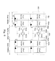
- Fig. 9 shows schematically a conventional AMOLED display device 900.
- the AMOLED display device 900 includes a plurality of regularly-spaced emission pixels 952 (each represented by a dashed square) positioned in a display area 950 and a plurality of pixel circuits 954 (each represented by a solid square).
- Each pixel circuit 954 is positioned directly below and electrically coupled a respective emission pixel 952 for controlling the current through the respective emission pixel 952 in response to an applied data signal.
- the pixel circuits 954 in each column arc coupled to a respective data line 910.
- the pixel circuits 954 in each row are coupled to a respective scan line 920.
- the AMOLED display device 900 further includes a vertical shift registers (VSR) 940 and a plurality of buffer circuits 930.
- VSR 940 comprises a plurality of stages. Each VSR stage is configured to output a scan signal to a respective buffer circuit 930 to drive a respective row of pixel circuits 954.
- the plurality of VSR stages are connected to each other in series such that successive rows of pixel circuits are sequentially driven in a row by row fashion in response to a clock signal.
- Fig. 10 is an equivalent circuit diagram for one pixel row of the AMOLED display device 900 shown in Fig. 9 .
- a complimentary metal oxide semiconductor (CMOS) VSR stage 40 outputs a scan signal to a buffer circuit 30, which drives a panel loading 50 of a corresponding row of pixels.
- the panel loading 50 is represented by an equivalent RC circuit.
- the buffer circuit 30 performs wave shaping to the scan signal so that it can sufficiently cope with the panel loading 50.
- the buffer circuit 30 may comprise several logic inverters 32 connected to each other in series. Each logic inverter 32 comprises a TFT having a channel width along the row direction. The driving ability of a buffer circuit is determined largely by the channel width-to-length-ratio (W/L) of the TFT.
- W/L channel width-to-length-ratio
- the channel width of the TFT in one logic inverter is greater than the channel width of the TFT in a previous logic inverter in the series.
- the driving ability of the buffer circuit is enhanced.
- the width of the buffer circuit 30 may be quite wide.
- Fig. 11 shows schematically the layout of a conventional AMOLED display device 10.
- the AMOLED display device 10 includes a display area 51 where the emission pixels and pixel circuits are disposed.
- a VSR 41 and buffer circuits 31 may be disposed at the left or right peripheral edge of the display area. Because the width W1 of the buffer circuits 31 needs to be sufficiently wide as described above, the total border width W of the display device 10 may be quite wide.
- the active matrix electroluminescent display device includes an emission layer and a circuit layer.
- the emission layer includes a plurality of regularly-spaced emission pixels disposed in a row.
- the circuit layer is disposed under the emission layer and includes a plurality of pixel circuits. Each pixel circuit is electrically coupled to a respective emission pixel for controlling the current through the respective emission pixel in response to an applied data signal.
- the plurality of pixel circuits is spatially arranged into a plurality of groups with each group including one or more adjacent pixel circuits. Any two neighboring groups of adjacent pixel circuits are separated by a space therebetween.
- the circuit layer further includes a plurality of buffer circuits connected to each other in series. Each buffer circuit is configured to drive a respective group of adjacent pixel circuits in response to a scan signal. At least one buffer circuit is positioned in a respective space between two neighboring groups of adjacent pixel circuits.
- the number of pixel circuits in each group is the same for all groups.
- each buffer circuit includes one or more logic inverters.
- Each logic inverter comprises a thin film transistor (TFT) having a channel width along the row direction.
- TFT thin film transistor
- the one or more logic inverters in each buffer circuit includes two ore more logic inverters connected to each other in series, wherein a TFT of any one but the first logic inverter has a channel width that is greater than a channel width of a TFT of a previous logic inverter.
- each pixel circuit comprises a TFT.
- the present invention relates to an active matrix electroluminescent display device.
- the active matrix electroluminescent display device includes an emission layer and a circuit layer.
- the emission layer includes a plurality of regularly-spaced emission pixels positioned in a display area in a form of a matrix with a plurality of rows and a plurality of columns.
- the circuit layer is disposed under the emission layer and includes a plurality of pixel circuits. Each pixel circuit is electrically coupled to a respective emission pixel for controlling the current through the respective emission pixel in response to an applied data signal.
- the plurality of pixel circuits is spatially arranged in a plurality of zones.
- Each zone includes one or more columns of pixel circuits and has an area with a width in the row direction that is narrower than a width of an area occupied by corresponding one or more columns of emission pixels in the emission layer such that any two neighboring zones are separated by a space therebetween.
- the circuit layer further includes a plurality of buffer circuitries. Each buffer circuitry is electrically coupled to a respective row of pixel circuits and includes a plurality of buffer circuits connected to each other in series. Each buffer circuit is configured to drive one or more adjacent pixel circuits in a respective zone in the respective row in response to a scan signal. At least one buffer circuit is positioned in a respective space between two neighboring zones.
- the active matrix electroluminescent display device further includes a shift register.
- the shift register includes a plurality of stages. Each stage is configured to output a scan signal to a respective buffer circuitry in response to a clock signal.
- the plurality of stages of the shift register is connected to each other in series so that successive rows of pixel circuits are sequentially driven in a row-by-row fashion.
- the shift register is disposed at a peripheral edge of the display area in the column direction.
- the plurality of stages of the shift register is disposed at two opposite peripheral edges of the display area in the column direction.
- each stage of the shift register comprises a thin film complementary metal oxide semiconductor (CMOS) transistor.
- CMOS complementary metal oxide semiconductor
- each buffer circuit in each buffer circuitry comprises at least one TFT having a channel width along the row direction.
- each pixel circuit comprises at least one TFT.
- the present invention relates to a method of driving an active matrix electroluminescent display device.
- the active matrix electroluminescent display device includes an emission layer and a circuit layer.
- the emission layer includes a plurality of regularly-spaced emission pixels disposed in a display area in a form of a matrix with a plurality of rows and a plurality of columns.
- the circuit layer is disposed under the emission layer and includes a plurality of pixel circuits. Each pixel circuit is electrically coupled to a respective emission pixel for controlling the current through the respective emission pixel in response to an applied data signal.
- the plurality of pixel circuits in each row is arranged into a plurality of groups with each group including one or more adjacent pixel circuits.
- the method includes the step of providing a clock signal to a shift register.
- the shift register includes a plurality of stages. Each stage corresponds to a respective row of pixel circuits and is configured to output a scan signal to a respective buffer circuitry in response to the clock signal.
- the respective buffer circuitry includes a plurality of buffer circuits connected to each other in series. Each buffer circuit is configured to drive a respective group of adjacent pixel circuits in the respective row.
- the plurality of stages of the shift register is connected to each other in series such that successive rows of pixel circuits are sequentially driven in a row-by-row fashion.
- At least one buffer circuit in each buffer circuitry is disposed in a space between two neighboring groups of adjacent pixel circuits in the respective row.
- the shift register is disposed at a peripheral edge of the display area in the column direction.
- the plurality of stages of the shift register is disposed at two opposite peripheral edges of the display area in the column direction.
- this invention in one aspect, relates to an electroluminescent display device, more particularly to an AMOLED display device with a slim border.
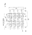
- Fig. 1 shows schematically an AMOLED display device 100 according to one embodiment of the present invention.
- the AMOLED display device 100 comprises an emission layer and a circuit layer.
- the emission layer comprises a plurality of regularly spaced emission pixels 154 (each represented by a dashed square) disposed in a display area 150 in a form of a matrix with a plurality of rows and a plurality of columns.
- the circuit layer is disposed under the emission layer and comprises a plurality of pixel circuits 152 (each represented by a solid rectangle), those skill in the art known that the circuit layer disposed behind emission layer for prevent reducing aperture ratio.
- Each pixel circuit is electrically coupled to a respective emission pixel 154 for controlling the current through the respective emission pixel 154 in response to an applied data signal.
- the pixel circuits in each column are coupled to a respective data line 110.
- the plurality of pixel circuits 152 in each row is spatially arranged into a plurality of groups with each group including one or more adjacent pixel circuits 152.
- each group includes two adjacent pixel circuits 152.
- Each group of adjacent pixel circuits 152 occupies an area 156 (dark shaded area) having a width in the row direction that is narrower than the area 158 (light shaded area) occupied by the corresponding emission pixels, so that any two neighboring groups of adjacent pixel circuits 152 are separated by a space 160 therebetween.
- the AMOLED display device 100 further includes a plurality of buffer circuitries 130.
- Each buffer circuitry 130 is configured to receive a scan signal from a shift register 140 and is electrically coupled to a respective row of pixel circuits 152 through a scan line 120.
- Each buffer circuitry 130 includes a plurality of buffer circuits 132/134/136 connected to each other in series. Each buffer circuit 132/134/136 is configured to drive a respective group of adjacent pixel circuits 152 in the respective row in response to a scan signal.
- each buffer circuit 132/134/136 since each buffer circuit 132/134/136 only drives one group of adjacent pixel circuits as compared of an entire row of pixel circuits in a conventional AMOLED display device, each buffer circuit 132/134/136 may be made with a relatively narrow channel width in the row direction and may be positioned in a spaces 160 between two neighboring groups of adjacent pixel circuits 152 in the display area 150. Accordingly, the AMOLED display device 100 can be made with a relatively slim border compared to a conventional AMOLED display device.
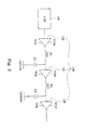
- Fig. 2 shows an equivalent circuit diagram for one pixel row of the AMOLED display device 100 shown in Fig. 1 .
- R1 and C1 represent the equivalent circuit loading for the first group of pixel circuits
- R2 and C2 represent the equivalent circuit loading for the second group of pixel circuits, etc.
- the shift register 140 outputs a scan signal to the buffer circuitry 130.
- the first buffer circuit 132 of the buffer circuitry 130 drives the circuit loading of R1 and C1
- the second buffer circuit 134 of the buffer circuitry 130 drives the circuit loading of R2 and C2, etc.
- each buffer circuit 132/134/136 comprises one or more logic inverters.
- Each logic inverter comprises a TFT.
- Fig. 3 shows schematically a layout of an AMOLED display device 300 according to one embodiment of the present invention.
- the AMOLED display device 300 includes a display area 350.
- the display area 350 is divided into n vertical zones 356, where n is an integer greater than or equal to 2.
- Each zone 356 has an area with a width of D1 in the row direction and includes one or more columns of pixel circuits. Any two neighboring zones 356 are separated by a space 358 of width D3 in the row direction, in which a column of buffer circuits is disposed.
- a corresponding zone 352 has an area with a width of D2 in the row direction.
- Neighboring zones 352 are arranged next to each other without any space therebetween.
- a VSR 340a and 340b is disposed at the left and right peripheral edges of the display area 350 and is coupled to the buffer circuits disposed in the spaces 358 between neighboring zones 356 in the display area 350.
- the AMOLED display device 300 can be made with a relatively narrow border with a width W.
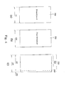
- Fig. 4 illustrates the relationship between the emission layer and the circuit layer for the AMOLED display device 300.
- Figs. 4a and 4b show a zone 356 in the circuit layer and a corresponding zone 352 in the emission layer, respectively.
- the zone 356 in the circuit layer and the zone 352 in the emission layer have a width of D1 and D2 respectively, D1 being less than D2.
- the zone 352 in the emission layer is overlaid on top of the zone 356 in the circuit layer as is the case in an AMOLED display device. While neighboring zones 352 in the emission layer are arranged right against each other without any space therebetween, neighboring zones 356 in the circuit layer are separated by a space 358 with a width of D3 as indicated in Fig. 4c .
- Fig. 5 shows schematically a layout of buffer circuits 334 in a space 358 between two neighboring zones 356.
- each buffer circuit 334 for driving a group of adjacent pixel circuits in the zone to the right of the space 358.
- each buffer circuit 334 comprises two logic inverters 334a and 334b connected to each other in series.
- each buffer circuit 334 may comprise more or fewer number of logic inverters connected to each other in series.
- Each logic inverter comprises a TFT having a channel width along the row direction. In one embodiment, any one but the first logic inverter has a channel width that is greater than a channel width of a TFT of a previous logic inverter.
- Fig. 6 shows schematically a layout of emission pixels, pixel circuits, and buffer circuits in a region in the vicinity of a space 658 between two neighboring zones 656a and 656b, according to one embodiment of the present invention.
- Emission pixels 652 (represented by dashed rectangles) in each row are arranged as a regular array.
- Pixel circuits 654 (represented by solid rectangles) in each row are arranged into groups with a space 658 between two neighboring groups.
- Each pixel circuit 654 occupies an area with a width T1 that is narrower than a width T2 of the area occupied by each emission pixel 652.
- Some emission pixels 652 are located in the space 658 between neighboring groups of pixel circuits 654.
- each row two emission pixels 652a and 652b are located in the space 658.
- One of those two emission pixels 652a is coupled to the pixel circuit 654a in the first zone 656a; the other one of the two emission pixels 652b is coupled to the pixel circuit 654b in the second zone 656b.
- a buffer circuit 634 is positioned in the space 658 between the first zone 656a and the second zone 656b and is configured to drive the pixel circuits in the second zone 656b in the corresponding row in response to a scan signal.
- each buffer circuit 634 comprises two logic inverters 634a and 634b.
- Fig. 7 shows a partial cross sectional view of a top emission type AMOLED display device 700 according to one embodiment of the present invention.
- the AMOLED display device 700 includes a circuit layer 720 formed on a substrate 710 such as glass, and an emission layer 730 formed on the circuit layer 720.
- the emission layer 730 includes a plurality of regularly spaced emission pixels 750.
- Each emission pixel 750 has a cathode 752, an anode 754, and an organic active layer 756 disposed between the cathode 752 and the anode 754. Neighboring emission pixels 750 are separated by a pixel define material 758.
- the circuit layer 720 includes a plurality of pixel circuits 760. Each pixel circuit 760 comprises a TFT.
- the TFT comprises a semiconductor layer 762, a gate electrode 764, a source/drain electrode 766, a dielectric layer 769 disposed between the gate electrode 764 and the source/drain electrode 766, and a gate insulator layer 768 disposed between the semiconductor layer 762 and the gate electrode 764.
- a flatten layer 790 is disposed between the circuit layer 720 and the emission layer 730.
- the plurality of pixel circuits 760 are arranged in a plurality of zones 782.
- a buffer circuit 770 is positioned in a space 780 between two neighboring zones 782.
- the buffer circuit 770 comprises two logic inverters 772a and 772b.
- the bottom emission type OLED the circuit layer disposed on the above side of the emission layer, so those skill in the art will disposed the circuit layer on the non-emission side of the emission layer for prevent blocking light transmitting.
- an AMOLED display device can be made with a relatively slim border.
- the display area of a 3.7" wide video graphic array (WVGA) with a resolution of 480 ⁇ 800 may be divided into 12 vertical zones. Each zone includes 40 columns of pixels.
- the panel loading for 480 pixels in each row has an equivalent RC value of about 9 k ⁇ and 80 pF, respectively.
- the panel loading for 40 pixels has an equivalent RC value of about 2 k ⁇ and 12 pF, respectively.
- a buffer circuit configured to drive 40 pixels can be positioned in a buffer area between neighboring zones having a width of about 22 ⁇ m. Consequently, the width of the panel border can be reduced from 1950 ⁇ m in a conventional AMOLED display device to about 1570 ⁇ m according one embodiment of the present invention.
Landscapes
- Engineering & Computer Science (AREA)
- Physics & Mathematics (AREA)
- Computer Hardware Design (AREA)
- General Physics & Mathematics (AREA)
- Theoretical Computer Science (AREA)
- Geometry (AREA)
- Microelectronics & Electronic Packaging (AREA)
- Electroluminescent Light Sources (AREA)
- Devices For Indicating Variable Information By Combining Individual Elements (AREA)
Applications Claiming Priority (1)
| Application Number | Priority Date | Filing Date | Title |
|---|---|---|---|
| US13/070,262 US20120242708A1 (en) | 2011-03-23 | 2011-03-23 | Active matrix electroluminescent display |
Publications (1)
| Publication Number | Publication Date |
|---|---|
| EP2503536A1 true EP2503536A1 (de) | 2012-09-26 |
Family
ID=44644873
Family Applications (1)
| Application Number | Title | Priority Date | Filing Date |
|---|---|---|---|
| EP11006463A Withdrawn EP2503536A1 (de) | 2011-03-23 | 2011-08-05 | Aktive Matrix-Elektrolumineszenzanzeige |
Country Status (4)
| Country | Link |
|---|---|
| US (1) | US20120242708A1 (de) |
| EP (1) | EP2503536A1 (de) |
| CN (1) | CN102436790A (de) |
| TW (1) | TW201239843A (de) |
Cited By (1)
| Publication number | Priority date | Publication date | Assignee | Title |
|---|---|---|---|---|
| EP2669884A3 (de) * | 2012-05-31 | 2014-11-19 | Samsung Display Co., Ltd. | Anzeigetafel |
Families Citing this family (13)
| Publication number | Priority date | Publication date | Assignee | Title |
|---|---|---|---|---|
| JP2015004945A (ja) * | 2013-02-04 | 2015-01-08 | ソニー株式会社 | 表示装置及びその駆動方法、並びに、制御パルス生成装置 |
| US9177513B2 (en) | 2013-05-22 | 2015-11-03 | Vizio, Inc | Electroluminescent display where each pixel can emit light of any EIA color index |
| CN104409041A (zh) * | 2014-12-02 | 2015-03-11 | 昆山工研院新型平板显示技术中心有限公司 | 有源有机发光显示器及其驱动电路 |
| CN104505050B (zh) * | 2014-12-31 | 2017-02-01 | 深圳市华星光电技术有限公司 | 用于氧化物半导体薄膜晶体管的扫描驱动电路 |
| CN105931606B (zh) * | 2016-05-27 | 2019-07-12 | 厦门天马微电子有限公司 | 栅极驱动结构和显示装置 |
| TWI709791B (zh) * | 2016-07-07 | 2020-11-11 | 日商半導體能源研究所股份有限公司 | 顯示裝置及電子裝置 |
| TWI643013B (zh) * | 2017-03-29 | 2018-12-01 | 友達光電股份有限公司 | 顯示器 |
| CN106898324B (zh) * | 2017-04-25 | 2019-09-17 | 京东方科技集团股份有限公司 | 一种显示面板及显示装置 |
| KR102507830B1 (ko) * | 2017-12-29 | 2023-03-07 | 엘지디스플레이 주식회사 | 디스플레이 장치 |
| KR102555212B1 (ko) * | 2017-12-29 | 2023-07-12 | 엘지디스플레이 주식회사 | 발광 표시 장치 |
| KR102555210B1 (ko) * | 2017-12-29 | 2023-07-12 | 엘지디스플레이 주식회사 | 발광 표시 장치 |
| TWI692665B (zh) * | 2018-08-10 | 2020-05-01 | 友達光電股份有限公司 | 顯示裝置 |
| CN110992912B (zh) * | 2019-12-27 | 2022-04-29 | 厦门天马微电子有限公司 | 一种阵列基板、显示面板及显示装置 |
Citations (4)
| Publication number | Priority date | Publication date | Assignee | Title |
|---|---|---|---|---|
| US5396262A (en) * | 1993-03-01 | 1995-03-07 | Wah-Iii Technology Corporation | Polysilicon gate bus with interspersed buffers for driving a row of pixels in an active matrix liquid crystal display |
| EP1065723A2 (de) * | 1999-06-28 | 2001-01-03 | Sel Semiconductor Energy Laboratory Co., Ltd. | Elektrolumineszente Anzeigevorrichtung und elektronische Vorrichtung |
| US20090121973A1 (en) * | 2007-11-08 | 2009-05-14 | Hyung-Soo Kim | Display device and method of fabricating the same |
| US20090201230A1 (en) * | 2006-06-30 | 2009-08-13 | Cambridge Display Technology Limited | Active Matrix Organic Electro-Optic Devices |
Family Cites Families (6)
| Publication number | Priority date | Publication date | Assignee | Title |
|---|---|---|---|---|
| TW468283B (en) * | 1999-10-12 | 2001-12-11 | Semiconductor Energy Lab | EL display device and a method of manufacturing the same |
| JP4194451B2 (ja) * | 2002-09-02 | 2008-12-10 | キヤノン株式会社 | 駆動回路及び表示装置及び情報表示装置 |
| KR100515305B1 (ko) * | 2003-10-29 | 2005-09-15 | 삼성에스디아이 주식회사 | 발광 표시 장치 및 그 표시 패널과 구동 방법 |
| GB0400209D0 (en) * | 2004-01-07 | 2004-02-11 | Koninkl Philips Electronics Nv | Light emitting display devices |
| US20060187175A1 (en) * | 2005-02-23 | 2006-08-24 | Wintek Corporation | Method of arranging embedded gate driver circuit for display panel |
| KR100898675B1 (ko) * | 2007-04-19 | 2009-05-22 | 삼성모바일디스플레이주식회사 | 유기 전계 발광 표시 장치, 이를 이용한 다기능 키패드용표시 장치 및 그 구동 방법 |
-
2011
- 2011-03-23 US US13/070,262 patent/US20120242708A1/en not_active Abandoned
- 2011-08-05 EP EP11006463A patent/EP2503536A1/de not_active Withdrawn
- 2011-11-18 TW TW100142373A patent/TW201239843A/zh unknown
- 2011-12-21 CN CN2011104422367A patent/CN102436790A/zh active Pending
Patent Citations (4)
| Publication number | Priority date | Publication date | Assignee | Title |
|---|---|---|---|---|
| US5396262A (en) * | 1993-03-01 | 1995-03-07 | Wah-Iii Technology Corporation | Polysilicon gate bus with interspersed buffers for driving a row of pixels in an active matrix liquid crystal display |
| EP1065723A2 (de) * | 1999-06-28 | 2001-01-03 | Sel Semiconductor Energy Laboratory Co., Ltd. | Elektrolumineszente Anzeigevorrichtung und elektronische Vorrichtung |
| US20090201230A1 (en) * | 2006-06-30 | 2009-08-13 | Cambridge Display Technology Limited | Active Matrix Organic Electro-Optic Devices |
| US20090121973A1 (en) * | 2007-11-08 | 2009-05-14 | Hyung-Soo Kim | Display device and method of fabricating the same |
Cited By (6)
| Publication number | Priority date | Publication date | Assignee | Title |
|---|---|---|---|---|
| EP2669884A3 (de) * | 2012-05-31 | 2014-11-19 | Samsung Display Co., Ltd. | Anzeigetafel |
| US9406266B2 (en) | 2012-05-31 | 2016-08-02 | Samsung Display Co., Ltd. | Display panel |
| US20160307517A1 (en) | 2012-05-31 | 2016-10-20 | Samsung Display Co., Ltd. | Display panel |
| EP3550552A3 (de) * | 2012-05-31 | 2019-11-20 | Samsung Display Co., Ltd. | Anzeigetafel |
| US10783833B2 (en) | 2012-05-31 | 2020-09-22 | Samsung Display Co., Ltd. | Display panel |
| US11282464B2 (en) | 2012-05-31 | 2022-03-22 | Samsung Display Co., Ltd. | Display panel |
Also Published As
| Publication number | Publication date |
|---|---|
| TW201239843A (en) | 2012-10-01 |
| US20120242708A1 (en) | 2012-09-27 |
| CN102436790A (zh) | 2012-05-02 |
Similar Documents
| Publication | Publication Date | Title |
|---|---|---|
| EP2503536A1 (de) | Aktive Matrix-Elektrolumineszenzanzeige | |
| US12249283B2 (en) | Display apparatus | |
| US8334859B2 (en) | Electroluminescent display and method of driving same | |
| US11355562B2 (en) | Display apparatus | |
| US10147767B2 (en) | Display device | |
| US20070152923A1 (en) | Light emitting display and method of driving thereof | |
| US12374290B2 (en) | Display panel and display device | |
| US12389770B2 (en) | Display panel and display device | |
| US10338424B2 (en) | Curved display apparatus | |
| US12499812B2 (en) | Display device and display panel | |
| CN115662331A (zh) | 显示基板及其驱动方法、显示装置 | |
| CN115472126A (zh) | 像素电路及其驱动方法、显示基板和显示装置 | |
| US9792854B2 (en) | Display device | |
| US20240290797A1 (en) | Display Panel and Display Device | |
| KR102868778B1 (ko) | 디스플레이 모듈 | |
| JP2008268437A (ja) | 有機el表示装置 | |
| US20230117897A1 (en) | Display module | |
| JP2004126106A (ja) | エレクトロルミネッセンス表示装置 | |
| JP2005122183A (ja) | エレクトロルミネセンス表示装置 | |
| US8094110B2 (en) | Active matrix display device | |
| CN118397971A (zh) | 显示设备 | |
| CN116249398A (zh) | 发光显示装置及其制造方法 | |
| KR20160074801A (ko) | 표시패널 및 이를 구비하는 유기 전계발광 표시장치 | |
| JP5085011B2 (ja) | アクティブマトリクス型表示装置 | |
| KR100538331B1 (ko) | 일렉트로 루미네센스 표시장치 |
Legal Events
| Date | Code | Title | Description |
|---|---|---|---|
| PUAI | Public reference made under article 153(3) epc to a published international application that has entered the european phase |
Free format text: ORIGINAL CODE: 0009012 |
|
| 17P | Request for examination filed |
Effective date: 20111021 |
|
| AK | Designated contracting states |
Kind code of ref document: A1 Designated state(s): AL AT BE BG CH CY CZ DE DK EE ES FI FR GB GR HR HU IE IS IT LI LT LU LV MC MK MT NL NO PL PT RO RS SE SI SK SM TR |
|
| AX | Request for extension of the european patent |
Extension state: BA ME |
|
| 17Q | First examination report despatched |
Effective date: 20150302 |
|
| STAA | Information on the status of an ep patent application or granted ep patent |
Free format text: STATUS: THE APPLICATION IS DEEMED TO BE WITHDRAWN |
|
| 18D | Application deemed to be withdrawn |
Effective date: 20150714 |