EP2500805A2 - Touch panel and touch screen having the same - Google Patents
Touch panel and touch screen having the same Download PDFInfo
- Publication number
- EP2500805A2 EP2500805A2 EP12159436A EP12159436A EP2500805A2 EP 2500805 A2 EP2500805 A2 EP 2500805A2 EP 12159436 A EP12159436 A EP 12159436A EP 12159436 A EP12159436 A EP 12159436A EP 2500805 A2 EP2500805 A2 EP 2500805A2
- Authority
- EP
- European Patent Office
- Prior art keywords
- conductive layer
- layer
- touch panel
- capacitive
- transparent substrate
- Prior art date
- Legal status (The legal status is an assumption and is not a legal conclusion. Google has not performed a legal analysis and makes no representation as to the accuracy of the status listed.)
- Granted
Links
Images

Classifications
-
- G—PHYSICS
- G06—COMPUTING; CALCULATING OR COUNTING
- G06F—ELECTRIC DIGITAL DATA PROCESSING
- G06F3/00—Input arrangements for transferring data to be processed into a form capable of being handled by the computer; Output arrangements for transferring data from processing unit to output unit, e.g. interface arrangements
- G06F3/01—Input arrangements or combined input and output arrangements for interaction between user and computer
- G06F3/03—Arrangements for converting the position or the displacement of a member into a coded form
- G06F3/041—Digitisers, e.g. for touch screens or touch pads, characterised by the transducing means
- G06F3/044—Digitisers, e.g. for touch screens or touch pads, characterised by the transducing means by capacitive means
- G06F3/0443—Digitisers, e.g. for touch screens or touch pads, characterised by the transducing means by capacitive means using a single layer of sensing electrodes
-
- G—PHYSICS
- G06—COMPUTING; CALCULATING OR COUNTING
- G06F—ELECTRIC DIGITAL DATA PROCESSING
- G06F3/00—Input arrangements for transferring data to be processed into a form capable of being handled by the computer; Output arrangements for transferring data from processing unit to output unit, e.g. interface arrangements
- G06F3/01—Input arrangements or combined input and output arrangements for interaction between user and computer
- G06F3/03—Arrangements for converting the position or the displacement of a member into a coded form
- G06F3/041—Digitisers, e.g. for touch screens or touch pads, characterised by the transducing means
- G06F3/044—Digitisers, e.g. for touch screens or touch pads, characterised by the transducing means by capacitive means
- G06F3/0445—Digitisers, e.g. for touch screens or touch pads, characterised by the transducing means by capacitive means using two or more layers of sensing electrodes, e.g. using two layers of electrodes separated by a dielectric layer
-
- G—PHYSICS
- G06—COMPUTING; CALCULATING OR COUNTING
- G06F—ELECTRIC DIGITAL DATA PROCESSING
- G06F3/00—Input arrangements for transferring data to be processed into a form capable of being handled by the computer; Output arrangements for transferring data from processing unit to output unit, e.g. interface arrangements
- G06F3/01—Input arrangements or combined input and output arrangements for interaction between user and computer
- G06F3/03—Arrangements for converting the position or the displacement of a member into a coded form
- G06F3/041—Digitisers, e.g. for touch screens or touch pads, characterised by the transducing means
- G06F3/044—Digitisers, e.g. for touch screens or touch pads, characterised by the transducing means by capacitive means
- G06F3/0446—Digitisers, e.g. for touch screens or touch pads, characterised by the transducing means by capacitive means using a grid-like structure of electrodes in at least two directions, e.g. using row and column electrodes
-
- G—PHYSICS
- G06—COMPUTING; CALCULATING OR COUNTING
- G06F—ELECTRIC DIGITAL DATA PROCESSING
- G06F2203/00—Indexing scheme relating to G06F3/00 - G06F3/048
- G06F2203/041—Indexing scheme relating to G06F3/041 - G06F3/045
- G06F2203/04103—Manufacturing, i.e. details related to manufacturing processes specially suited for touch sensitive devices
-
- G—PHYSICS
- G06—COMPUTING; CALCULATING OR COUNTING
- G06F—ELECTRIC DIGITAL DATA PROCESSING
- G06F2203/00—Indexing scheme relating to G06F3/00 - G06F3/048
- G06F2203/041—Indexing scheme relating to G06F3/041 - G06F3/045
- G06F2203/04111—Cross over in capacitive digitiser, i.e. details of structures for connecting electrodes of the sensing pattern where the connections cross each other, e.g. bridge structures comprising an insulating layer, or vias through substrate
Definitions
- the following description relates to a touch panel, and more particularly to a touch panel that supports various input methods and a touch screen having the same.
- a touch screen refers to a device in which an input detection means is integrated into a display means.
- a touch screen may include a display unit, such as an LCD (Liquid Crystal Display), as well as a touch panel provided on such a display unit.
- LCD Liquid Crystal Display
- Such a touch screen receives a user's input through a screen touch.
- the touch screen may recognize a character or a position displayed on a screen that is touched by the finger tip of a user or the tip of an object such as a stylus, without the use of a mechanical keypad.
- touch screens are widely used as an information display device in a place frequently visited by people, for example, as in a public place like a subway station, a department store or a bank, due to the simplicity of operation of such a device.
- the touch screens are not only frequently applied to counter terminals in various stores, but also widely employed recently in portable terminals, such as mobile phones, DMB (Digital Multimedia Broadcasting) receivers, and car navigation systems.
- DMB Digital Multimedia Broadcasting
- the touch panels are classified into a resistive overlay type, a capacitive type, a surface acoustic wave type, an infrared beam type, etc. At present, capacitive-type touch panels are most widely used.
- capacitive-type touch screens have a problem in that they are operated only when they are touched by a conductor, such as a human finger.
- Conventional capacitive-type touch screens do not sense the input when they are touched by a nonconductor object. This may cause inconveniences to a user due to the limited methods of input.
- the capacitive-type touch panel may include a first transparent substrate, a first conductive layer positioned on the first transparent substrate, a sensor layer having a second conductive layer spaced from the first conductive layer by a spacer, and a second transparent substrate positioned on the sensor layer.
- the first conductive layer and the second conductive layer may be transparent.
- the first conductive layer may be configured to have a preset reference electric potential
- the second conductive layer may be configured to sense a touch produced by a non-conductive user input object.
- An air layer may be disposed between the first conductive layer and the second conductive layer, and a space provided in the air layer may be sealed.
- the second transparent substrate may be attached to the sensor layer through an adhesive member.
- the touch panel may include a film positioned between the sensor layer and the first conductive layer.
- the film may be disposed between an air layer formed by the spacer and the sensor layer.
- the first conductive layer may have a uniform thickness and a flat surface.
- the first conductive layer may be formed with ITO, PEDOT or the like.
- the second conductive layer may include a plurality of first electrode lines and a plurality of second electrode lines.
- the plurality of electrodes and the plurality of second electrode lines may be spaced apart from each other via a bridge layer comprising an insulative dielectric material.
- a touch screen with a capacitive-type touch panel may include a display unit having a plurality of pixels for displaying images through the pixels, and a capacitive-type touch panel attached to the display unit through an adhesive member.
- the capacitive-type touch panel of such a touch screen may include a first transparent substrate, a first conductive layer positioned on the first transparent substrate, a sensor layer having a second conductive layer spaced from the first conductive layer by a spacer, and a second transparent substrate positioned on the sensor layer.
- the first conductive layer and the second conductive layer may be transparent.
- the first conductive layer may be connected to a ground, and a touch detection signal with a preset voltage wave form may be applied to the second conductive layer.
- the touch screen may also include a film positioned between the sensor layer and the first conductive layer.
- the film may be positioned between an air layer formed by the spacer and the sensor layer.
- the second conductive layer may include a plurality of first electrode lines and a plurality of second electrode lines.
- the plurality of electrodes and the plurality of second electrode lines may be spaced apart from each other via a bridge layer formed from an insulative dielectric material.
- a method of producing a touch screen may involve attaching a touch panel to a display unit, in which the touch panel includes a first transparent substrate, a first conductive layer, a spacer layer, a sensor layer having a second conductive layer, a second transparent substrate, stacked in that order.
- the first conductive layer and the second conductive layer of the touch panel may be transparent.
- the touch panel may be attached to the display unit via an adhesive member provided between a bottom side of the first transparent substrate and the display unit.
- the first conductive layer may be formed on the first transparent substrate via a vacuum deposition process.
- FIG. 1 illustrates a structure of an example of a touch panel.
- the touch panel 100 may include a first transparent substrate 110, a first conductive layer 120, a film 140, a sensor layer 150, and a second transparent substrate 170.
- the first transparent substrate 110 may form a base part of the touch panel 100, and may have a rectangular plate shape.
- the first transparent substrate 110 may be formed from an insulative material transparent to visible light. Examples of such an insulative material include glass, polyethylene terephthalate (PET), polycarbonate (PC), polyethylene naphthalate (PEN), polyphenylene sulfide (PPS), polyethersulfone (PES) and the like.
- the first conducive layer 120 may be laminated on the top of the first transparent substrate 110. That is, the first transparent substrate 110 may function as a support to the first conductive layer 120.
- the first conductive layer 120 may have a flat surface that is not provided with any pattern.
- the first conductive layer 120 may have a uniform thickness entirely.
- the first conductive layer 120 may have a preset reference electric potential (or voltage). For example, in a state in which it is connected to a ground and the touch panel 100 is being operated, the first conductive layer 120 may have a ground electric potential.
- the first conductive layer 120 may be referred to as a metallic layer, and it may be formed from a conductive material transparent to visible light.
- the first conductive layer 120 may be formed from a process for forming a conductive film through a vacuum deposition process. Examples of such a vacuum deposition process include electron beam deposition, sputtering and the like.
- the film 140 may be positioned on the top of the first conductive layer 120, and may function as a support to the sensor layer 150.
- the film 140 may also be spaced apart from the first conductive layer 120 by a spacer 130, and an air layer may be positioned between the film 140 and the first conductive layer 120.
- the space 135 between the film 140 and the first conductive layer 120 may be sealed.
- the film 140 may be formed from an insulative material transparent to visible light. Examples of such an insulative material include PET, PC, PEN, PES and the like.
- the spacer 130 may be laminated on the top of the first conductive layer 120 or around the bottom of the film 140 and may have a substantially rectangular strip shape.
- the spacer 130 may be formed in a single body or in a plurality of parts spaced apart from each other.
- an adhesive member such as an adhesive, a sealant member, a spherical, cylindrical or polyhedral strength member, or a combination thereof may be used as the spacer 130.
- a conventional curable material such as a UV-curable material, may be employed as the adhesive member
- a conductive polymer, such as polyacetylene may be employed as the strength member.
- the spacer 130 is laminated on the first conductive layer 120 in the present example
- the first conductive layer 120 may be laminated only on an area of the top of the first transparent substrate 110 surrounded by the spacer 130 in another example of touch panel. In such a touch panel, the spacer 130 may be directly laminated on the top of the first transparent substrate 110.
- the spacer 130 may perform a function of supporting the film 140 on the top of the first transparent substrate 110 to be spaced apart from the first transparent substrate 110. It may also perform a function of adhering the first transparent substrate 110 and the film 140 to one another.
- the sensor layer 150 may be laminated on the top of the film 140, in which the sensor layer 150 may include a second conductive layer 152 and a plurality of connection terminals 158.
- the sensor layer 150 may be provided with a plurality of sensors to determine a position touched by the tip of a human finger or the tip of any other object on the surface of the second transparent substrate 170.
- the second conductive layer 152 may have a preset pattern.
- the second conductive layer 152 may have various patterns, such as a lattice pattern with straight lines, and a diamond pattern. Such a lattice pattern is described below.
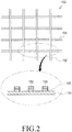
- FIG. 2 illustrates an example pattern of the second conductive layer 152.
- the second conductive layer 152 may include a plurality of first electrode lines 154 and a plurality of second electrode lines 156.
- the first electrode lines 154 may extend in a first direction (for example, x-axis or horizontal direction), and may be spaced at regular or irregular intervals from each other along a second direction (for example, ⁇ -axis or vertical direction) that lies at right angles to the first direction.
- a first direction for example, x-axis or horizontal direction
- a second direction for example, ⁇ -axis or vertical direction
- the second electrode lines 156 may extend in the second direction, and may be spaced at regular or irregular intervals from each other along the first direction.
- a bridge layer 155 may be interposed between the first and second electrode lines 154 and 156 at each of the crossing points of the first and second electrode lines 154 and 156.
- the bridge layer 155 may consist of bridge units, each of which may be positioned at one of the crossing points of the first and second electrode lines 154 and 156.
- the bridge layer 155 may be formed from an insulative dielectric material, such as SiO 2 .
- the second electrode layer 152 may be formed from a conductive material transparent to visible light.
- a conductive material include indium tin oxide (ITO), poly(3,4-ethylenedioxythiophene) (PEDOT) and the like.
- the second electrode layer 152 may be formed by forming a thin film through a vacuum deposition process and then patterning the thin film through a lithography process. Examples of such a vacuum deposition process include electron beam deposition, sputtering and the like.
- connection terminals 158 for applying voltage (or current) to the second conductive layer 152 can be laminated on the top of the film 140 to be positioned outside of the second conductive layer 152. That is, in order to facilitate access to the connection terminals 158 from the outside, the connection terminals 158 can be arranged outside of the second conductive layer 152 (i.e., on a marginal area of the film 140).
- connection terminals 158 may be electrically connected with the second conductive layer 152 through connection lines (not shown), in which the second connection terminals 158 and the connection lines may be formed through a single process or through separate processes.
- the connection terminals 158 may be formed from a material that is the same with the material of the second conductive layer 152.
- the connection terminals 158 may be formed from a material that is different from the material that forms the second conductive layer 152.
- the connection terminals 158 may be formed with an opaque conductive material, such as Ag.
- the connection terminals 158 may be electrically connected with a flexible printed circuit board (FPCB) which is provided with a controller or the like.
- FPCB flexible printed circuit board
- a preset wave-formed voltage i.e., a touch detection signal
- a touch sensing signal with a changed voltage wave form may be produced due to the change of the capacitance between the second conductive layer 152 and the user input object.
- the capacitance is referred to as first capacitance.
- the controller may analyze the touch sensing signal to determine whether the user input object touched or not touched the second transparent substrate 170, and to determine the touch position.
- the touch panel may be provided with an additional second capacitance between the second conductive layer 152 and the first conductive layer 120; the second capacitance may allow the determination of the touch position as described above even when the user input object is not conductive.
- the touch panel may sense a push pressure of the user input object, such as a finger, a stylus or the like.
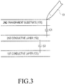
- FIG. 3 illustrates a method of detecting a touch position of the touch panel 100.
- FIG. 3 only the first and second conductive layers 120 and 150, and the second transparent substrate 170 are shown among the components of the touch panel 100.
- the first capacitance C1 between the second conductive layer 152 and the user input object 10 might not be produced or changed before and after the touch.
- the second capacitance C2 between the second conductive layer 152 and the first conductive layer 120 is changed before and after the touch. That is, as the second conductive layer 152 is bent toward the first conductive layer 120 due to the push by the user input object 10, the space between the second conductive layer 152 and the first conductive layer 120 is locally changed, which causes the change of the second capacitance C2. Accordingly, the touch panel 100 can determine whether an input is attempted or not and can even determine the input position where the input was attempted; this occurs even if a non-conductive device is used by the user as the input object 10.
- the second transparent substrate 170 may be attached to the top of the second conductive layer 152 using an adhesive member 160.
- the top side of the second transparent substrate 170 may be exposed to the outside to form at least a part of the front surface of the touch panel 100.
- the second transparent substrate 170 may be formed with an insulative material that is transparent to visible light. Examples of such an insulative material include glass, polycarbonate, polyethylene terephthalate and the like.
- the adhesive member 160 may be formed from an insulative material that is transparent to visible light.
- An optical clear adhesive (OCA) tape, an adhesive (or a sticking agent), a UV-curable resin or the like, which is transparent to visible light, can be used as the adhesive member 160.
- OCA tape is a double-sided adhesive tape, and is typically formed from acryl, silicone or the like.
- the sensor layer 150 may be laminated on the top of the film 140 in this example, the sensor layer 150 may be laminated on the bottom of the film 140 in another example.
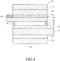
- FIG. 4 illustrates an example of a touch screen.
- the touch screen shown in FIG. 4 may include a touch panel 100 such as the one shown in FIG. 1 . Duplicated descriptions concerning the touch panel 100 will be omitted.
- the touch screen 200 may include a display unit 210, a touch panel 100 and a second adhesive member 220.
- the display unit 210 may include a plurality of pixels to display images through the pixels.
- An LCD Liquid Crystal Display
- OLED Organic Light Emitting Diodes
- An LCD may display images in accordance with the control of a controller (not shown).
- a conventional LCD may include: a liquid crystal display panel for displaying images, the liquid crystal display panel including a liquid crystal layer; and a BLU (Back Light Unit) for providing light to the liquid crystal display panel.
- the liquid crystal display panel may include upper and lower glass substrates arranged above and below the liquid crystal layer to control the arrangements of liquid crystal molecules.
- the lower glass substrate may include thin film transistors and pixel electrodes, and the upper grass substrate may include common electrodes.
- the liquid crystal panel may further include upper and lower polarization plates arranged above and below the liquid crystal layer to linearly polarize light as being input. The polarization directions of the upper and lower polarization plates may cross each other at a right angle.
- the touch panel 100 may be attached (i.e., adhered) to the display unit through a second adhesive member 220. That is, the bottom side of the touch panel 100 (i.e., the bottom side of the first transparent substrate 110) may be attached to the top of the display unit 210 through the second adhesive member 220.
- the bottom side of the second transparent substrate 170 may be antireflection (AR)-coated, in which the AR coating layer formed thereby may include an Nb 2 O 5 layer and a SiO 2 layer.
- AR antireflection
- the color difference value a* may be not more than 1.5
- the color difference value b* may be not more than 1.5
- the transmittance may be not less than 91%
- the reflectance may be 5% to 10 %.
- the touch panel 100 may have a transmittance of not less than 88%.
- the a* and b* are components of the CIE coordinate system for indicating colors, in which as the values thereof go further away from zero, stronger colors are indicated.
- a light interruption layer for interrupting visible light may be laminated on the bottom side of the second transparent substrate 170 along a marginal area surrounding the central area included in an effective display region in order to prevent the marginal area from being revealed to the outside.
- the light interrupting layer may be formed through a black ink printing process or the like.
- the inventive touch panel and touch screen having the same are useful in that even if a user input object is non-conductive, the touch panel and touch screen can sense a push pressure applied by the non-conductive user input object through a second capacitance providing unit; thereby, the touch panel and touch screen can determine whether an input is attempted or not attempted and determine the input position where the input was attempted.
- the touch panel and touch screen are input devices in which information can be freely input through a conductive or non-conductive user input object.
- first layer is referred to as being "on" a second layer or “on” a substrate, it may not only refer to a case where the first layer is formed directly on the second layer or the substrate but may also refer to a case where a third layer exists between the first layer and the second layer or the substrate.
Abstract
Description
- The following description relates to a touch panel, and more particularly to a touch panel that supports various input methods and a touch screen having the same.
- In general, a touch screen refers to a device in which an input detection means is integrated into a display means. A touch screen may include a display unit, such as an LCD (Liquid Crystal Display), as well as a touch panel provided on such a display unit.
- Such a touch screen receives a user's input through a screen touch. For example, the touch screen may recognize a character or a position displayed on a screen that is touched by the finger tip of a user or the tip of an object such as a stylus, without the use of a mechanical keypad.
- Although not excellent in precision, touch screens are widely used as an information display device in a place frequently visited by people, for example, as in a public place like a subway station, a department store or a bank, due to the simplicity of operation of such a device. The touch screens are not only frequently applied to counter terminals in various stores, but also widely employed recently in portable terminals, such as mobile phones, DMB (Digital Multimedia Broadcasting) receivers, and car navigation systems.
- The touch panels (or touch screens) are classified into a resistive overlay type, a capacitive type, a surface acoustic wave type, an infrared beam type, etc. At present, capacitive-type touch panels are most widely used.
- However, conventional capacitive-type touch screens have a problem in that they are operated only when they are touched by a conductor, such as a human finger. Conventional capacitive-type touch screens do not sense the input when they are touched by a nonconductor object. This may cause inconveniences to a user due to the limited methods of input.
- Summary of the Invention In one general aspect, there is provided a capacitive-type touch panel. The capacitive-type touch panel may include a first transparent substrate, a first conductive layer positioned on the first transparent substrate, a sensor layer having a second conductive layer spaced from the first conductive layer by a spacer, and a second transparent substrate positioned on the sensor layer. The first conductive layer and the second conductive layer may be transparent.
- The first conductive layer may be configured to have a preset reference electric potential, and the second conductive layer may be configured to sense a touch produced by a non-conductive user input object.
- An air layer may be disposed between the first conductive layer and the second conductive layer, and a space provided in the air layer may be sealed.
- The second transparent substrate may be attached to the sensor layer through an adhesive member.
- In addition, the touch panel may include a film positioned between the sensor layer and the first conductive layer. The film may be disposed between an air layer formed by the spacer and the sensor layer. The first conductive layer may have a uniform thickness and a flat surface. The first conductive layer may be formed with ITO, PEDOT or the like.
- In addition, the second conductive layer may include a plurality of first electrode lines and a plurality of second electrode lines. The plurality of electrodes and the plurality of second electrode lines may be spaced apart from each other via a bridge layer comprising an insulative dielectric material.
- In another aspect, there is provided a touch screen with a capacitive-type touch panel. The touch screen may include a display unit having a plurality of pixels for displaying images through the pixels, and a capacitive-type touch panel attached to the display unit through an adhesive member.
- The capacitive-type touch panel of such a touch screen may include a first transparent substrate, a first conductive layer positioned on the first transparent substrate, a sensor layer having a second conductive layer spaced from the first conductive layer by a spacer, and a second transparent substrate positioned on the sensor layer. The first conductive layer and the second conductive layer may be transparent.
- The first conductive layer may be connected to a ground, and a touch detection signal with a preset voltage wave form may be applied to the second conductive layer.
- The touch screen may also include a film positioned between the sensor layer and the first conductive layer. The film may be positioned between an air layer formed by the spacer and the sensor layer.
- In addition, the second conductive layer may include a plurality of first electrode lines and a plurality of second electrode lines. The plurality of electrodes and the plurality of second electrode lines may be spaced apart from each other via a bridge layer formed from an insulative dielectric material.
- In yet another aspect, there is provided a method of producing a touch screen. The method may involve attaching a touch panel to a display unit, in which the touch panel includes a first transparent substrate, a first conductive layer, a spacer layer, a sensor layer having a second conductive layer, a second transparent substrate, stacked in that order. The first conductive layer and the second conductive layer of the touch panel may be transparent.
- The touch panel may be attached to the display unit via an adhesive member provided between a bottom side of the first transparent substrate and the display unit. The first conductive layer may be formed on the first transparent substrate via a vacuum deposition process.
- Other features and aspects may be apparent from the following detailed description, drawings, and claims.
-
-
FIG. 1 is a schematic view illustrating a structure of one example of touch panel. -
FIG. 2 is a schematic view illustrating an example of pattern of a second conductive layer. -
FIG. 3 is a schematic view illustrating an example of a method for detecting a touched position on a touch panel. -
FIG. 4 is a schematic view illustrating a structure of one example of a touch screen. - Throughout the drawings and the detailed description, unless otherwise described, the same drawing reference numerals will be understood to refer to the same elements, features, and structures. The relative size and depiction of these elements may be exaggerated for clarity, illustration, and convenience.
- The following detailed description is provided to assist the reader in gaining a comprehensive understanding of the methods, apparatuses, and/or systems described herein. Accordingly, various changes, modifications, and equivalents of the systems, apparatuses and/or methods described herein will be suggested to those of ordinary skill in the art.
- Further, various specific definitions found in the following description are provided only to help general understanding of the present disclosure, and it is apparent to those skilled in the art that the described devices and methods can be implemented without such definitions. In addition, in the following description, a detailed description of known functions and configurations incorporated herein will be omitted when it may make the subject matter of the present disclosure rather unclear.
-
FIG. 1 illustrates a structure of an example of a touch panel. Thetouch panel 100 may include a firsttransparent substrate 110, a firstconductive layer 120, afilm 140, asensor layer 150, and a secondtransparent substrate 170. - The first
transparent substrate 110 may form a base part of thetouch panel 100, and may have a rectangular plate shape. The firsttransparent substrate 110 may be formed from an insulative material transparent to visible light. Examples of such an insulative material include glass, polyethylene terephthalate (PET), polycarbonate (PC), polyethylene naphthalate (PEN), polyphenylene sulfide (PPS), polyethersulfone (PES) and the like. - The first
conducive layer 120 may be laminated on the top of the firsttransparent substrate 110. That is, the firsttransparent substrate 110 may function as a support to the firstconductive layer 120. The firstconductive layer 120 may have a flat surface that is not provided with any pattern. The firstconductive layer 120 may have a uniform thickness entirely. The firstconductive layer 120 may have a preset reference electric potential (or voltage). For example, in a state in which it is connected to a ground and thetouch panel 100 is being operated, the firstconductive layer 120 may have a ground electric potential. The firstconductive layer 120 may be referred to as a metallic layer, and it may be formed from a conductive material transparent to visible light. Examples of such a conductive material include indium tin oxide (ITO), poly(3,4-ethylenedioxythiophene) (PEDOT) and the like. The firstconductive layer 120 may be formed from a process for forming a conductive film through a vacuum deposition process. Examples of such a vacuum deposition process include electron beam deposition, sputtering and the like. - The
film 140 may be positioned on the top of the firstconductive layer 120, and may function as a support to thesensor layer 150. Thefilm 140 may also be spaced apart from the firstconductive layer 120 by aspacer 130, and an air layer may be positioned between thefilm 140 and the firstconductive layer 120. Thespace 135 between thefilm 140 and the firstconductive layer 120 may be sealed. Thefilm 140 may be formed from an insulative material transparent to visible light. Examples of such an insulative material include PET, PC, PEN, PES and the like. - The
spacer 130 may be laminated on the top of the firstconductive layer 120 or around the bottom of thefilm 140 and may have a substantially rectangular strip shape. Thespacer 130 may be formed in a single body or in a plurality of parts spaced apart from each other. In addition, an adhesive member such as an adhesive, a sealant member, a spherical, cylindrical or polyhedral strength member, or a combination thereof may be used as thespacer 130. For example, a conventional curable material, such as a UV-curable material, may be employed as the adhesive member, and a metal, such as Au, Ag and Cu, a conductive polymer, such as polyacetylene may be employed as the strength member. - Although it is exemplified that the
spacer 130 is laminated on the firstconductive layer 120 in the present example, the firstconductive layer 120 may be laminated only on an area of the top of the firsttransparent substrate 110 surrounded by thespacer 130 in another example of touch panel. In such a touch panel, thespacer 130 may be directly laminated on the top of the firsttransparent substrate 110. - In the touch panel of
FIG. 1 , thespacer 130 may perform a function of supporting thefilm 140 on the top of the firsttransparent substrate 110 to be spaced apart from the firsttransparent substrate 110. It may also perform a function of adhering the firsttransparent substrate 110 and thefilm 140 to one another. - The
sensor layer 150 may be laminated on the top of thefilm 140, in which thesensor layer 150 may include a secondconductive layer 152 and a plurality ofconnection terminals 158. Thesensor layer 150 may be provided with a plurality of sensors to determine a position touched by the tip of a human finger or the tip of any other object on the surface of the secondtransparent substrate 170. For this purpose, the secondconductive layer 152 may have a preset pattern. The secondconductive layer 152 may have various patterns, such as a lattice pattern with straight lines, and a diamond pattern. Such a lattice pattern is described below. -
FIG. 2 illustrates an example pattern of the secondconductive layer 152. The secondconductive layer 152 may include a plurality offirst electrode lines 154 and a plurality of second electrode lines 156. - The
first electrode lines 154 may extend in a first direction (for example, x-axis or horizontal direction), and may be spaced at regular or irregular intervals from each other along a second direction (for example, γ-axis or vertical direction) that lies at right angles to the first direction. - The
second electrode lines 156 may extend in the second direction, and may be spaced at regular or irregular intervals from each other along the first direction. - In order to electrically insulate the
first electrode lines 154 and thesecond electrode lines 156, abridge layer 155 may be interposed between the first andsecond electrode lines second electrode lines bridge layer 155 may consist of bridge units, each of which may be positioned at one of the crossing points of the first andsecond electrode lines bridge layer 155 may be formed from an insulative dielectric material, such as SiO2. - Referring to
FIG. 1 again, thesecond electrode layer 152 may be formed from a conductive material transparent to visible light. Examples of such a conductive material include indium tin oxide (ITO), poly(3,4-ethylenedioxythiophene) (PEDOT) and the like. Thesecond electrode layer 152 may be formed by forming a thin film through a vacuum deposition process and then patterning the thin film through a lithography process. Examples of such a vacuum deposition process include electron beam deposition, sputtering and the like. - The
connection terminals 158 for applying voltage (or current) to the secondconductive layer 152 can be laminated on the top of thefilm 140 to be positioned outside of the secondconductive layer 152. That is, in order to facilitate access to theconnection terminals 158 from the outside, theconnection terminals 158 can be arranged outside of the second conductive layer 152 (i.e., on a marginal area of the film 140). - The
connection terminals 158 may be electrically connected with the secondconductive layer 152 through connection lines (not shown), in which thesecond connection terminals 158 and the connection lines may be formed through a single process or through separate processes. In addition, theconnection terminals 158 may be formed from a material that is the same with the material of the secondconductive layer 152. Alternatively, theconnection terminals 158 may be formed from a material that is different from the material that forms the secondconductive layer 152. For example, theconnection terminals 158 may be formed with an opaque conductive material, such as Ag. For example, theconnection terminals 158 may be electrically connected with a flexible printed circuit board (FPCB) which is provided with a controller or the like. - In order to conduct the sensor function, a preset wave-formed voltage (i.e., a touch detection signal) may be applied to the second
conductive layer 152. When a conductive user input object (such as a finger) touches the surface of the secondtransparent substrate 170, a touch sensing signal with a changed voltage wave form may be produced due to the change of the capacitance between the secondconductive layer 152 and the user input object. Hereinafter, the capacitance is referred to as first capacitance. The controller may analyze the touch sensing signal to determine whether the user input object touched or not touched the secondtransparent substrate 170, and to determine the touch position. - The touch panel may be provided with an additional second capacitance between the second
conductive layer 152 and the firstconductive layer 120; the second capacitance may allow the determination of the touch position as described above even when the user input object is not conductive. In addition, through a second capacitance providing unit, the touch panel may sense a push pressure of the user input object, such as a finger, a stylus or the like. -
FIG. 3 illustrates a method of detecting a touch position of thetouch panel 100. InFIG. 3 , only the first and secondconductive layers transparent substrate 170 are shown among the components of thetouch panel 100. - In a case in which a non-conductive
user input object 10 touches the surface of the second transparent substrate, the first capacitance C1 between the secondconductive layer 152 and theuser input object 10 might not be produced or changed before and after the touch. However, because theuser input object 10 pushes the surface of the secondtransparent substrate 170, the second capacitance C2 between the secondconductive layer 152 and the firstconductive layer 120 is changed before and after the touch. That is, as the secondconductive layer 152 is bent toward the firstconductive layer 120 due to the push by theuser input object 10, the space between the secondconductive layer 152 and the firstconductive layer 120 is locally changed, which causes the change of the second capacitance C2. Accordingly, thetouch panel 100 can determine whether an input is attempted or not and can even determine the input position where the input was attempted; this occurs even if a non-conductive device is used by the user as theinput object 10. - Referring to
FIG. 1 again, the secondtransparent substrate 170 may be attached to the top of the secondconductive layer 152 using anadhesive member 160. The top side of the secondtransparent substrate 170 may be exposed to the outside to form at least a part of the front surface of thetouch panel 100. The secondtransparent substrate 170 may be formed with an insulative material that is transparent to visible light. Examples of such an insulative material include glass, polycarbonate, polyethylene terephthalate and the like. - The
adhesive member 160 may be formed from an insulative material that is transparent to visible light. An optical clear adhesive (OCA) tape, an adhesive (or a sticking agent), a UV-curable resin or the like, which is transparent to visible light, can be used as theadhesive member 160. The OCA tape is a double-sided adhesive tape, and is typically formed from acryl, silicone or the like. - Although the
sensor layer 150 may be laminated on the top of thefilm 140 in this example, thesensor layer 150 may be laminated on the bottom of thefilm 140 in another example. Alternatively, it is also possible to remove thefilm 140 and theadhesive member 160, to directly laminate thesensor layer 150 on the bottom of the secondtransparent substrate 170, and to interpose thespacer 150 between thefirst electrode layer 120 or the firsttransparent substrate 110 and the secondconductive layer 152. -
FIG. 4 illustrates an example of a touch screen. The touch screen shown inFIG. 4 may include atouch panel 100 such as the one shown inFIG. 1 . Duplicated descriptions concerning thetouch panel 100 will be omitted. - The
touch screen 200 may include adisplay unit 210, atouch panel 100 and a secondadhesive member 220. - The
display unit 210 may include a plurality of pixels to display images through the pixels. An LCD (Liquid Crystal Display), an OLED (Organic Light Emitting Diodes) or the like may be employed as thedisplay unit 210. - An LCD may display images in accordance with the control of a controller (not shown). A conventional LCD may include: a liquid crystal display panel for displaying images, the liquid crystal display panel including a liquid crystal layer; and a BLU (Back Light Unit) for providing light to the liquid crystal display panel. The liquid crystal display panel may include upper and lower glass substrates arranged above and below the liquid crystal layer to control the arrangements of liquid crystal molecules. The lower glass substrate may include thin film transistors and pixel electrodes, and the upper grass substrate may include common electrodes. The liquid crystal panel may further include upper and lower polarization plates arranged above and below the liquid crystal layer to linearly polarize light as being input. The polarization directions of the upper and lower polarization plates may cross each other at a right angle.
- The
touch panel 100 may be attached (i.e., adhered) to the display unit through a secondadhesive member 220. That is, the bottom side of the touch panel 100 (i.e., the bottom side of the first transparent substrate 110) may be attached to the top of thedisplay unit 210 through the secondadhesive member 220. - The bottom side of the second
transparent substrate 170 may be antireflection (AR)-coated, in which the AR coating layer formed thereby may include an Nb2O5 layer and a SiO2 layer. In the second AR-coatedtransparent substrate 170, the color difference value a* may be not more than 1.5, the color difference value b* may be not more than 1.5, the transmittance may be not less than 91%, and the reflectance may be 5% to 10 %. In addition, thetouch panel 100 may have a transmittance of not less than 88%. Here, the a* and b* are components of the CIE coordinate system for indicating colors, in which as the values thereof go further away from zero, stronger colors are indicated. - Because the top side of the second
transparent substrate 170 may be exposed to the outside, a light interruption layer for interrupting visible light may be laminated on the bottom side of the secondtransparent substrate 170 along a marginal area surrounding the central area included in an effective display region in order to prevent the marginal area from being revealed to the outside. The light interrupting layer may be formed through a black ink printing process or the like. - The inventive touch panel and touch screen having the same are useful in that even if a user input object is non-conductive, the touch panel and touch screen can sense a push pressure applied by the non-conductive user input object through a second capacitance providing unit; thereby, the touch panel and touch screen can determine whether an input is attempted or not attempted and determine the input position where the input was attempted.
- The touch panel and touch screen are input devices in which information can be freely input through a conductive or non-conductive user input object.
- It is understood that the features of the present disclosure may be embodied in different forms and should not be construed as limited to the examples set forth herein. Rather, the examples are provided so that this disclosure will be thorough and complete, and will convey the full scope of the present disclosure to those skilled in the art.
- The drawings may not be necessarily drawn to scale, and, in some instances, proportions may have been exaggerated in order to clearly illustrate features of the examples. When a first layer is referred to as being "on" a second layer or "on" a substrate, it may not only refer to a case where the first layer is formed directly on the second layer or the substrate but may also refer to a case where a third layer exists between the first layer and the second layer or the substrate.
- A number of examples have been described above. Nevertheless, it will be understood that various modifications may be made. For example, suitable results may be achieved if the described techniques are performed in a different order and/or if components in a described system, architecture, or device are combined in a different manner and/or replaced or supplemented by other components, steps or their equivalents. Accordingly, other implementations are within the scope of the following claims.
Claims (15)
- A capacitive-type touch panel comprising:a first transparent substrate;a first conductive layer positioned on the first transparent substrate, the first conductive layer being transparent;a sensor layer having a second conductive layer spaced from the first conductive layer by a spacer, the second conductive layer being transparent; anda second transparent substrate positioned on the sensor layer.
- The capacitive-type touch panel as claimed in claim 1, wherein the first conductive layer is configured to have a preset reference electric potential, and the second conductive layer is configured to sense a touch produced by a non-conductive user input object.
- The capacitive-type touch panel as claimed in claim 1, wherein an air layer is disposed between the first conductive layer and the second conductive layer, and a space provided in the air layer is sealed.
- The capacitive-type touch panel as claimed in claim 1, wherein the second transparent substrate is attached to the sensor layer through an adhesive member.
- The capacitive-type touch panel as claimed in claim 1, further comprising a film positioned between the sensor layer and the first conductive layer.
- The capacitive-type touch panel as claimed in claim 5, wherein the film is disposed between an air layer formed by the spacer and the sensor layer.
- The capacitive-type touch panel as claimed in claim 1, wherein the first conductive layer has a uniform thickness and a flat surface.
- The capacitive-type touch panel as claimed in claim 1, wherein the first conductive layer comprises ITO or PEDOT.
- The capacitive-type touch panel as claimed in claim 1, wherein the second conductive layer comprises a plurality of first electrode lines and a plurality of second electrode lines, the plurality of electrodes and the plurality of second electrode lines being spaced apart from each other via a bridge layer comprising an insulative dielectric material.
- A touch screen with a capacitive-type touch panel, comprising:a display unit having a plurality of pixels for displaying images through the pixels; anda capacitive-type touch panel attached to the display unit through an adhesive member, wherein the capacitive-type touch panel comprises:a first transparent substrate;a first conductive layer positioned on the first transparent substrate, the first conductive layer being transparent;a sensor layer having a second conductive layer spaced from the first conductive layer by a spacer, the second conductive layer being transparent; anda second transparent substrate positioned on the sensor layer.
- The touch screen as claimed in claim 10, wherein the first conductive layer is connected to a ground, and a touch detection signal with a preset voltage wave form is applied to the second conductive layer.
- The touch screen as claimed in claim 10, further comprising a film positioned between the sensor layer and the first conductive layer.
- The touch screen as claimed in claim 12, wherein the film is positioned between an air layer formed by the spacer and the sensor layer.
- The touch screen as claimed in claim 10, wherein the second conductive layer comprises a plurality of first electrode lines and a plurality of second electrode lines, the plurality of electrodes and the plurality of second electrode lines being spaced apart from each other via a bridge layer formed from an insulative dielectric material.
- A method of producing a touch screen, the method comprising:attaching a touch panel to a display unit,wherein the touch panel comprises a first transparent substrate, a first conductive layer, a spacer layer, a sensor layer having a second conductive layer, a second transparent substrate, stacked in order; andthe first conductive layer and the second conductive layer are transparent.
Applications Claiming Priority (1)
| Application Number | Priority Date | Filing Date | Title |
|---|---|---|---|
| KR1020110022584A KR101328832B1 (en) | 2011-03-14 | 2011-03-14 | Touch panel and touch screen having the same |
Publications (3)
| Publication Number | Publication Date |
|---|---|
| EP2500805A2 true EP2500805A2 (en) | 2012-09-19 |
| EP2500805A3 EP2500805A3 (en) | 2016-03-30 |
| EP2500805B1 EP2500805B1 (en) | 2021-03-03 |
Family
ID=45855544
Family Applications (1)
| Application Number | Title | Priority Date | Filing Date |
|---|---|---|---|
| EP12159436.0A Active EP2500805B1 (en) | 2011-03-14 | 2012-03-14 | Touch panel and touch screen having the same |
Country Status (4)
| Country | Link |
|---|---|
| US (1) | US9329729B2 (en) |
| EP (1) | EP2500805B1 (en) |
| KR (1) | KR101328832B1 (en) |
| CN (1) | CN102707831B (en) |
Cited By (1)
| Publication number | Priority date | Publication date | Assignee | Title |
|---|---|---|---|---|
| WO2015158952A1 (en) * | 2014-04-14 | 2015-10-22 | Nokia Technologies Oy | An apparatus and method for sensing |
Families Citing this family (20)
| Publication number | Priority date | Publication date | Assignee | Title |
|---|---|---|---|---|
| US9460029B2 (en) * | 2012-03-02 | 2016-10-04 | Microsoft Technology Licensing, Llc | Pressure sensitive keys |
| TWI474243B (en) * | 2012-10-05 | 2015-02-21 | Touchplus Information Corp | Capacitive touch sensing keyboard |
| US9638731B2 (en) | 2012-10-05 | 2017-05-02 | Touchplus Information Corp. | Capacitive touch keyboard |
| WO2014098946A1 (en) | 2012-12-17 | 2014-06-26 | Changello Enterprise Llc | Force detection in touch devices using piezoelectric sensors |
| JP6119518B2 (en) | 2013-02-12 | 2017-04-26 | ソニー株式会社 | Sensor device, input device and electronic apparatus |
| US10055067B2 (en) | 2013-03-18 | 2018-08-21 | Sony Corporation | Sensor device, input device, and electronic apparatus |
| KR102097031B1 (en) | 2013-07-22 | 2020-04-06 | 삼성디스플레이 주식회사 | Foldable display and method of manufacturing the same |
| JP6142745B2 (en) | 2013-09-10 | 2017-06-07 | ソニー株式会社 | Sensor device, input device and electronic apparatus |
| TWI528236B (en) | 2013-10-23 | 2016-04-01 | 恆顥科技股份有限公司 | Touch panel and method for manufacturing the same |
| JP2015190859A (en) * | 2014-03-28 | 2015-11-02 | ソニー株式会社 | Sensor device, input device, and electronic apparatus |
| TWI773291B (en) | 2014-06-19 | 2022-08-01 | 美商康寧公司 | Glasses having non-frangible stress profiles |
| US10022937B1 (en) * | 2014-06-26 | 2018-07-17 | Amazon Technologies, Inc. | Devices for substrate adhesion |
| CN106153178A (en) * | 2015-03-17 | 2016-11-23 | 中国科学院苏州纳米技术与纳米仿生研究所 | Compliant conductive vibrating diaphragm, flexible vibration sensor and its preparation method and application |
| DK3386930T3 (en) | 2015-12-11 | 2021-07-26 | Corning Inc | FUSION-MOLDABLE, GLASS-BASED ARTICLES INCLUDING A METAL OXIDE CONCENTRATION GRADIENT |
| WO2017177109A1 (en) | 2016-04-08 | 2017-10-12 | Corning Incorporated | Glass-based articles including a stress profile comprising two regions, and methods of making |
| KR102563741B1 (en) * | 2016-09-06 | 2023-08-08 | 삼성디스플레이 주식회사 | Display device |
| KR102424954B1 (en) | 2017-08-07 | 2022-07-26 | 삼성디스플레이 주식회사 | Input sensing unit and display device having the same |
| TWI774535B (en) | 2020-09-09 | 2022-08-11 | 元太科技工業股份有限公司 | Touch display device and sensing method of the same |
| CN112965631A (en) * | 2021-03-18 | 2021-06-15 | 南京华睿川电子科技有限公司 | Capacitive touch screen supporting writing |
| CN217443851U (en) * | 2022-05-17 | 2022-09-16 | 深圳市汇顶科技股份有限公司 | Touch control device |
Family Cites Families (26)
| Publication number | Priority date | Publication date | Assignee | Title |
|---|---|---|---|---|
| BE1007462A3 (en) | 1993-08-26 | 1995-07-04 | Philips Electronics Nv | Data processing device with touch sensor and power. |
| WO1997018528A1 (en) | 1995-11-13 | 1997-05-22 | Synaptics, Inc. | Stylus input capacitive touchpad sensor |
| JP3812500B2 (en) * | 2002-06-20 | 2006-08-23 | セイコーエプソン株式会社 | Semiconductor device and manufacturing method thereof, electro-optical device, electronic apparatus |
| KR100627174B1 (en) * | 2005-04-11 | 2006-09-25 | 주식회사 맥퀸트전자 | Touch sensor based on capacitors with distributed electrodes |
| US7924350B2 (en) * | 2007-10-12 | 2011-04-12 | Au Optronics Corporation | Capacitance type touch panel |
| CN101464757A (en) | 2007-12-21 | 2009-06-24 | 清华大学 | Touch screen and display equipment |
| KR20090076126A (en) | 2008-01-07 | 2009-07-13 | 엘지전자 주식회사 | Touchscreen for sensing a pressure |
| TWI352924B (en) | 2008-02-21 | 2011-11-21 | Wintek Corp | Touch panel and driving method of touch panel |
| CN201159888Y (en) | 2008-03-13 | 2008-12-03 | 荧茂光学股份有限公司 | Full-plane touch-control panel |
| KR100894710B1 (en) * | 2008-06-27 | 2009-04-24 | (주) 월드비젼 | Touch screen unification with window and manufacturing methode thereof |
| US7784366B2 (en) | 2008-07-29 | 2010-08-31 | Motorola, Inc. | Single sided capacitive force sensor for electronic devices |
| KR101002308B1 (en) | 2008-09-12 | 2010-12-17 | 엘지디스플레이 주식회사 | Liquid Crystal Display Device |
| JP5370723B2 (en) * | 2008-09-29 | 2013-12-18 | 株式会社ジャパンディスプレイ | Capacitance type input device, display device with input function, and electronic device |
| TW201013259A (en) | 2008-09-30 | 2010-04-01 | J Touch Corp | Double-sided composite touch panel structure |
| US20100156846A1 (en) * | 2008-12-23 | 2010-06-24 | Flextronics Ap, Llc | Single substrate capacitive touch panel |
| KR101022087B1 (en) | 2009-01-16 | 2011-03-17 | 삼성모바일디스플레이주식회사 | Touch Screen Panel |
| KR20100084252A (en) | 2009-01-16 | 2010-07-26 | 삼성모바일디스플레이주식회사 | Touch screen panel |
| CN101833387B (en) | 2009-03-13 | 2013-09-11 | 宸鸿光电科技股份有限公司 | Pressure sensing type touch device |
| US9459734B2 (en) * | 2009-04-06 | 2016-10-04 | Synaptics Incorporated | Input device with deflectable electrode |
| US20100271328A1 (en) * | 2009-04-22 | 2010-10-28 | Shinji Sekiguchi | Input device and display device having the same |
| CN102033643B (en) * | 2009-09-30 | 2013-03-06 | 北京京东方光电科技有限公司 | Touch screen and manufacturing method thereof |
| TWI419028B (en) * | 2009-10-07 | 2013-12-11 | Wintek Corp | Touch panel and display device using the same |
| TWI461785B (en) * | 2010-01-29 | 2014-11-21 | Mstar Semiconductor Inc | Display panel integrated with touch sensing device and associated method |
| US9727175B2 (en) * | 2010-05-14 | 2017-08-08 | Elo Touch Solutions, Inc. | System and method for detecting locations of touches on a projected capacitive touch sensor |
| US8723835B2 (en) * | 2010-11-30 | 2014-05-13 | Au Optronics Corporation | Touch-sensing display panel, touch panel, touch-sensing device and touch-sensing circuit |
| US9223445B2 (en) * | 2010-12-02 | 2015-12-29 | Atmel Corporation | Position-sensing and force detection panel |
-
2011
- 2011-03-14 KR KR1020110022584A patent/KR101328832B1/en active IP Right Grant
-
2012
- 2012-03-13 US US13/418,891 patent/US9329729B2/en active Active
- 2012-03-14 EP EP12159436.0A patent/EP2500805B1/en active Active
- 2012-03-14 CN CN201210066426.8A patent/CN102707831B/en not_active Expired - Fee Related
Non-Patent Citations (1)
| Title |
|---|
| None |
Cited By (1)
| Publication number | Priority date | Publication date | Assignee | Title |
|---|---|---|---|---|
| WO2015158952A1 (en) * | 2014-04-14 | 2015-10-22 | Nokia Technologies Oy | An apparatus and method for sensing |
Also Published As
| Publication number | Publication date |
|---|---|
| CN102707831A (en) | 2012-10-03 |
| US9329729B2 (en) | 2016-05-03 |
| EP2500805A3 (en) | 2016-03-30 |
| CN102707831B (en) | 2015-11-18 |
| KR101328832B1 (en) | 2013-11-13 |
| KR20120104894A (en) | 2012-09-24 |
| US20120235953A1 (en) | 2012-09-20 |
| EP2500805B1 (en) | 2021-03-03 |
Similar Documents
| Publication | Publication Date | Title |
|---|---|---|
| EP2500805B1 (en) | Touch panel and touch screen having the same | |
| EP3040828B1 (en) | Touch panel and display device including the same | |
| KR101181342B1 (en) | Touch screen | |
| KR101328867B1 (en) | Transparent adhesive unit and touch screen having the same | |
| US9122088B2 (en) | Capacitance type touch screen | |
| EP2495643B1 (en) | Method of manufacturing transparent circuit substrate for touch screen | |
| KR101363151B1 (en) | Transparent circuit substrate for touchscreen, method for fabricating the same and touchscreen comprising the same | |
| EP2378399A2 (en) | Slim type touch device | |
| KR101521681B1 (en) | Touch Panel | |
| KR20070005888A (en) | Electronic device and touch panel arrangement method of the same | |
| US20110109564A1 (en) | Touch screen input device and method of manufacturing the same | |
| CN107728356B (en) | Embedded touch liquid crystal display panel and embedded touch liquid crystal display module | |
| KR101144702B1 (en) | Transparent circuit substrate for touchscreen | |
| US20110115725A1 (en) | Touch Panel and Display Device Including the Same and Touch Position Detection Method of Touch Panel | |
| KR20160080069A (en) | Touch panel and display device including the same | |
| KR101664771B1 (en) | Touch panel and method for driving the same | |
| KR102008736B1 (en) | Touch panel and method for driving the same | |
| KR101426141B1 (en) | Touch screen panel and method for fabricating the same | |
| JP2014048675A (en) | Touch panel | |
| KR20130002881A (en) | Touch panel and liquid crystal display device comprising the same |
Legal Events
| Date | Code | Title | Description |
|---|---|---|---|
| PUAI | Public reference made under article 153(3) epc to a published international application that has entered the european phase |
Free format text: ORIGINAL CODE: 0009012 |
|
| 17P | Request for examination filed |
Effective date: 20120314 |
|
| AK | Designated contracting states |
Kind code of ref document: A2 Designated state(s): AL AT BE BG CH CY CZ DE DK EE ES FI FR GB GR HR HU IE IS IT LI LT LU LV MC MK MT NL NO PL PT RO RS SE SI SK SM TR |
|
| AX | Request for extension of the european patent |
Extension state: BA ME |
|
| RAP1 | Party data changed (applicant data changed or rights of an application transferred) |
Owner name: SAMSUNG ELECTRONICS CO., LTD. |
|
| PUAL | Search report despatched |
Free format text: ORIGINAL CODE: 0009013 |
|
| AK | Designated contracting states |
Kind code of ref document: A3 Designated state(s): AL AT BE BG CH CY CZ DE DK EE ES FI FR GB GR HR HU IE IS IT LI LT LU LV MC MK MT NL NO PL PT RO RS SE SI SK SM TR |
|
| AX | Request for extension of the european patent |
Extension state: BA ME |
|
| RIC1 | Information provided on ipc code assigned before grant |
Ipc: G06F 3/044 20060101AFI20160223BHEP |
|
| RBV | Designated contracting states (corrected) |
Designated state(s): AL AT BE BG CH CY CZ DE DK EE ES FI FR GB GR HR HU IE IS IT LI LT LU LV MC MK MT NL NO PL PT RO RS SE SI SK SM TR |
|
| STAA | Information on the status of an ep patent application or granted ep patent |
Free format text: STATUS: REQUEST FOR EXAMINATION WAS MADE |
|
| R17P | Request for examination filed (corrected) |
Effective date: 20120314 |
|
| STAA | Information on the status of an ep patent application or granted ep patent |
Free format text: STATUS: EXAMINATION IS IN PROGRESS |
|
| 17Q | First examination report despatched |
Effective date: 20190409 |
|
| 17Q | First examination report despatched |
Effective date: 20190415 |
|
| GRAP | Despatch of communication of intention to grant a patent |
Free format text: ORIGINAL CODE: EPIDOSNIGR1 |
|
| STAA | Information on the status of an ep patent application or granted ep patent |
Free format text: STATUS: GRANT OF PATENT IS INTENDED |
|
| INTG | Intention to grant announced |
Effective date: 20201002 |
|
| GRAS | Grant fee paid |
Free format text: ORIGINAL CODE: EPIDOSNIGR3 |
|
| STAA | Information on the status of an ep patent application or granted ep patent |
Free format text: STATUS: GRANT OF PATENT IS INTENDED |
|
| GRAA | (expected) grant |
Free format text: ORIGINAL CODE: 0009210 |
|
| STAA | Information on the status of an ep patent application or granted ep patent |
Free format text: STATUS: THE PATENT HAS BEEN GRANTED |
|
| AK | Designated contracting states |
Kind code of ref document: B1 Designated state(s): AL AT BE BG CH CY CZ DE DK EE ES FI FR GB GR HR HU IE IS IT LI LT LU LV MC MK MT NL NO PL PT RO RS SE SI SK SM TR |
|
| REG | Reference to a national code |
Ref country code: GB Ref legal event code: FG4D |
|
| REG | Reference to a national code |
Ref country code: AT Ref legal event code: REF Ref document number: 1367929 Country of ref document: AT Kind code of ref document: T Effective date: 20210315 Ref country code: CH Ref legal event code: EP |
|
| REG | Reference to a national code |
Ref country code: DE Ref legal event code: R096 Ref document number: 602012074588 Country of ref document: DE |
|
| REG | Reference to a national code |
Ref country code: IE Ref legal event code: FG4D |
|
| REG | Reference to a national code |
Ref country code: LT Ref legal event code: MG9D |
|
| PG25 | Lapsed in a contracting state [announced via postgrant information from national office to epo] |
Ref country code: HR Free format text: LAPSE BECAUSE OF FAILURE TO SUBMIT A TRANSLATION OF THE DESCRIPTION OR TO PAY THE FEE WITHIN THE PRESCRIBED TIME-LIMIT Effective date: 20210303 Ref country code: FI Free format text: LAPSE BECAUSE OF FAILURE TO SUBMIT A TRANSLATION OF THE DESCRIPTION OR TO PAY THE FEE WITHIN THE PRESCRIBED TIME-LIMIT Effective date: 20210303 Ref country code: GR Free format text: LAPSE BECAUSE OF FAILURE TO SUBMIT A TRANSLATION OF THE DESCRIPTION OR TO PAY THE FEE WITHIN THE PRESCRIBED TIME-LIMIT Effective date: 20210604 Ref country code: LT Free format text: LAPSE BECAUSE OF FAILURE TO SUBMIT A TRANSLATION OF THE DESCRIPTION OR TO PAY THE FEE WITHIN THE PRESCRIBED TIME-LIMIT Effective date: 20210303 Ref country code: BG Free format text: LAPSE BECAUSE OF FAILURE TO SUBMIT A TRANSLATION OF THE DESCRIPTION OR TO PAY THE FEE WITHIN THE PRESCRIBED TIME-LIMIT Effective date: 20210603 Ref country code: NO Free format text: LAPSE BECAUSE OF FAILURE TO SUBMIT A TRANSLATION OF THE DESCRIPTION OR TO PAY THE FEE WITHIN THE PRESCRIBED TIME-LIMIT Effective date: 20210603 |
|
| REG | Reference to a national code |
Ref country code: NL Ref legal event code: MP Effective date: 20210303 |
|
| REG | Reference to a national code |
Ref country code: AT Ref legal event code: MK05 Ref document number: 1367929 Country of ref document: AT Kind code of ref document: T Effective date: 20210303 |
|
| PG25 | Lapsed in a contracting state [announced via postgrant information from national office to epo] |
Ref country code: SE Free format text: LAPSE BECAUSE OF FAILURE TO SUBMIT A TRANSLATION OF THE DESCRIPTION OR TO PAY THE FEE WITHIN THE PRESCRIBED TIME-LIMIT Effective date: 20210303 Ref country code: LV Free format text: LAPSE BECAUSE OF FAILURE TO SUBMIT A TRANSLATION OF THE DESCRIPTION OR TO PAY THE FEE WITHIN THE PRESCRIBED TIME-LIMIT Effective date: 20210303 Ref country code: PL Free format text: LAPSE BECAUSE OF FAILURE TO SUBMIT A TRANSLATION OF THE DESCRIPTION OR TO PAY THE FEE WITHIN THE PRESCRIBED TIME-LIMIT Effective date: 20210303 Ref country code: RS Free format text: LAPSE BECAUSE OF FAILURE TO SUBMIT A TRANSLATION OF THE DESCRIPTION OR TO PAY THE FEE WITHIN THE PRESCRIBED TIME-LIMIT Effective date: 20210303 |
|
| PG25 | Lapsed in a contracting state [announced via postgrant information from national office to epo] |
Ref country code: NL Free format text: LAPSE BECAUSE OF FAILURE TO SUBMIT A TRANSLATION OF THE DESCRIPTION OR TO PAY THE FEE WITHIN THE PRESCRIBED TIME-LIMIT Effective date: 20210303 |
|
| PG25 | Lapsed in a contracting state [announced via postgrant information from national office to epo] |
Ref country code: AT Free format text: LAPSE BECAUSE OF FAILURE TO SUBMIT A TRANSLATION OF THE DESCRIPTION OR TO PAY THE FEE WITHIN THE PRESCRIBED TIME-LIMIT Effective date: 20210303 Ref country code: SM Free format text: LAPSE BECAUSE OF FAILURE TO SUBMIT A TRANSLATION OF THE DESCRIPTION OR TO PAY THE FEE WITHIN THE PRESCRIBED TIME-LIMIT Effective date: 20210303 Ref country code: EE Free format text: LAPSE BECAUSE OF FAILURE TO SUBMIT A TRANSLATION OF THE DESCRIPTION OR TO PAY THE FEE WITHIN THE PRESCRIBED TIME-LIMIT Effective date: 20210303 Ref country code: CZ Free format text: LAPSE BECAUSE OF FAILURE TO SUBMIT A TRANSLATION OF THE DESCRIPTION OR TO PAY THE FEE WITHIN THE PRESCRIBED TIME-LIMIT Effective date: 20210303 |
|
| REG | Reference to a national code |
Ref country code: CH Ref legal event code: PL |
|
| PG25 | Lapsed in a contracting state [announced via postgrant information from national office to epo] |
Ref country code: SK Free format text: LAPSE BECAUSE OF FAILURE TO SUBMIT A TRANSLATION OF THE DESCRIPTION OR TO PAY THE FEE WITHIN THE PRESCRIBED TIME-LIMIT Effective date: 20210303 Ref country code: ES Free format text: LAPSE BECAUSE OF FAILURE TO SUBMIT A TRANSLATION OF THE DESCRIPTION OR TO PAY THE FEE WITHIN THE PRESCRIBED TIME-LIMIT Effective date: 20210303 Ref country code: PT Free format text: LAPSE BECAUSE OF FAILURE TO SUBMIT A TRANSLATION OF THE DESCRIPTION OR TO PAY THE FEE WITHIN THE PRESCRIBED TIME-LIMIT Effective date: 20210705 Ref country code: RO Free format text: LAPSE BECAUSE OF FAILURE TO SUBMIT A TRANSLATION OF THE DESCRIPTION OR TO PAY THE FEE WITHIN THE PRESCRIBED TIME-LIMIT Effective date: 20210303 Ref country code: IS Free format text: LAPSE BECAUSE OF FAILURE TO SUBMIT A TRANSLATION OF THE DESCRIPTION OR TO PAY THE FEE WITHIN THE PRESCRIBED TIME-LIMIT Effective date: 20210703 |
|
| REG | Reference to a national code |
Ref country code: DE Ref legal event code: R097 Ref document number: 602012074588 Country of ref document: DE |
|
| REG | Reference to a national code |
Ref country code: BE Ref legal event code: MM Effective date: 20210331 |
|
| PLBE | No opposition filed within time limit |
Free format text: ORIGINAL CODE: 0009261 |
|
| STAA | Information on the status of an ep patent application or granted ep patent |
Free format text: STATUS: NO OPPOSITION FILED WITHIN TIME LIMIT |
|
| PG25 | Lapsed in a contracting state [announced via postgrant information from national office to epo] |
Ref country code: DK Free format text: LAPSE BECAUSE OF FAILURE TO SUBMIT A TRANSLATION OF THE DESCRIPTION OR TO PAY THE FEE WITHIN THE PRESCRIBED TIME-LIMIT Effective date: 20210303 Ref country code: IE Free format text: LAPSE BECAUSE OF NON-PAYMENT OF DUE FEES Effective date: 20210314 Ref country code: FR Free format text: LAPSE BECAUSE OF NON-PAYMENT OF DUE FEES Effective date: 20210503 Ref country code: CH Free format text: LAPSE BECAUSE OF NON-PAYMENT OF DUE FEES Effective date: 20210331 Ref country code: AL Free format text: LAPSE BECAUSE OF FAILURE TO SUBMIT A TRANSLATION OF THE DESCRIPTION OR TO PAY THE FEE WITHIN THE PRESCRIBED TIME-LIMIT Effective date: 20210303 Ref country code: LI Free format text: LAPSE BECAUSE OF NON-PAYMENT OF DUE FEES Effective date: 20210331 Ref country code: MC Free format text: LAPSE BECAUSE OF FAILURE TO SUBMIT A TRANSLATION OF THE DESCRIPTION OR TO PAY THE FEE WITHIN THE PRESCRIBED TIME-LIMIT Effective date: 20210303 Ref country code: LU Free format text: LAPSE BECAUSE OF NON-PAYMENT OF DUE FEES Effective date: 20210314 |
|
| 26N | No opposition filed |
Effective date: 20211206 |
|
| GBPC | Gb: european patent ceased through non-payment of renewal fee |
Effective date: 20210603 |
|
| PG25 | Lapsed in a contracting state [announced via postgrant information from national office to epo] |
Ref country code: SI Free format text: LAPSE BECAUSE OF FAILURE TO SUBMIT A TRANSLATION OF THE DESCRIPTION OR TO PAY THE FEE WITHIN THE PRESCRIBED TIME-LIMIT Effective date: 20210303 |
|
| PG25 | Lapsed in a contracting state [announced via postgrant information from national office to epo] |
Ref country code: IT Free format text: LAPSE BECAUSE OF FAILURE TO SUBMIT A TRANSLATION OF THE DESCRIPTION OR TO PAY THE FEE WITHIN THE PRESCRIBED TIME-LIMIT Effective date: 20210303 Ref country code: GB Free format text: LAPSE BECAUSE OF NON-PAYMENT OF DUE FEES Effective date: 20210603 |
|
| PG25 | Lapsed in a contracting state [announced via postgrant information from national office to epo] |
Ref country code: IS Free format text: LAPSE BECAUSE OF FAILURE TO SUBMIT A TRANSLATION OF THE DESCRIPTION OR TO PAY THE FEE WITHIN THE PRESCRIBED TIME-LIMIT Effective date: 20210703 |
|
| PG25 | Lapsed in a contracting state [announced via postgrant information from national office to epo] |
Ref country code: BE Free format text: LAPSE BECAUSE OF NON-PAYMENT OF DUE FEES Effective date: 20210331 |
|
| PG25 | Lapsed in a contracting state [announced via postgrant information from national office to epo] |
Ref country code: HU Free format text: LAPSE BECAUSE OF FAILURE TO SUBMIT A TRANSLATION OF THE DESCRIPTION OR TO PAY THE FEE WITHIN THE PRESCRIBED TIME-LIMIT; INVALID AB INITIO Effective date: 20120314 Ref country code: CY Free format text: LAPSE BECAUSE OF FAILURE TO SUBMIT A TRANSLATION OF THE DESCRIPTION OR TO PAY THE FEE WITHIN THE PRESCRIBED TIME-LIMIT Effective date: 20210303 |
|
| PGFP | Annual fee paid to national office [announced via postgrant information from national office to epo] |
Ref country code: DE Payment date: 20230220 Year of fee payment: 12 |