EP2497811A2 - Compound for an organic photoelectric device, and organic photoelectric device comprising same - Google Patents
Compound for an organic photoelectric device, and organic photoelectric device comprising same Download PDFInfo
- Publication number
- EP2497811A2 EP2497811A2 EP10828469A EP10828469A EP2497811A2 EP 2497811 A2 EP2497811 A2 EP 2497811A2 EP 10828469 A EP10828469 A EP 10828469A EP 10828469 A EP10828469 A EP 10828469A EP 2497811 A2 EP2497811 A2 EP 2497811A2
- Authority
- EP
- European Patent Office
- Prior art keywords
- group
- substituted
- unsubstituted
- photoelectric device
- organic photoelectric
- Prior art date
- Legal status (The legal status is an assumption and is not a legal conclusion. Google has not performed a legal analysis and makes no representation as to the accuracy of the status listed.)
- Granted
Links
- 150000001875 compounds Chemical class 0.000 title claims abstract description 109
- 239000000126 substance Substances 0.000 claims abstract description 48
- 239000000463 material Substances 0.000 claims description 46
- 125000003118 aryl group Chemical group 0.000 claims description 41
- 125000001072 heteroaryl group Chemical group 0.000 claims description 37
- 238000002347 injection Methods 0.000 claims description 33
- 239000007924 injection Substances 0.000 claims description 33
- 229910052739 hydrogen Inorganic materials 0.000 claims description 25
- 239000001257 hydrogen Substances 0.000 claims description 25
- 125000004435 hydrogen atom Chemical class [H]* 0.000 claims description 25
- 125000000217 alkyl group Chemical group 0.000 claims description 24
- 230000005525 hole transport Effects 0.000 claims description 16
- 239000002019 doping agent Substances 0.000 claims description 13
- 125000000609 carbazolyl group Chemical group C1(=CC=CC=2C3=CC=CC=C3NC12)* 0.000 claims description 11
- 125000003367 polycyclic group Chemical group 0.000 claims description 8
- 125000005001 aminoaryl group Chemical group 0.000 claims description 7
- 125000005264 aryl amine group Chemical group 0.000 claims description 7
- JYEUMXHLPRZUAT-UHFFFAOYSA-N 1,2,3-triazine Chemical group C1=CN=NN=C1 JYEUMXHLPRZUAT-UHFFFAOYSA-N 0.000 claims description 6
- 125000000714 pyrimidinyl group Chemical group 0.000 claims description 6
- JUJWROOIHBZHMG-UHFFFAOYSA-N Pyridine Chemical group C1=CC=NC=C1 JUJWROOIHBZHMG-UHFFFAOYSA-N 0.000 claims description 5
- 230000000903 blocking effect Effects 0.000 claims description 5
- 239000004020 conductor Substances 0.000 claims description 3
- 239000010410 layer Substances 0.000 description 111
- 125000001424 substituent group Chemical group 0.000 description 13
- 0 CC(*)(C=C(C(c1c2)=C3)N(*)c1ccc2[As])C=C3[n]1c(ccc(-c(cc2)cc3c2[n](*)c2c3cc(*)cc2)c2)c2c2cc(*)ccc12 Chemical compound CC(*)(C=C(C(c1c2)=C3)N(*)c1ccc2[As])C=C3[n]1c(ccc(-c(cc2)cc3c2[n](*)c2c3cc(*)cc2)c2)c2c2cc(*)ccc12 0.000 description 11
- IJGRMHOSHXDMSA-UHFFFAOYSA-N Atomic nitrogen Chemical compound N#N IJGRMHOSHXDMSA-UHFFFAOYSA-N 0.000 description 10
- IAZDPXIOMUYVGZ-UHFFFAOYSA-N Dimethylsulphoxide Chemical compound CS(C)=O IAZDPXIOMUYVGZ-UHFFFAOYSA-N 0.000 description 8
- 125000004432 carbon atom Chemical group C* 0.000 description 8
- 239000011368 organic material Substances 0.000 description 8
- BWHMMNNQKKPAPP-UHFFFAOYSA-L potassium carbonate Chemical compound [K+].[K+].[O-]C([O-])=O BWHMMNNQKKPAPP-UHFFFAOYSA-L 0.000 description 8
- 230000015572 biosynthetic process Effects 0.000 description 7
- 238000003786 synthesis reaction Methods 0.000 description 7
- 230000008859 change Effects 0.000 description 6
- VLKZOEOYAKHREP-UHFFFAOYSA-N n-Hexane Chemical compound CCCCCC VLKZOEOYAKHREP-UHFFFAOYSA-N 0.000 description 6
- 229910052757 nitrogen Inorganic materials 0.000 description 5
- 230000003647 oxidation Effects 0.000 description 5
- 238000007254 oxidation reaction Methods 0.000 description 5
- UJOBWOGCFQCDNV-UHFFFAOYSA-N 9H-carbazole Chemical compound C1=CC=C2C3=CC=CC=C3NC2=C1 UJOBWOGCFQCDNV-UHFFFAOYSA-N 0.000 description 4
- OKTJSMMVPCPJKN-UHFFFAOYSA-N Carbon Chemical compound [C] OKTJSMMVPCPJKN-UHFFFAOYSA-N 0.000 description 4
- WYURNTSHIVDZCO-UHFFFAOYSA-N Tetrahydrofuran Chemical compound C1CCOC1 WYURNTSHIVDZCO-UHFFFAOYSA-N 0.000 description 4
- XLOMVQKBTHCTTD-UHFFFAOYSA-N Zinc monoxide Chemical compound [Zn]=O XLOMVQKBTHCTTD-UHFFFAOYSA-N 0.000 description 4
- DGEZNRSVGBDHLK-UHFFFAOYSA-N [1,10]phenanthroline Chemical compound C1=CN=C2C3=NC=CC=C3C=CC2=C1 DGEZNRSVGBDHLK-UHFFFAOYSA-N 0.000 description 4
- 229910052782 aluminium Inorganic materials 0.000 description 4
- XAGFODPZIPBFFR-UHFFFAOYSA-N aluminium Chemical compound [Al] XAGFODPZIPBFFR-UHFFFAOYSA-N 0.000 description 4
- 238000006243 chemical reaction Methods 0.000 description 4
- 238000004440 column chromatography Methods 0.000 description 4
- ORTQZVOHEJQUHG-UHFFFAOYSA-L copper(II) chloride Chemical compound Cl[Cu]Cl ORTQZVOHEJQUHG-UHFFFAOYSA-L 0.000 description 4
- 238000004821 distillation Methods 0.000 description 4
- 239000013067 intermediate product Substances 0.000 description 4
- 238000005259 measurement Methods 0.000 description 4
- 229910052751 metal Inorganic materials 0.000 description 4
- 239000002184 metal Substances 0.000 description 4
- 239000003960 organic solvent Substances 0.000 description 4
- 229910000027 potassium carbonate Inorganic materials 0.000 description 4
- VQGHOUODWALEFC-UHFFFAOYSA-N 2-phenylpyridine Chemical compound C1=CC=CC=C1C1=CC=CC=N1 VQGHOUODWALEFC-UHFFFAOYSA-N 0.000 description 3
- 229940126062 Compound A Drugs 0.000 description 3
- YMWUJEATGCHHMB-UHFFFAOYSA-N Dichloromethane Chemical compound ClCCl YMWUJEATGCHHMB-UHFFFAOYSA-N 0.000 description 3
- NLDMNSXOCDLTTB-UHFFFAOYSA-N Heterophylliin A Natural products O1C2COC(=O)C3=CC(O)=C(O)C(O)=C3C3=C(O)C(O)=C(O)C=C3C(=O)OC2C(OC(=O)C=2C=C(O)C(O)=C(O)C=2)C(O)C1OC(=O)C1=CC(O)=C(O)C(O)=C1 NLDMNSXOCDLTTB-UHFFFAOYSA-N 0.000 description 3
- KFZMGEQAYNKOFK-UHFFFAOYSA-N Isopropanol Chemical compound CC(C)O KFZMGEQAYNKOFK-UHFFFAOYSA-N 0.000 description 3
- YXFVVABEGXRONW-UHFFFAOYSA-N Toluene Chemical compound CC1=CC=CC=C1 YXFVVABEGXRONW-UHFFFAOYSA-N 0.000 description 3
- 150000001336 alkenes Chemical class 0.000 description 3
- 150000001345 alkine derivatives Chemical class 0.000 description 3
- 239000011575 calcium Substances 0.000 description 3
- 150000001716 carbazoles Chemical group 0.000 description 3
- 238000000576 coating method Methods 0.000 description 3
- 239000003086 colorant Substances 0.000 description 3
- 230000000052 comparative effect Effects 0.000 description 3
- 230000007423 decrease Effects 0.000 description 3
- 230000005283 ground state Effects 0.000 description 3
- 238000000034 method Methods 0.000 description 3
- 239000000758 substrate Substances 0.000 description 3
- TVIVIEFSHFOWTE-UHFFFAOYSA-K tri(quinolin-8-yloxy)alumane Chemical compound [Al+3].C1=CN=C2C([O-])=CC=CC2=C1.C1=CN=C2C([O-])=CC=CC2=C1.C1=CN=C2C([O-])=CC=CC2=C1 TVIVIEFSHFOWTE-UHFFFAOYSA-K 0.000 description 3
- 238000001771 vacuum deposition Methods 0.000 description 3
- KUBSCXXKQGDPPD-UHFFFAOYSA-N 3-bromo-9-phenylcarbazole Chemical compound C12=CC=CC=C2C2=CC(Br)=CC=C2N1C1=CC=CC=C1 KUBSCXXKQGDPPD-UHFFFAOYSA-N 0.000 description 2
- AWXGSYPUMWKTBR-UHFFFAOYSA-N 4-carbazol-9-yl-n,n-bis(4-carbazol-9-ylphenyl)aniline Chemical compound C12=CC=CC=C2C2=CC=CC=C2N1C1=CC=C(N(C=2C=CC(=CC=2)N2C3=CC=CC=C3C3=CC=CC=C32)C=2C=CC(=CC=2)N2C3=CC=CC=C3C3=CC=CC=C32)C=C1 AWXGSYPUMWKTBR-UHFFFAOYSA-N 0.000 description 2
- CSCPPACGZOOCGX-UHFFFAOYSA-N Acetone Chemical compound CC(C)=O CSCPPACGZOOCGX-UHFFFAOYSA-N 0.000 description 2
- 101000837344 Homo sapiens T-cell leukemia translocation-altered gene protein Proteins 0.000 description 2
- PXHVJJICTQNCMI-UHFFFAOYSA-N Nickel Chemical compound [Ni] PXHVJJICTQNCMI-UHFFFAOYSA-N 0.000 description 2
- 102100028692 T-cell leukemia translocation-altered gene protein Human genes 0.000 description 2
- YTPLMLYBLZKORZ-UHFFFAOYSA-N Thiophene Chemical compound C=1C=CSC=1 YTPLMLYBLZKORZ-UHFFFAOYSA-N 0.000 description 2
- 229910045601 alloy Inorganic materials 0.000 description 2
- 239000000956 alloy Substances 0.000 description 2
- 239000010405 anode material Substances 0.000 description 2
- 229910052799 carbon Inorganic materials 0.000 description 2
- 239000011203 carbon fibre reinforced carbon Substances 0.000 description 2
- 239000010406 cathode material Substances 0.000 description 2
- 238000004140 cleaning Methods 0.000 description 2
- 230000003247 decreasing effect Effects 0.000 description 2
- 238000000151 deposition Methods 0.000 description 2
- 230000008021 deposition Effects 0.000 description 2
- 238000011161 development Methods 0.000 description 2
- 125000001495 ethyl group Chemical group [H]C([H])([H])C([H])([H])* 0.000 description 2
- AMGQUBHHOARCQH-UHFFFAOYSA-N indium;oxotin Chemical compound [In].[Sn]=O AMGQUBHHOARCQH-UHFFFAOYSA-N 0.000 description 2
- 125000000959 isobutyl group Chemical group [H]C([H])([H])C([H])(C([H])([H])[H])C([H])([H])* 0.000 description 2
- 125000001449 isopropyl group Chemical group [H]C([H])([H])C([H])(*)C([H])([H])[H] 0.000 description 2
- 125000002496 methyl group Chemical group [H]C([H])([H])* 0.000 description 2
- 239000000203 mixture Substances 0.000 description 2
- 125000002950 monocyclic group Chemical group 0.000 description 2
- 125000001997 phenyl group Chemical group [H]C1=C([H])C([H])=C(*)C([H])=C1[H] 0.000 description 2
- BASFCYQUMIYNBI-UHFFFAOYSA-N platinum Chemical compound [Pt] BASFCYQUMIYNBI-UHFFFAOYSA-N 0.000 description 2
- -1 poly(3-methylthiophene) Polymers 0.000 description 2
- 125000001436 propyl group Chemical group [H]C([*])([H])C([H])([H])C([H])([H])[H] 0.000 description 2
- 239000000376 reactant Substances 0.000 description 2
- 239000000243 solution Substances 0.000 description 2
- 150000003413 spiro compounds Chemical class 0.000 description 2
- 125000000999 tert-butyl group Chemical group [H]C([H])([H])C(*)(C([H])([H])[H])C([H])([H])[H] 0.000 description 2
- YLQBMQCUIZJEEH-UHFFFAOYSA-N tetrahydrofuran Natural products C=1C=COC=1 YLQBMQCUIZJEEH-UHFFFAOYSA-N 0.000 description 2
- 239000010409 thin film Substances 0.000 description 2
- XOLBLPGZBRYERU-UHFFFAOYSA-N tin dioxide Chemical compound O=[Sn]=O XOLBLPGZBRYERU-UHFFFAOYSA-N 0.000 description 2
- 230000001131 transforming effect Effects 0.000 description 2
- 239000011787 zinc oxide Substances 0.000 description 2
- GHYOCDFICYLMRF-UTIIJYGPSA-N (2S,3R)-N-[(2S)-3-(cyclopenten-1-yl)-1-[(2R)-2-methyloxiran-2-yl]-1-oxopropan-2-yl]-3-hydroxy-3-(4-methoxyphenyl)-2-[[(2S)-2-[(2-morpholin-4-ylacetyl)amino]propanoyl]amino]propanamide Chemical compound C1(=CCCC1)C[C@@H](C(=O)[C@@]1(OC1)C)NC([C@H]([C@@H](C1=CC=C(C=C1)OC)O)NC([C@H](C)NC(CN1CCOCC1)=O)=O)=O GHYOCDFICYLMRF-UTIIJYGPSA-N 0.000 description 1
- 125000004178 (C1-C4) alkyl group Chemical group 0.000 description 1
- BSVGCSZKMCVAPE-UHFFFAOYSA-N 1-bromo-3,5-diphenyl-2h-pyridine Chemical compound C=1N(Br)CC(C=2C=CC=CC=2)=CC=1C1=CC=CC=C1 BSVGCSZKMCVAPE-UHFFFAOYSA-N 0.000 description 1
- YSUIQYOGTINQIN-UZFYAQMZSA-N 2-amino-9-[(1S,6R,8R,9S,10R,15R,17R,18R)-8-(6-aminopurin-9-yl)-9,18-difluoro-3,12-dihydroxy-3,12-bis(sulfanylidene)-2,4,7,11,13,16-hexaoxa-3lambda5,12lambda5-diphosphatricyclo[13.2.1.06,10]octadecan-17-yl]-1H-purin-6-one Chemical compound NC1=NC2=C(N=CN2[C@@H]2O[C@@H]3COP(S)(=O)O[C@@H]4[C@@H](COP(S)(=O)O[C@@H]2[C@@H]3F)O[C@H]([C@H]4F)N2C=NC3=C2N=CN=C3N)C(=O)N1 YSUIQYOGTINQIN-UZFYAQMZSA-N 0.000 description 1
- RKVIAZWOECXCCM-UHFFFAOYSA-N 2-carbazol-9-yl-n,n-diphenylaniline Chemical compound C1=CC=CC=C1N(C=1C(=CC=CC=1)N1C2=CC=CC=C2C2=CC=CC=C21)C1=CC=CC=C1 RKVIAZWOECXCCM-UHFFFAOYSA-N 0.000 description 1
- BEWZJUHGBZQONA-UHFFFAOYSA-N 3-bromo-6-phenyl-9h-carbazole Chemical compound C1=C2C3=CC(Br)=CC=C3NC2=CC=C1C1=CC=CC=C1 BEWZJUHGBZQONA-UHFFFAOYSA-N 0.000 description 1
- LZPWAYBEOJRFAX-UHFFFAOYSA-N 4,4,5,5-tetramethyl-1,3,2$l^{2}-dioxaborolane Chemical compound CC1(C)O[B]OC1(C)C LZPWAYBEOJRFAX-UHFFFAOYSA-N 0.000 description 1
- SQTLUXJWUCHKMT-UHFFFAOYSA-N 4-bromo-n,n-diphenylaniline Chemical compound C1=CC(Br)=CC=C1N(C=1C=CC=CC=1)C1=CC=CC=C1 SQTLUXJWUCHKMT-UHFFFAOYSA-N 0.000 description 1
- CXOZQHPXKPDQGT-UHFFFAOYSA-N CC1C=CCC1 Chemical compound CC1C=CCC1 CXOZQHPXKPDQGT-UHFFFAOYSA-N 0.000 description 1
- OYPRJOBELJOOCE-UHFFFAOYSA-N Calcium Chemical compound [Ca] OYPRJOBELJOOCE-UHFFFAOYSA-N 0.000 description 1
- VYZAMTAEIAYCRO-UHFFFAOYSA-N Chromium Chemical compound [Cr] VYZAMTAEIAYCRO-UHFFFAOYSA-N 0.000 description 1
- RYGMFSIKBFXOCR-UHFFFAOYSA-N Copper Chemical compound [Cu] RYGMFSIKBFXOCR-UHFFFAOYSA-N 0.000 description 1
- 229910052688 Gadolinium Inorganic materials 0.000 description 1
- DGAQECJNVWCQMB-PUAWFVPOSA-M Ilexoside XXIX Chemical compound C[C@@H]1CC[C@@]2(CC[C@@]3(C(=CC[C@H]4[C@]3(CC[C@@H]5[C@@]4(CC[C@@H](C5(C)C)OS(=O)(=O)[O-])C)C)[C@@H]2[C@]1(C)O)C)C(=O)O[C@H]6[C@@H]([C@H]([C@@H]([C@H](O6)CO)O)O)O.[Na+] DGAQECJNVWCQMB-PUAWFVPOSA-M 0.000 description 1
- WHXSMMKQMYFTQS-UHFFFAOYSA-N Lithium Chemical compound [Li] WHXSMMKQMYFTQS-UHFFFAOYSA-N 0.000 description 1
- FYYHWMGAXLPEAU-UHFFFAOYSA-N Magnesium Chemical compound [Mg] FYYHWMGAXLPEAU-UHFFFAOYSA-N 0.000 description 1
- CSNNHWWHGAXBCP-UHFFFAOYSA-L Magnesium sulfate Chemical compound [Mg+2].[O-][S+2]([O-])([O-])[O-] CSNNHWWHGAXBCP-UHFFFAOYSA-L 0.000 description 1
- CBENFWSGALASAD-UHFFFAOYSA-N Ozone Chemical compound [O-][O+]=O CBENFWSGALASAD-UHFFFAOYSA-N 0.000 description 1
- ZLMJMSJWJFRBEC-UHFFFAOYSA-N Potassium Chemical compound [K] ZLMJMSJWJFRBEC-UHFFFAOYSA-N 0.000 description 1
- BQCADISMDOOEFD-UHFFFAOYSA-N Silver Chemical compound [Ag] BQCADISMDOOEFD-UHFFFAOYSA-N 0.000 description 1
- ATJFFYVFTNAWJD-UHFFFAOYSA-N Tin Chemical compound [Sn] ATJFFYVFTNAWJD-UHFFFAOYSA-N 0.000 description 1
- RTAQQCXQSZGOHL-UHFFFAOYSA-N Titanium Chemical compound [Ti] RTAQQCXQSZGOHL-UHFFFAOYSA-N 0.000 description 1
- HCHKCACWOHOZIP-UHFFFAOYSA-N Zinc Chemical compound [Zn] HCHKCACWOHOZIP-UHFFFAOYSA-N 0.000 description 1
- 125000001931 aliphatic group Chemical group 0.000 description 1
- 125000003545 alkoxy group Chemical group 0.000 description 1
- 125000005103 alkyl silyl group Chemical group 0.000 description 1
- XEPMXWGXLQIFJN-UHFFFAOYSA-K aluminum;2-carboxyquinolin-8-olate Chemical compound [Al+3].C1=C(C([O-])=O)N=C2C(O)=CC=CC2=C1.C1=C(C([O-])=O)N=C2C(O)=CC=CC2=C1.C1=C(C([O-])=O)N=C2C(O)=CC=CC2=C1 XEPMXWGXLQIFJN-UHFFFAOYSA-K 0.000 description 1
- 150000004984 aromatic diamines Chemical class 0.000 description 1
- 229910001632 barium fluoride Inorganic materials 0.000 description 1
- UFVXQDWNSAGPHN-UHFFFAOYSA-K bis[(2-methylquinolin-8-yl)oxy]-(4-phenylphenoxy)alumane Chemical compound [Al+3].C1=CC=C([O-])C2=NC(C)=CC=C21.C1=CC=C([O-])C2=NC(C)=CC=C21.C1=CC([O-])=CC=C1C1=CC=CC=C1 UFVXQDWNSAGPHN-UHFFFAOYSA-K 0.000 description 1
- 239000000872 buffer Substances 0.000 description 1
- 125000004369 butenyl group Chemical group C(=CCC)* 0.000 description 1
- 125000000484 butyl group Chemical group [H]C([*])([H])C([H])([H])C([H])([H])C([H])([H])[H] 0.000 description 1
- 229910052791 calcium Inorganic materials 0.000 description 1
- 229910052804 chromium Inorganic materials 0.000 description 1
- 239000011651 chromium Substances 0.000 description 1
- 239000011248 coating agent Substances 0.000 description 1
- 229940125797 compound 12 Drugs 0.000 description 1
- 229920001940 conductive polymer Polymers 0.000 description 1
- 229910052802 copper Inorganic materials 0.000 description 1
- 239000010949 copper Substances 0.000 description 1
- 238000002425 crystallisation Methods 0.000 description 1
- 230000008025 crystallization Effects 0.000 description 1
- 238000005520 cutting process Methods 0.000 description 1
- 125000004093 cyano group Chemical group *C#N 0.000 description 1
- 125000004122 cyclic group Chemical group 0.000 description 1
- 125000000753 cycloalkyl group Chemical group 0.000 description 1
- 125000001995 cyclobutyl group Chemical group [H]C1([H])C([H])([H])C([H])(*)C1([H])[H] 0.000 description 1
- 125000000113 cyclohexyl group Chemical group [H]C1([H])C([H])([H])C([H])([H])C([H])(*)C([H])([H])C1([H])[H] 0.000 description 1
- 125000001511 cyclopentyl group Chemical group [H]C1([H])C([H])([H])C([H])([H])C([H])(*)C1([H])[H] 0.000 description 1
- 125000001559 cyclopropyl group Chemical group [H]C1([H])C([H])([H])C1([H])* 0.000 description 1
- 150000004985 diamines Chemical class 0.000 description 1
- 238000007598 dipping method Methods 0.000 description 1
- 230000000694 effects Effects 0.000 description 1
- 239000007772 electrode material Substances 0.000 description 1
- 238000001704 evaporation Methods 0.000 description 1
- 230000008020 evaporation Effects 0.000 description 1
- 239000010408 film Substances 0.000 description 1
- 125000001153 fluoro group Chemical group F* 0.000 description 1
- 230000004927 fusion Effects 0.000 description 1
- UIWYJDYFSGRHKR-UHFFFAOYSA-N gadolinium atom Chemical compound [Gd] UIWYJDYFSGRHKR-UHFFFAOYSA-N 0.000 description 1
- 239000011521 glass Substances 0.000 description 1
- 230000009477 glass transition Effects 0.000 description 1
- PCHJSUWPFVWCPO-UHFFFAOYSA-N gold Chemical compound [Au] PCHJSUWPFVWCPO-UHFFFAOYSA-N 0.000 description 1
- 229910052737 gold Inorganic materials 0.000 description 1
- 239000010931 gold Substances 0.000 description 1
- 125000005842 heteroatom Chemical group 0.000 description 1
- 125000004051 hexyl group Chemical group [H]C([H])([H])C([H])([H])C([H])([H])C([H])([H])C([H])([H])C([H])([H])* 0.000 description 1
- 238000004770 highest occupied molecular orbital Methods 0.000 description 1
- 229910052738 indium Inorganic materials 0.000 description 1
- APFVFJFRJDLVQX-UHFFFAOYSA-N indium atom Chemical compound [In] APFVFJFRJDLVQX-UHFFFAOYSA-N 0.000 description 1
- 229910003437 indium oxide Inorganic materials 0.000 description 1
- PJXISJQVUVHSOJ-UHFFFAOYSA-N indium(iii) oxide Chemical compound [O-2].[O-2].[O-2].[In+3].[In+3] PJXISJQVUVHSOJ-UHFFFAOYSA-N 0.000 description 1
- 230000003993 interaction Effects 0.000 description 1
- 238000007733 ion plating Methods 0.000 description 1
- 239000011133 lead Substances 0.000 description 1
- 229910052744 lithium Inorganic materials 0.000 description 1
- 239000011777 magnesium Substances 0.000 description 1
- 229910052749 magnesium Inorganic materials 0.000 description 1
- 238000004519 manufacturing process Methods 0.000 description 1
- 238000000691 measurement method Methods 0.000 description 1
- 229910044991 metal oxide Inorganic materials 0.000 description 1
- 150000004706 metal oxides Chemical class 0.000 description 1
- 239000011259 mixed solution Substances 0.000 description 1
- 238000002156 mixing Methods 0.000 description 1
- 238000012986 modification Methods 0.000 description 1
- 230000004048 modification Effects 0.000 description 1
- IBHBKWKFFTZAHE-UHFFFAOYSA-N n-[4-[4-(n-naphthalen-1-ylanilino)phenyl]phenyl]-n-phenylnaphthalen-1-amine Chemical compound C1=CC=CC=C1N(C=1C2=CC=CC=C2C=CC=1)C1=CC=C(C=2C=CC(=CC=2)N(C=2C=CC=CC=2)C=2C3=CC=CC=C3C=CC=2)C=C1 IBHBKWKFFTZAHE-UHFFFAOYSA-N 0.000 description 1
- 125000004108 n-butyl group Chemical group [H]C([H])([H])C([H])([H])C([H])([H])C([H])([H])* 0.000 description 1
- 229910052759 nickel Inorganic materials 0.000 description 1
- 239000012299 nitrogen atmosphere Substances 0.000 description 1
- 239000012044 organic layer Substances 0.000 description 1
- 229910052760 oxygen Inorganic materials 0.000 description 1
- 125000001147 pentyl group Chemical group C(CCCC)* 0.000 description 1
- 238000007747 plating Methods 0.000 description 1
- 229910052697 platinum Inorganic materials 0.000 description 1
- 229920000767 polyaniline Polymers 0.000 description 1
- 229920000128 polypyrrole Polymers 0.000 description 1
- 229910052700 potassium Inorganic materials 0.000 description 1
- 239000011591 potassium Substances 0.000 description 1
- TYJJADVDDVDEDZ-UHFFFAOYSA-M potassium hydrogencarbonate Chemical compound [K+].OC([O-])=O TYJJADVDDVDEDZ-UHFFFAOYSA-M 0.000 description 1
- 238000002360 preparation method Methods 0.000 description 1
- 125000004368 propenyl group Chemical group C(=CC)* 0.000 description 1
- 230000000171 quenching effect Effects 0.000 description 1
- 239000012925 reference material Substances 0.000 description 1
- 229920006395 saturated elastomer Polymers 0.000 description 1
- 125000002914 sec-butyl group Chemical group [H]C([H])([H])C([H])([H])C([H])(*)C([H])([H])[H] 0.000 description 1
- 239000004065 semiconductor Substances 0.000 description 1
- 229910052709 silver Inorganic materials 0.000 description 1
- 239000004332 silver Substances 0.000 description 1
- 229910052708 sodium Inorganic materials 0.000 description 1
- 239000011734 sodium Substances 0.000 description 1
- 239000007787 solid Substances 0.000 description 1
- 238000004528 spin coating Methods 0.000 description 1
- 238000004544 sputter deposition Methods 0.000 description 1
- 229910052717 sulfur Inorganic materials 0.000 description 1
- 238000005979 thermal decomposition reaction Methods 0.000 description 1
- 229930192474 thiophene Natural products 0.000 description 1
- 229910052718 tin Inorganic materials 0.000 description 1
- 239000011135 tin Substances 0.000 description 1
- 229910052719 titanium Inorganic materials 0.000 description 1
- 239000010936 titanium Substances 0.000 description 1
- 238000012546 transfer Methods 0.000 description 1
- 230000009466 transformation Effects 0.000 description 1
- 125000004950 trifluoroalkyl group Chemical group 0.000 description 1
- 125000002023 trifluoromethyl group Chemical group FC(F)(F)* 0.000 description 1
- 125000004417 unsaturated alkyl group Chemical group 0.000 description 1
- 229910052720 vanadium Inorganic materials 0.000 description 1
- GPPXJZIENCGNKB-UHFFFAOYSA-N vanadium Chemical compound [V]#[V] GPPXJZIENCGNKB-UHFFFAOYSA-N 0.000 description 1
- 125000000391 vinyl group Chemical group [H]C([*])=C([H])[H] 0.000 description 1
- XLYOFNOQVPJJNP-UHFFFAOYSA-N water Substances O XLYOFNOQVPJJNP-UHFFFAOYSA-N 0.000 description 1
- 229910052727 yttrium Inorganic materials 0.000 description 1
- VWQVUPCCIRVNHF-UHFFFAOYSA-N yttrium atom Chemical compound [Y] VWQVUPCCIRVNHF-UHFFFAOYSA-N 0.000 description 1
- 229910052725 zinc Inorganic materials 0.000 description 1
- 239000011701 zinc Substances 0.000 description 1
- YVTHLONGBIQYBO-UHFFFAOYSA-N zinc indium(3+) oxygen(2-) Chemical compound [O--].[Zn++].[In+3] YVTHLONGBIQYBO-UHFFFAOYSA-N 0.000 description 1
Images


Classifications
-
- H—ELECTRICITY
- H10—SEMICONDUCTOR DEVICES; ELECTRIC SOLID-STATE DEVICES NOT OTHERWISE PROVIDED FOR
- H10K—ORGANIC ELECTRIC SOLID-STATE DEVICES
- H10K85/00—Organic materials used in the body or electrodes of devices covered by this subclass
- H10K85/60—Organic compounds having low molecular weight
- H10K85/649—Aromatic compounds comprising a hetero atom
- H10K85/657—Polycyclic condensed heteroaromatic hydrocarbons
- H10K85/6572—Polycyclic condensed heteroaromatic hydrocarbons comprising only nitrogen in the heteroaromatic polycondensed ring system, e.g. phenanthroline or carbazole
-
- C—CHEMISTRY; METALLURGY
- C09—DYES; PAINTS; POLISHES; NATURAL RESINS; ADHESIVES; COMPOSITIONS NOT OTHERWISE PROVIDED FOR; APPLICATIONS OF MATERIALS NOT OTHERWISE PROVIDED FOR
- C09K—MATERIALS FOR MISCELLANEOUS APPLICATIONS, NOT PROVIDED FOR ELSEWHERE
- C09K11/00—Luminescent, e.g. electroluminescent, chemiluminescent materials
- C09K11/06—Luminescent, e.g. electroluminescent, chemiluminescent materials containing organic luminescent materials
-
- C—CHEMISTRY; METALLURGY
- C09—DYES; PAINTS; POLISHES; NATURAL RESINS; ADHESIVES; COMPOSITIONS NOT OTHERWISE PROVIDED FOR; APPLICATIONS OF MATERIALS NOT OTHERWISE PROVIDED FOR
- C09B—ORGANIC DYES OR CLOSELY-RELATED COMPOUNDS FOR PRODUCING DYES, e.g. PIGMENTS; MORDANTS; LAKES
- C09B57/00—Other synthetic dyes of known constitution
- C09B57/008—Triarylamine dyes containing no other chromophores
-
- H—ELECTRICITY
- H05—ELECTRIC TECHNIQUES NOT OTHERWISE PROVIDED FOR
- H05B—ELECTRIC HEATING; ELECTRIC LIGHT SOURCES NOT OTHERWISE PROVIDED FOR; CIRCUIT ARRANGEMENTS FOR ELECTRIC LIGHT SOURCES, IN GENERAL
- H05B33/00—Electroluminescent light sources
- H05B33/12—Light sources with substantially two-dimensional radiating surfaces
- H05B33/14—Light sources with substantially two-dimensional radiating surfaces characterised by the chemical or physical composition or the arrangement of the electroluminescent material, or by the simultaneous addition of the electroluminescent material in or onto the light source
-
- H—ELECTRICITY
- H10—SEMICONDUCTOR DEVICES; ELECTRIC SOLID-STATE DEVICES NOT OTHERWISE PROVIDED FOR
- H10K—ORGANIC ELECTRIC SOLID-STATE DEVICES
- H10K50/00—Organic light-emitting devices
- H10K50/10—OLEDs or polymer light-emitting diodes [PLED]
- H10K50/11—OLEDs or polymer light-emitting diodes [PLED] characterised by the electroluminescent [EL] layers
-
- H—ELECTRICITY
- H10—SEMICONDUCTOR DEVICES; ELECTRIC SOLID-STATE DEVICES NOT OTHERWISE PROVIDED FOR
- H10K—ORGANIC ELECTRIC SOLID-STATE DEVICES
- H10K50/00—Organic light-emitting devices
- H10K50/10—OLEDs or polymer light-emitting diodes [PLED]
- H10K50/14—Carrier transporting layers
- H10K50/15—Hole transporting layers
-
- H—ELECTRICITY
- H10—SEMICONDUCTOR DEVICES; ELECTRIC SOLID-STATE DEVICES NOT OTHERWISE PROVIDED FOR
- H10K—ORGANIC ELECTRIC SOLID-STATE DEVICES
- H10K50/00—Organic light-emitting devices
- H10K50/10—OLEDs or polymer light-emitting diodes [PLED]
- H10K50/14—Carrier transporting layers
- H10K50/16—Electron transporting layers
-
- H—ELECTRICITY
- H10—SEMICONDUCTOR DEVICES; ELECTRIC SOLID-STATE DEVICES NOT OTHERWISE PROVIDED FOR
- H10K—ORGANIC ELECTRIC SOLID-STATE DEVICES
- H10K50/00—Organic light-emitting devices
- H10K50/10—OLEDs or polymer light-emitting diodes [PLED]
- H10K50/17—Carrier injection layers
-
- H—ELECTRICITY
- H10—SEMICONDUCTOR DEVICES; ELECTRIC SOLID-STATE DEVICES NOT OTHERWISE PROVIDED FOR
- H10K—ORGANIC ELECTRIC SOLID-STATE DEVICES
- H10K50/00—Organic light-emitting devices
- H10K50/10—OLEDs or polymer light-emitting diodes [PLED]
- H10K50/17—Carrier injection layers
- H10K50/171—Electron injection layers
-
- H—ELECTRICITY
- H10—SEMICONDUCTOR DEVICES; ELECTRIC SOLID-STATE DEVICES NOT OTHERWISE PROVIDED FOR
- H10K—ORGANIC ELECTRIC SOLID-STATE DEVICES
- H10K85/00—Organic materials used in the body or electrodes of devices covered by this subclass
-
- H—ELECTRICITY
- H10—SEMICONDUCTOR DEVICES; ELECTRIC SOLID-STATE DEVICES NOT OTHERWISE PROVIDED FOR
- H10K—ORGANIC ELECTRIC SOLID-STATE DEVICES
- H10K85/00—Organic materials used in the body or electrodes of devices covered by this subclass
- H10K85/60—Organic compounds having low molecular weight
- H10K85/631—Amine compounds having at least two aryl rest on at least one amine-nitrogen atom, e.g. triphenylamine
- H10K85/636—Amine compounds having at least two aryl rest on at least one amine-nitrogen atom, e.g. triphenylamine comprising heteroaromatic hydrocarbons as substituents on the nitrogen atom
-
- H—ELECTRICITY
- H10—SEMICONDUCTOR DEVICES; ELECTRIC SOLID-STATE DEVICES NOT OTHERWISE PROVIDED FOR
- H10K—ORGANIC ELECTRIC SOLID-STATE DEVICES
- H10K85/00—Organic materials used in the body or electrodes of devices covered by this subclass
- H10K85/60—Organic compounds having low molecular weight
- H10K85/649—Aromatic compounds comprising a hetero atom
- H10K85/654—Aromatic compounds comprising a hetero atom comprising only nitrogen as heteroatom
-
- H—ELECTRICITY
- H10—SEMICONDUCTOR DEVICES; ELECTRIC SOLID-STATE DEVICES NOT OTHERWISE PROVIDED FOR
- H10K—ORGANIC ELECTRIC SOLID-STATE DEVICES
- H10K85/00—Organic materials used in the body or electrodes of devices covered by this subclass
- H10K85/60—Organic compounds having low molecular weight
- H10K85/649—Aromatic compounds comprising a hetero atom
- H10K85/657—Polycyclic condensed heteroaromatic hydrocarbons
- H10K85/6574—Polycyclic condensed heteroaromatic hydrocarbons comprising only oxygen in the heteroaromatic polycondensed ring system, e.g. cumarine dyes
-
- H—ELECTRICITY
- H10—SEMICONDUCTOR DEVICES; ELECTRIC SOLID-STATE DEVICES NOT OTHERWISE PROVIDED FOR
- H10K—ORGANIC ELECTRIC SOLID-STATE DEVICES
- H10K85/00—Organic materials used in the body or electrodes of devices covered by this subclass
- H10K85/60—Organic compounds having low molecular weight
- H10K85/649—Aromatic compounds comprising a hetero atom
- H10K85/657—Polycyclic condensed heteroaromatic hydrocarbons
- H10K85/6576—Polycyclic condensed heteroaromatic hydrocarbons comprising only sulfur in the heteroaromatic polycondensed ring system, e.g. benzothiophene
-
- C—CHEMISTRY; METALLURGY
- C09—DYES; PAINTS; POLISHES; NATURAL RESINS; ADHESIVES; COMPOSITIONS NOT OTHERWISE PROVIDED FOR; APPLICATIONS OF MATERIALS NOT OTHERWISE PROVIDED FOR
- C09K—MATERIALS FOR MISCELLANEOUS APPLICATIONS, NOT PROVIDED FOR ELSEWHERE
- C09K2211/00—Chemical nature of organic luminescent or tenebrescent compounds
- C09K2211/10—Non-macromolecular compounds
- C09K2211/1003—Carbocyclic compounds
- C09K2211/1007—Non-condensed systems
-
- C—CHEMISTRY; METALLURGY
- C09—DYES; PAINTS; POLISHES; NATURAL RESINS; ADHESIVES; COMPOSITIONS NOT OTHERWISE PROVIDED FOR; APPLICATIONS OF MATERIALS NOT OTHERWISE PROVIDED FOR
- C09K—MATERIALS FOR MISCELLANEOUS APPLICATIONS, NOT PROVIDED FOR ELSEWHERE
- C09K2211/00—Chemical nature of organic luminescent or tenebrescent compounds
- C09K2211/10—Non-macromolecular compounds
- C09K2211/1003—Carbocyclic compounds
- C09K2211/1011—Condensed systems
-
- C—CHEMISTRY; METALLURGY
- C09—DYES; PAINTS; POLISHES; NATURAL RESINS; ADHESIVES; COMPOSITIONS NOT OTHERWISE PROVIDED FOR; APPLICATIONS OF MATERIALS NOT OTHERWISE PROVIDED FOR
- C09K—MATERIALS FOR MISCELLANEOUS APPLICATIONS, NOT PROVIDED FOR ELSEWHERE
- C09K2211/00—Chemical nature of organic luminescent or tenebrescent compounds
- C09K2211/10—Non-macromolecular compounds
- C09K2211/1018—Heterocyclic compounds
- C09K2211/1025—Heterocyclic compounds characterised by ligands
- C09K2211/1029—Heterocyclic compounds characterised by ligands containing one nitrogen atom as the heteroatom
-
- C—CHEMISTRY; METALLURGY
- C09—DYES; PAINTS; POLISHES; NATURAL RESINS; ADHESIVES; COMPOSITIONS NOT OTHERWISE PROVIDED FOR; APPLICATIONS OF MATERIALS NOT OTHERWISE PROVIDED FOR
- C09K—MATERIALS FOR MISCELLANEOUS APPLICATIONS, NOT PROVIDED FOR ELSEWHERE
- C09K2211/00—Chemical nature of organic luminescent or tenebrescent compounds
- C09K2211/10—Non-macromolecular compounds
- C09K2211/1018—Heterocyclic compounds
- C09K2211/1025—Heterocyclic compounds characterised by ligands
- C09K2211/1044—Heterocyclic compounds characterised by ligands containing two nitrogen atoms as heteroatoms
- C09K2211/1048—Heterocyclic compounds characterised by ligands containing two nitrogen atoms as heteroatoms with oxygen
-
- C—CHEMISTRY; METALLURGY
- C09—DYES; PAINTS; POLISHES; NATURAL RESINS; ADHESIVES; COMPOSITIONS NOT OTHERWISE PROVIDED FOR; APPLICATIONS OF MATERIALS NOT OTHERWISE PROVIDED FOR
- C09K—MATERIALS FOR MISCELLANEOUS APPLICATIONS, NOT PROVIDED FOR ELSEWHERE
- C09K2211/00—Chemical nature of organic luminescent or tenebrescent compounds
- C09K2211/10—Non-macromolecular compounds
- C09K2211/1018—Heterocyclic compounds
- C09K2211/1025—Heterocyclic compounds characterised by ligands
- C09K2211/1059—Heterocyclic compounds characterised by ligands containing three nitrogen atoms as heteroatoms
-
- Y—GENERAL TAGGING OF NEW TECHNOLOGICAL DEVELOPMENTS; GENERAL TAGGING OF CROSS-SECTIONAL TECHNOLOGIES SPANNING OVER SEVERAL SECTIONS OF THE IPC; TECHNICAL SUBJECTS COVERED BY FORMER USPC CROSS-REFERENCE ART COLLECTIONS [XRACs] AND DIGESTS
- Y02—TECHNOLOGIES OR APPLICATIONS FOR MITIGATION OR ADAPTATION AGAINST CLIMATE CHANGE
- Y02E—REDUCTION OF GREENHOUSE GAS [GHG] EMISSIONS, RELATED TO ENERGY GENERATION, TRANSMISSION OR DISTRIBUTION
- Y02E10/00—Energy generation through renewable energy sources
- Y02E10/50—Photovoltaic [PV] energy
- Y02E10/549—Organic PV cells
Definitions
- a compound for an organic photoelectric device being capable of providing an organic photoelectric device having excellent life-span, efficiency, electrochemical stability, and thermal stability, and an organic photoelectric device including the same are related.
- a photoelectric device is, in a broad sense, a device for transforming photo-energy to electrical energy, or conversely, a device for transforming electrical energy to photo-energy.
- An organic photoelectric device may be classified as follows in accordance with its driving principles.
- a first organic photoelectric device is an electron device driven as follows: excitons are generated in an organic material layer by photons from an external light source; the excitons are separated into electrons and holes; and the electrons and holes are transferred to different electrodes as a current source (voltage source).
- a second organic photoelectric device is an electron device driven as follows: a voltage or a current is applied to at least two electrodes to inject holes and/or electrons into an organic material semiconductor positioned at an interface of the electrodes; and the device is driven by the injected electrons and holes.
- the organic photoelectric device includes an organic light emitting diode (OLED), an organic solar cell, an organic photo-conductor drum, an organic transistor, an organic memory device, etc., and it requires a hole injecting or transporting material, an electron injecting or transporting material, or a light emitting material.
- OLED organic light emitting diode
- OLED organic light emitting diode
- organic solar cell organic solar cell
- organic photo-conductor drum an organic transistor
- organic memory device etc.
- it requires a hole injecting or transporting material, an electron injecting or transporting material, or a light emitting material.
- organic light emitting diode has recently drawn attention due to an increase in demand for flat panel displays.
- organic light emission refers to transformation of electrical energy to photo-energy.
- the organic light emitting diode transforms electrical energy into light by applying current to an organic light emitting material. It has a structure in which a functional organic material layer is interposed between an anode and a cathode.
- the organic material layer includes a multi-layer including different materials, for example a hole injection layer (HIL), a hole transport layer (HTL), an emission layer, an electron transport layer (ETL), and an electron injection layer (EIL), in order to improve efficiency and stability of an organic light emitting diode.
- HIL hole injection layer
- HTL hole transport layer
- ETL electron transport layer
- EIL electron injection layer
- an organic light emitting diode when a voltage is applied between an anode and a cathode, holes from the anode and electrons from the cathode are injected to an organic material layer.
- the generated excitons generate light having certain wavelengths while shifting to a ground state.
- the organic layer has a structure in which a thin film (hole transport layer (HTL)) of a diamine derivative and a thin film of tris(8-hydroxy-quinolate)aluminum (Alq 3 ) are laminated.
- HTL hole transport layer
- a phosphorescent light emitting material can be used for a light emitting material of an organic light emitting diode in addition to the fluorescent light emitting material ( D. F. O'Brien et al., Applied Physics Letters, 74(3), 442-444, 1999 ; M. A. Baldo et al., Applied Physics letters, 75(1), 4-6, 1999 ).
- Such a phosphorescent material emits lights by transiting the electrons from a ground state to an exited state, non-radiance transiting of a singlet exciton to a triplet exciton through intersystem crossing, and transiting a triplet exciton to a ground state to emit light.
- an organic material layer includes a light emitting material and a charge transport material, for example a hole injection material, a hole transport material, an electron transport material, an electron injection material, and so on.
- the light emitting material is classified as blue, green, and red light emitting materials according to emitted colors, and yellow and orange light emitting materials to emit colors approaching natural colors.
- a maximum light emitting wavelength is shifted to a long wavelength or color purity decreases because of interactions between molecules, or device efficiency decreases because of a light emitting quenching effect. Therefore, a host/dopant system is included as a light emitting material in order to improve color purity and increase luminous efficiency and stability through energy transfer.
- a material constituting an organic material layer for example a hole injection material, a hole transport material, a light emitting material, an electron transport material, an electron injection material, and a light emitting material such as a host and/or a dopant, should be stable and have good efficiency.
- a hole injection material, a hole transport material, a light emitting material, an electron transport material, an electron injection material, and a light emitting material such as a host and/or a dopant
- a compound for an organic photoelectric device that may act as an electron injection and/or transport material, and also act as a light emitting host along with an appropriate dopant, is provided.
- An organic photoelectric device having excellent life span, efficiency, driving voltage, electrochemical stability, and thermal stability is provided.
- a compound for an organic photoelectric device represented by the following Chemical Formula 1 is provided.
- Ar1 and Ar2 are the same or different and are each independently selected from the group consisting of a substituted or unsubstituted C6 to C30 aryl group and a substituted or unsubstituted C2 to C30 heteroaryl group
- Ar3 and Ar4 are the same or different and are each independently selected from the group consisting of hydrogen, a substituted or unsubstituted C6 to C30 aryl group, and a substituted or unsubstituted C2 to C30 heteroaryl group
- R1 to R4 are the same or different and are each independently selected from the group consisting of hydrogen, a substituted or unsubstituted C1 to C30 alkyl group, a substituted or unsubstituted C6 to C30 aryl group, and a substituted or unsubstituted C2 to C30 heteroaryl group.
- the compound for an organic photoelectric device may be represented by the following Chemical Formula 2.
- Ar1 and Ar2 are the same or different and are each independently selected from the group consisting of a substituted or unsubstituted C6 to C30 aryl group and a substituted or unsubstituted C2 to C30 heteroaryl group
- Ar3 and Ar4 are the same or different and are each independently selected from the group consisting of hydrogen, a substituted or unsubstituted C6 to C30 aryl group, and a substituted or unsubstituted C2 to C30 heteroaryl group
- R1 to R4 are the same or different and are each independently selected from the group consisting of hydrogen, a substituted or unsubstituted C1 to C30 alkyl group, a substituted or unsubstituted C6 to C30 aryl group, and a substituted or unsubstituted C2 to C30 heteroaryl group.
- the compound for an organic photoelectric device may be represented by the following Chemical Formula 3.
- Ar1 and Ar2 are the same or different and are each independently selected from the group consisting of a substituted or unsubstituted C6 to C30 aryl group and a substituted or unsubstituted C2 to C30 heteroaryl group
- Ar3 and Ar4 are the same or different and are each independently selected from the group consisting of hydrogen, a substituted or unsubstituted C6 to C30 aryl group, and a substituted or unsubstituted C2 to C30 heteroaryl group
- R1 to R4 are the same or different and are each independently selected from the group consisting of hydrogen, a substituted or unsubstituted C1 to C30 alkyl group, a substituted or unsubstituted C6 to C30 aryl group, and a substituted or unsubstituted C2 to C30 heteroaryl group.
- the compound for an organic photoelectric device may be represented by the following Chemical Formula 4.
- Ar2 and Ar5 are the same or different and are each independently selected from the group consisting of a substituted or unsubstituted C6 to C30 aryl group and a substituted or unsubstituted C2 to C30 heteroaryl group
- Ar3, Ar4 and Ar6 are the same or different and are each independently selected from the group consisting of hydrogen, a substituted or unsubstituted C6 to C30 aryl group, and a substituted or unsubstituted C2 to C30 heteroaryl group
- R1 to R6 are the same or different and are each independently hydrogen, a substituted or unsubstituted C1 to C30 alkyl group, a substituted or unsubstituted C6 to C30 aryl group, and a substituted or unsubstituted C2 to C30 heteroaryl group.
- the compound for an organic photoelectric device may be represented by the following Chemical Formula 5.
- Ar2 and Ar5 are the same or different and are each independently selected from the group consisting of a substituted or unsubstituted C6 to C30 aryl group and a substituted or unsubstituted C2 to C30 heteroaryl group
- Ar3, Ar4 and Ar6 are the same or different and are each independently selected from the group consisting of hydrogen, a substituted or unsubstituted C6 to C30 aryl group, and a substituted or unsubstituted C2 to C30 heteroaryl group
- R1 to R6 are the same or different and are each independently hydrogen, a substituted or unsubstituted C1 to C30 alkyl group, a substituted or unsubstituted C6 to C30 aryl group, and a substituted or unsubstituted C2 to C30 heteroaryl group.
- the Ar5 may be a C6 to C12 aryl group, and the Ar2 may be a C10 to C20 fused polycyclic group.
- the Ar5 may be a C6 to C12 aryl group, and the Ar2 may be selected from the group consisting of a C6 to C30 substituted or unsubstituted arylamine group, a C6 to C30 substituted or unsubstituted aminoaryl group, a substituted or unsubstituted carbazole group, a substituted or unsubstituted pyridine group, a substituted or unsubstituted pyrimidine group, and a substituted or unsubstituted triazine group.
- the Ar5 may be a C6 to C12 aryl group, and the Ar2 may be a C10 to C20 fused polycyclic group.
- the Ar5 may be a C6 to C12 aryl group, and the Ar2 may be selected from the group consisting of a C6 to C30 substituted or unsubstituted arylamine group, C6 to C30 substituted or unsubstituted aminoaryl group, a substituted or unsubstituted carbazole group, a substituted or unsubstituted pyridine group, a substituted or unsubstituted pyrimidine group, and a substituted or unsubstituted triazine group.
- an organic photoelectric device that includes an anode, a cathode, and at least one organic thin layer interposed between the anode and cathode, and at least one organic thin layer includes the compound for an organic photoelectric device.
- the organic thin layer may be selected from the group consisting of an emission layer, a hole transport layer (HTL), a hole injection layer (HIL), an electron transport layer (ETL), an electron injection layer (EIL), a hole blocking layer, and a combination thereof.
- HTL hole transport layer
- HIL hole injection layer
- ETL electron transport layer
- EIL electron injection layer
- the compound for an organic photoelectric device may be included in an electron transport layer (ETL) or an electron injection layer (EIL).
- ETL electron transport layer
- EIL electron injection layer
- the compound for an organic photoelectric device may be included in an emission layer.
- the compound for an organic photoelectric device may be used as a phosphorescent or fluorescent host material in an emission layer.
- the compound for an organic photoelectric device may be used as a fluorescent blue dopant material in an emission layer.
- the organic photoelectric device may include one selected from an organic light emitting device, an organic solar cell, an organic transistor, an organic photo-conductor drum, and an organic memory device.
- a display device including the organic photoelectric device is provided.
- the compound has excellent electrochemical and thermal stability, and can provide an organic photoelectric device having an excellent life span and high luminous efficiency at a low driving voltage.
- FIGS. 1 to 5 are cross-sectional views showing organic light emitting diodes including compounds according to various embodiments of the present invention.
- hetero refers to one including 1 to 3 of N, O, S, or P, and remaining carbons in one ring.
- the term “combination thereof” refers to at least two substituents bound to each other by a linker, or at least two substituents condensed to each other.
- alkyl refers to an aliphatic hydrocarbon group.
- the alkyl may be a saturated alkyl group that does not include any alkene or alkyne.
- the alkyl may be an unsaturated alkyl group that includes at least one alkene or alkyne.
- alkene refers to a group in which at least two carbon atoms are bound in at least one carbon-carbon double bond
- alkyne refers to a group in which at least two carbon atoms are bound in at least one carbon-carbon triple bond.
- the alkyl may be branched, linear, or cyclic.
- the alkyl group may have 1 to 20 carbon atoms.
- the alkyl group may be a medium-sized alkyl having 1 to 10 carbon atoms.
- the alkyl group may be a lower alkyl having 1 to 6 carbon atoms.
- a C1-C4 alkyl may have 1 to 4 carbon atoms and may be selected from the group consisting of methyl, ethyl, propyl, iso-propyl, n-butyl, iso-butyl, sec-butyl, and t-butyl.
- Examples of an alkyl group may be selected from the group consisting of methyl, ethyl, propyl, isopropyl, butyl, isobutyl, t-butyl, pentyl, hexyl, ethenyl, propenyl, butenyl, cyclopropyl, cyclobutyl, cyclopentyl, cyclohexyl, or the like, which may be individually and independently substituted.
- aryl refers to an aryl group including a carbocyclic aryl (e.g., phenyl) having at least one ring having a covalent pi electron system.
- carbocyclic aryl e.g., phenyl
- the term also refers to monocyclic or fused polycyclic (i.e., rings sharing adjacent pairs of carbon atoms) groups.
- this term also refers to a spiro compound having a contact point of one carbon.
- aryl refers to an aryl group including a carbocyclic aryl (e.g., phenyl) having at least one ring having a covalent pi electron system.
- carbocyclic aryl e.g., phenyl
- the term also refers to monocyclic or fusion ring polycyclic (i.e., groups sharing adjacent pairs of carbon atoms) groups.
- the term also refers to a spiro compound having a contact point of one carbon.
- substituted refers to one substituted with at least a substituent selected from the group consisting of a C1 to C30 alkyl group, a C1 to C10 alkylsilyl group, a C3 to C30 cycloalkyl group, a C6 to C30 aryl group, a C2 to C30 heteroaryl group, a C1 to C10 alkoxy group, a fluoro group, a C1 to C10 trifluoroalkyl group such as a trifluoromethyl group, and the like, a C12 to C30 carbazole group, a C6 to C30 arylamine group, a C6 to C30 substituted or unsubstituted aminoaryl group, or a cyano group.
- the compound for an organic photoelectric device has a structure in which two carbazole groups are bound to a core and a substituent is selectively bound to the core.
- the compound for an organic photoelectric device may be a compound having various energy bandgaps by including the core and by introducing various substituents to the core, and thus may be compounds satisfying conditions required for the emission layer as well as the electron injection layer (EIL) and transport layer.
- EIL electron injection layer
- organic photoelectric device includes the compound having the appropriate energy level depending upon the substituents, electron transporting properties are enforced to provide excellent efficiency and driving voltage, and the electrochemical and thermal stability are improved to enhance the life-span characteristic while driving the organic photoelectric device.
- a compound for an organic photoelectric device represented by the following Chemical Formula 1 is provided.
- Ar1 and Ar2 are the same or different and are each independently selected from the group consisting of a substituted or unsubstituted C6 to C30 aryl group and a substituted or unsubstituted C2 to C30 heteroaryl group.
- Ar3 and Ar4 are the same or different and are each independently selected from the group consisting of hydrogen, a substituted or unsubstituted C6 to C30 aryl group, and a substituted or unsubstituted C2 to C30 heteroaryl group.
- ⁇ -conjugation length of Ar1 to Ar4 may be adjusted to enlarge a triplet energy bandgap, and thereby the compound may be usefully applied to the emission layer of an organic photoelectric device as a phosphorescent host.
- R1 to R4 are the same or different and are each independently selected from the group consisting of hydrogen, a substituted or unsubstituted C1 to C30 alkyl group, a substituted or unsubstituted C6 to C30 aryl group, and a substituted or unsubstituted C2 to C30 heteroaryl group.
- two carbazole groups may be bound to each other at the 3 position or 4 position of each carbazole group as shown in the following Chemical Formula 2 or 3.
- the two carbazole groups are bound to each other at the 3 position, the compound may be synthesized easily and has imporvded oxidation stability by substituting hydrogen at the 3 postion of the carbazole group.
- the two carbazole groups are bound to each other at the 4 position, two carbazole groups are not present in the same plane and thus crystallization is suppressed largely, and solubility is improved.
- ⁇ -conjugation length becomes very short, and thus triplet bandgap becomes high.
- the Ar1 to Ar4 and R1 to R4 are the same as described.
- Ar1 may be another carbazole. Examples thereof are represented by the following Chemical Formula 4 or 5.
- Ar2 and Ar5 are the same or different and are each independently selected from the group consisting of a substituted or unsubstituted C6 to C30 aryl group and a substituted or unsubstituted C2 to C30 heteroaryl group
- Ar3, Ar4 and Ar6 are the same or different and are each independently selected from the group consisting of hydrogen, a substituted or unsubstituted C6 to C30 aryl group, and a substituted or unsubstituted C2 to C30 heteroaryl group.
- a triplet energy bandgap may be enlarged due to adjustment of ⁇ -conjugation length of Ar2 to Ar6 and thereby the compound may be appliced to an emission layer of an organic photoelectric device as a phosphorescent host, and due to increase of carbazole, hole injection and transport properties may be improved.
- R1 to R6 are the same or different and are each independently selected from the group consisting of hydrogen, a substituted or unsubstituted C1 to C30 alkyl group, a substituted or unsubstituted C6 to C30 aryl group, and a substituted or unsubstituted C2 to C30 heteroaryl group.
- Ar5 may be a C6 to C12 aryl group
- Ar2 may be a C10 to C20 fused polycyclic group.
- Ar5 may be a C6 to C12 aryl group
- Ar2 is selected from the group consisting of a C6 to C30 substituted or unsubstituted arylamine group, a C6 to C30 substituted or unsubstituted aminoaryl group, a substituted or unsubstituted carbazole group, a substituted or unsubstituted pyridine group, a substituted or unsubstituted pyrimidine group, and a substituted or unsubstituted triazine group.
- substituents are an arylamine group, aminoaryl group or carbazole group that increases hole transport properties, hole injection and transport properties of the compound may be improved, and when the substituents are a pyrimidine group, or a triazine group that increase electron transport properties, electron injection and transporting properties of the compound may be improved.
- Numbers of the substituents may control electron transporting properties of the compound.
- the compound may have a bulky structure due to adjustment of the substituents, and thereby crystallinity may be decreased.
- the decreased crystallinity of the compound may lengthen life-span of a device.
- the compound for an organic photoelectric device may be represented by the following Chemical Formulas 6 to 83.
- the present invention is not limited to the following compounds.
- the compound for an organic photoelectric device including the above compound has a glass transition temperature of higher than or equal to 110°C or and a thermal decomposition temperature of higher than or equal to 400°C, so as to improve thermal stability. Thereby, it is possible to produce an organic photoelectric device having a high efficiency.
- the compound has an appropriate HOMO energy level, and hole injection may be realized smoothly, and holes and electrons may be transported well.
- the compound for an organic photoelectric device including the above compound may play a role for emitting light or injecting and/or transporting electrons, and it may act as a light emitting host together with a suitable dopant.
- the compound for an organic photoelectric device may be applied as a phosphorescent or fluorescent host material, a blue light emitting dopant material, or an electron transport material.
- the compound for an organic photoelectric device according to one embodiment is used for an organic thin layer, it may improve the life-span characteristic, efficiency characteristic, electrochemical stability, and thermal stability of an organic photoelectric device and decrease the driving voltage.
- an organic photoelectric device that includes the compound for an organic photoelectric device.
- the organic photoelectric device may include an organic light emitting diode, an organic solar cell, an organic transistor, an organic photosensitive drum, an organic memory device, or the like.
- the compound for an organic photoelectric device according to one embodiment may be included in an electrode or an electrode buffer layer in the organic solar cell to improve the quantum efficiency, and it may be used as an electrode material for a gate, a source-drain electrode, or the like in the organic transistor.
- the organic photoelectric device includes an anode, a cathode, and at least one organic thin layer interposed between the anode and the cathode, wherein the at least one organic thin layer may provide an organic photoelectric device including the compound for an organic photoelectric device according to one embodiment.
- the organic thin layer that may include the compound for an organic photoelectric device may include a layer selected from the group consisting of an emission layer, a hole transport layer (HTL), a hole injection layer (HIL), an electron transport layer (ETL), an electron injection layer (EIL), a hole blocking film, and a combination thereof.
- the at least one layer includes the compound for an organic photoelectric device according to one embodiment.
- the electron transport layer (ETL) or the electron injection layer (EIL) may include the compound for an organic photoelectric device according to one embodiment.
- the compound for an organic photoelectric device when included in the emission layer, the compound for an organic photoelectric device may be included as a phosphorescent or fluorescent host, and particularly, as a fluorescent blue dopant material.
- FIGS. 1 to 5 are cross-sectional views showing an organic photoelectric device including the compound for an organic photoelectric device according to one embodiment of the present invention.
- organic photoelectric devices 100, 200, 300, 400, and 500 include at least one organic thin layer 105 interposed between an anode 120 and a cathode 110.
- the anode 120 includes an anode material laving a large work function to help hole injection into an organic thin layer.
- the anode material includes: a metal such as nickel, platinum, vanadium, chromium, copper, zinc, and gold, or alloys thereof; a metal oxide such as zinc oxide, indium oxide, indium tin oxide (ITO), and indium zinc oxide (IZO); a combined metal and oxide such as ZnO:Al or SnO 2 :Sb; or a conductive polymer such as poly(3-methylthiophene), poly[3,4-(ethylene-1,2-dioxy)thiophene] (PEDT), polypyrrole, and polyaniline, but is not limited thereto. It is preferable to include a transparent electrode including indium tin oxide (ITO) as an anode.
- ITO indium tin oxide
- the cathode 110 includes a cathode material having a small work function to help electron injection into an organic thin layer.
- the cathode material includes: a metal such as magnesium, calcium, sodium, potassium, titanium, indium, yttrium, lithium, gadolinium, aluminum, silver, tin, and lead, or alloys thereof; or a multi-layered material such as LiF/Al, Liq/Al, LiO 2 /Al, LiF/Ca, LiF/Al, and BaF 2 /Ca, but is not limited thereto. It is preferable to include a metal electrode including aluminum as a cathode.
- the organic photoelectric device 100 includes an organic thin layer 105 including only an emission layer 130.
- a double-layered organic photoelectric device 200 includes an organic thin layer 105 including an emission layer 230 including an electron transport layer (ETL), and a hole transport layer (HTL) 140.
- the emission layer 130 also functions as an electron transport layer (ETL), and the hole transport layer (HTL) 140 layer has an excellent binding property with a transparent electrode such as ITO or an excellent hole transporting property.
- a three-layered organic photoelectric device 300 includes an organic thin layer 105 including an electron transport layer (ETL) 150, an emission layer 130, and a hole transport layer (HTL) 140.
- the emission layer 130 is independently installed, and layers having an excellent electron transporting property or an excellent hole transporting property are separately stacked.
- a four-layered organic photoelectric device 400 includes an organic thin layer 105 including an electron injection layer (EIL) 160, an emission layer 130, a hole transport layer (HTL) 140, and a hole injection layer (HIL) 170 for binding with the cathode of ITO.
- EIL electron injection layer
- HTL hole transport layer
- HIL hole injection layer
- a five layered organic photoelectric device 500 includes an organic thin layer 105 including an electron transport layer (ETL) 150, an emission layer 130, a hole transport layer (HTL) 140, and a hole injection layer (HIL) 170, and further includes an electron injection layer (EIL) 160 to achieve a low voltage.
- ETL electron transport layer
- HTL hole transport layer
- HIL hole injection layer
- EIL electron injection layer
- the organic thin layer 105 including at least one selected from the group consisting of an electron transport layer (ETL) 150, an electron injection layer (EIL) 160, an emission layer 130 and 230, a hole transport layer (HTL) 140, a hole injection layer (HIL) 170, and combinations thereof includes a compound for an organic photoelectric device.
- the material for the organic photoelectric device may be used for an electron transport layer (ETL) 150 including the electron transport layer (ETL) 150 or electron injection layer (EIL) 160.
- ETL electron transport layer
- EIL electron injection layer
- the material for the organic photoelectric device may be included as a phosphorescent or fluorescent host or a fluorescent blue dopant.
- the organic photoelectric device may be fabricated by: forming an anode on a substrate; forming an organic thin layer in accordance with a dry coating method such as evaporation, sputtering, plasma plating, and ion plating or a wet coating method such as spin coating, dipping, and flow coating; and providing a cathode thereon.
- a dry coating method such as evaporation, sputtering, plasma plating, and ion plating
- a wet coating method such as spin coating, dipping, and flow coating
- Another embodiment of the present invention provides a display device including the organic photoelectric device according to the above embodiment.
- the compound represented by Chemical Formula 12 was element-analyzed. The result is provided as follows.
- the compound represented by Chemical Formula 26 was element-analyzed. The result is provided as follows.
- the compound represented by Chemical Formula 10 was element-analyzed. The result is provided as follows.
- An organic photoelectric device was fabricated by using a host of the compound represented by Chemical Formula 11 obtained from Example 1 as a host, and a dopant of Ir(PPy) 3 .
- the anode was ITO having a thickness of 1000A
- the cathode was aluminum (Al) having a thickness of 1000A.
- the organic photoelectric device was fabricated by cutting an ITO glass substrate having a sheet resistance of 15 ⁇ /cm 2 to a size of 50mm ⁇ 50mm ⁇ 0.7mm, ultrasonic wave cleaning the same in acetone, isopropyl alcohol, and pure water for 15 minutes for each, and UV ozone cleaning the same to provide an anode for 30 minutes.
- N,N'-di(1-naphthyl)-N,N'-diphenylbenzidine (NPB) (70 nm) and 4,4',4"-tri(N-carbazolyl)triphenylamine (TCTA) (10 nm) were deposited on the upper surface of the substrate under the conditions of a vacuum degree of 650 ⁇ 10 -7 Pa and a deposition speed of 0.1 to 0.3 nm/s to provide a hole transport layer (HTL) having a thickness of 900A.
- NPB N,N'-di(1-naphthyl)-N,N'-diphenylbenzidine
- TCTA 4,4',4"-tri(N-carbazolyl)triphenylamine
- a 300 ⁇ -thick emission layer was prepared by using the compound synthesized in Example 1 under the same vacuum deposition conditions, and a phosphorescence dopant of Ir(PPy) 3 was simultaneously deposited.
- a deposition rate of phosphorescent dopant was adjusted so that the phosphorescent dopant is present in an amount of 7 wt% based on 100 wt% of emission layer.
- Bis(8-hydroxy-2-methylquinolato)-aluminumbiphenoxide (BAlq) was deposited on the emission layer under the same vacuum deposition conditions to form a hole blocking layer having a thickness of 50 A.
- Alq 3 was deposited under the same vacuum deposition conditions to provide an electron transport layer (ETL) having a thickness of 200A.
- ETL electron transport layer
- LiF and Al were sequentially deposited on the upper surface of the electron transport layer (ETL) to fabricate an organic photoelectric device.
- ETL electron transport layer
- the organic photoelectric device had a structure of ITO/ NPB (70 nm)/TCTA (10 nm)/ EML (compound of Example 1 (93 wt%) + Ir(PPy) 3 (7 wt%), 30 nm)/ Balq (5 nm)/ Alq 3 (20 nm)/ LiF (1 nm) / Al (100 nm).
- An organic photoelectric device was fabricated in accordance with the same procedure as in Example 4, except that the compound synthezied in Example 2 was used as a host of the emission layer.
- An organic photoelectric device was fabricated in accordance with the same procedure as in Example 4, except that the compound synthezied in Example 3 was used as a host of the emission layer.
- An organic photoelectric device was fabricated in accordance with the same procedure as in Example 4, except that 4,4-N,N-dicarbazolebiphenyl (CBP) was used as a host of the emission layer instead of the compound synthezied in Example 1.
- CBP 4,4-N,N-dicarbazolebiphenyl
- the obtained organic photoelectric device was measured for current value flowing in the unit device while increasing the voltage from 0V to 10V using a current-voltage meter (Keithley 2400), and the measured current value was divided by area to provide the result.
- the obtained organic photoelectric device was measured for luminance using a luminance meter (Minolta Cs-1000A) while increasing the voltage from 0V to 10V.
- the current efficiency (cd/A) and electric power efficiency (lm/W) at the same luminance (1000 cd/m 2 ) were calculated by using luminance and current density from (1) and (2), and voltage
- Example 4 Compound of Example 1 6.86 46.43 22.56
- Example 5 Compound of Example 2 7.67 48.33 23.47
- Example 6 Compound of Example 3 6.20 50.76 26.45 Comparative Example 1 CBP 7.70 42.70 19.20
- Examples 4 to 6 showed more excellent driving voltage and efficiency compared to the reference material, CBP. These results showed that the compounds prepared in Examples 1 to 3 were applied as a material for an organic photoelectric device.
Landscapes
- Chemical & Material Sciences (AREA)
- Physics & Mathematics (AREA)
- Engineering & Computer Science (AREA)
- Materials Engineering (AREA)
- Spectroscopy & Molecular Physics (AREA)
- Organic Chemistry (AREA)
- Optics & Photonics (AREA)
- Electroluminescent Light Sources (AREA)
- Photovoltaic Devices (AREA)
- Plural Heterocyclic Compounds (AREA)
- Indole Compounds (AREA)
- Heterocyclic Carbon Compounds Containing A Hetero Ring Having Oxygen Or Sulfur (AREA)
Abstract
In Chemical Formula 1, Ar1 to Ar4 and R1 to R4 are the same as defined in the specification. The compound for an organic photoelectric device may provide an organic photoelectric device having excellent thermal/electrochemical stability and life-span, and efficiency.
Description
- A compound for an organic photoelectric device being capable of providing an organic photoelectric device having excellent life-span, efficiency, electrochemical stability, and thermal stability, and an organic photoelectric device including the same are related.
- A photoelectric device is, in a broad sense, a device for transforming photo-energy to electrical energy, or conversely, a device for transforming electrical energy to photo-energy.
- An organic photoelectric device may be classified as follows in accordance with its driving principles. A first organic photoelectric device is an electron device driven as follows: excitons are generated in an organic material layer by photons from an external light source; the excitons are separated into electrons and holes; and the electrons and holes are transferred to different electrodes as a current source (voltage source).
- A second organic photoelectric device is an electron device driven as follows: a voltage or a current is applied to at least two electrodes to inject holes and/or electrons into an organic material semiconductor positioned at an interface of the electrodes; and the device is driven by the injected electrons and holes.
- As examples, the organic photoelectric device includes an organic light emitting diode (OLED), an organic solar cell, an organic photo-conductor drum, an organic transistor, an organic memory device, etc., and it requires a hole injecting or transporting material, an electron injecting or transporting material, or a light emitting material.
- Particularly, the organic light emitting diode (OLED) has recently drawn attention due to an increase in demand for flat panel displays. In general, organic light emission refers to transformation of electrical energy to photo-energy.
- The organic light emitting diode transforms electrical energy into light by applying current to an organic light emitting material. It has a structure in which a functional organic material layer is interposed between an anode and a cathode. The organic material layer includes a multi-layer including different materials, for example a hole injection layer (HIL), a hole transport layer (HTL), an emission layer, an electron transport layer (ETL), and an electron injection layer (EIL), in order to improve efficiency and stability of an organic light emitting diode.
- In such an organic light emitting diode, when a voltage is applied between an anode and a cathode, holes from the anode and electrons from the cathode are injected to an organic material layer. The generated excitons generate light having certain wavelengths while shifting to a ground state.
- In 1987, Eastman Kodak, Inc. firstly developed an organic light emitting diode including a low molecular aromatic diamine and aluminum complex as an emission layer forming material (Applied Physics Letters. 51, 913, 1987). C.W Tang et al. firstly disclosed a practicable device as an organic light emitting diode in 1987 (Applied Physics Letters, 51 12, 913-915, 1987).
- According to the reference, the organic layer has a structure in which a thin film (hole transport layer (HTL)) of a diamine derivative and a thin film of tris(8-hydroxy-quinolate)aluminum (Alq3) are laminated.
- Recently, it has become known that a phosphorescent light emitting material can be used for a light emitting material of an organic light emitting diode in addition to the fluorescent light emitting material (D. F. O'Brien et al., Applied Physics Letters, 74(3), 442-444, 1999; M. A. Baldo et al., Applied Physics letters, 75(1), 4-6, 1999). Such a phosphorescent material emits lights by transiting the electrons from a ground state to an exited state, non-radiance transiting of a singlet exciton to a triplet exciton through intersystem crossing, and transiting a triplet exciton to a ground state to emit light.
- As described above, in an organic light emitting diode, an organic material layer includes a light emitting material and a charge transport material, for example a hole injection material, a hole transport material, an electron transport material, an electron injection material, and so on.
- The light emitting material is classified as blue, green, and red light emitting materials according to emitted colors, and yellow and orange light emitting materials to emit colors approaching natural colors.
- When one material is used as a light emitting material, a maximum light emitting wavelength is shifted to a long wavelength or color purity decreases because of interactions between molecules, or device efficiency decreases because of a light emitting quenching effect. Therefore, a host/dopant system is included as a light emitting material in order to improve color purity and increase luminous efficiency and stability through energy transfer.
- In order to implement excellent performance of an organic photoelectric device, a material constituting an organic material layer, for example a hole injection material, a hole transport material, a light emitting material, an electron transport material, an electron injection material, and a light emitting material such as a host and/or a dopant, should be stable and have good efficiency. However, development of an organic material layer forming material for an organic light emitting diode has thus far not been satisfactory and thus there is a need for a novel material. This material development is also required for other organic photoelectric devices.
- A compound for an organic photoelectric device that may act as an electron injection and/or transport material, and also act as a light emitting host along with an appropriate dopant, is provided.
- An organic photoelectric device having excellent life span, efficiency, driving voltage, electrochemical stability, and thermal stability is provided.
- According to one aspect of the present invention, a compound for an organic photoelectric device represented by the following Chemical Formula 1 is provided.

- In Chemical Formula 1, Ar1 and Ar2 are the same or different and are each independently selected from the group consisting of a substituted or unsubstituted C6 to C30 aryl group and a substituted or unsubstituted C2 to C30 heteroaryl group, Ar3 and Ar4 are the same or different and are each independently selected from the group consisting of hydrogen, a substituted or unsubstituted C6 to C30 aryl group, and a substituted or unsubstituted C2 to C30 heteroaryl group, and R1 to R4 are the same or different and are each independently selected from the group consisting of hydrogen, a substituted or unsubstituted C1 to C30 alkyl group, a substituted or unsubstituted C6 to C30 aryl group, and a substituted or unsubstituted C2 to C30 heteroaryl group.
- The compound for an organic photoelectric device may be represented by the following Chemical Formula 2.


- In Chemical Formula 2, Ar1 and Ar2 are the same or different and are each independently selected from the group consisting of a substituted or unsubstituted C6 to C30 aryl group and a substituted or unsubstituted C2 to C30 heteroaryl group, Ar3 and Ar4 are the same or different and are each independently selected from the group consisting of hydrogen, a substituted or unsubstituted C6 to C30 aryl group, and a substituted or unsubstituted C2 to C30 heteroaryl group, and R1 to R4 are the same or different and are each independently selected from the group consisting of hydrogen, a substituted or unsubstituted C1 to C30 alkyl group, a substituted or unsubstituted C6 to C30 aryl group, and a substituted or unsubstituted C2 to C30 heteroaryl group.
- The compound for an organic photoelectric device may be represented by the following Chemical Formula 3.


- In Chemical Formula 3, Ar1 and Ar2 are the same or different and are each independently selected from the group consisting of a substituted or unsubstituted C6 to C30 aryl group and a substituted or unsubstituted C2 to C30 heteroaryl group, Ar3 and Ar4 are the same or different and are each independently selected from the group consisting of hydrogen, a substituted or unsubstituted C6 to C30 aryl group, and a substituted or unsubstituted C2 to C30 heteroaryl group, and R1 to R4 are the same or different and are each independently selected from the group consisting of hydrogen, a substituted or unsubstituted C1 to C30 alkyl group, a substituted or unsubstituted C6 to C30 aryl group, and a substituted or unsubstituted C2 to C30 heteroaryl group.
- The compound for an organic photoelectric device may be represented by the following Chemical Formula 4.


- In Chemical Formula 4, Ar2 and Ar5 are the same or different and are each independently selected from the group consisting of a substituted or unsubstituted C6 to C30 aryl group and a substituted or unsubstituted C2 to C30 heteroaryl group, Ar3, Ar4 and Ar6 are the same or different and are each independently selected from the group consisting of hydrogen, a substituted or unsubstituted C6 to C30 aryl group, and a substituted or unsubstituted C2 to C30 heteroaryl group, and R1 to R6 are the same or different and are each independently hydrogen, a substituted or unsubstituted C1 to C30 alkyl group, a substituted or unsubstituted C6 to C30 aryl group, and a substituted or unsubstituted C2 to C30 heteroaryl group.
- The compound for an organic photoelectric device may be represented by the following Chemical Formula 5.


- In Chemical Formula 5, Ar2 and Ar5 are the same or different and are each independently selected from the group consisting of a substituted or unsubstituted C6 to C30 aryl group and a substituted or unsubstituted C2 to C30 heteroaryl group, Ar3, Ar4 and Ar6 are the same or different and are each independently selected from the group consisting of hydrogen, a substituted or unsubstituted C6 to C30 aryl group, and a substituted or unsubstituted C2 to C30 heteroaryl group, and R1 to R6 are the same or different and are each independently hydrogen, a substituted or unsubstituted C1 to C30 alkyl group, a substituted or unsubstituted C6 to C30 aryl group, and a substituted or unsubstituted C2 to C30 heteroaryl group.
- The Ar5 may be a C6 to C12 aryl group, and the Ar2 may be a C10 to C20 fused polycyclic group.
- The Ar5 may be a C6 to C12 aryl group, and the Ar2 may be selected from the group consisting of a C6 to C30 substituted or unsubstituted arylamine group, a C6 to C30 substituted or unsubstituted aminoaryl group, a substituted or unsubstituted carbazole group, a substituted or unsubstituted pyridine group, a substituted or unsubstituted pyrimidine group, and a substituted or unsubstituted triazine group.
- The Ar5 may be a C6 to C12 aryl group, and the Ar2 may be a C10 to C20 fused polycyclic group.
- The Ar5 may be a C6 to C12 aryl group, and the Ar2 may be selected from the group consisting of a C6 to C30 substituted or unsubstituted arylamine group, C6 to C30 substituted or unsubstituted aminoaryl group, a substituted or unsubstituted carbazole group, a substituted or unsubstituted pyridine group, a substituted or unsubstituted pyrimidine group, and a substituted or unsubstituted triazine group.
- According to another aspect of the present invention, provided is an organic photoelectric device that includes an anode, a cathode, and at least one organic thin layer interposed between the anode and cathode, and at least one organic thin layer includes the compound for an organic photoelectric device.
- The organic thin layer may be selected from the group consisting of an emission layer, a hole transport layer (HTL), a hole injection layer (HIL), an electron transport layer (ETL), an electron injection layer (EIL), a hole blocking layer, and a combination thereof.
- The compound for an organic photoelectric device may be included in an electron transport layer (ETL) or an electron injection layer (EIL).
- The compound for an organic photoelectric device may be included in an emission layer.
- The compound for an organic photoelectric device may be used as a phosphorescent or fluorescent host material in an emission layer.
- The compound for an organic photoelectric device may be used as a fluorescent blue dopant material in an emission layer.
- The organic photoelectric device may include one selected from an organic light emitting device, an organic solar cell, an organic transistor, an organic photo-conductor drum, and an organic memory device.
- According to further another aspect of the present invention, a display device including the organic photoelectric device is provided.
- The compound has excellent electrochemical and thermal stability, and can provide an organic photoelectric device having an excellent life span and high luminous efficiency at a low driving voltage.
-
FIGS. 1 to 5 are cross-sectional views showing organic light emitting diodes including compounds according to various embodiments of the present invention. -
- 100 : organic photoelectric device 110 : cathode
- 120 : anode 105 : organic thin layer
- 130 : emission layer 140 : hole transport layer (HTL)
- 150 : electron transport layer (ETL) 160 : electron injection layer (EIL)
- 170 : hole injection layer (HIL) 230 : emission layer + electron transport layer (ETL)
- Exemplary embodiments of the present invention will hereinafter be described in detail. However, these embodiments are only exemplary, and the present invention is not limited thereto.
- As used herein, when specific definition is not otherwise provided, the term "hetero" refers to one including 1 to 3 of N, O, S, or P, and remaining carbons in one ring.
- As used herein, when a definition is not otherwise provided, the term "combination thereof" refers to at least two substituents bound to each other by a linker, or at least two substituents condensed to each other.
- As used herein, when a definition is not otherwise provided, the term "alkyl" refers to an aliphatic hydrocarbon group. The alkyl may be a saturated alkyl group that does not include any alkene or alkyne. Alternatively, the alkyl may be an unsaturated alkyl group that includes at least one alkene or alkyne. The term "alkene" refers to a group in which at least two carbon atoms are bound in at least one carbon-carbon double bond, and the term "alkyne" refers to a group in which at least two carbon atoms are bound in at least one carbon-carbon triple bond. Regardless of being saturated or unsaturated, the alkyl may be branched, linear, or cyclic.
- The alkyl group may have 1 to 20 carbon atoms. The alkyl group may be a medium-sized alkyl having 1 to 10 carbon atoms. The alkyl group may be a lower alkyl having 1 to 6 carbon atoms.
- For example, a C1-C4 alkyl may have 1 to 4 carbon atoms and may be selected from the group consisting of methyl, ethyl, propyl, iso-propyl, n-butyl, iso-butyl, sec-butyl, and t-butyl.
- Examples of an alkyl group may be selected from the group consisting of methyl, ethyl, propyl, isopropyl, butyl, isobutyl, t-butyl, pentyl, hexyl, ethenyl, propenyl, butenyl, cyclopropyl, cyclobutyl, cyclopentyl, cyclohexyl, or the like, which may be individually and independently substituted.
- The term "aryl" refers to an aryl group including a carbocyclic aryl (e.g., phenyl) having at least one ring having a covalent pi electron system. The term also refers to monocyclic or fused polycyclic (i.e., rings sharing adjacent pairs of carbon atoms) groups. In addition, this term also refers to a spiro compound having a contact point of one carbon.
- The term "aryl" refers to an aryl group including a carbocyclic aryl (e.g., phenyl) having at least one ring having a covalent pi electron system. The term also refers to monocyclic or fusion ring polycyclic (i.e., groups sharing adjacent pairs of carbon atoms) groups. In addition, the term also refers to a spiro compound having a contact point of one carbon.
- As used herein, when specific definition is not otherwise provided, the term "substituted" refers to one substituted with at least a substituent selected from the group consisting of a C1 to C30 alkyl group, a C1 to C10 alkylsilyl group, a C3 to C30 cycloalkyl group, a C6 to C30 aryl group, a C2 to C30 heteroaryl group, a C1 to C10 alkoxy group, a fluoro group, a C1 to C10 trifluoroalkyl group such as a trifluoromethyl group, and the like, a C12 to C30 carbazole group, a C6 to C30 arylamine group, a C6 to C30 substituted or unsubstituted aminoaryl group, or a cyano group.
- The compound for an organic photoelectric device according to one embodiment has a structure in which two carbazole groups are bound to a core and a substituent is selectively bound to the core.
- In addition, the compound for an organic photoelectric device may be a compound having various energy bandgaps by including the core and by introducing various substituents to the core, and thus may be compounds satisfying conditions required for the emission layer as well as the electron injection layer (EIL) and transport layer.
- As the organic photoelectric device includes the compound having the appropriate energy level depending upon the substituents, electron transporting properties are enforced to provide excellent efficiency and driving voltage, and the electrochemical and thermal stability are improved to enhance the life-span characteristic while driving the organic photoelectric device.
- According to one embodiment of the present invention, a compound for an organic photoelectric device represented by the following Chemical Formula 1 is provided.


- In Chemical Formula 1, Ar1 and Ar2 are the same or different and are each independently selected from the group consisting of a substituted or unsubstituted C6 to C30 aryl group and a substituted or unsubstituted C2 to C30 heteroaryl group.
- Ar3 and Ar4 are the same or different and are each independently selected from the group consisting of hydrogen, a substituted or unsubstituted C6 to C30 aryl group, and a substituted or unsubstituted C2 to C30 heteroaryl group.
- π-conjugation length of Ar1 to Ar4 may be adjusted to enlarge a triplet energy bandgap, and thereby the compound may be usefully applied to the emission layer of an organic photoelectric device as a phosphorescent host.
- R1 to R4 are the same or different and are each independently selected from the group consisting of hydrogen, a substituted or unsubstituted C1 to C30 alkyl group, a substituted or unsubstituted C6 to C30 aryl group, and a substituted or unsubstituted C2 to C30 heteroaryl group.
- Since such a structure in which the substituents are bound thermal stability or oxidation has improved thermal stability or oxidation resistance, the life-span characteristic of an organic photoelectric device may be improved.
- Herein, two carbazole groups may be bound to each other at the 3 position or 4 position of each carbazole group as shown in the following Chemical Formula 2 or 3.


- As shown in Chemical Formula 2, the two carbazole groups are bound to each other at the 3 position, the compound may be synthesized easily and has imporvded oxidation stability by substituting hydrogen at the 3 postion of the carbazole group.
- As shown in Chemical Formula 2, the two carbazole groups are bound to each other at the 4 position, two carbazole groups are not present in the same plane and thus crystallization is suppressed largely, and solubility is improved. In addition, π-conjugation length becomes very short, and thus triplet bandgap becomes high.
- The Ar1 to Ar4 and R1 to R4 are the same as described.
- In the structure of the core, Ar1 may be another carbazole. Examples thereof are represented by the following Chemical Formula 4 or 5.


- In Chemical Formula, Ar2 and Ar5 are the same or different and are each independently selected from the group consisting of a substituted or unsubstituted C6 to C30 aryl group and a substituted or unsubstituted C2 to C30 heteroaryl group, and Ar3, Ar4 and Ar6 are the same or different and are each independently selected from the group consisting of hydrogen, a substituted or unsubstituted C6 to C30 aryl group, and a substituted or unsubstituted C2 to C30 heteroaryl group.
- A triplet energy bandgap may be enlarged due to adjustment of π-conjugation length of Ar2 to Ar6 and thereby the compound may be appliced to an emission layer of an organic photoelectric device as a phosphorescent host, and due to increase of carbazole, hole injection and transport properties may be improved.
- R1 to R6 are the same or different and are each independently selected from the group consisting of hydrogen, a substituted or unsubstituted C1 to C30 alkyl group, a substituted or unsubstituted C6 to C30 aryl group, and a substituted or unsubstituted C2 to C30 heteroaryl group.
- Since such a structure in which the substituents are bound thermal stability or oxidation has improved thermal stability or oxidation resistance, the life-span characteristic of an organic photoelectric device may be improved.
- In the above Chemical Formulae, Ar5 may be a C6 to C12 aryl group, and Ar2 may be a C10 to C20 fused polycyclic group.
- In the above Chemical Formulae, when the substituent is a fused polycyclic group, thermal stability, electron transporting and injection properties may increase.
- In the above Chemical Formulae, Ar5 may be a C6 to C12 aryl group, and Ar2 is selected from the group consisting of a C6 to C30 substituted or unsubstituted arylamine group, a C6 to C30 substituted or unsubstituted aminoaryl group, a substituted or unsubstituted carbazole group, a substituted or unsubstituted pyridine group, a substituted or unsubstituted pyrimidine group, and a substituted or unsubstituted triazine group.
- When the substituents are an arylamine group, aminoaryl group or carbazole group that increases hole transport properties, hole injection and transport properties of the compound may be improved, and when the substituents are a pyrimidine group, or a triazine group that increase electron transport properties, electron injection and transporting properties of the compound may be improved.
- Numbers of the substituents may control electron transporting properties of the compound. The compound may have a bulky structure due to adjustment of the substituents, and thereby crystallinity may be decreased. The decreased crystallinity of the compound may lengthen life-span of a device.
- The compound for an organic photoelectric device may be represented by the following Chemical Formulas 6 to 83. However, the present invention is not limited to the following compounds.


- The compound for an organic photoelectric device including the above compound has a glass transition temperature of higher than or equal to 110°C or and a thermal decomposition temperature of higher than or equal to 400°C, so as to improve thermal stability. Thereby, it is possible to produce an organic photoelectric device having a high efficiency.
- The compound has an appropriate HOMO energy level, and hole injection may be realized smoothly, and holes and electrons may be transported well.
- The compound for an organic photoelectric device including the above compound may play a role for emitting light or injecting and/or transporting electrons, and it may act as a light emitting host together with a suitable dopant. The compound for an organic photoelectric device may be applied as a phosphorescent or fluorescent host material, a blue light emitting dopant material, or an electron transport material.
- Since the compound for an organic photoelectric device according to one embodiment is used for an organic thin layer, it may improve the life-span characteristic, efficiency characteristic, electrochemical stability, and thermal stability of an organic photoelectric device and decrease the driving voltage.
- Therefore, according to another embodiment, an organic photoelectric device is provided that includes the compound for an organic photoelectric device. The organic photoelectric device may include an organic light emitting diode, an organic solar cell, an organic transistor, an organic photosensitive drum, an organic memory device, or the like. For example, the compound for an organic photoelectric device according to one embodiment may be included in an electrode or an electrode buffer layer in the organic solar cell to improve the quantum efficiency, and it may be used as an electrode material for a gate, a source-drain electrode, or the like in the organic transistor.
- Hereinafter, a detailed described relating to the organic photoelectric device will be provided.
- According to another embodiment of the present invention, the organic photoelectric device includes an anode, a cathode, and at least one organic thin layer interposed between the anode and the cathode, wherein the at least one organic thin layer may provide an organic photoelectric device including the compound for an organic photoelectric device according to one embodiment.
- The organic thin layer that may include the compound for an organic photoelectric device may include a layer selected from the group consisting of an emission layer, a hole transport layer (HTL), a hole injection layer (HIL), an electron transport layer (ETL), an electron injection layer (EIL), a hole blocking film, and a combination thereof. The at least one layer includes the compound for an organic photoelectric device according to one embodiment. Particularly, the electron transport layer (ETL) or the electron injection layer (EIL) may include the compound for an organic photoelectric device according to one embodiment. In addition, when the compound for an organic photoelectric device is included in the emission layer, the compound for an organic photoelectric device may be included as a phosphorescent or fluorescent host, and particularly, as a fluorescent blue dopant material.
-
FIGS. 1 to 5 are cross-sectional views showing an organic photoelectric device including the compound for an organic photoelectric device according to one embodiment of the present invention. - Referring to
FIGS. 1 to 5 , organicphotoelectric devices thin layer 105 interposed between ananode 120 and acathode 110. - The
anode 120 includes an anode material laving a large work function to help hole injection into an organic thin layer. The anode material includes: a metal such as nickel, platinum, vanadium, chromium, copper, zinc, and gold, or alloys thereof; a metal oxide such as zinc oxide, indium oxide, indium tin oxide (ITO), and indium zinc oxide (IZO); a combined metal and oxide such as ZnO:Al or SnO2:Sb; or a conductive polymer such as poly(3-methylthiophene), poly[3,4-(ethylene-1,2-dioxy)thiophene] (PEDT), polypyrrole, and polyaniline, but is not limited thereto. It is preferable to include a transparent electrode including indium tin oxide (ITO) as an anode. - The
cathode 110 includes a cathode material having a small work function to help electron injection into an organic thin layer. The cathode material includes: a metal such as magnesium, calcium, sodium, potassium, titanium, indium, yttrium, lithium, gadolinium, aluminum, silver, tin, and lead, or alloys thereof; or a multi-layered material such as LiF/Al, Liq/Al, LiO2/Al, LiF/Ca, LiF/Al, and BaF2/Ca, but is not limited thereto. It is preferable to include a metal electrode including aluminum as a cathode. - Referring to
FIG. 1 , the organicphotoelectric device 100 includes an organicthin layer 105 including only anemission layer 130. - Referring to
FIG. 2 , a double-layered organicphotoelectric device 200 includes an organicthin layer 105 including anemission layer 230 including an electron transport layer (ETL), and a hole transport layer (HTL) 140. Theemission layer 130 also functions as an electron transport layer (ETL), and the hole transport layer (HTL) 140 layer has an excellent binding property with a transparent electrode such as ITO or an excellent hole transporting property. - Referring to
FIG. 3 , a three-layered organicphotoelectric device 300 includes an organicthin layer 105 including an electron transport layer (ETL) 150, anemission layer 130, and a hole transport layer (HTL) 140. Theemission layer 130 is independently installed, and layers having an excellent electron transporting property or an excellent hole transporting property are separately stacked. - As shown in
FIG. 4 , a four-layered organicphotoelectric device 400 includes an organicthin layer 105 including an electron injection layer (EIL) 160, anemission layer 130, a hole transport layer (HTL) 140, and a hole injection layer (HIL) 170 for binding with the cathode of ITO. - As shown in
FIG. 5 , a five layered organicphotoelectric device 500 includes an organicthin layer 105 including an electron transport layer (ETL) 150, anemission layer 130, a hole transport layer (HTL) 140, and a hole injection layer (HIL) 170, and further includes an electron injection layer (EIL) 160 to achieve a low voltage. - In
FIG. 1 to FIG. 5 , the organicthin layer 105 including at least one selected from the group consisting of an electron transport layer (ETL) 150, an electron injection layer (EIL) 160, anemission layer - Furthermore, when the compound for an organic photoelectric device is included in the
emission layer - The organic photoelectric device may be fabricated by: forming an anode on a substrate; forming an organic thin layer in accordance with a dry coating method such as evaporation, sputtering, plasma plating, and ion plating or a wet coating method such as spin coating, dipping, and flow coating; and providing a cathode thereon.
- Another embodiment of the present invention provides a display device including the organic photoelectric device according to the above embodiment.
- Hereinafter, the embodiments are illustrated in more detail with reference to examples. However, the following are exemplary embodiments and are not limiting.
- As an example of a compound for an organic photoelectric device according to the present invention, the compound represented by Chemical Formula 12 was synthesized as in Reaction Scheme 1.

- 5 g (15.5 mmol) of 3-bromo-6-phenyl carbazole, 6.3 g (17.1 mmol) of 3-phenyl-6-carbazole boronic acid pinacol ester, and 100 mL of tetrahydrofuran were mixed with a 2M aqueous potassium carbonate solution in a 250 mL round-bottomed flask with an agitator under a nitrogen atmosphere. The mixture was heated and refluxed for 12 hours under a nitrogen current. After the reaction was complete, hexane was poured to the reactant. Then, a solid produced therefrom was filtered and dissolved in a mixed solution prepared by mixing toluene and tetrahydrofuran in a volume ratio of 50:50, and activated carbon and anhydrous magnesium sulfate were added thereto. Then, the mixture was agitated. The resulting solution was filtered and recrystallized using dichloromethane and hexane, obtaining a compound A of 4.5 g (yield: 60%)
- 2 g (4.13 mmol) of an intermediate product represented by the compound A, 3.8 g (10.3 mmol) of 3-bromo-N-phenyl carbazole, and 0.2 g (2.1 mmol) of copper chloride, 3.4 g (24.8 mmol) of potassium carbonate, 0.37 g (2.1 mmol) of 1,10-phenanthroline, and 80 mL of dimethylsulfoxide were put in a 100 mL round flask and heated at 180 °C for 24 hours under a nitrogen current. Next, an organic solvent was removed from the reactant under reduced pressure distillation, and 3 g of a compound 12 (yield: 77 %) was obtained through a column chromatography.
- The compound represented by Chemical Formula 12 was element-analyzed. The result is provided as follows.
- calcd. C72H46N4: C, 89.41; H, 4.79; N, 5.79; found: C, 89.52; H, 4.99; N, 5.62
- As an example of a compound for an organic photoelectric device according to the present invention, the compound represented by Chemical Formula 26 was synthesized as in Reaction Scheme 2.


- 2 g (4.13 mmol) of an intermediate product represented by the compound A, 2.3 g (6.2 mmol) of 3-bromo-N-phenyl carbazole, and 0.2 g (2.1 mmol) of copper chloride, 1.7 g (12.4 mmol) of potassium carbonate, 0.37 g (2.1 mmol) of 1,10-phenanthroline, and 80 mL of dimethylsulfoxide were mixed in a 100 mL round flask and heated at 180 °C for 24 hours under a nitrogen current. Then, an organic solvent therein was removed under reduced pressure distillation, and 2 g of a compound B (yield: 67 %) was obtained through a column chromatography.
- 2 g (2.76 mmol) of an intermediate product represented by the compound B, 1.3 g (4.1 mmol) of 1-bromo-3,5-diphenylpyridine and 0.14 g (1.4 mmol) of copper chloride, 1.14 g (8.3 mmol) of potassium carbonate, 0.25 g (1.4 mmol) of 1,10-phenanthroline, and 80 mL of dimethylsulfoxide were put in a 100 mL round flask and heated at 180 °C for 24 hours under a nitrogen current. Then, an organic solvent therein was removed under reduced pressure distillation, and 2.1 g of a compound 26 (yield: 80 %) was obtained through a column chromatography.
- The compound represented by Chemical Formula 26 was element-analyzed. The result is provided as follows.
- calcd. C71H46N4: C, 89.28; H, 4.85; N, 5.87; found: C, 89.74; H, 4.91; N, 5.77
- As an example of a compound for an organic photoelectric device according to the present invention, the compound represented by Chemical Formula 10 was synthesized as in Reaction Scheme 3.
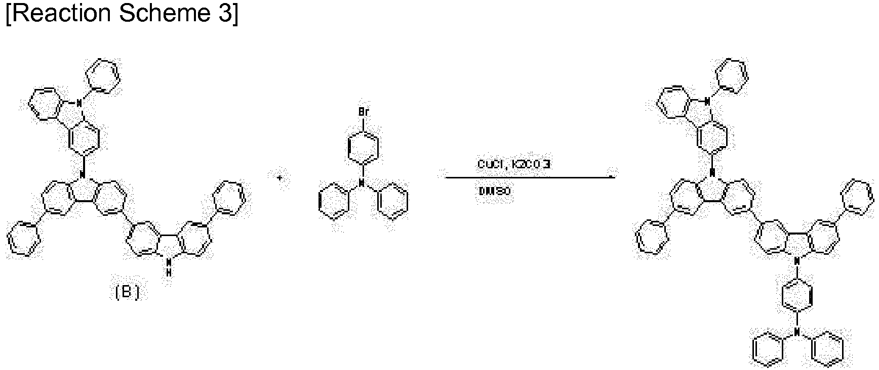
- 2 g (2.76 mmol) of an intermediate product represented by the compound B, 1.3 g (4.1 mmol) of N-(4-bromophenyl)diphenylamine and 0.14 g (1.4 mmol) of copper chloride, 1.14 g (8.3 mmol) of potassium carbonate, 0.25 g (1.4 mmol) of 1,10-phenanthroline, and 80 mL of dimethylsulfoxide were put in a 100 mL round flask and heated at 180 °C for 24 hours under a nitrogen current. Then, an organic solvent therein was removed under reduced pressure distillation, and 2 g of a compound 8 (yield: 75 %) was obtained through column chromatography.
- The compound represented by Chemical Formula 10 was element-analyzed. The result is provided as follows.
- calcd. C72H48N4: C, 89.23; H, 4.99; N, 5.78; found: C, 89.65; H, 5.21; N, 5.55
- An organic photoelectric device was fabricated by using a host of the compound represented by Chemical Formula 11 obtained from Example 1 as a host, and a dopant of Ir(PPy)3. The anode was ITO having a thickness of 1000A, and the cathode was aluminum (Al) having a thickness of 1000A.
- The organic photoelectric device was fabricated by cutting an ITO glass substrate having a sheet resistance of 15 Ω/cm2 to a size of 50mm × 50mm × 0.7mm, ultrasonic wave cleaning the same in acetone, isopropyl alcohol, and pure water for 15 minutes for each, and UV ozone cleaning the same to provide an anode for 30 minutes.
- N,N'-di(1-naphthyl)-N,N'-diphenylbenzidine (NPB) (70 nm) and 4,4',4"-tri(N-carbazolyl)triphenylamine (TCTA) (10 nm) were deposited on the upper surface of the substrate under the conditions of a vacuum degree of 650×10-7 Pa and a deposition speed of 0.1 to 0.3 nm/s to provide a hole transport layer (HTL) having a thickness of 900A.
- Subsequently, a 300Å-thick emission layer was prepared by using the compound synthesized in Example 1 under the same vacuum deposition conditions, and a phosphorescence dopant of Ir(PPy)3 was simultaneously deposited. Herein, a deposition rate of phosphorescent dopant was adjusted so that the phosphorescent dopant is present in an amount of 7 wt% based on 100 wt% of emission layer.
- Bis(8-hydroxy-2-methylquinolato)-aluminumbiphenoxide (BAlq) was deposited on the emission layer under the same vacuum deposition conditions to form a hole blocking layer having a thickness of 50 A.
- Then Alq3 was deposited under the same vacuum deposition conditions to provide an electron transport layer (ETL) having a thickness of 200A.
- LiF and Al were sequentially deposited on the upper surface of the electron transport layer (ETL) to fabricate an organic photoelectric device.
- The organic photoelectric device had a structure of ITO/ NPB (70 nm)/TCTA (10 nm)/ EML (compound of Example 1 (93 wt%) + Ir(PPy)3 (7 wt%), 30 nm)/ Balq (5 nm)/ Alq3 (20 nm)/ LiF (1 nm) / Al (100 nm).
- An organic photoelectric device was fabricated in accordance with the same procedure as in Example 4, except that the compound synthezied in Example 2 was used as a host of the emission layer.
- An organic photoelectric device was fabricated in accordance with the same procedure as in Example 4, except that the compound synthezied in Example 3 was used as a host of the emission layer.
- An organic photoelectric device was fabricated in accordance with the same procedure as in Example 4, except that 4,4-N,N-dicarbazolebiphenyl (CBP) was used as a host of the emission layer instead of the compound synthezied in Example 1.
- Each of the obtained organic photoelectric devices according to Examples 4 to 6 and Comparative Example 1 was measured for luminance change, current density change depending upon voltage, and luminous efficiency. The specific measurement methods were as follows and the results are shown in the following Table 1.
- The obtained organic photoelectric device was measured for current value flowing in the unit device while increasing the voltage from 0V to 10V using a current-voltage meter (Keithley 2400), and the measured current value was divided by area to provide the result.
- The obtained organic photoelectric device was measured for luminance using a luminance meter (Minolta Cs-1000A) while increasing the voltage from 0V to 10V.
- The current efficiency (cd/A) and electric power efficiency (lm/W) at the same luminance (1000 cd/m2) were calculated by using luminance and current density from (1) and (2), and voltage
- The results are shown in the following Tables 2 and 3.
-
[Table 1] Host material in an emission layer 1000 cd/m2 Driving voltage Luminous efficiency Electric power efficiency Example 4 Compound of Example 1 6.86 46.43 22.56 Example 5 Compound of Example 2 7.67 48.33 23.47 Example 6 Compound of Example 3 6.20 50.76 26.45 Comparative Example 1 CBP 7.70 42.70 19.20 - Referring to Table 1, Examples 4 to 6 showed more excellent driving voltage and efficiency compared to the reference material, CBP. These results showed that the compounds prepared in Examples 1 to 3 were applied as a material for an organic photoelectric device.
- The present invention is not limited to the embodiments illustrated with the drawings and table, but can be fabricated into various modifications and equivalent arrangements included within the spirit and scope of the appended claims by a person who is ordinarily skilled in this field. Therefore, the aforementioned embodiments should be understood to be exemplary but not limiting the present invention in any way.
Claims (20)
- The compound for an organic photoelectric device represented by the following Chemical Formula 1:
 Ar1 and Ar2 are the same or different and are each independently selected from the group consisting of a substituted or unsubstituted C6 to C30 aryl group and a substituted or unsubstituted C2 to C30 heteroaryl group,Ar3 and Ar4 are the same or different and are each independently selected from the group consisting of hydrogen, a substituted or unsubstituted C6 to C30 aryl group and a substituted or unsubstituted C2 to C30 heteroaryl group, andR1 to R4 are the same or different and are each independently selected from the group consisting of hydrogen, a substituted or unsubstituted C1 to C30 alkyl group, a substituted or unsubstituted C6 to C30 aryl group, and a substituted or unsubstituted C2 to C30 heteroaryl group.
 - The compound for an organic photoelectric device of claim 1, wherein the compound for an organic photoelectric device is represented by the following Chemical Formula 3:
 Ar1 and Ar2 are the same or different and are each independently selected from the group consisting of a substituted or unsubstituted C6 to C30 aryl group and a substituted or unsubstituted C2 to C30 heteroaryl group,Ar3 and Ar4 are the same or different and are each independently selected from the group consisting of hydrogen, a substituted or unsubstituted C6 to C30 aryl group and a substituted or unsubstituted C2 to C30 heteroaryl group, andR1 to R4 are the same or different and are each independently selected from the group consisting of hydrogen, a substituted or unsubstituted C1 to C30 alkyl group, a substituted or unsubstituted C6 to C30 aryl group, and a substituted or unsubstituted C2 to C30 heteroaryl group.
 - The compound for an organic photoelectric device of claim 2, wherein the compound for an organic photoelectric device is represented by the following Chemical Formula 5:
 Ar2 and Ar5 are the same or different and are each independently selected from the group consisting of a substituted or unsubstituted C6 to C30 aryl group and a substituted or unsubstituted C2 to C30 heteroaryl group,Ar3, Ar4 and Ar6 are the same or different and are each independently selected from the group consisting of hydrogen, a substituted or unsubstituted C6 to C30 aryl group and a substituted or unsubstituted C2 to C30 heteroaryl group, andR1 to R6 are the same or different and are each independently selected from the group consisting of hydrogen, a substituted or unsubstituted C1 to C30 alkyl group, a substituted or unsubstituted C6 to C30 aryl group, and a substituted or unsubstituted C2 to C30 heteroaryl group.
 - The compound for an organic photoelectric device of claim 3, wherein Ar5 is a C6 to C12 aryl group, and
Ar2 is a C10 to C20 fused polycyclic group. - The compound for an organic photoelectric device of claim 3, wherein Ar5 is a C6 to C12 aryl group,
Ar2 is selected from the group consisting of a C6 to C30 substituted or unsubstituted an arylamine group, C6 to C30 substituted or unsubstituted aminoaryl group, a substituted or unsubstituted carbazole group, a substituted or unsubstituted pyridine group, a substituted or unsubstituted pyrimidine group, and a substituted or unsubstituted triazine group. - The compound for an organic photoelectric device of claim 1, wherein the compound for an organic photoelectric device is represented by the following Chemical Formula 2:
 Ar1 and Ar2 are the same or different and are each independently selected from the group consisting of a substituted or unsubstituted C6 to C30 aryl group and a substituted or unsubstituted C2 to C30 heteroaryl group,Ar3 and Ar4 are the same or different and are each independently selected from the group consisting of hydrogen, a substituted or unsubstituted C6 to C30 aryl group and a substituted or unsubstituted C2 to C30 heteroaryl group, andR1 to R4 are the same or different and are each independently selected from the group consisting of hydrogen, a substituted or unsubstituted C1 to C30 alkyl group, a substituted or unsubstituted C6 to C30 aryl group, and a substituted or unsubstituted C2 to C30 heteroaryl group.
 - The compound for an organic photoelectric device of claim 6, wherein the compound for an organic photoelectric device is represented by the following Chemical Formula 4:
 Ar2 and Ar5 are the same or different and are each independently selected from the group consisting of a substituted or unsubstituted C6 to C30 aryl group and a substituted or unsubstituted C2 to C30 heteroaryl group,Ar3, Ar4 and Ar6 are the same or different and are each independently selected from the group consisting of hydrogen, a substituted or unsubstituted C6 to C30 aryl group and a substituted or unsubstituted C2 to C30 heteroaryl group,R1 to R6 are the same or different and are each independently selected from the group consisting of hydrogen, a substituted or unsubstituted C1 to C30 alkyl group, a substituted or unsubstituted C6 to C30 aryl group, and a substituted or unsubstituted C2 to C30 heteroaryl group.
 - The compound for an organic photoelectric device of claim 7, wherein Ar5 is a C6 to C12 aryl group, and
Ar2 is a C10 to C20 fused polycyclic group. - The compound for an organic photoelectric device of claim 7, wherein Ar5 is a C6 to C12 aryl group,
Ar2 is selected from the group consisting of a C6 to C30 substituted or unsubstituted an arylamine group, C6 to C30 substituted or unsubstituted aminoaryl group, a substituted or unsubstituted carbazole group, a substituted or unsubstituted pyridine group, a substituted or unsubstituted pyrimidine group, and a substituted or unsubstituted triazine group. - The compound for an organic photoelectric device of claim 1, wherein the compound for an organic photoelectric device is selected from the group consisting of compounds represented by the following Chemical Formulae 6 to 37:


- The compound for an organic photoelectric device of claim 1, wherein the the compound for an organic photoelectric device is selected from the group consisting of compounds represented by the following Chemical Formulae 38 to 72.


- The compound for an organic photoelectric device of claim 1, wherein the compound for an organic photoelectric device is selected from the group consisting of compounds represented by the following Chemical Formulae 73 to 83.


- An organic photoelectric device comprising
an anode, a cathode, and at least one organic thin layer disposed between the anode and cathode,
wherein at least one the organic thin layer comprises the compound according to one of claims 1 to 12. - The organic photoelectric device of claim 13, wherein the organic thin layer is selected from the group consisting of an emission layer, a hole transport layer (HTL), a hole injection layer (HIL), an electron transport layer (ETL), an electron injection layer (EIL), a hole blocking layer, and a combination thereof.
- The organic photoelectric device of claim 13, wherein the compound for an organic photoelectric device is included in an electron transport layer (ETL) or an electron injection layer (EIL).
- The organic photoelectric device of claim 13, wherein the compound for an organic photoelectric device is included in an emission layer.
- The organic photoelectric device of claim 13, wherein the compound for an organic photoelectric device is used as a phosphorescent or fluorescent host material in an emission layer.
- The organic photoelectric device of claim 13, wherein the compound for an organic photoelectric device the compound is used as a fluorescent blue dopant material in an emission layer.
- The organic photoelectric device of claim 13, wherein the organic photoelectric device is selected from the group consisting of an organic light emitting diode, an organic solar cell, an organic transistor, an organic photo-conductor drum, and an organic memory device.
- A display device comprising an organic photoelectric device according to claim 13.
Priority Applications (1)
| Application Number | Priority Date | Filing Date | Title |
|---|---|---|---|
| EP18190817.9A EP3460024B1 (en) | 2009-11-03 | 2010-10-29 | Compound for an organic photoelectric device, and organic photoelectric device comprising same |
Applications Claiming Priority (2)
| Application Number | Priority Date | Filing Date | Title |
|---|---|---|---|
| KR1020090105576A KR101506999B1 (en) | 2009-11-03 | 2009-11-03 | Compound for organic photoelectric device and organic photoelectric device including the same |
| PCT/KR2010/007550 WO2011055934A2 (en) | 2009-11-03 | 2010-10-29 | Compound for an organic photoelectric device, and organic photoelectric device comprising same |
Related Child Applications (2)
| Application Number | Title | Priority Date | Filing Date |
|---|---|---|---|
| EP18190817.9A Division EP3460024B1 (en) | 2009-11-03 | 2010-10-29 | Compound for an organic photoelectric device, and organic photoelectric device comprising same |
| EP18190817.9A Division-Into EP3460024B1 (en) | 2009-11-03 | 2010-10-29 | Compound for an organic photoelectric device, and organic photoelectric device comprising same |
Publications (3)
| Publication Number | Publication Date |
|---|---|
| EP2497811A2 true EP2497811A2 (en) | 2012-09-12 |
| EP2497811A4 EP2497811A4 (en) | 2013-09-11 |
| EP2497811B1 EP2497811B1 (en) | 2018-12-19 |
Family
ID=43970508
Family Applications (2)
| Application Number | Title | Priority Date | Filing Date |
|---|---|---|---|
| EP18190817.9A Active EP3460024B1 (en) | 2009-11-03 | 2010-10-29 | Compound for an organic photoelectric device, and organic photoelectric device comprising same |
| EP10828469.6A Active EP2497811B1 (en) | 2009-11-03 | 2010-10-29 | Compound for an organic photoelectric device, and organic photoelectric device comprising same |
Family Applications Before (1)
| Application Number | Title | Priority Date | Filing Date |
|---|---|---|---|
| EP18190817.9A Active EP3460024B1 (en) | 2009-11-03 | 2010-10-29 | Compound for an organic photoelectric device, and organic photoelectric device comprising same |
Country Status (6)
| Country | Link |
|---|---|
| US (2) | US20120211736A1 (en) |
| EP (2) | EP3460024B1 (en) |
| JP (1) | JP2013510141A (en) |
| KR (1) | KR101506999B1 (en) |
| CN (2) | CN105670610B (en) |
| WO (1) | WO2011055934A2 (en) |
Cited By (11)
| Publication number | Priority date | Publication date | Assignee | Title |
|---|---|---|---|---|
| EP2415769A1 (en) | 2010-04-20 | 2012-02-08 | Idemitsu Kosan Co., Ltd. | Bis-carbazole derivative, material for organic electroluminescent element and organic electroluminescent element using same |
| EP2471771A1 (en) * | 2009-08-28 | 2012-07-04 | Hodogaya Chemical Co., Ltd. | Organic electroluminescent element and compound having carbazole ring structure |
| EP2674418A1 (en) * | 2011-02-07 | 2013-12-18 | Idemitsu Kosan Co., Ltd. | Biscarbazole derivative and organic electroluminescent element using same |
| EP2688120A1 (en) * | 2011-03-14 | 2014-01-22 | Toray Industries, Inc. | Light-emitting element material and light-emitting element |
| US9373802B2 (en) | 2011-02-07 | 2016-06-21 | Idemitsu Kosan Co., Ltd. | Biscarbazole derivatives and organic electroluminescence device employing the same |
| US9450193B2 (en) | 2009-11-03 | 2016-09-20 | Samsung Sdi Co., Ltd. | Compound for organic photoelectric device and organic photoelectric device including the same |
| US9478755B2 (en) | 2009-11-03 | 2016-10-25 | Cheil Industries, Inc. | Compound for organic photoelectric device and organic photoelectric device including the same |
| US9496508B2 (en) | 2011-12-07 | 2016-11-15 | Idemitsu Kosan Co., Ltd. | Material for organic electroluminescent element and organic electroluminescent element using same |
| US10069081B2 (en) | 2012-12-07 | 2018-09-04 | Universal Display Corporation | Organic electroluminescent materials and devices |
| US11552256B2 (en) | 2014-07-25 | 2023-01-10 | Semiconductor Energy Laboratory Co., Ltd. | Light-emitting element, light-emitting device, electronic device, lighting device, and organic compound |
| WO2023208899A1 (en) | 2022-04-28 | 2023-11-02 | Merck Patent Gmbh | Materials for organic electroluminescent devices |
Families Citing this family (80)
| Publication number | Priority date | Publication date | Assignee | Title |
|---|---|---|---|---|
| KR101233380B1 (en) * | 2009-10-21 | 2013-02-15 | 제일모직주식회사 | Novel compound for organic photoelectric device and organic photoelectric device including the same |
| KR20110122051A (en) | 2010-05-03 | 2011-11-09 | 제일모직주식회사 | Compound for organic photoelectric device and organic photoelectric device including the same |
| JP6007467B2 (en) * | 2010-07-27 | 2016-10-12 | コニカミノルタ株式会社 | Organic electroluminescence element material, organic electroluminescence element, |
| US9954180B2 (en) | 2010-08-20 | 2018-04-24 | Universal Display Corporation | Bicarbazole compounds for OLEDs |
| JP5623996B2 (en) * | 2010-09-21 | 2014-11-12 | 株式会社半導体エネルギー研究所 | Carbazole derivatives |
| KR101531612B1 (en) | 2010-12-02 | 2015-06-25 | 제일모직 주식회사 | Compound for organic photoelectric device and organic photoelectric device including the same |
| JPWO2012086170A1 (en) | 2010-12-20 | 2014-05-22 | 出光興産株式会社 | Aromatic heterocyclic derivative and organic electroluminescence device using the same |
| KR101478000B1 (en) * | 2010-12-21 | 2015-01-05 | 롬엔드하스전자재료코리아유한회사 | Novel organic electroluminescent compounds and organic electroluminescent device using the same |
| CN103429570A (en) * | 2011-03-24 | 2013-12-04 | 出光兴产株式会社 | Biscarbazole derivative and organic electroluminescent element using same |
| TW201638086A (en) * | 2011-03-25 | 2016-11-01 | 出光興產股份有限公司 | Organic electroluminescence device |
| JP6197265B2 (en) * | 2011-03-28 | 2017-09-20 | 東レ株式会社 | Light emitting device material and light emitting device |
| US9391288B2 (en) | 2011-05-12 | 2016-07-12 | Toray Industries, Inc. | Light emitting device material and light emitting device |
| KR101443756B1 (en) | 2011-05-26 | 2014-09-23 | 제일모직 주식회사 | Compound for organic OPTOELECTRONIC device, ORGANIC LIGHT EMITTING DIODE INCLUDING THE SAME and DISPLAY INCLUDING THE organic LIGHT EMITTING DIODE |
| KR101354638B1 (en) | 2011-06-20 | 2014-01-22 | 제일모직주식회사 | MATERIAL for organic OPTOELECTRONIC device, ORGANIC LIGHT EMITTING DIODE INCLUDING THE SAME and DISPLAY INCLUDING THE organic LIGHT EMITTING DIODE |
| KR20130011955A (en) * | 2011-07-21 | 2013-01-30 | 롬엔드하스전자재료코리아유한회사 | Novel organic electroluminescence compounds and organic electroluminescence device using the same |
| WO2013012298A1 (en) * | 2011-07-21 | 2013-01-24 | Rohm And Haas Electronic Materials Korea Ltd. | 9h-carbazole compounds and electroluminescent devices involving them |
| JP6034005B2 (en) * | 2011-08-03 | 2016-11-30 | 出光興産株式会社 | Biscarbazole derivative and organic electroluminescence device using the same |
| KR101474797B1 (en) | 2011-08-08 | 2014-12-19 | 제일모직 주식회사 | Compound for organic optoelectronic device and organic light emitting diode including the same |
| CN103732591A (en) * | 2011-08-18 | 2014-04-16 | 出光兴产株式会社 | Biscarbazole derivative and organic electroluminescent element using same |
| KR20130020398A (en) * | 2011-08-19 | 2013-02-27 | 제일모직주식회사 | Compound for organic optoelectronic device, organic light emitting diode including the same and display including the organic light emitting diode |
| WO2013035329A1 (en) * | 2011-09-09 | 2013-03-14 | 出光興産株式会社 | Organic electroluminescence element |
| WO2013062075A1 (en) * | 2011-10-26 | 2013-05-02 | 出光興産株式会社 | Organic electroluminescence element, and material for organic electroluminescence element |
| WO2013077362A1 (en) * | 2011-11-22 | 2013-05-30 | 出光興産株式会社 | Aromatic heterocyclic derivative, material for organic electroluminescent element, and organic electroluminescent element |
| KR20130062583A (en) * | 2011-12-05 | 2013-06-13 | 롬엔드하스전자재료코리아유한회사 | Novel organic electroluminescence compounds and organic electroluminescence device using the same |
| US9530969B2 (en) | 2011-12-05 | 2016-12-27 | Idemitsu Kosan Co., Ltd. | Material for organic electroluminescence device and organic electroluminescence device |
| EP2790239B1 (en) * | 2011-12-05 | 2020-02-05 | Idemitsu Kosan Co., Ltd | Material for organic electroluminescent element and organic electroluminescent element |
| KR101497133B1 (en) | 2011-12-23 | 2015-02-27 | 제일모직 주식회사 | Compound for organic OPTOELECTRONIC device, ORGANIC LIGHT EMITTING DIODE INCLUDING THE SAME and DISPLAY INCLUDING THE organic LIGHT EMITTING DIODE |
| JPWO2013105206A1 (en) | 2012-01-10 | 2015-05-11 | 出光興産株式会社 | Material for organic electroluminescence element and element using the same |
| US9627625B2 (en) | 2012-02-15 | 2017-04-18 | Toray Industries, Inc. | Light-emitting device material and light-emitting device |
| KR20150030660A (en) * | 2012-06-14 | 2015-03-20 | 유니버셜 디스플레이 코포레이션 | Biscarbazole derivative host materials and red emitter for oled emissive region |
| US9966541B2 (en) | 2012-06-14 | 2018-05-08 | Idemitsu Kosan Co. Ltd. | Biscarbazole derivative host materials and green emitter for OLED emissive region |
| KR102148539B1 (en) * | 2012-06-18 | 2020-08-26 | 토소가부시키가이샤 | Cyclic azine compound, method for producing same, and organic electroluminescent element containing same |
| WO2014007022A1 (en) * | 2012-07-06 | 2014-01-09 | 東レ株式会社 | Light emitting element material and light emitting element |
| KR102099661B1 (en) * | 2012-07-19 | 2020-04-10 | 닛테츠 케미컬 앤드 머티리얼 가부시키가이샤 | Organic electroluminescent element |
| CN104488105B (en) | 2012-07-25 | 2017-03-22 | 东丽株式会社 | Light emitting element material and light emitting element |
| JP2015216136A (en) * | 2012-08-17 | 2015-12-03 | 出光興産株式会社 | Organic electroluminescent element |
| KR101497138B1 (en) * | 2012-08-21 | 2015-02-27 | 제일모직 주식회사 | Organic optoelectronic device and display including the same |
| US20140131665A1 (en) * | 2012-11-12 | 2014-05-15 | Universal Display Corporation | Organic Electroluminescent Device With Delayed Fluorescence |
| CN103524497B (en) * | 2012-11-20 | 2015-08-05 | Tcl集团股份有限公司 | Bipolarity phosphorescence host compound, preparation method and application and electroluminescent device |
| WO2014087657A1 (en) * | 2012-12-07 | 2014-06-12 | 出光興産株式会社 | Aromatic amine derivative and organic electroluminescent element |
| KR101593182B1 (en) * | 2012-12-12 | 2016-02-19 | 삼성전자 주식회사 | Compound for organic optoelectronic device, organic light emitting diode including the same and display including the organic light emitting diode |
| KR102055684B1 (en) | 2012-12-27 | 2020-01-23 | 삼성디스플레이 주식회사 | Organic light emitting diode comprising the same |
| CN107325050A (en) * | 2012-12-28 | 2017-11-07 | 出光兴产株式会社 | Organic electroluminescent element |
| KR101447961B1 (en) | 2013-02-01 | 2014-10-13 | (주)피엔에이치테크 | Novel compound for organic electroluminescent device and organic electroluminescent device comprising the same |
| KR102104633B1 (en) * | 2013-02-15 | 2020-04-27 | 에스에프씨주식회사 | Novel organic compounds for organic light-emitting diode and organic light-emitting diode including the same |
| JP2014196251A (en) * | 2013-03-29 | 2014-10-16 | 出光興産株式会社 | Hetero-arene derivative, organic electroluminescence element material, and organic electroluminescence element |
| KR101566434B1 (en) * | 2013-07-15 | 2015-11-06 | 삼성디스플레이 주식회사 | Organic light emitting device |
| JP6381874B2 (en) * | 2013-07-18 | 2018-08-29 | 三星ディスプレイ株式會社Samsung Display Co.,Ltd. | Material for organic electroluminescence device and organic electroluminescence device using the same |
| CN105339365B (en) * | 2013-07-23 | 2018-01-26 | 出光兴产株式会社 | Novel compound and organic electroluminescent element using same |
| KR101547065B1 (en) * | 2013-07-29 | 2015-08-25 | 주식회사 엘지화학 | Hetero-cyclic compound and organic light emitting device comprising the same |
| JP6627508B2 (en) * | 2013-08-14 | 2020-01-08 | コニカミノルタ株式会社 | Organic electroluminescent element, lighting device, display device, and fluorescent compound |
| KR101649683B1 (en) * | 2013-09-06 | 2016-08-19 | 제일모직 주식회사 | Composition for organic optoelectric device and organic optoelectric device and display device |
| WO2015072470A1 (en) * | 2013-11-12 | 2015-05-21 | 国立大学法人九州大学 | Light-emitting material, and long-persistent phosphor and organic light-emitting element each produced using same |
| KR101577121B1 (en) * | 2013-12-27 | 2015-12-14 | 주식회사 두산 | Organic compounds and organic electro luminescence device comprising the same |
| KR101846436B1 (en) * | 2014-01-29 | 2018-04-06 | 제일모직 주식회사 | Composition for electron transport buffer layer and organic optoelectric device including the electron transport buffer layer and display device |
| KR102280686B1 (en) | 2014-02-11 | 2021-07-22 | 삼성전자주식회사 | Carbazole-based compound and organic light emitting device including the same |
| KR20150099192A (en) * | 2014-02-21 | 2015-08-31 | 삼성에스디아이 주식회사 | Organic optoelectric device and display device |
| KR20150108330A (en) * | 2014-03-17 | 2015-09-25 | 롬엔드하스전자재료코리아유한회사 | Electron buffering material and organic electroluminescent device comprising the same |
| WO2015142036A1 (en) * | 2014-03-17 | 2015-09-24 | Rohm And Haas Electronic Materials Korea Ltd. | Electron buffering material and organic electroluminescent device comprising the same |
| KR102255197B1 (en) * | 2014-05-02 | 2021-05-25 | 삼성디스플레이 주식회사 | Organic light emitting device |
| KR102253443B1 (en) * | 2014-05-13 | 2021-05-20 | 삼성디스플레이 주식회사 | Organic light-emitting devices |
| US10461260B2 (en) * | 2014-06-03 | 2019-10-29 | Universal Display Corporation | Organic electroluminescent materials and devices |
| KR102300023B1 (en) * | 2014-06-13 | 2021-09-09 | 삼성디스플레이 주식회사 | Organic light-emitting devices and method for manufacturing the same |
| KR102430648B1 (en) * | 2014-09-05 | 2022-08-09 | 롬엔드하스전자재료코리아유한회사 | A Hole Transport Material and an Organic Electroluminescent Device Comprising the Same |
| KR102304720B1 (en) * | 2014-09-19 | 2021-09-27 | 삼성디스플레이 주식회사 | Organic light-emitting device |
| KR101818581B1 (en) * | 2014-10-31 | 2018-01-15 | 삼성에스디아이 주식회사 | Organic optoelectric device and display device |
| KR102285388B1 (en) * | 2014-11-13 | 2021-08-04 | 삼성디스플레이 주식회사 | Organic light emitting device |
| KR102343572B1 (en) * | 2015-03-06 | 2021-12-28 | 삼성디스플레이 주식회사 | Organic light emitting device |
| KR101958833B1 (en) * | 2015-09-21 | 2019-03-15 | 삼성에스디아이 주식회사 | Organic optoelectric device and display device |
| US10651392B2 (en) | 2015-09-30 | 2020-05-12 | Samsung Electronics Co., Ltd. | Organic light-emitting device |
| KR102507371B1 (en) * | 2015-12-03 | 2023-03-08 | 솔루스첨단소재 주식회사 | Organic light-emitting compound and organic electroluminescent device using the same |
| KR101872349B1 (en) * | 2016-04-29 | 2018-06-28 | 제일모직 주식회사 | Composition for organic optoelectric device and organic optoelectric device and display device |
| KR101693744B1 (en) * | 2016-05-11 | 2017-02-06 | 희성소재 (주) | Hetero-cyclic compound and organic light emitting device using the same |
| KR102063663B1 (en) | 2016-06-23 | 2020-01-08 | 삼성에스디아이 주식회사 | Compound for organic optoelectronic device, composition for organic optoelectronic device and organic optoelectronic device and display device |
| JP2018163975A (en) * | 2017-03-24 | 2018-10-18 | 出光興産株式会社 | Composition, material for organic electroluminescent element, composition film, organic electroluminescence element, and electronic device |
| CN108276325A (en) * | 2017-10-25 | 2018-07-13 | 吉林奥来德光电材料股份有限公司 | Electroluminescent organic material and preparation method thereof and organic electroluminescence device |
| JP2019116461A (en) * | 2017-12-27 | 2019-07-18 | 三星電子株式会社Samsung Electronics Co.,Ltd. | Compound, liquid composition for organic electroluminescent element, ink composition for organic electroluminescent element, thin film for organic electroluminescent element, and organic electroluminescent element |
| CN110854293B (en) * | 2018-12-10 | 2021-04-20 | 广州华睿光电材料有限公司 | Nitrogen heterocyclic compound, composition, high polymer and organic electroluminescent device |
| KR102495275B1 (en) * | 2019-10-02 | 2023-02-01 | 삼성에스디아이 주식회사 | Compound for organic optoelectronic device, organic optoelectronic device and display device |
| KR20240010669A (en) * | 2022-07-15 | 2024-01-24 | 삼성에스디아이 주식회사 | Compound for organic optoelectronic device, composition for organic optoelectronic device, organic optoelectronic device and display device |
Citations (10)
| Publication number | Priority date | Publication date | Assignee | Title |
|---|---|---|---|---|
| JPH083547A (en) | 1994-03-31 | 1996-01-09 | Toray Ind Inc | Luminous element |
| US20020045061A1 (en) | 2000-03-27 | 2002-04-18 | Idemitsu Kosan Co., Ltd. | Organic electroluminescence element |
| EP1486550A1 (en) | 2002-03-15 | 2004-12-15 | Idemitsu Kosan Co., Ltd. | Material for organic electroluminescent devices and organic electroluminescent devices made by using the same |
| US20060046172A1 (en) | 2004-08-30 | 2006-03-02 | Violeta Vaitkeviciene | Polymeric charge transport materials having carbazolyl repeating units |
| US20060180806A1 (en) | 2003-01-24 | 2006-08-17 | Takashi Arakane | Organic electroluminescence device |
| WO2007119816A1 (en) | 2006-04-19 | 2007-10-25 | Konica Minolta Holdings, Inc. | Organic electroluminescence element material, organic electroluminescence element, display device and lighting apparatus |
| JP2008135498A (en) | 2006-11-28 | 2008-06-12 | Toray Ind Inc | Light emitting element |
| US20080145699A1 (en) | 2004-12-24 | 2008-06-19 | Pioneer Corporation | Organic Compound, Charge-Transporting Material, and Organic Electroluminescent Element |
| EP1970976A1 (en) | 2006-01-05 | 2008-09-17 | Konica Minolta Holdings, Inc. | Organic electroluminescent device, display and illuminating device |
| WO2009060779A1 (en) | 2007-11-08 | 2009-05-14 | Konica Minolta Holdings, Inc. | Organic electroluminescent device material, organic electroluminescent device, display device and illuminating device |
Family Cites Families (23)
| Publication number | Priority date | Publication date | Assignee | Title |
|---|---|---|---|---|
| JPS62124242A (en) | 1985-11-22 | 1987-06-05 | Mitsubishi Alum Co Ltd | Manufacture of high-strength aluminum alloy member |
| JPH05114329A (en) | 1991-10-21 | 1993-05-07 | Nissha Printing Co Ltd | Transparent touch panel with display design |
| JPH11329737A (en) * | 1998-03-13 | 1999-11-30 | Taiho Ind Co Ltd | Organic multilayer type electroluminescent element and synthesizing method of structure body for organic multilayer type electroluminescent element |
| KR100346984B1 (en) * | 2000-02-08 | 2002-07-31 | 삼성에스디아이 주식회사 | Hole Transporting Compound Having Good Thermal Stability for Organic Electroluminescent Devices and Method for the Same |
| JP4707082B2 (en) | 2002-11-26 | 2011-06-22 | コニカミノルタホールディングス株式会社 | Organic electroluminescence element and display device |
| WO2004072205A2 (en) | 2003-02-12 | 2004-08-26 | Koninklijke Philips Electronics N.V. | Carbazole compounds and use of such compounds in organic electroluminescent devices |
| WO2006025186A1 (en) * | 2004-09-01 | 2006-03-09 | Hirose Engineering Co., Ltd. | Dicarbazyl compound, process for producing the same, dicarbazyl polymer, and luminescent element |
| JP2009524703A (en) | 2005-12-20 | 2009-07-02 | コーニンクレッカ フィリップス エレクトロニクス エヌ ヴィ | High molecular carbazole compounds |
| US7381985B1 (en) * | 2006-12-13 | 2008-06-03 | General Electric Company | Bis-carbazole monomers and polymers |
| WO2008090912A1 (en) * | 2007-01-23 | 2008-07-31 | Konica Minolta Holdings, Inc. | Method for manufacturing organic electroluminescent device, organic electroluminescent device manufactured by the method, display device and illuminating device |
| US7723722B2 (en) | 2007-03-23 | 2010-05-25 | Semiconductor Energy Laboratory Co., Ltd. | Organic compound, anthracene derivative, and light-emitting element, light-emitting device, and electronic device using anthracene derivative |
| JP4915279B2 (en) * | 2007-05-23 | 2012-04-11 | 東レ株式会社 | Light emitting element |
| WO2008156105A1 (en) * | 2007-06-21 | 2008-12-24 | Konica Minolta Holdings, Inc. | Organic electroluminescence element material, organic electroluminescence element, display device and illuminating device |
| JP5691170B2 (en) | 2007-11-08 | 2015-04-01 | コニカミノルタ株式会社 | Method for manufacturing organic electroluminescence element |
| US20090153034A1 (en) | 2007-12-13 | 2009-06-18 | Universal Display Corporation | Carbazole-containing materials in phosphorescent light emittinig diodes |
| JPWO2009084413A1 (en) | 2007-12-28 | 2011-05-19 | コニカミノルタホールディングス株式会社 | ORGANIC ELECTROLUMINESCENT ELEMENT AND METHOD FOR PRODUCING ORGANIC ELECTROLUMINESCENT ELEMENT |
| DE102009023155A1 (en) * | 2009-05-29 | 2010-12-02 | Merck Patent Gmbh | Materials for organic electroluminescent devices |
| KR101431644B1 (en) | 2009-08-10 | 2014-08-21 | 롬엔드하스전자재료코리아유한회사 | Novel organic electroluminescent compounds and organic electroluminescent device using the same |
| KR101506999B1 (en) | 2009-11-03 | 2015-03-31 | 제일모직 주식회사 | Compound for organic photoelectric device and organic photoelectric device including the same |
| KR101867105B1 (en) | 2010-03-31 | 2018-06-12 | 이데미쓰 고산 가부시키가이샤 | Material for organic electroluminescence element, and organic electroluminescence element using same |
| CN102421772B (en) | 2010-04-20 | 2015-11-25 | 出光兴产株式会社 | Bicarbazole derivative, material for organic electroluminescent element, and organic electroluminescent element using same |
| US8227801B2 (en) | 2010-04-26 | 2012-07-24 | Universal Display Corporation | Bicarbzole containing compounds for OLEDs |
| KR101874657B1 (en) | 2011-02-07 | 2018-07-04 | 이데미쓰 고산 가부시키가이샤 | Biscarbazole derivative and organic electroluminescent element using same |
-
2009
- 2009-11-03 KR KR1020090105576A patent/KR101506999B1/en active IP Right Grant
-
2010
- 2010-10-29 JP JP2012537800A patent/JP2013510141A/en active Pending
- 2010-10-29 EP EP18190817.9A patent/EP3460024B1/en active Active
- 2010-10-29 CN CN201610195985.7A patent/CN105670610B/en active Active
- 2010-10-29 WO PCT/KR2010/007550 patent/WO2011055934A2/en active Application Filing
- 2010-10-29 CN CN2010800498604A patent/CN102597158A/en active Pending
- 2010-10-29 EP EP10828469.6A patent/EP2497811B1/en active Active
-
2012
- 2012-05-03 US US13/463,211 patent/US20120211736A1/en not_active Abandoned
-
2014
- 2014-10-20 US US14/518,912 patent/US9450193B2/en active Active
Patent Citations (11)
| Publication number | Priority date | Publication date | Assignee | Title |
|---|---|---|---|---|
| JPH083547A (en) | 1994-03-31 | 1996-01-09 | Toray Ind Inc | Luminous element |
| US20020045061A1 (en) | 2000-03-27 | 2002-04-18 | Idemitsu Kosan Co., Ltd. | Organic electroluminescence element |
| EP1486550A1 (en) | 2002-03-15 | 2004-12-15 | Idemitsu Kosan Co., Ltd. | Material for organic electroluminescent devices and organic electroluminescent devices made by using the same |
| US20060180806A1 (en) | 2003-01-24 | 2006-08-17 | Takashi Arakane | Organic electroluminescence device |
| US20060046172A1 (en) | 2004-08-30 | 2006-03-02 | Violeta Vaitkeviciene | Polymeric charge transport materials having carbazolyl repeating units |
| US20080145699A1 (en) | 2004-12-24 | 2008-06-19 | Pioneer Corporation | Organic Compound, Charge-Transporting Material, and Organic Electroluminescent Element |
| EP1970976A1 (en) | 2006-01-05 | 2008-09-17 | Konica Minolta Holdings, Inc. | Organic electroluminescent device, display and illuminating device |
| WO2007119816A1 (en) | 2006-04-19 | 2007-10-25 | Konica Minolta Holdings, Inc. | Organic electroluminescence element material, organic electroluminescence element, display device and lighting apparatus |
| US20090302745A1 (en) | 2006-04-19 | 2009-12-10 | Konica Minolta Holdings, Inc. | Organic Electroluminescence Element Material, Organic Electroluminescence Element, Display Device and Lighting Apparatus |
| JP2008135498A (en) | 2006-11-28 | 2008-06-12 | Toray Ind Inc | Light emitting element |
| WO2009060779A1 (en) | 2007-11-08 | 2009-05-14 | Konica Minolta Holdings, Inc. | Organic electroluminescent device material, organic electroluminescent device, display device and illuminating device |
Non-Patent Citations (1)
| Title |
|---|
| See also references of WO2011055934A2 |
Cited By (30)
| Publication number | Priority date | Publication date | Assignee | Title |
|---|---|---|---|---|
| EP2471771A1 (en) * | 2009-08-28 | 2012-07-04 | Hodogaya Chemical Co., Ltd. | Organic electroluminescent element and compound having carbazole ring structure |
| EP2471771A4 (en) * | 2009-08-28 | 2013-01-16 | Hodogaya Chemical Co Ltd | Organic electroluminescent element and compound having carbazole ring structure |
| US9732036B2 (en) | 2009-08-28 | 2017-08-15 | Hodogaya Chemical Co., Ltd. | Compound having carbazole ring structure, and organic electroluminescent device |
| US9450193B2 (en) | 2009-11-03 | 2016-09-20 | Samsung Sdi Co., Ltd. | Compound for organic photoelectric device and organic photoelectric device including the same |
| US9478755B2 (en) | 2009-11-03 | 2016-10-25 | Cheil Industries, Inc. | Compound for organic photoelectric device and organic photoelectric device including the same |
| EP2423209A1 (en) | 2010-04-20 | 2012-02-29 | Idemitsu Kosan Co., Ltd. | Bis-carbazole derivative, material for organic electroluminescent element and organic electroluminescent element using same |
| US10193077B2 (en) | 2010-04-20 | 2019-01-29 | Idemitsu Kosan Co., Ltd. | Biscarbazole derivative, material for organic electroluminescence device and organic electroluminescence device using the same |
| EP2415769A1 (en) | 2010-04-20 | 2012-02-08 | Idemitsu Kosan Co., Ltd. | Bis-carbazole derivative, material for organic electroluminescent element and organic electroluminescent element using same |
| US8865323B2 (en) | 2010-04-20 | 2014-10-21 | Idemitsu Kosan Co., Ltd. | Biscarbazole derivative, material for organic electroluminescence device and organic electroluminescence device using the same |
| US8877352B2 (en) | 2010-04-20 | 2014-11-04 | Idemitsu Kosan Co., Ltd. | Biscarbazole derivative, material for organic electroluminescence device and organic electroluminescence device using the same |
| US8940414B2 (en) | 2010-04-20 | 2015-01-27 | Idemitsu Kosan Co., Ltd. | Biscarbazole derivative, material for organic electroluminescence device and organic electroluminescence device using the same |
| EP2423209B1 (en) * | 2010-04-20 | 2015-08-05 | Idemitsu Kosan Co., Ltd. | Bis-carbazole derivative, material for organic electroluminescent element and organic electroluminescent element using same |
| US10147888B2 (en) | 2011-02-07 | 2018-12-04 | Idemitsu Kosan Co., Ltd. | Biscarbazole derivative and organic electroluminescent element using same |
| US11271171B2 (en) | 2011-02-07 | 2022-03-08 | Idemitsu Kosan Co., Ltd. | Biscarbazole derivative and organic electroluminescent element using same |
| US9373802B2 (en) | 2011-02-07 | 2016-06-21 | Idemitsu Kosan Co., Ltd. | Biscarbazole derivatives and organic electroluminescence device employing the same |
| US10230057B2 (en) | 2011-02-07 | 2019-03-12 | Idemitsu Kosan Co., Ltd. | Biscarbazole derivatives and organic electroluminescence device employing the same |
| EP2674418A1 (en) * | 2011-02-07 | 2013-12-18 | Idemitsu Kosan Co., Ltd. | Biscarbazole derivative and organic electroluminescent element using same |
| EP2674418A4 (en) * | 2011-02-07 | 2014-07-30 | Idemitsu Kosan Co | Biscarbazole derivative and organic electroluminescent element using same |
| US9818958B2 (en) | 2011-02-07 | 2017-11-14 | Idemitsu Kosan Co., Ltd. | Biscarbazole derivatives and organic electroluminescence device employing the same |
| US10147889B2 (en) | 2011-02-07 | 2018-12-04 | Idemitsu Kosan Co., Ltd. | Biscarbazole derivative and organic electroluminescent element using same |
| EP2688120A1 (en) * | 2011-03-14 | 2014-01-22 | Toray Industries, Inc. | Light-emitting element material and light-emitting element |
| US9537107B2 (en) | 2011-03-14 | 2017-01-03 | Toray Industries, Inc. | Light emitting device material and light emitting device |
| EP2688120A4 (en) * | 2011-03-14 | 2014-10-01 | Toray Industries | Light-emitting element material and light-emitting element |
| US9496508B2 (en) | 2011-12-07 | 2016-11-15 | Idemitsu Kosan Co., Ltd. | Material for organic electroluminescent element and organic electroluminescent element using same |
| US10069081B2 (en) | 2012-12-07 | 2018-09-04 | Universal Display Corporation | Organic electroluminescent materials and devices |
| US10910564B2 (en) | 2012-12-07 | 2021-02-02 | Universal Display Corporation | Organic electroluminescent materials and devices |
| US11716902B2 (en) | 2012-12-07 | 2023-08-01 | Universal Display Corporation | Organic electroluminescent materials and devices |
| US11552256B2 (en) | 2014-07-25 | 2023-01-10 | Semiconductor Energy Laboratory Co., Ltd. | Light-emitting element, light-emitting device, electronic device, lighting device, and organic compound |
| US11800799B2 (en) | 2014-07-25 | 2023-10-24 | Semiconductor Energy Laboratory Co., Ltd. | Light-emitting element, light-emitting device, electronic device, lighting device, and organic compound |
| WO2023208899A1 (en) | 2022-04-28 | 2023-11-02 | Merck Patent Gmbh | Materials for organic electroluminescent devices |
Also Published As
| Publication number | Publication date |
|---|---|
| WO2011055934A9 (en) | 2012-10-26 |
| JP2013510141A (en) | 2013-03-21 |
| CN105670610B (en) | 2019-03-19 |
| WO2011055934A3 (en) | 2011-11-03 |
| US9450193B2 (en) | 2016-09-20 |
| EP2497811A4 (en) | 2013-09-11 |
| KR101506999B1 (en) | 2015-03-31 |
| KR20110048840A (en) | 2011-05-12 |
| US20120211736A1 (en) | 2012-08-23 |
| WO2011055934A2 (en) | 2011-05-12 |
| EP3460024A1 (en) | 2019-03-27 |
| US20150069368A1 (en) | 2015-03-12 |
| EP2497811B1 (en) | 2018-12-19 |
| CN105670610A (en) | 2016-06-15 |
| EP3460024B1 (en) | 2021-04-28 |
| CN102597158A (en) | 2012-07-18 |
Similar Documents
| Publication | Publication Date | Title |
|---|---|---|
| EP3460024B1 (en) | Compound for an organic photoelectric device, and organic photoelectric device comprising same | |
| EP2514798B1 (en) | Compound for organic photoelectric device and organic photoelectric device including same | |
| EP2431445B1 (en) | Compound for organic photoelectric device and organic photoelectric device comprising same | |
| EP2799515B1 (en) | Compound for organic optoelectric device, organic light-emitting diode including same, and display device including organic light-emitting diode | |
| KR101508424B1 (en) | Hetero-cyclic compound and organic electronic device comprising the same | |
| KR101565200B1 (en) | New compound and organic light emitting device using the same | |
| KR101297158B1 (en) | Compound for organic photoelectric device and organic photoelectric device including the same | |
| KR101219492B1 (en) | Compound Containing 5-Membered Heterocycle And Organic Electronic Element Using The Same, Terminal Thereof | |
| EP2663609B1 (en) | Compound for organic optoelectronic device, organic light emitting diode including the same and display including the organic light emitting diode | |
| EP2568030A2 (en) | Compound for organic optoelectronic device, organic light emitting diode including same, and display device including organic light emitting diode | |
| KR101638665B1 (en) | New compound and organic light emitting device using the same | |
| KR20110068330A (en) | Spiro carbazole compound and organic electronic element using the same, terminal thereof | |
| KR20120054154A (en) | Chemical and organic electronic element using the same, terminal thereof | |
| KR20110092262A (en) | Compound containing 5-membered heterocycle and organic electronic element using the same, terminal thereof | |
| KR101181277B1 (en) | Compound Containing Indoloacridine And Organic Electronic Element Using The Same, Terminal Thereof | |
| KR101219485B1 (en) | Chemical comprising dibenzocarbazole and organic electroric element using the same, terminal thererof | |
| KR101181276B1 (en) | Compound Containing Indoloacridine And Organic Electronic Element Using The Same, Terminal Thereof | |
| KR20110058250A (en) | Compound containing 5-membered heterocycle and organic electronic element using the same, terminal thereof | |
| KR101181278B1 (en) | Compound Containing Indoloacridine And Organic Electronic Element Using The Same, Terminal Thereof | |
| KR20100125928A (en) | Compound containing at least two 5-membered heterocycle and organic electronic element using the same, terminal thereof | |
| KR101181270B1 (en) | Compound Containing Indoloacridine And Organic Electronic Element Using The Same, Terminal Thereof | |
| KR20100125006A (en) | Compound containing at least two 5-membered heterocycle and organic electronic element using the same, terminal thereof | |
| KR20110133008A (en) | Compound containing 5-membered heterocycle and organic electronic element using the same, terminal thereof | |
| KR20110133009A (en) | Compound containing 5-membered heterocycle and organic electronic element using the same, terminal thereof | |
| KR101146930B1 (en) | Compound Containing At Least Two 5-Membered Heterocycle And Organic Electronic Element Using The Same, Terminal Thereof |
Legal Events
| Date | Code | Title | Description |
|---|---|---|---|
| PUAI | Public reference made under article 153(3) epc to a published international application that has entered the european phase |
Free format text: ORIGINAL CODE: 0009012 |
|
| 17P | Request for examination filed |
Effective date: 20120419 |
|
| AK | Designated contracting states |
Kind code of ref document: A2 Designated state(s): AL AT BE BG CH CY CZ DE DK EE ES FI FR GB GR HR HU IE IS IT LI LT LU LV MC MK MT NL NO PL PT RO RS SE SI SK SM TR |
|
| DAX | Request for extension of the european patent (deleted) | ||
| TPAC | Observations filed by third parties |
Free format text: ORIGINAL CODE: EPIDOSNTIPA |
|
| A4 | Supplementary search report drawn up and despatched |
Effective date: 20130808 |
|
| RIC1 | Information provided on ipc code assigned before grant |
Ipc: H01L 51/00 20060101ALI20130802BHEP Ipc: C09B 57/00 20060101ALI20130802BHEP Ipc: H05B 33/14 20060101ALI20130802BHEP Ipc: C09K 11/06 20060101AFI20130802BHEP Ipc: H01L 51/50 20060101ALI20130802BHEP |
|
| TPAC | Observations filed by third parties |
Free format text: ORIGINAL CODE: EPIDOSNTIPA |
|
| 17Q | First examination report despatched |
Effective date: 20141028 |
|
| GRAP | Despatch of communication of intention to grant a patent |
Free format text: ORIGINAL CODE: EPIDOSNIGR1 |
|
| STAA | Information on the status of an ep patent application or granted ep patent |
Free format text: STATUS: GRANT OF PATENT IS INTENDED |
|
| RIC1 | Information provided on ipc code assigned before grant |
Ipc: C09B 57/00 20060101ALI20180615BHEP Ipc: C09K 11/06 20060101AFI20180615BHEP Ipc: H01L 51/54 20060101ALI20180615BHEP Ipc: H05B 33/14 20060101ALI20180615BHEP |
|
| INTG | Intention to grant announced |
Effective date: 20180717 |
|
| GRAS | Grant fee paid |
Free format text: ORIGINAL CODE: EPIDOSNIGR3 |
|
| GRAA | (expected) grant |
Free format text: ORIGINAL CODE: 0009210 |
|
| STAA | Information on the status of an ep patent application or granted ep patent |
Free format text: STATUS: THE PATENT HAS BEEN GRANTED |
|
| AK | Designated contracting states |
Kind code of ref document: B1 Designated state(s): AL AT BE BG CH CY CZ DE DK EE ES FI FR GB GR HR HU IE IS IT LI LT LU LV MC MK MT NL NO PL PT RO RS SE SI SK SM TR |
|
| REG | Reference to a national code |
Ref country code: GB Ref legal event code: FG4D |
|
| REG | Reference to a national code |
Ref country code: CH Ref legal event code: EP |
|
| REG | Reference to a national code |
Ref country code: IE Ref legal event code: FG4D |
|
| REG | Reference to a national code |
Ref country code: DE Ref legal event code: R096 Ref document number: 602010055978 Country of ref document: DE |
|
| REG | Reference to a national code |
Ref country code: AT Ref legal event code: REF Ref document number: 1078676 Country of ref document: AT Kind code of ref document: T Effective date: 20190115 |
|
| REG | Reference to a national code |
Ref country code: NL Ref legal event code: MP Effective date: 20181219 |
|
| PG25 | Lapsed in a contracting state [announced via postgrant information from national office to epo] |
Ref country code: LV Free format text: LAPSE BECAUSE OF FAILURE TO SUBMIT A TRANSLATION OF THE DESCRIPTION OR TO PAY THE FEE WITHIN THE PRESCRIBED TIME-LIMIT Effective date: 20181219 Ref country code: NO Free format text: LAPSE BECAUSE OF FAILURE TO SUBMIT A TRANSLATION OF THE DESCRIPTION OR TO PAY THE FEE WITHIN THE PRESCRIBED TIME-LIMIT Effective date: 20190319 Ref country code: FI Free format text: LAPSE BECAUSE OF FAILURE TO SUBMIT A TRANSLATION OF THE DESCRIPTION OR TO PAY THE FEE WITHIN THE PRESCRIBED TIME-LIMIT Effective date: 20181219 Ref country code: LT Free format text: LAPSE BECAUSE OF FAILURE TO SUBMIT A TRANSLATION OF THE DESCRIPTION OR TO PAY THE FEE WITHIN THE PRESCRIBED TIME-LIMIT Effective date: 20181219 Ref country code: BG Free format text: LAPSE BECAUSE OF FAILURE TO SUBMIT A TRANSLATION OF THE DESCRIPTION OR TO PAY THE FEE WITHIN THE PRESCRIBED TIME-LIMIT Effective date: 20190319 Ref country code: HR Free format text: LAPSE BECAUSE OF FAILURE TO SUBMIT A TRANSLATION OF THE DESCRIPTION OR TO PAY THE FEE WITHIN THE PRESCRIBED TIME-LIMIT Effective date: 20181219 |
|
| REG | Reference to a national code |
Ref country code: LT Ref legal event code: MG4D |
|
| REG | Reference to a national code |
Ref country code: AT Ref legal event code: MK05 Ref document number: 1078676 Country of ref document: AT Kind code of ref document: T Effective date: 20181219 |
|
| PG25 | Lapsed in a contracting state [announced via postgrant information from national office to epo] |
Ref country code: RS Free format text: LAPSE BECAUSE OF FAILURE TO SUBMIT A TRANSLATION OF THE DESCRIPTION OR TO PAY THE FEE WITHIN THE PRESCRIBED TIME-LIMIT Effective date: 20181219 Ref country code: SE Free format text: LAPSE BECAUSE OF FAILURE TO SUBMIT A TRANSLATION OF THE DESCRIPTION OR TO PAY THE FEE WITHIN THE PRESCRIBED TIME-LIMIT Effective date: 20181219 Ref country code: GR Free format text: LAPSE BECAUSE OF FAILURE TO SUBMIT A TRANSLATION OF THE DESCRIPTION OR TO PAY THE FEE WITHIN THE PRESCRIBED TIME-LIMIT Effective date: 20190320 Ref country code: AL Free format text: LAPSE BECAUSE OF FAILURE TO SUBMIT A TRANSLATION OF THE DESCRIPTION OR TO PAY THE FEE WITHIN THE PRESCRIBED TIME-LIMIT Effective date: 20181219 |
|
| PG25 | Lapsed in a contracting state [announced via postgrant information from national office to epo] |
Ref country code: NL Free format text: LAPSE BECAUSE OF FAILURE TO SUBMIT A TRANSLATION OF THE DESCRIPTION OR TO PAY THE FEE WITHIN THE PRESCRIBED TIME-LIMIT Effective date: 20181219 |
|
| PG25 | Lapsed in a contracting state [announced via postgrant information from national office to epo] |
Ref country code: ES Free format text: LAPSE BECAUSE OF FAILURE TO SUBMIT A TRANSLATION OF THE DESCRIPTION OR TO PAY THE FEE WITHIN THE PRESCRIBED TIME-LIMIT Effective date: 20181219 Ref country code: PL Free format text: LAPSE BECAUSE OF FAILURE TO SUBMIT A TRANSLATION OF THE DESCRIPTION OR TO PAY THE FEE WITHIN THE PRESCRIBED TIME-LIMIT Effective date: 20181219 Ref country code: IT Free format text: LAPSE BECAUSE OF FAILURE TO SUBMIT A TRANSLATION OF THE DESCRIPTION OR TO PAY THE FEE WITHIN THE PRESCRIBED TIME-LIMIT Effective date: 20181219 Ref country code: CZ Free format text: LAPSE BECAUSE OF FAILURE TO SUBMIT A TRANSLATION OF THE DESCRIPTION OR TO PAY THE FEE WITHIN THE PRESCRIBED TIME-LIMIT Effective date: 20181219 Ref country code: PT Free format text: LAPSE BECAUSE OF FAILURE TO SUBMIT A TRANSLATION OF THE DESCRIPTION OR TO PAY THE FEE WITHIN THE PRESCRIBED TIME-LIMIT Effective date: 20190419 |
|
| PG25 | Lapsed in a contracting state [announced via postgrant information from national office to epo] |
Ref country code: RO Free format text: LAPSE BECAUSE OF FAILURE TO SUBMIT A TRANSLATION OF THE DESCRIPTION OR TO PAY THE FEE WITHIN THE PRESCRIBED TIME-LIMIT Effective date: 20181219 Ref country code: SM Free format text: LAPSE BECAUSE OF FAILURE TO SUBMIT A TRANSLATION OF THE DESCRIPTION OR TO PAY THE FEE WITHIN THE PRESCRIBED TIME-LIMIT Effective date: 20181219 Ref country code: IS Free format text: LAPSE BECAUSE OF FAILURE TO SUBMIT A TRANSLATION OF THE DESCRIPTION OR TO PAY THE FEE WITHIN THE PRESCRIBED TIME-LIMIT Effective date: 20190419 Ref country code: EE Free format text: LAPSE BECAUSE OF FAILURE TO SUBMIT A TRANSLATION OF THE DESCRIPTION OR TO PAY THE FEE WITHIN THE PRESCRIBED TIME-LIMIT Effective date: 20181219 Ref country code: SK Free format text: LAPSE BECAUSE OF FAILURE TO SUBMIT A TRANSLATION OF THE DESCRIPTION OR TO PAY THE FEE WITHIN THE PRESCRIBED TIME-LIMIT Effective date: 20181219 |
|
| REG | Reference to a national code |
Ref country code: DE Ref legal event code: R097 Ref document number: 602010055978 Country of ref document: DE |
|
| PLBE | No opposition filed within time limit |
Free format text: ORIGINAL CODE: 0009261 |
|
| STAA | Information on the status of an ep patent application or granted ep patent |
Free format text: STATUS: NO OPPOSITION FILED WITHIN TIME LIMIT |
|
| PG25 | Lapsed in a contracting state [announced via postgrant information from national office to epo] |
Ref country code: DK Free format text: LAPSE BECAUSE OF FAILURE TO SUBMIT A TRANSLATION OF THE DESCRIPTION OR TO PAY THE FEE WITHIN THE PRESCRIBED TIME-LIMIT Effective date: 20181219 Ref country code: AT Free format text: LAPSE BECAUSE OF FAILURE TO SUBMIT A TRANSLATION OF THE DESCRIPTION OR TO PAY THE FEE WITHIN THE PRESCRIBED TIME-LIMIT Effective date: 20181219 |
|
| 26N | No opposition filed |
Effective date: 20190920 |
|
| PG25 | Lapsed in a contracting state [announced via postgrant information from national office to epo] |
Ref country code: SI Free format text: LAPSE BECAUSE OF FAILURE TO SUBMIT A TRANSLATION OF THE DESCRIPTION OR TO PAY THE FEE WITHIN THE PRESCRIBED TIME-LIMIT Effective date: 20181219 |
|
| PG25 | Lapsed in a contracting state [announced via postgrant information from national office to epo] |
Ref country code: TR Free format text: LAPSE BECAUSE OF FAILURE TO SUBMIT A TRANSLATION OF THE DESCRIPTION OR TO PAY THE FEE WITHIN THE PRESCRIBED TIME-LIMIT Effective date: 20181219 |
|
| PG25 | Lapsed in a contracting state [announced via postgrant information from national office to epo] |
Ref country code: MC Free format text: LAPSE BECAUSE OF FAILURE TO SUBMIT A TRANSLATION OF THE DESCRIPTION OR TO PAY THE FEE WITHIN THE PRESCRIBED TIME-LIMIT Effective date: 20181219 |
|
| REG | Reference to a national code |
Ref country code: CH Ref legal event code: PL |
|
| PG25 | Lapsed in a contracting state [announced via postgrant information from national office to epo] |
Ref country code: LI Free format text: LAPSE BECAUSE OF NON-PAYMENT OF DUE FEES Effective date: 20191031 Ref country code: CH Free format text: LAPSE BECAUSE OF NON-PAYMENT OF DUE FEES Effective date: 20191031 Ref country code: LU Free format text: LAPSE BECAUSE OF NON-PAYMENT OF DUE FEES Effective date: 20191029 |
|
| REG | Reference to a national code |
Ref country code: BE Ref legal event code: MM Effective date: 20191031 |
|
| PG25 | Lapsed in a contracting state [announced via postgrant information from national office to epo] |
Ref country code: BE Free format text: LAPSE BECAUSE OF NON-PAYMENT OF DUE FEES Effective date: 20191031 |
|
| GBPC | Gb: european patent ceased through non-payment of renewal fee |
Effective date: 20191029 |
|
| PG25 | Lapsed in a contracting state [announced via postgrant information from national office to epo] |
Ref country code: FR Free format text: LAPSE BECAUSE OF NON-PAYMENT OF DUE FEES Effective date: 20191031 Ref country code: IE Free format text: LAPSE BECAUSE OF NON-PAYMENT OF DUE FEES Effective date: 20191029 Ref country code: GB Free format text: LAPSE BECAUSE OF NON-PAYMENT OF DUE FEES Effective date: 20191029 |
|
| PG25 | Lapsed in a contracting state [announced via postgrant information from national office to epo] |
Ref country code: CY Free format text: LAPSE BECAUSE OF FAILURE TO SUBMIT A TRANSLATION OF THE DESCRIPTION OR TO PAY THE FEE WITHIN THE PRESCRIBED TIME-LIMIT Effective date: 20181219 |
|
| PG25 | Lapsed in a contracting state [announced via postgrant information from national office to epo] |
Ref country code: MT Free format text: LAPSE BECAUSE OF FAILURE TO SUBMIT A TRANSLATION OF THE DESCRIPTION OR TO PAY THE FEE WITHIN THE PRESCRIBED TIME-LIMIT Effective date: 20181219 Ref country code: HU Free format text: LAPSE BECAUSE OF FAILURE TO SUBMIT A TRANSLATION OF THE DESCRIPTION OR TO PAY THE FEE WITHIN THE PRESCRIBED TIME-LIMIT; INVALID AB INITIO Effective date: 20101029 |
|
| PG25 | Lapsed in a contracting state [announced via postgrant information from national office to epo] |
Ref country code: MK Free format text: LAPSE BECAUSE OF FAILURE TO SUBMIT A TRANSLATION OF THE DESCRIPTION OR TO PAY THE FEE WITHIN THE PRESCRIBED TIME-LIMIT Effective date: 20181219 |
|
| P01 | Opt-out of the competence of the unified patent court (upc) registered |
Effective date: 20230528 |
|
| PGFP | Annual fee paid to national office [announced via postgrant information from national office to epo] |
Ref country code: DE Payment date: 20230929 Year of fee payment: 14 |