EP2495639A1 - Input device and display device equipped with same - Google Patents
Input device and display device equipped with same Download PDFInfo
- Publication number
- EP2495639A1 EP2495639A1 EP10826469A EP10826469A EP2495639A1 EP 2495639 A1 EP2495639 A1 EP 2495639A1 EP 10826469 A EP10826469 A EP 10826469A EP 10826469 A EP10826469 A EP 10826469A EP 2495639 A1 EP2495639 A1 EP 2495639A1
- Authority
- EP
- European Patent Office
- Prior art keywords
- input device
- main surface
- disposed
- coloring
- coloring member
- Prior art date
- Legal status (The legal status is an assumption and is not a legal conclusion. Google has not performed a legal analysis and makes no representation as to the accuracy of the status listed.)
- Granted
Links
Images


Classifications
-
- G—PHYSICS
- G06—COMPUTING; CALCULATING OR COUNTING
- G06F—ELECTRIC DIGITAL DATA PROCESSING
- G06F3/00—Input arrangements for transferring data to be processed into a form capable of being handled by the computer; Output arrangements for transferring data from processing unit to output unit, e.g. interface arrangements
- G06F3/01—Input arrangements or combined input and output arrangements for interaction between user and computer
- G06F3/03—Arrangements for converting the position or the displacement of a member into a coded form
- G06F3/041—Digitisers, e.g. for touch screens or touch pads, characterised by the transducing means
- G06F3/0412—Digitisers structurally integrated in a display
-
- G—PHYSICS
- G02—OPTICS
- G02F—OPTICAL DEVICES OR ARRANGEMENTS FOR THE CONTROL OF LIGHT BY MODIFICATION OF THE OPTICAL PROPERTIES OF THE MEDIA OF THE ELEMENTS INVOLVED THEREIN; NON-LINEAR OPTICS; FREQUENCY-CHANGING OF LIGHT; OPTICAL LOGIC ELEMENTS; OPTICAL ANALOGUE/DIGITAL CONVERTERS
- G02F1/00—Devices or arrangements for the control of the intensity, colour, phase, polarisation or direction of light arriving from an independent light source, e.g. switching, gating or modulating; Non-linear optics
- G02F1/01—Devices or arrangements for the control of the intensity, colour, phase, polarisation or direction of light arriving from an independent light source, e.g. switching, gating or modulating; Non-linear optics for the control of the intensity, phase, polarisation or colour
- G02F1/13—Devices or arrangements for the control of the intensity, colour, phase, polarisation or direction of light arriving from an independent light source, e.g. switching, gating or modulating; Non-linear optics for the control of the intensity, phase, polarisation or colour based on liquid crystals, e.g. single liquid crystal display cells
- G02F1/133—Constructional arrangements; Operation of liquid crystal cells; Circuit arrangements
- G02F1/1333—Constructional arrangements; Manufacturing methods
- G02F1/13338—Input devices, e.g. touch panels
-
- G—PHYSICS
- G06—COMPUTING; CALCULATING OR COUNTING
- G06F—ELECTRIC DIGITAL DATA PROCESSING
- G06F3/00—Input arrangements for transferring data to be processed into a form capable of being handled by the computer; Output arrangements for transferring data from processing unit to output unit, e.g. interface arrangements
- G06F3/01—Input arrangements or combined input and output arrangements for interaction between user and computer
- G06F3/03—Arrangements for converting the position or the displacement of a member into a coded form
- G06F3/041—Digitisers, e.g. for touch screens or touch pads, characterised by the transducing means
- G06F3/044—Digitisers, e.g. for touch screens or touch pads, characterised by the transducing means by capacitive means
- G06F3/0445—Digitisers, e.g. for touch screens or touch pads, characterised by the transducing means by capacitive means using two or more layers of sensing electrodes, e.g. using two layers of electrodes separated by a dielectric layer
-
- G—PHYSICS
- G06—COMPUTING; CALCULATING OR COUNTING
- G06F—ELECTRIC DIGITAL DATA PROCESSING
- G06F3/00—Input arrangements for transferring data to be processed into a form capable of being handled by the computer; Output arrangements for transferring data from processing unit to output unit, e.g. interface arrangements
- G06F3/01—Input arrangements or combined input and output arrangements for interaction between user and computer
- G06F3/03—Arrangements for converting the position or the displacement of a member into a coded form
- G06F3/041—Digitisers, e.g. for touch screens or touch pads, characterised by the transducing means
- G06F3/044—Digitisers, e.g. for touch screens or touch pads, characterised by the transducing means by capacitive means
- G06F3/0446—Digitisers, e.g. for touch screens or touch pads, characterised by the transducing means by capacitive means using a grid-like structure of electrodes in at least two directions, e.g. using row and column electrodes
-
- G—PHYSICS
- G06—COMPUTING; CALCULATING OR COUNTING
- G06F—ELECTRIC DIGITAL DATA PROCESSING
- G06F2203/00—Indexing scheme relating to G06F3/00 - G06F3/048
- G06F2203/041—Indexing scheme relating to G06F3/041 - G06F3/045
- G06F2203/04103—Manufacturing, i.e. details related to manufacturing processes specially suited for touch sensitive devices
-
- G—PHYSICS
- G06—COMPUTING; CALCULATING OR COUNTING
- G06F—ELECTRIC DIGITAL DATA PROCESSING
- G06F2203/00—Indexing scheme relating to G06F3/00 - G06F3/048
- G06F2203/041—Indexing scheme relating to G06F3/041 - G06F3/045
- G06F2203/04111—Cross over in capacitive digitiser, i.e. details of structures for connecting electrodes of the sensing pattern where the connections cross each other, e.g. bridge structures comprising an insulating layer, or vias through substrate
Definitions
- the present invention relates to an input device and a display device equipped with the input device.
- Such an input device includes a substrate and a protective member bonded to the substrate with a bonding member interposed therebetween.
- the input device includes coloring members for plural colors covered with the bonding member between the substrate and the protective member, whereby a display pattern is formed in the outer area.
- the thickness of the bonding member between the substrate and the protective member is made to increase to absorb the level difference between the coloring members in order to solve this problem, there is a problem in that the thickness of the input device increases and the size of the input device increases.
- the invention is made in consideration of the above-mentioned problem and an object thereof is to improve the bonding strength between the substrate and the protective member and to suppress an increase in size.
- an input device includes: a substrate having a first main surface and a second main surface located opposite to the first main surface; a protective member having an opposed surface opposite to the first main surface; a bonding member configured to bond the first main surface and the opposed surface to each other; a first coloring member disposed between the first main surface and the opposed surface, the first coloring member being in contact with the bonding member; and a second coloring member disposed on the second main surface and having a color different from a color of the first coloring member.
- the bonding surface of the bonding member can be made to be flat. Accordingly, it is possible to improve the bonding strength between the substrate and the protective member and to suppress an increase in size of the input device.
- FIG. 1 is a plan view illustrating the input device X1 according to the first embodiment of the invention.
- the input device X1 according to this embodiment is a capacitive touch panel.
- the input device X1 includes an input area E I which can be operated for input by a user and an outer area E O located outside the input area E I .
- the outer area E O includes an external conductive area E G which is an area electrically connected to an FPC (Flexible Printed Circuit) (not shown) or the like.
- FPC Flexible Printed Circuit
- the input device X1 includes a substrate 10, a first detection electrode pattern 11, a second detection electrode pattern 12, an insulating film 20, a first protective member 30, a first bonding member 40, a first coloring member 50, and a second coloring member 60.
- Fig. 2A is a cross-sectional view of the input device X1 taken along the line I-I of Fig. 1 .
- Fig. 2B is a cross-sectional view of the input device X1 taken along the line II-II of Fig. 1 .
- Fig. 3 is a cross-sectional view of the input device X1 taken along the line III-III of Fig. 1 .
- the substrate 10 includes a first main surface 10a and a second main surface 10b located opposite to the first main surface 10a, as shown in Figs. 2A and 2B .
- the shape of the substrate 10 in a plan view is rectangular in this embodiment, but is not limited to this shape.
- examples of the material of the substrate 10 include materials having transparency such as glass or plastics.
- the "transparency" means transparency with respect to visible light.
- the first detection electrode pattern 11 is disposed on the second main surface 10b of the substrate 10 in the input area E I .
- the first detection electrode pattern 11 includes first detection electrodes 111, first connection electrodes 112, and first detection lines 113.
- the first detection electrodes 111 have a function of detecting the position of a finger or the like in the direction of arrow B parallel to the main surface of the input device X1.
- the first detection electrodes 111 are arranged in a matrix at predetermined intervals.
- the shape of the first detection electrodes 111 in a plan view is similar to a diamond shape in this embodiment, but is not limited to the shape.
- the material of the first detection electrodes 111 has to have transparency and electrical conductivity, and examples thereof include ITO (Indium Tin Oxide), IZO (Indium Zinc Oxide), ATO (Antimony Tin Oxide), AZO (Al-Doped Zinc Oxide), tin oxide, zinc oxide, and conductive polymers (such as PEDOT and PSS).
- the first detection electrodes 111 are formed as follows. First, the material such as ITO is applied to the second main surface 10b of the substrate 10 to form a film through the use of a sputtering method, a vapor deposition method, or a chemical vapor deposition (CVD) method. A photosensitive resin is formed in a desired pattern, by applying the photosensitive resin to the surface of the film and exposing and developing the photosensitive resin. Subsequently, the film formed of the material such as ITO is etched with a chemical or the like to pattern the film, whereby the first detection electrodes 111 are formed.
- a sputtering method a vapor deposition method
- CVD chemical vapor deposition
- the first connection electrodes 112 have a function of electrically connecting the neighboring first detection electrodes 111 to each other.
- the first connection electrodes 112 are disposed on the second main surface 10b of the substrate 10 in the input area E I .
- the same materials as the first detection electrodes 111 can be used as the materials of the first connection electrodes 112.
- the method of forming the first connection electrodes 112 is the same as forming the first detection electrodes 111.
- the first detection lines 113 have a function of applying a voltage to the first detection electrodes 111.
- the first detection lines 113 are disposed on the second main surface 10b of the substrate 10 in the outer area E O .
- An end of each first detection line 113 is electrically connected to the first detection electrode 111 located at an end of the input area E I out of the first detection electrodes 111.
- the other end of each first detection line 113 is located in the external conductive area E G .
- Examples of the material of the first detection line 113 include conductive materials such as ITO, tin oxide, aluminum, aluminum alloy, silver foil, and silver alloy.
- the method of forming the first detection line 113 is the same as forming the first detection electrode 111.
- the second detection electrode pattern 12 is disposed on the second main surface 10b of the substrate 10 in the input area E I .
- the second detection electrode pattern 12 includes second detection electrodes 121, second connection electrodes 122, and second detection lines 123.
- the second detection electrodes 121 have a function of detecting the position of a finger or the like in the direction of arrow A parallel to the main surface of the input device X1.
- the second detection electrodes 121 are arranged in a matrix at predetermined intervals.
- the shape of the second detection electrodes 121 in a plan view is similar to a diamond shape in this embodiment, but is not limited to the shape.
- the same materials as in the first detection electrodes 111 can be used as the material of the second detection electrodes 121.
- the method of forming the second detection electrodes 121 is the same as forming the first detection electrodes 111.
- the second connection electrodes 122 have a function of electrically connecting the neighboring second detection electrodes 121 to each other.
- the second connection electrodes 122 are disposed on the surface of the insulating film 20. That is, the second connection electrodes 122 intersect the first connection electrodes 112 with the insulating film 20 interposed therebetween.
- the same materials as in the first detection electrodes 111 can be used as the material of the second connection electrodes 122.
- the method of forming the second connection electrodes 122 is the same as forming the first detection electrodes 111.
- the insulating film 20 has a function of insulating the first connection electrodes 112 and the second connection electrodes 122 from each other.
- the insulating film 20 is disposed on the second main surface 10b of the substrate 10 so as to cover the first connection electrodes 112.
- Examples of the material of the insulating film 20 include resins such as an acryl resin and an epoxy resin.
- the insulating film 20 is formed by applying the material to the second main surface 10b of the substrate 10 and exposing and developing the material.
- the second detection lines 123 have a function of applying a voltage to the second detection electrodes 121.
- the second detection lines 123 are disposed on the second main surface 10b of the substrate 10 in the outer area E O .
- An end of each second detection line 123 is electrically connected to the second detection electrode 121 located at an end of the input area E I out of the second detection electrodes 121.
- the other end of each second detection line 123 is located in the external conductive area E G .
- the same materials as in the first detection lines 113 can be used as the material of the second detection line 123.
- the method of forming the second detection line 123 is the same as forming the first detection electrode 111.
- the first protective member 30 has a function of preventing an external conductor such as a finger from coming in direct contact with the first main surface 10a of the substrate 10.
- the first protective member 30 has an opposed surface 30a opposing the first main surface 10a of the substrate 10.
- a user can input information to the input device X1 by bringing a finger into contact with or close to the surface of the first protective member 30 opposite to the opposed surface 30a.
- examples of the material of the first protective member 30 include PET (Polyethylene Terephthalate), acryl, PC (Polycarbonate), and glass.
- Examples of the first protective member 30 include a polarizing plate or a decorative plate.
- the first bonding member 40 has a function of bonding the opposed surface 10a of the first protective member 30 to the first main surface 10a of the substrate 10.
- Examples of the material of the first bonding member 40 include resins having transparency such as an acryl resin, an epoxy resin, and a silicone resin.
- the first coloring member 50 has a function of decorating the outer area E O of the input device X1.
- the first coloring member 50 is disposed on the opposed surface 30a of the first protective member 30 in the outer area E O .
- the first coloring member 50 is in contact with the first bonding member 40.
- the material of the first coloring member 50 include resins such as polyvinyl chloride resins, a polyamide resins, polyester resins, acryl resins, and urethane resins which contain a predetermined color of pigment or dye as a colorant.
- the first coloring member 50 is formed, for example, by screen-printing the material on the opposed surface 30a of the first protective member 30.
- the first coloring member 50 is disposed to cover the first detection lines 113 and the second detection lines 123 in a plan view as in this embodiment.
- the first detection lines 113 and the second detection lines 123 are not visible to the user well.
- the first coloring member 50 in this embodiment is disposed to cover all the first detection lines 113 and all the second detection lines 123, but the first coloring member may be disposed to cover a part of the first detection lines 113 or a part of the second detection lines 123.
- the second coloring member 60 along with the first coloring member 50 has a function of decorating the outer area E O of the input device X1.
- the second coloring member 60 is disposed on the second main surface 10b of the substrate 10.
- the same materials as in the first coloring member 50 can be used as the material of the second coloring member 60.
- the second coloring member 60 has a color different from a color of the first coloring member 50.
- the "different color” means that they are different from each other in at least one of hue, lightness, and chroma in the Munsell color system.
- the first coloring member 50 and the second coloring member 60 are preferably disposed so as not to overlap with each other in a plan view. Accordingly, it is possible to decorate the outer area E O of the input device X1 with two or more colors into a good design.
- the second coloring member 60 is formed by applying the material to the second main surface 10b and exposing and developing the material, unlike the first coloring member 50.
- the first coloring member and the second coloring member are formed between the substrate and the first protective member as in the known input device, the first coloring member is first formed on the opposed surface of the first protective member and then the second coloring member is formed on the opposed surface of the first protective member.
- the first coloring member and the second coloring member are formed by applying the materials of the coloring members to predetermined sites on the opposed surface of the first protective member and exposing and developing the materials.
- the material of the second coloring member is applied to a predetermined site on the opposed surface of the first protective member, a part of the material of the second coloring member runs over the first coloring member due to the surface tension. Accordingly, the second coloring member after curing is thicker than the first coloring member.
- a level difference occurs between the first coloring member and the second coloring member due to the difference in thickness. Since a level difference is present between the first coloring member and the second coloring member, there is a possibility that unevenness may be formed on the bonding surface of the first bonding member to be bonded to the first main surface of the substrate. Accordingly, the flatness of the bonding surface of the first bonding member in the known input device is lowered.
- the first coloring member 50 is disposed on the opposed surface 30a of the first protective member 30 in the outer area E O and the second coloring member 60 is disposed on the second main surface 10b of the substrate 10 in the outer area E O . That is, the second coloring member 60 is not disposed on the opposed surface 30a of the first protective member 30 in the outer area E O but only the first coloring member 50 is disposed thereon. Accordingly, it is possible to suppress the formation of unevenness on the bonding surface of the first bonding member 40, compared with the case where both the first coloring member and the second coloring member are disposed on the opposed surface of the first protective member in the outer area E O as in the known input device.
- the input device X1 it is possible to flatten the bonding surface of the first bonding member 40, compared with the known input device. As a result, it is possible to suppress an increase in size of the input device X1 and to improve the bonding strength between the substrate 10 and the first protective member 30.
- the capacitance between the finger and the detection electrodes 111 and 121 varies.
- a driver (not shown) disposed in the input device X1 always detects the variation in capacitance between the finger and the detection electrodes 111 and 121.
- the driver detects the position from which the variation in capacitance is detected as an input position. In this way, the input device X1 can detect the input position.
- Any of a mutual capacitance method and a self capacitance method can be employed as the input position detecting method in the input device X1.
- the mutual capacitance method is employed, a plurality of input positions can be simultaneously detected, which is preferable in comparison with the case where the self capacitance method is employed.
- Fig. 4 is a diagram showing a first modification of the input device X1 shown in Fig. 1 , corresponding to the cross-section taken along the line III-III of Fig. 1 .
- the differences between the input device X1 shown in Fig. 4 and the input device X1 shown in Fig. 1 are as follows.
- the first coloring member 50 in the input device X1 shown in Fig. 1 is disposed on the opposed surface 30a of the first protective member 30, but the first coloring member 50 in the input device X1 shown in Fig. 4 is disposed on the first main surface 10a of the substrate 10.
- the first coloring member 50 is disposed on the first main surface 10a of the substrate 10, the stress applied to the first coloring member 50 by the press with a finger or the like is reduced, compared with the case where the first coloring member is disposed on the opposed surface 30a of the first protective member 30. Accordingly, it is possible to suppress the deformation of the first coloring member 50 and to keep the state of the design good.
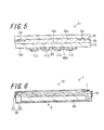
- Fig. 5 is a diagram showing a second modification of the input device X1 shown in Fig. 1 , corresponding to the cross-section taken along the line III-III of Fig. 1 .
- the differences between the input device X1 shown in Fig. 5 and the input device X1 shown in Fig. 1 are as follows.
- the first coloring member 50 in the input device X1 shown in Fig. 1 covers the first detection lines 113 and the second detection lines 123 in a plan view, but the second coloring member 60 in the input device X1 shown in Fig. 5 covers the first detection lines 113 and the second detection lines 123 in a plan view.
- the first detection lines 113 and the second detection lines 123 are disposed on the top surface 60a of the second coloring member 60 disposed on the second main surface 10b of the substrate 10. Accordingly, since the reflected light from the first detection lines 113 and the second detection lines 123 can be satisfactorily absorbed by the second coloring member 60, it is possible to further improve the visibility.
- FIG. 6 is a cross-sectional view of the display device according to this embodiment of the invention.
- the display device Y includes an input device X1 and a liquid crystal display device Z.
- the liquid crystal display device Z includes a liquid crystal display panel 70, a light source device 80, and a case 90.
- Fig. 7 is a perspective view illustrating the liquid crystal display panel 70.
- the liquid crystal display panel 70 includes an upper substrate 71, a lower substrate 72, and a sealing member 73.
- a display area P including a plurality of pixels displaying an image is formed by interposing a liquid crystal layer (not shown) between the upper substrate 71 and the lower substrate 72 and sealing the liquid crystal layer with the sealing member 73.
- the liquid source device 80 serves to emit light to the liquid crystal display panel 70 and is disposed between the liquid crystal display panel 70 and a lower case 92.
- the case 90 is a member receiving the liquid crystal display panel 70 and the light source device 80 and includes an upper case 91 and a lower case 92.
- Examples of the material of the case 90 includes resins such as polycarbonate resins and metals such as stainless steel (SUS) or aluminum.
- the input device X1 and the liquid crystal display device Z are bonded to each other with a double-sided tape T at the edge of the input device X1 and the liquid crystal display device Z.
- the fixing member used to fix the input device X1 and the liquid crystal display device Z is not limited to the double-sided tape T, but an adhesive member such as a thermosetting resin or an ultraviolet-curable resin or a fixing structure physically fixing the input device X1 and the liquid crystal display device Z to each other can be used.
- the behavior of the liquid crystal layer is controlled on a pixel to pixel basis by the use of a liquid crystal driving circuit disposed outside and light from the light source device 80 is transmitted through the liquid crystal display panel 70, whereby an image can be displayed in the display area P.
- the display device Z includes the input device X1 as described above. Accordingly, in the display device Y, it is possible to improve the bonding strength between the substrate 10 and the first protective member 30 and to suppress an increase in size.
- FIG. 8A is a diagram illustrating the input device X2 according to the second embodiment of the invention, corresponding to the cross-sectional view taken along the line I-I of Fig. 1 .
- Fig. 8B is a diagram illustrating the input device X2 according to the second embodiment of the invention, corresponding to the cross-sectional view taken along the line II-II of Fig. 1 .
- Fig. 9 is a diagram illustrating the input device X2 according to the second embodiment of the invention, corresponding to the cross-sectional view taken along the line III-III of Fig. 1 .
- Components having the same functions as in the input device X1 are denoted by the same reference signs and the same description as in the input device X1 will not be repeated.
- the input device X2 is different from the input device X1, in that the input device X2 further includes a second protective member 30A and a second bonding member 40A.
- the input device X2 is also different from the input device X1, in that the second coloring member 60 is disposed in the second protective member 30A.
- the second protective member 30A has a function of suppressing a direct contact of a conductor such as a finger with the first detection electrodes 111 and the second detection electrodes 121 from the outside.
- the second protective member 30A includes an opposed surface 30Aa facing the second main surface 10b of the substrate 10.
- the second bonding member 40A has a function of bonding the second main surface 10b of the substrate 10 and the opposed surface 30Aa of the second protective member 30A to each other.
- the second coloring member 60 is disposed on the opposed surface 30Aa of the second protective member 30A and is covered with the second bonding member 40A.
- the first coloring member 50 is disposed on the opposed surface 30a of the first protective member 30 in the outer area E O and the second coloring member 60 is disposed on the opposed surface 30Aa of the second protective member 30A in the outer area E O . Accordingly, it is possible to flatten the bonding surface of the first bonding member 40, to suppress an increase in size of the input device X2, and to enhance the bonding strength between the substrate 10 and the first protective member 30, which are the same advantages as in the first embodiment.
- the second coloring member 60 is disposed on the opposed surface 30Aa of the second protective member 30A in the outer area E O .
- the resin constituting the second coloring member 60 generally has a dielectric constant lower than that of glass or plastics which is the material of the substrate 10.
- the dielectric constant of glass is equal to or more than about 7.0 but the dielectric constant of the resin constituting the second coloring member 60 is equal to or more than about 3.5. Accordingly, by disposing the second coloring member 60 having a low dielectric constant on the opposed surface 30Aa of the second protective member 30A in the outer area E O , it is possible to reduce floating charge generated between the first detection lines 113 and between the second detection lines 123.
- FIG. 10 is a diagram illustrating the input device X3 according to the third embodiment of the invention, corresponding to the cross-sectional view taken along the line III-III of Fig. 1 .
- Components having the same functions as in the input device X1 are denoted by the same reference signs and the same description as in the input device X1 will not be repeated.
- the input device X3 is different from the input device X1, in that concave holes 51 opened on the opposed surface 50a facing the first bonding member 40 are formed in the first coloring member 50 of the input device X3.
- the shape of the holes 51 and the number of the holes 51 are not particularly limited.
- the first coloring member 50 and the first bonding member 40 are bonded to each other in the state where the first bonding member 40 is buried in the holes 51.
- the bonding area between the first coloring member 50 and the first bonding member 40 increases by the inner wall surfaces of the first coloring member 50 facing the holes 51. By this increase in bonding area, it is possible to enhance the bonding strength between the first coloring member 50 and the first bonding member 40.
- the pressing with a finger or the like is repeatedly performed on the input device X3, but it is possible to reduce the possibility of separating the first coloring member 50 and the first bonding member 40 from each other by enhancing the bonding strength between the first coloring member 50 and the first bonding member 40.
- the holes 51 are preferably distributed uniformly on the opposed surface 50a of the first coloring member 50.
- the holes 51 only have to be formed in the first coloring member 50 with such an aperture size, a hole depth, and a distribution density in the opposed surface 50a not to damage the function of decorating the outer area E O , which is the function inherent to the first coloring member 50.
- the aperture size of the holes 51 is preferably in the range of 20 to 30 ⁇ m.
- the depth of the holes 51 is preferably in the range of 0.5 to 2 ⁇ m.
- the holes 51 are concave holes opened on the opposed surface 50a facing the first bonding member 40
- the invention is not limited to this example.
- the holes 51 may be through-holes.
- the decoration (visibility) of the first coloring member 50 may be lowered.
- the bonding area between the first coloring member 50 and the first bonding member 40 is larger in the inner wall surfaces facing the through holes than in the inner wall surfaces facing the concave holes, the bonding strength between the first coloring member 50 and the first bonding member 40 is further enhanced.
- the outer area E O is decorated with two colors of the first coloring member 50 and the second coloring member 60, but the outer area E O may be decorated with three or more colors by providing another coloring member in addition to the first coloring member 50 and the second coloring member 60.
- information can be input to the input device X1 by causing a user to bring his or her finger or the like into contact with or close to the surface of the first protective member 30 opposite to the opposed surface 30a, but the invention is not limited to this configuration.
- information may be input to the input device X1 by causing a user to bring his or her finger or the like into contact with or close to the surface of the second protective member 30A opposite to the opposed surface 30Aa.
- first coloring member 50 and the second coloring member 60 are disposed so as not to overlap with each other in a plan view, but the first coloring member 50 and the second coloring member 60 may be instead disposed so as to overlap with each other in a plan view at the boundary between the first coloring member 50 and the second coloring member 60. Accordingly, it is possible to suppress, for example, leakage of the light from the light source device 80 through the boundary between the first coloring member 50 and the second coloring member 60.
- the first coloring member 50 is disposed between the first main surface 10a and the opposed surface 30a in the outer area E O and the second coloring member 60 is disposed on the second main surface 10b in the outer area E O , but the invention is not limited to this configuration. That is, the first coloring member 50 may be disposed between the first main surface 10a and the opposed surface 30a in the input area E I and the second coloring member 60 may be disposed on the second main surface 10b in the input area E I . That is, a case where it is necessary to decorate the input area E I can be also considered.
- the input device is a capacitive touch panel, but, for example, a resistive touch panel may be employed instead.
- the resistive touch panel includes an upper substrate having a first transparent electrode on one main surface, a lower substrate disposed to face the upper substrate and having a second transparent electrode on a main surface facing the first transparent electrode, and a protective member disposed on the other main surface of the upper substrate.
- the upper substrate corresponds to the substrate 10
- the protective member corresponds to the first protective member 30.
- the same advantages as in the above-mentioned embodiments can be achieved by disposing the first coloring member between the protective member and the upper substrate in the outer area E O and disposing the second coloring member on one main surface of the upper substrate in the outer area E O .
- the display device Y including the input device X1 has been stated, but the display device Y may include the input device X2 instead of the input device X1.
- the display panel of the display device Y is a liquid crystal display panel, but the invention is not limited to this example. That is, the display panel may be a CRT, a plasma display, an organic EL display, an inorganic EL display, an LED display, a fluorescent display tube, a field emission display, a surface-condition electron-emitter display, or an electronic paper.
- the display panel may be a CRT, a plasma display, an organic EL display, an inorganic EL display, an LED display, a fluorescent display tube, a field emission display, a surface-condition electron-emitter display, or an electronic paper.
Abstract
Description
- The present invention relates to an input device and a display device equipped with the input device.
- Recently, input devices having a display pattern disposed in an outer area located outside an input area for the purpose of improvement in design of the input devices have been known (for example, see Patent Literature 1). Such an input device includes a substrate and a protective member bonded to the substrate with a bonding member interposed therebetween. The input device includes coloring members for plural colors covered with the bonding member between the substrate and the protective member, whereby a display pattern is formed in the outer area.
-
- Patent Literature 1: Japanese Unexamined Patent Publication
JP-A 5-114329 (1993 - However, when a plurality of coloring members are disposed between the substrate and the protective member, a level difference occurs between the coloring members. Since a level difference occurs between the coloring members, the flatness of a bonding surface of the bonding member to be bonded to the substrate is damaged. Accordingly, there is a problem in that air is introduced into gaps of the bonding surface to lower bonding strength between the substrate and the protective member.
- Here, when the thickness of the bonding member between the substrate and the protective member is made to increase to absorb the level difference between the coloring members in order to solve this problem, there is a problem in that the thickness of the input device increases and the size of the input device increases.
- The invention is made in consideration of the above-mentioned problem and an object thereof is to improve the bonding strength between the substrate and the protective member and to suppress an increase in size.
- According to an aspect of the invention, an input device includes: a substrate having a first main surface and a second main surface located opposite to the first main surface; a protective member having an opposed surface opposite to the first main surface; a bonding member configured to bond the first main surface and the opposed surface to each other; a first coloring member disposed between the first main surface and the opposed surface, the first coloring member being in contact with the bonding member; and a second coloring member disposed on the second main surface and having a color different from a color of the first coloring member.
- In the input device according to the invention, the bonding surface of the bonding member can be made to be flat. Accordingly, it is possible to improve the bonding strength between the substrate and the protective member and to suppress an increase in size of the input device.
- Other and further objects, features, and advantages of the invention will be more explicit from the following detailed description taken with reference to the drawings, wherein:
-
Fig. 1 is a plan view illustrating an input device X1 according to a first embodiment of the invention; -
Fig. 2A is a cross-sectional view of the input device X1 taken along the line I-I ofFig. 1 ; -
Fig. 2B is a cross-sectional view of the input device X1 taken along the line II-II ofFig. 1 ; -
Fig. 3 is a cross-sectional view of the input device X1 taken along the line III-III ofFig. 1 ; -
Fig. 4 is a diagram showing a first modification of the input device X1 shown inFig. 1 , corresponding to the cross-section taken along the line III-III ofFig. 1 ; -
Fig. 5 is a diagram showing a second modification of the input device X1 shown inFig. 1 , corresponding to the cross-section taken along the line III-III ofFig. 1 ; -
Fig. 6 is a cross-sectional view of a display device according to an embodiment of the invention; -
Fig. 7 is a perspective view illustrating a liquidcrystal display panel 70; -
Fig. 8A is a diagram illustrating an input device X2 according to a second embodiment of the invention, corresponding to the cross-sectional view taken along the line I-I ofFig. 1 ; -
Fig. 8B is a diagram illustrating the input device X2 according to the second embodiment of the invention, corresponding to the cross-sectional view taken along the line II-II ofFig. 1 ; -
Fig. 9 is a diagram illustrating the input device X2 according to the second embodiment of the invention, corresponding to the cross-sectional view taken along the line III-III ofFig. 1 ; and -
Fig. 10 is a diagram illustrating an input device X3 according to a third embodiment of the invention, corresponding to the cross-sectional view taken along the line III-III ofFig. 1 . - Hereinafter, exemplary embodiments of the invention will be described in detail with reference to the accompanying drawings.
- First, an input device X1 according to a first embodiment of the invention will be described.
Fig. 1 is a plan view illustrating the input device X1 according to the first embodiment of the invention. Here, the input device X1 according to this embodiment is a capacitive touch panel. - As shown in
Fig. 1 , the input device X1 includes an input area EI which can be operated for input by a user and an outer area EO located outside the input area EI. The outer area EO includes an external conductive area EG which is an area electrically connected to an FPC (Flexible Printed Circuit) (not shown) or the like. - As shown in
Figs. 1 to 3 , the input device X1 includes asubstrate 10, a first detection electrode pattern 11, a seconddetection electrode pattern 12, aninsulating film 20, a firstprotective member 30, afirst bonding member 40, afirst coloring member 50, and asecond coloring member 60. -
Fig. 2A is a cross-sectional view of the input device X1 taken along the line I-I ofFig. 1 .Fig. 2B is a cross-sectional view of the input device X1 taken along the line II-II ofFig. 1 .Fig. 3 is a cross-sectional view of the input device X1 taken along the line III-III ofFig. 1 . - The
substrate 10 includes a firstmain surface 10a and a secondmain surface 10b located opposite to the firstmain surface 10a, as shown inFigs. 2A and 2B . The shape of thesubstrate 10 in a plan view is rectangular in this embodiment, but is not limited to this shape. Here, examples of the material of thesubstrate 10 include materials having transparency such as glass or plastics. The "transparency" means transparency with respect to visible light. - The first detection electrode pattern 11 is disposed on the second
main surface 10b of thesubstrate 10 in the input area EI. The first detection electrode pattern 11 includesfirst detection electrodes 111,first connection electrodes 112, andfirst detection lines 113. - The
first detection electrodes 111 have a function of detecting the position of a finger or the like in the direction of arrow B parallel to the main surface of the input device X1. Thefirst detection electrodes 111 are arranged in a matrix at predetermined intervals. The shape of thefirst detection electrodes 111 in a plan view is similar to a diamond shape in this embodiment, but is not limited to the shape. The material of thefirst detection electrodes 111 has to have transparency and electrical conductivity, and examples thereof include ITO (Indium Tin Oxide), IZO (Indium Zinc Oxide), ATO (Antimony Tin Oxide), AZO (Al-Doped Zinc Oxide), tin oxide, zinc oxide, and conductive polymers (such as PEDOT and PSS). For example, thefirst detection electrodes 111 are formed as follows. First, the material such as ITO is applied to the secondmain surface 10b of thesubstrate 10 to form a film through the use of a sputtering method, a vapor deposition method, or a chemical vapor deposition (CVD) method. A photosensitive resin is formed in a desired pattern, by applying the photosensitive resin to the surface of the film and exposing and developing the photosensitive resin. Subsequently, the film formed of the material such as ITO is etched with a chemical or the like to pattern the film, whereby thefirst detection electrodes 111 are formed. - The
first connection electrodes 112 have a function of electrically connecting the neighboringfirst detection electrodes 111 to each other. Thefirst connection electrodes 112 are disposed on the secondmain surface 10b of thesubstrate 10 in the input area EI. The same materials as thefirst detection electrodes 111 can be used as the materials of thefirst connection electrodes 112. The method of forming thefirst connection electrodes 112 is the same as forming thefirst detection electrodes 111. - The
first detection lines 113 have a function of applying a voltage to thefirst detection electrodes 111. Thefirst detection lines 113 are disposed on the secondmain surface 10b of thesubstrate 10 in the outer area EO. An end of eachfirst detection line 113 is electrically connected to thefirst detection electrode 111 located at an end of the input area EI out of thefirst detection electrodes 111. The other end of eachfirst detection line 113 is located in the external conductive area EG. Examples of the material of thefirst detection line 113 include conductive materials such as ITO, tin oxide, aluminum, aluminum alloy, silver foil, and silver alloy. The method of forming thefirst detection line 113 is the same as forming thefirst detection electrode 111. - The second
detection electrode pattern 12 is disposed on the secondmain surface 10b of thesubstrate 10 in the input area EI. The seconddetection electrode pattern 12 includessecond detection electrodes 121,second connection electrodes 122, and second detection lines 123. - The
second detection electrodes 121 have a function of detecting the position of a finger or the like in the direction of arrow A parallel to the main surface of the input device X1. Thesecond detection electrodes 121 are arranged in a matrix at predetermined intervals. The shape of thesecond detection electrodes 121 in a plan view is similar to a diamond shape in this embodiment, but is not limited to the shape. The same materials as in thefirst detection electrodes 111 can be used as the material of thesecond detection electrodes 121. The method of forming thesecond detection electrodes 121 is the same as forming thefirst detection electrodes 111. - The
second connection electrodes 122 have a function of electrically connecting the neighboringsecond detection electrodes 121 to each other. Thesecond connection electrodes 122 are disposed on the surface of the insulatingfilm 20. That is, thesecond connection electrodes 122 intersect thefirst connection electrodes 112 with the insulatingfilm 20 interposed therebetween. The same materials as in thefirst detection electrodes 111 can be used as the material of thesecond connection electrodes 122. The method of forming thesecond connection electrodes 122 is the same as forming thefirst detection electrodes 111. - The insulating
film 20 has a function of insulating thefirst connection electrodes 112 and thesecond connection electrodes 122 from each other. The insulatingfilm 20 is disposed on the secondmain surface 10b of thesubstrate 10 so as to cover thefirst connection electrodes 112. Examples of the material of the insulatingfilm 20 include resins such as an acryl resin and an epoxy resin. The insulatingfilm 20 is formed by applying the material to the secondmain surface 10b of thesubstrate 10 and exposing and developing the material. - The
second detection lines 123 have a function of applying a voltage to thesecond detection electrodes 121. Thesecond detection lines 123 are disposed on the secondmain surface 10b of thesubstrate 10 in the outer area EO. An end of eachsecond detection line 123 is electrically connected to thesecond detection electrode 121 located at an end of the input area EI out of thesecond detection electrodes 121. The other end of eachsecond detection line 123 is located in the external conductive area EG. The same materials as in thefirst detection lines 113 can be used as the material of thesecond detection line 123. The method of forming thesecond detection line 123 is the same as forming thefirst detection electrode 111. - The first
protective member 30 has a function of preventing an external conductor such as a finger from coming in direct contact with the firstmain surface 10a of thesubstrate 10. The firstprotective member 30 has an opposedsurface 30a opposing the firstmain surface 10a of thesubstrate 10. A user can input information to the input device X1 by bringing a finger into contact with or close to the surface of the firstprotective member 30 opposite to theopposed surface 30a. Here, examples of the material of the firstprotective member 30 include PET (Polyethylene Terephthalate), acryl, PC (Polycarbonate), and glass. Examples of the firstprotective member 30 include a polarizing plate or a decorative plate. - The
first bonding member 40 has a function of bonding theopposed surface 10a of the firstprotective member 30 to the firstmain surface 10a of thesubstrate 10. Examples of the material of thefirst bonding member 40 include resins having transparency such as an acryl resin, an epoxy resin, and a silicone resin. - The
first coloring member 50 has a function of decorating the outer area EO of the input device X1. Thefirst coloring member 50 is disposed on theopposed surface 30a of the firstprotective member 30 in the outer area EO. Thefirst coloring member 50 is in contact with thefirst bonding member 40. Examples of the material of thefirst coloring member 50 include resins such as polyvinyl chloride resins, a polyamide resins, polyester resins, acryl resins, and urethane resins which contain a predetermined color of pigment or dye as a colorant. Thefirst coloring member 50 is formed, for example, by screen-printing the material on theopposed surface 30a of the firstprotective member 30. - It is preferable that the
first coloring member 50 is disposed to cover thefirst detection lines 113 and thesecond detection lines 123 in a plan view as in this embodiment. In this case, even when external light or light from alight source device 80 to be described later is reflected by thefirst detection lines 113 and thesecond detection lines 123, the light is absorbed by thefirst coloring member 50 before it reaches a user. Accordingly, thefirst detection lines 113 and thesecond detection lines 123 are not visible to the user well. As a result, the visibility of the input device X1 is improved. Thefirst coloring member 50 in this embodiment is disposed to cover all thefirst detection lines 113 and all thesecond detection lines 123, but the first coloring member may be disposed to cover a part of thefirst detection lines 113 or a part of the second detection lines 123. - The
second coloring member 60 along with thefirst coloring member 50 has a function of decorating the outer area EO of the input device X1. Thesecond coloring member 60 is disposed on the secondmain surface 10b of thesubstrate 10. The same materials as in thefirst coloring member 50 can be used as the material of thesecond coloring member 60. Thesecond coloring member 60 has a color different from a color of thefirst coloring member 50. Here, the "different color" means that they are different from each other in at least one of hue, lightness, and chroma in the Munsell color system. - As in this embodiment, the
first coloring member 50 and thesecond coloring member 60 are preferably disposed so as not to overlap with each other in a plan view. Accordingly, it is possible to decorate the outer area EO of the input device X1 with two or more colors into a good design. Here, thesecond coloring member 60 is formed by applying the material to the secondmain surface 10b and exposing and developing the material, unlike thefirst coloring member 50. - When both the first coloring member and the second coloring member are formed between the substrate and the first protective member as in the known input device, the first coloring member is first formed on the opposed surface of the first protective member and then the second coloring member is formed on the opposed surface of the first protective member. Here, the first coloring member and the second coloring member are formed by applying the materials of the coloring members to predetermined sites on the opposed surface of the first protective member and exposing and developing the materials. However, when the material of the second coloring member is applied to a predetermined site on the opposed surface of the first protective member, a part of the material of the second coloring member runs over the first coloring member due to the surface tension. Accordingly, the second coloring member after curing is thicker than the first coloring member. A level difference occurs between the first coloring member and the second coloring member due to the difference in thickness. Since a level difference is present between the first coloring member and the second coloring member, there is a possibility that unevenness may be formed on the bonding surface of the first bonding member to be bonded to the first main surface of the substrate. Accordingly, the flatness of the bonding surface of the first bonding member in the known input device is lowered.
- On the contrary, in the input device X1 according to this embodiment, the
first coloring member 50 is disposed on theopposed surface 30a of the firstprotective member 30 in the outer area EO and thesecond coloring member 60 is disposed on the secondmain surface 10b of thesubstrate 10 in the outer area EO. That is, thesecond coloring member 60 is not disposed on theopposed surface 30a of the firstprotective member 30 in the outer area EO but only thefirst coloring member 50 is disposed thereon. Accordingly, it is possible to suppress the formation of unevenness on the bonding surface of thefirst bonding member 40, compared with the case where both the first coloring member and the second coloring member are disposed on the opposed surface of the first protective member in the outer area EO as in the known input device. - Accordingly, in the input device X1 according to this embodiment, it is possible to flatten the bonding surface of the
first bonding member 40, compared with the known input device. As a result, it is possible to suppress an increase in size of the input device X1 and to improve the bonding strength between thesubstrate 10 and the firstprotective member 30. - A principle of detecting an input position in the input device X1 will be described below.
- When a finger or the like as a conductor comes close to or comes in contact with the first
protective member 30 corresponding to the input area EI, the capacitance between the finger and thedetection electrodes detection electrodes - Modifications of this embodiment will be described below with reference to
Figs. 4 and5 . -
Fig. 4 is a diagram showing a first modification of the input device X1 shown inFig. 1 , corresponding to the cross-section taken along the line III-III ofFig. 1 . The differences between the input device X1 shown inFig. 4 and the input device X1 shown inFig. 1 are as follows. Thefirst coloring member 50 in the input device X1 shown inFig. 1 is disposed on theopposed surface 30a of the firstprotective member 30, but thefirst coloring member 50 in the input device X1 shown inFig. 4 is disposed on the firstmain surface 10a of thesubstrate 10. Since thefirst coloring member 50 is disposed on the firstmain surface 10a of thesubstrate 10, the stress applied to thefirst coloring member 50 by the press with a finger or the like is reduced, compared with the case where the first coloring member is disposed on theopposed surface 30a of the firstprotective member 30. Accordingly, it is possible to suppress the deformation of thefirst coloring member 50 and to keep the state of the design good. -
Fig. 5 is a diagram showing a second modification of the input device X1 shown inFig. 1 , corresponding to the cross-section taken along the line III-III ofFig. 1 . The differences between the input device X1 shown inFig. 5 and the input device X1 shown inFig. 1 are as follows. Thefirst coloring member 50 in the input device X1 shown inFig. 1 covers thefirst detection lines 113 and thesecond detection lines 123 in a plan view, but thesecond coloring member 60 in the input device X1 shown inFig. 5 covers thefirst detection lines 113 and thesecond detection lines 123 in a plan view. - Specifically, the
first detection lines 113 and thesecond detection lines 123 are disposed on thetop surface 60a of thesecond coloring member 60 disposed on the secondmain surface 10b of thesubstrate 10. Accordingly, since the reflected light from thefirst detection lines 113 and thesecond detection lines 123 can be satisfactorily absorbed by thesecond coloring member 60, it is possible to further improve the visibility. - A display device Y according to this embodiment will be described below.
Fig. 6 is a cross-sectional view of the display device according to this embodiment of the invention. - As shown in
Fig. 6 , the display device Y includes an input device X1 and a liquid crystal display device Z. The liquid crystal display device Z includes a liquidcrystal display panel 70, alight source device 80, and acase 90. -
Fig. 7 is a perspective view illustrating the liquidcrystal display panel 70. As shown inFig. 7 , the liquidcrystal display panel 70 includes anupper substrate 71, alower substrate 72, and a sealingmember 73. In the liquidcrystal display panel 70, a display area P including a plurality of pixels displaying an image is formed by interposing a liquid crystal layer (not shown) between theupper substrate 71 and thelower substrate 72 and sealing the liquid crystal layer with the sealingmember 73. - The
liquid source device 80 serves to emit light to the liquidcrystal display panel 70 and is disposed between the liquidcrystal display panel 70 and alower case 92. - The
case 90 is a member receiving the liquidcrystal display panel 70 and thelight source device 80 and includes anupper case 91 and alower case 92. Examples of the material of thecase 90 includes resins such as polycarbonate resins and metals such as stainless steel (SUS) or aluminum. - The input device X1 and the liquid crystal display device Z are bonded to each other with a double-sided tape T at the edge of the input device X1 and the liquid crystal display device Z. The fixing member used to fix the input device X1 and the liquid crystal display device Z is not limited to the double-sided tape T, but an adhesive member such as a thermosetting resin or an ultraviolet-curable resin or a fixing structure physically fixing the input device X1 and the liquid crystal display device Z to each other can be used.
- In the display device Y, the behavior of the liquid crystal layer is controlled on a pixel to pixel basis by the use of a liquid crystal driving circuit disposed outside and light from the
light source device 80 is transmitted through the liquidcrystal display panel 70, whereby an image can be displayed in the display area P. - The display device Z includes the input device X1 as described above. Accordingly, in the display device Y, it is possible to improve the bonding strength between the
substrate 10 and the firstprotective member 30 and to suppress an increase in size. - An input device X2 according to a second embodiment of the invention will be described below with reference to
Figs. 8A, 8B , and9 .Fig. 8A is a diagram illustrating the input device X2 according to the second embodiment of the invention, corresponding to the cross-sectional view taken along the line I-I ofFig. 1 .Fig. 8B is a diagram illustrating the input device X2 according to the second embodiment of the invention, corresponding to the cross-sectional view taken along the line II-II ofFig. 1 .Fig. 9 is a diagram illustrating the input device X2 according to the second embodiment of the invention, corresponding to the cross-sectional view taken along the line III-III ofFig. 1 . Components having the same functions as in the input device X1 are denoted by the same reference signs and the same description as in the input device X1 will not be repeated. - The input device X2 is different from the input device X1, in that the input device X2 further includes a second
protective member 30A and asecond bonding member 40A. The input device X2 is also different from the input device X1, in that thesecond coloring member 60 is disposed in the secondprotective member 30A. - The second
protective member 30A has a function of suppressing a direct contact of a conductor such as a finger with thefirst detection electrodes 111 and thesecond detection electrodes 121 from the outside. The secondprotective member 30A includes an opposed surface 30Aa facing the secondmain surface 10b of thesubstrate 10. - The
second bonding member 40A has a function of bonding the secondmain surface 10b of thesubstrate 10 and the opposed surface 30Aa of the secondprotective member 30A to each other. - The
second coloring member 60 is disposed on the opposed surface 30Aa of the secondprotective member 30A and is covered with thesecond bonding member 40A. - In the input device X2, the
first coloring member 50 is disposed on theopposed surface 30a of the firstprotective member 30 in the outer area EO and thesecond coloring member 60 is disposed on the opposed surface 30Aa of the secondprotective member 30A in the outer area EO. Accordingly, it is possible to flatten the bonding surface of thefirst bonding member 40, to suppress an increase in size of the input device X2, and to enhance the bonding strength between thesubstrate 10 and the firstprotective member 30, which are the same advantages as in the first embodiment. - The
second coloring member 60 is disposed on the opposed surface 30Aa of the secondprotective member 30A in the outer area EO. The resin constituting thesecond coloring member 60 generally has a dielectric constant lower than that of glass or plastics which is the material of thesubstrate 10. For example, the dielectric constant of glass is equal to or more than about 7.0 but the dielectric constant of the resin constituting thesecond coloring member 60 is equal to or more than about 3.5. Accordingly, by disposing thesecond coloring member 60 having a low dielectric constant on the opposed surface 30Aa of the secondprotective member 30A in the outer area EO, it is possible to reduce floating charge generated between thefirst detection lines 113 and between the second detection lines 123. - An input device X3 according to a third embodiment of the invention will be described below with reference to
Fig. 10. Fig. 10 is a diagram illustrating the input device X3 according to the third embodiment of the invention, corresponding to the cross-sectional view taken along the line III-III ofFig. 1 . Components having the same functions as in the input device X1 are denoted by the same reference signs and the same description as in the input device X1 will not be repeated. - The input device X3 is different from the input device X1, in that
concave holes 51 opened on theopposed surface 50a facing thefirst bonding member 40 are formed in thefirst coloring member 50 of the input device X3. The shape of theholes 51 and the number of theholes 51 are not particularly limited. - By forming the
holes 51 in thefirst coloring member 50, thefirst coloring member 50 and thefirst bonding member 40 are bonded to each other in the state where thefirst bonding member 40 is buried in theholes 51. - Since the
first bonding member 40 is bonded to the inner wall surfaces of thefirst coloring member 50 facing theholes 51, the bonding area between thefirst coloring member 50 and thefirst bonding member 40 increases by the inner wall surfaces of thefirst coloring member 50 facing theholes 51. By this increase in bonding area, it is possible to enhance the bonding strength between thefirst coloring member 50 and thefirst bonding member 40. - The pressing with a finger or the like is repeatedly performed on the input device X3, but it is possible to reduce the possibility of separating the
first coloring member 50 and thefirst bonding member 40 from each other by enhancing the bonding strength between thefirst coloring member 50 and thefirst bonding member 40. - The
holes 51 are preferably distributed uniformly on theopposed surface 50a of thefirst coloring member 50. Theholes 51 only have to be formed in thefirst coloring member 50 with such an aperture size, a hole depth, and a distribution density in theopposed surface 50a not to damage the function of decorating the outer area EO, which is the function inherent to thefirst coloring member 50. The aperture size of theholes 51 is preferably in the range of 20 to 30 µm. The depth of theholes 51 is preferably in the range of 0.5 to 2 µm. - The example where the
holes 51 are concave holes opened on theopposed surface 50a facing thefirst bonding member 40 is described above, but the invention is not limited to this example. For example, theholes 51 may be through-holes. When theholes 51 are through-holes, the decoration (visibility) of thefirst coloring member 50 may be lowered. However, since the bonding area between thefirst coloring member 50 and thefirst bonding member 40 is larger in the inner wall surfaces facing the through holes than in the inner wall surfaces facing the concave holes, the bonding strength between thefirst coloring member 50 and thefirst bonding member 40 is further enhanced. - The above-mentioned embodiments are only specific examples of the invention, and may be modified in various forms without departing from the concept of the invention.
- That is, it has been stated in the above-mentioned embodiments that the outer area EO is decorated with two colors of the
first coloring member 50 and thesecond coloring member 60, but the outer area EO may be decorated with three or more colors by providing another coloring member in addition to thefirst coloring member 50 and thesecond coloring member 60. - It has been stated in the above-mentioned embodiment that information can be input to the input device X1 by causing a user to bring his or her finger or the like into contact with or close to the surface of the first
protective member 30 opposite to theopposed surface 30a, but the invention is not limited to this configuration. For example, as described with reference toFigs. 8A and 8B in the second embodiment, information may be input to the input device X1 by causing a user to bring his or her finger or the like into contact with or close to the surface of the secondprotective member 30A opposite to the opposed surface 30Aa. - It has been stated in the above-mentioned embodiments that the
first coloring member 50 and thesecond coloring member 60 are disposed so as not to overlap with each other in a plan view, but thefirst coloring member 50 and thesecond coloring member 60 may be instead disposed so as to overlap with each other in a plan view at the boundary between thefirst coloring member 50 and thesecond coloring member 60. Accordingly, it is possible to suppress, for example, leakage of the light from thelight source device 80 through the boundary between thefirst coloring member 50 and thesecond coloring member 60. - It has been stated in the above-mentioned embodiment that the
first coloring member 50 is disposed between the firstmain surface 10a and theopposed surface 30a in the outer area EO and thesecond coloring member 60 is disposed on the secondmain surface 10b in the outer area EO, but the invention is not limited to this configuration. That is, thefirst coloring member 50 may be disposed between the firstmain surface 10a and theopposed surface 30a in the input area EI and thesecond coloring member 60 may be disposed on the secondmain surface 10b in the input area EI. That is, a case where it is necessary to decorate the input area EI can be also considered. - It has been stated in the above-mentioned embodiments that the input device is a capacitive touch panel, but, for example, a resistive touch panel may be employed instead. The resistive touch panel includes an upper substrate having a first transparent electrode on one main surface, a lower substrate disposed to face the upper substrate and having a second transparent electrode on a main surface facing the first transparent electrode, and a protective member disposed on the other main surface of the upper substrate. In this case, the upper substrate corresponds to the
substrate 10 and the protective member corresponds to the firstprotective member 30. That is, in the resistive touch panel, the same advantages as in the above-mentioned embodiments can be achieved by disposing the first coloring member between the protective member and the upper substrate in the outer area EO and disposing the second coloring member on one main surface of the upper substrate in the outer area EO. - An example of the display device Y including the input device X1 has been stated, but the display device Y may include the input device X2 instead of the input device X1.
- An example where the display panel of the display device Y is a liquid crystal display panel, but the invention is not limited to this example. That is, the display panel may be a CRT, a plasma display, an organic EL display, an inorganic EL display, an LED display, a fluorescent display tube, a field emission display, a surface-condition electron-emitter display, or an electronic paper.
- The invention may be embodied in other specific forms without departing from the spirit or essential characteristics thereof. The present embodiments are therefore to be considered in all respects as illustrative and not restrictive, the scope of the invention being indicated by the appended claims rather than by the foregoing description and all changes which come within the meaning and the range of equivalency of the claims are therefore intended to be embraced therein.
-
- 10:
- Substrate
- 11:
- First detection electrode pattern
- 111:
- First detection electrode
- 112:
- First connection electrode
- 113:
- First detection line
- 12:
- Second detection electrode pattern
- 121:
- Second detection electrode
- 122:
- Second connection electrode
- 123:
- Second detection line
- 20:
- Insulating film
- 30:
- First protective member
- 40:
- First bonding member
- 50:
- First coloring member
- 60:
- Second coloring member
- 70:
- Liquid crystal display panel
- 30A:
- Second protective member
- 40A:
- Second bonding member
- X1, X2:
- Input device
- Y:
- Display device
- Z:
- Liquid crystal display device
Claims (12)
- An input device, comprising:a substrate having a first main surface and a second main surface located opposite to the first main surface;a protective member having an opposed surface opposite to the first main surface;a bonding member configured to bond the first main surface and the opposed surface to each other;a first coloring member disposed between the first main surface and the opposed surface, the first coloring member being in contact with the bonding member; anda second coloring member disposed on the second main surface and having a color different from a color of the first coloring member.
- The input device according to claim 1, further comprising:a detection electrode disposed on the second main surface; anda detection line disposed on the second main surface, the detection line being electrically connected to the detection electrode,wherein the first coloring member is disposed to cover the detection line in a plan view.
- The input device according to claim 1, further comprising:a detection electrode disposed on the second main surface; anda detection line disposed on the surface of the second coloring member disposed on the second main surface, the detection line being electrically connected to the detection electrode,wherein the second coloring member is disposed to cover the detection line in a plan view.
- The input device according to claim 1, wherein the first coloring member and the second coloring member are disposed so as not to overlap with each other in a plan view.
- The input device according to claim 1, wherein a hole is formed in the first coloring member, and
wherein a part of the bonding member is buried in the hole. - The input device according to claim 1, wherein the input device includes an input area and an outer area located outside the input area,
wherein the first coloring member is disposed between the first main surface and the opposed surface in the outer area, and
wherein the second coloring member is disposed on the second main surface in the outer area. - An input device, comprising:a substrate having a first main surface and a second main surface located opposite to the first main surface;a first protective member having a first opposed surface opposite to the first main surface;a second protective member having a second opposed surface opposite to the second main surface;a first bonding member configured to bond the first main surface and the first opposed surface to each other;a second bonding member configured to bond the second main surface and the second opposed surface to each other;a first coloring member disposed between the first main surface and the first opposed surface, the first coloring member being in contact with the first bonding member; anda second coloring member disposed on the second main surface, the second coloring member being in contact with the second bonding member, and having a color different from a color of the first coloring member.
- The input device according to claim 7, wherein the input device includes an input area and an outer area located outside the input area,
wherein the first coloring member is disposed between the first main surface and the first opposed surface in the outer area, and
wherein the second coloring member is disposed on the second opposed surface in the outer area. - A display device, comprising:the input device according to claim 1; anda display panel disposed to face the input device.
- The display device according to claim 9, wherein the display panel is a liquid crystal display panel.
- A display device, comprising:the input device according to claim 7; anda display panel disposed to face the input device.
- The display device according to claim 11, wherein the display panel is a liquid crystal display panel.
Applications Claiming Priority (2)
| Application Number | Priority Date | Filing Date | Title |
|---|---|---|---|
| JP2009251530 | 2009-10-30 | ||
| PCT/JP2010/067041 WO2011052335A1 (en) | 2009-10-30 | 2010-09-30 | Input device and display device equipped with same |
Publications (3)
| Publication Number | Publication Date |
|---|---|
| EP2495639A1 true EP2495639A1 (en) | 2012-09-05 |
| EP2495639A4 EP2495639A4 (en) | 2016-03-09 |
| EP2495639B1 EP2495639B1 (en) | 2019-01-02 |
Family
ID=43921763
Family Applications (1)
| Application Number | Title | Priority Date | Filing Date |
|---|---|---|---|
| EP10826469.8A Not-in-force EP2495639B1 (en) | 2009-10-30 | 2010-09-30 | Input device and display device equipped with same |
Country Status (6)
| Country | Link |
|---|---|
| US (1) | US9244557B2 (en) |
| EP (1) | EP2495639B1 (en) |
| JP (2) | JP4902024B2 (en) |
| KR (1) | KR101371436B1 (en) |
| CN (1) | CN102483656B (en) |
| WO (1) | WO2011052335A1 (en) |
Families Citing this family (10)
| Publication number | Priority date | Publication date | Assignee | Title |
|---|---|---|---|---|
| CN102902425B (en) | 2011-07-28 | 2016-06-08 | 宸鸿科技(厦门)有限公司 | Capacitance type touch-control panel structure and manufacture method |
| JP5939766B2 (en) | 2011-11-04 | 2016-06-22 | 株式会社ジャパンディスプレイ | Touch panel |
| JP5812877B2 (en) * | 2012-01-13 | 2015-11-17 | 京セラ株式会社 | Input device, display device, and portable terminal |
| JP2013152562A (en) * | 2012-01-24 | 2013-08-08 | Japan Display West Co Ltd | Touch panel, manufacturing method of the same, display device and electronic apparatus |
| JP6086278B2 (en) * | 2012-02-20 | 2017-03-01 | 大日本印刷株式会社 | Front protective plate for display device with wiring, manufacturing method thereof, and display device |
| WO2013125519A1 (en) * | 2012-02-23 | 2013-08-29 | 京セラ株式会社 | Input device, display device, electronic device, and mobile terminal |
| JP2014002450A (en) * | 2012-06-15 | 2014-01-09 | Tokai Rika Co Ltd | Touch panel switch |
| JP5960570B2 (en) * | 2012-10-05 | 2016-08-02 | 京セラ株式会社 | Input device, display device, and electronic device |
| JP6204725B2 (en) * | 2013-07-08 | 2017-09-27 | 日本写真印刷株式会社 | Touch sensor and display device |
| JP6253923B2 (en) | 2013-08-30 | 2017-12-27 | 株式会社ジャパンディスプレイ | Organic electroluminescence device with built-in touch sensor |
Citations (5)
| Publication number | Priority date | Publication date | Assignee | Title |
|---|---|---|---|---|
| EP1542121A2 (en) * | 2003-12-11 | 2005-06-15 | Alps Electric Co., Ltd. | Coordinate input device, image display device and electronic apparatus |
| EP1698965A1 (en) * | 2003-12-26 | 2006-09-06 | Nissha Printing Co., Ltd. | Electronic apparatus with protection panel, protection panel, and method of producing protection panel |
| EP1939678A1 (en) * | 2005-09-22 | 2008-07-02 | Brother Kogyo Kabushiki Kaisha | Method for producing display medium, and display medium |
| JP2008276729A (en) * | 2007-04-05 | 2008-11-13 | Epson Imaging Devices Corp | Input device, electro-optical device, and electronic equipment |
| US20090096767A1 (en) * | 2007-10-12 | 2009-04-16 | Au Optronics Corp. | Touch-sensing display device and method for manufacturing the same |
Family Cites Families (8)
| Publication number | Priority date | Publication date | Assignee | Title |
|---|---|---|---|---|
| JPH05114329A (en) * | 1991-10-21 | 1993-05-07 | Nissha Printing Co Ltd | Transparent touch panel with display design |
| JP3373691B2 (en) * | 1995-02-23 | 2003-02-04 | 株式会社東芝 | Display device with coordinate input function |
| JP3794403B2 (en) * | 2003-10-09 | 2006-07-05 | セイコーエプソン株式会社 | Semiconductor device |
| US8350817B2 (en) * | 2006-09-11 | 2013-01-08 | Sharp Kabushiki Kaisha | Display device provided with touch panel |
| CN100495137C (en) | 2007-07-02 | 2009-06-03 | 信利半导体有限公司 | Method for making Electric impedance type glass/glass type touch screen |
| JP2009086184A (en) * | 2007-09-28 | 2009-04-23 | Casio Comput Co Ltd | Liquid crystal display device with touch panel |
| JP4720868B2 (en) * | 2008-07-31 | 2011-07-13 | カシオ計算機株式会社 | Touch panel |
| TWM388043U (en) * | 2010-04-28 | 2010-09-01 | Minlead Ltd | Touch control panel |
-
2010
- 2010-09-30 EP EP10826469.8A patent/EP2495639B1/en not_active Not-in-force
- 2010-09-30 WO PCT/JP2010/067041 patent/WO2011052335A1/en active Application Filing
- 2010-09-30 JP JP2011522331A patent/JP4902024B2/en not_active Expired - Fee Related
- 2010-09-30 CN CN201080037434.9A patent/CN102483656B/en not_active Expired - Fee Related
- 2010-09-30 US US13/395,401 patent/US9244557B2/en not_active Expired - Fee Related
- 2010-09-30 KR KR1020127003362A patent/KR101371436B1/en active IP Right Grant
-
2011
- 2011-11-01 JP JP2011240276A patent/JP5106675B2/en not_active Expired - Fee Related
Patent Citations (5)
| Publication number | Priority date | Publication date | Assignee | Title |
|---|---|---|---|---|
| EP1542121A2 (en) * | 2003-12-11 | 2005-06-15 | Alps Electric Co., Ltd. | Coordinate input device, image display device and electronic apparatus |
| EP1698965A1 (en) * | 2003-12-26 | 2006-09-06 | Nissha Printing Co., Ltd. | Electronic apparatus with protection panel, protection panel, and method of producing protection panel |
| EP1939678A1 (en) * | 2005-09-22 | 2008-07-02 | Brother Kogyo Kabushiki Kaisha | Method for producing display medium, and display medium |
| JP2008276729A (en) * | 2007-04-05 | 2008-11-13 | Epson Imaging Devices Corp | Input device, electro-optical device, and electronic equipment |
| US20090096767A1 (en) * | 2007-10-12 | 2009-04-16 | Au Optronics Corp. | Touch-sensing display device and method for manufacturing the same |
Non-Patent Citations (1)
| Title |
|---|
| See also references of WO2011052335A1 * |
Also Published As
| Publication number | Publication date |
|---|---|
| EP2495639A4 (en) | 2016-03-09 |
| KR20120045011A (en) | 2012-05-08 |
| WO2011052335A1 (en) | 2011-05-05 |
| CN102483656A (en) | 2012-05-30 |
| JP2012022723A (en) | 2012-02-02 |
| CN102483656B (en) | 2015-05-13 |
| KR101371436B1 (en) | 2014-03-10 |
| JP4902024B2 (en) | 2012-03-21 |
| US9244557B2 (en) | 2016-01-26 |
| EP2495639B1 (en) | 2019-01-02 |
| US20120169644A1 (en) | 2012-07-05 |
| JPWO2011052335A1 (en) | 2013-03-21 |
| JP5106675B2 (en) | 2012-12-26 |
Similar Documents
| Publication | Publication Date | Title |
|---|---|---|
| US9244557B2 (en) | Input device and a display device including the input device | |
| US10516009B2 (en) | Display module and display apparatus thereof | |
| EP3098855B1 (en) | Organic light emitting display device | |
| JP5859447B2 (en) | Electro-optic display with touch sensor | |
| US9915979B2 (en) | Input device, display device, electronic device, and mobile terminal | |
| US9696832B2 (en) | Touch-window | |
| KR20150042608A (en) | Display device | |
| EP3832441A1 (en) | Display device comprising pressure sensor | |
| US9712162B2 (en) | Input device, display device, electronic device, and mobile terminal | |
| KR20150095449A (en) | Touch sensor and method for manufacturing the touch sensor | |
| KR20190124840A (en) | Display device | |
| KR102632927B1 (en) | Display device | |
| CN107209592A (en) | Touch panel and use its display device with narrow frame | |
| JP5334889B2 (en) | Input device and display device including the same | |
| KR20090090098A (en) | Touch windows and method for manufacturing the same | |
| KR102175649B1 (en) | Touch window | |
| KR102238815B1 (en) | Touch window | |
| KR102262549B1 (en) | Touch panel | |
| TWI602008B (en) | Electro-optic displays with touch sensors | |
| WO2011001828A1 (en) | Coordinate input device, a display device provided with the same, and electronic device | |
| KR102187949B1 (en) | Touch window | |
| KR20150104850A (en) | Touch panel and display device including the same |
Legal Events
| Date | Code | Title | Description |
|---|---|---|---|
| PUAI | Public reference made under article 153(3) epc to a published international application that has entered the european phase |
Free format text: ORIGINAL CODE: 0009012 |
|
| 17P | Request for examination filed |
Effective date: 20120327 |
|
| AK | Designated contracting states |
Kind code of ref document: A1 Designated state(s): AL AT BE BG CH CY CZ DE DK EE ES FI FR GB GR HR HU IE IS IT LI LT LU LV MC MK MT NL NO PL PT RO SE SI SK SM TR |
|
| DAX | Request for extension of the european patent (deleted) | ||
| RA4 | Supplementary search report drawn up and despatched (corrected) |
Effective date: 20160208 |
|
| RIC1 | Information provided on ipc code assigned before grant |
Ipc: G06F 3/041 20060101AFI20160202BHEP |
|
| STAA | Information on the status of an ep patent application or granted ep patent |
Free format text: STATUS: EXAMINATION IS IN PROGRESS |
|
| 17Q | First examination report despatched |
Effective date: 20170403 |
|
| GRAP | Despatch of communication of intention to grant a patent |
Free format text: ORIGINAL CODE: EPIDOSNIGR1 |
|
| STAA | Information on the status of an ep patent application or granted ep patent |
Free format text: STATUS: GRANT OF PATENT IS INTENDED |
|
| INTG | Intention to grant announced |
Effective date: 20180709 |
|
| RAP1 | Party data changed (applicant data changed or rights of an application transferred) |
Owner name: KYOCERA CORPORATION |
|
| GRAJ | Information related to disapproval of communication of intention to grant by the applicant or resumption of examination proceedings by the epo deleted |
Free format text: ORIGINAL CODE: EPIDOSDIGR1 |
|
| GRAP | Despatch of communication of intention to grant a patent |
Free format text: ORIGINAL CODE: EPIDOSNIGR1 |
|
| GRAJ | Information related to disapproval of communication of intention to grant by the applicant or resumption of examination proceedings by the epo deleted |
Free format text: ORIGINAL CODE: EPIDOSDIGR1 |
|
| STAA | Information on the status of an ep patent application or granted ep patent |
Free format text: STATUS: EXAMINATION IS IN PROGRESS |
|
| GRAP | Despatch of communication of intention to grant a patent |
Free format text: ORIGINAL CODE: EPIDOSNIGR1 |
|
| STAA | Information on the status of an ep patent application or granted ep patent |
Free format text: STATUS: GRANT OF PATENT IS INTENDED |
|
| INTG | Intention to grant announced |
Effective date: 20180823 |
|
| INTC | Intention to grant announced (deleted) | ||
| INTG | Intention to grant announced |
Effective date: 20180823 |
|
| GRAS | Grant fee paid |
Free format text: ORIGINAL CODE: EPIDOSNIGR3 |
|
| GRAA | (expected) grant |
Free format text: ORIGINAL CODE: 0009210 |
|
| STAA | Information on the status of an ep patent application or granted ep patent |
Free format text: STATUS: THE PATENT HAS BEEN GRANTED |
|
| AK | Designated contracting states |
Kind code of ref document: B1 Designated state(s): AL AT BE BG CH CY CZ DE DK EE ES FI FR GB GR HR HU IE IS IT LI LT LU LV MC MK MT NL NO PL PT RO SE SI SK SM TR |
|
| REG | Reference to a national code |
Ref country code: GB Ref legal event code: FG4D |
|
| REG | Reference to a national code |
Ref country code: CH Ref legal event code: EP Ref country code: AT Ref legal event code: REF Ref document number: 1085208 Country of ref document: AT Kind code of ref document: T Effective date: 20190115 |
|
| REG | Reference to a national code |
Ref country code: IE Ref legal event code: FG4D |
|
| REG | Reference to a national code |
Ref country code: DE Ref legal event code: R096 Ref document number: 602010056304 Country of ref document: DE |
|
| REG | Reference to a national code |
Ref country code: NL Ref legal event code: MP Effective date: 20190102 |
|
| REG | Reference to a national code |
Ref country code: LT Ref legal event code: MG4D |
|
| REG | Reference to a national code |
Ref country code: AT Ref legal event code: MK05 Ref document number: 1085208 Country of ref document: AT Kind code of ref document: T Effective date: 20190102 |
|
| PG25 | Lapsed in a contracting state [announced via postgrant information from national office to epo] |
Ref country code: NL Free format text: LAPSE BECAUSE OF FAILURE TO SUBMIT A TRANSLATION OF THE DESCRIPTION OR TO PAY THE FEE WITHIN THE PRESCRIBED TIME-LIMIT Effective date: 20190102 |
|
| PG25 | Lapsed in a contracting state [announced via postgrant information from national office to epo] |
Ref country code: LT Free format text: LAPSE BECAUSE OF FAILURE TO SUBMIT A TRANSLATION OF THE DESCRIPTION OR TO PAY THE FEE WITHIN THE PRESCRIBED TIME-LIMIT Effective date: 20190102 Ref country code: SE Free format text: LAPSE BECAUSE OF FAILURE TO SUBMIT A TRANSLATION OF THE DESCRIPTION OR TO PAY THE FEE WITHIN THE PRESCRIBED TIME-LIMIT Effective date: 20190102 Ref country code: FI Free format text: LAPSE BECAUSE OF FAILURE TO SUBMIT A TRANSLATION OF THE DESCRIPTION OR TO PAY THE FEE WITHIN THE PRESCRIBED TIME-LIMIT Effective date: 20190102 Ref country code: PT Free format text: LAPSE BECAUSE OF FAILURE TO SUBMIT A TRANSLATION OF THE DESCRIPTION OR TO PAY THE FEE WITHIN THE PRESCRIBED TIME-LIMIT Effective date: 20190502 Ref country code: NO Free format text: LAPSE BECAUSE OF FAILURE TO SUBMIT A TRANSLATION OF THE DESCRIPTION OR TO PAY THE FEE WITHIN THE PRESCRIBED TIME-LIMIT Effective date: 20190402 Ref country code: ES Free format text: LAPSE BECAUSE OF FAILURE TO SUBMIT A TRANSLATION OF THE DESCRIPTION OR TO PAY THE FEE WITHIN THE PRESCRIBED TIME-LIMIT Effective date: 20190102 Ref country code: PL Free format text: LAPSE BECAUSE OF FAILURE TO SUBMIT A TRANSLATION OF THE DESCRIPTION OR TO PAY THE FEE WITHIN THE PRESCRIBED TIME-LIMIT Effective date: 20190102 |
|
| PG25 | Lapsed in a contracting state [announced via postgrant information from national office to epo] |
Ref country code: IS Free format text: LAPSE BECAUSE OF FAILURE TO SUBMIT A TRANSLATION OF THE DESCRIPTION OR TO PAY THE FEE WITHIN THE PRESCRIBED TIME-LIMIT Effective date: 20190502 Ref country code: LV Free format text: LAPSE BECAUSE OF FAILURE TO SUBMIT A TRANSLATION OF THE DESCRIPTION OR TO PAY THE FEE WITHIN THE PRESCRIBED TIME-LIMIT Effective date: 20190102 Ref country code: HR Free format text: LAPSE BECAUSE OF FAILURE TO SUBMIT A TRANSLATION OF THE DESCRIPTION OR TO PAY THE FEE WITHIN THE PRESCRIBED TIME-LIMIT Effective date: 20190102 Ref country code: GR Free format text: LAPSE BECAUSE OF FAILURE TO SUBMIT A TRANSLATION OF THE DESCRIPTION OR TO PAY THE FEE WITHIN THE PRESCRIBED TIME-LIMIT Effective date: 20190403 Ref country code: BG Free format text: LAPSE BECAUSE OF FAILURE TO SUBMIT A TRANSLATION OF THE DESCRIPTION OR TO PAY THE FEE WITHIN THE PRESCRIBED TIME-LIMIT Effective date: 20190402 |
|
| REG | Reference to a national code |
Ref country code: DE Ref legal event code: R097 Ref document number: 602010056304 Country of ref document: DE |
|
| PG25 | Lapsed in a contracting state [announced via postgrant information from national office to epo] |
Ref country code: AT Free format text: LAPSE BECAUSE OF FAILURE TO SUBMIT A TRANSLATION OF THE DESCRIPTION OR TO PAY THE FEE WITHIN THE PRESCRIBED TIME-LIMIT Effective date: 20190102 Ref country code: RO Free format text: LAPSE BECAUSE OF FAILURE TO SUBMIT A TRANSLATION OF THE DESCRIPTION OR TO PAY THE FEE WITHIN THE PRESCRIBED TIME-LIMIT Effective date: 20190102 Ref country code: CZ Free format text: LAPSE BECAUSE OF FAILURE TO SUBMIT A TRANSLATION OF THE DESCRIPTION OR TO PAY THE FEE WITHIN THE PRESCRIBED TIME-LIMIT Effective date: 20190102 Ref country code: SK Free format text: LAPSE BECAUSE OF FAILURE TO SUBMIT A TRANSLATION OF THE DESCRIPTION OR TO PAY THE FEE WITHIN THE PRESCRIBED TIME-LIMIT Effective date: 20190102 Ref country code: IT Free format text: LAPSE BECAUSE OF FAILURE TO SUBMIT A TRANSLATION OF THE DESCRIPTION OR TO PAY THE FEE WITHIN THE PRESCRIBED TIME-LIMIT Effective date: 20190102 Ref country code: EE Free format text: LAPSE BECAUSE OF FAILURE TO SUBMIT A TRANSLATION OF THE DESCRIPTION OR TO PAY THE FEE WITHIN THE PRESCRIBED TIME-LIMIT Effective date: 20190102 Ref country code: DK Free format text: LAPSE BECAUSE OF FAILURE TO SUBMIT A TRANSLATION OF THE DESCRIPTION OR TO PAY THE FEE WITHIN THE PRESCRIBED TIME-LIMIT Effective date: 20190102 Ref country code: AL Free format text: LAPSE BECAUSE OF FAILURE TO SUBMIT A TRANSLATION OF THE DESCRIPTION OR TO PAY THE FEE WITHIN THE PRESCRIBED TIME-LIMIT Effective date: 20190102 |
|
| PLBE | No opposition filed within time limit |
Free format text: ORIGINAL CODE: 0009261 |
|
| STAA | Information on the status of an ep patent application or granted ep patent |
Free format text: STATUS: NO OPPOSITION FILED WITHIN TIME LIMIT |
|
| PG25 | Lapsed in a contracting state [announced via postgrant information from national office to epo] |
Ref country code: SM Free format text: LAPSE BECAUSE OF FAILURE TO SUBMIT A TRANSLATION OF THE DESCRIPTION OR TO PAY THE FEE WITHIN THE PRESCRIBED TIME-LIMIT Effective date: 20190102 |
|
| 26N | No opposition filed |
Effective date: 20191003 |
|
| PG25 | Lapsed in a contracting state [announced via postgrant information from national office to epo] |
Ref country code: SI Free format text: LAPSE BECAUSE OF FAILURE TO SUBMIT A TRANSLATION OF THE DESCRIPTION OR TO PAY THE FEE WITHIN THE PRESCRIBED TIME-LIMIT Effective date: 20190102 |
|
| PG25 | Lapsed in a contracting state [announced via postgrant information from national office to epo] |
Ref country code: TR Free format text: LAPSE BECAUSE OF FAILURE TO SUBMIT A TRANSLATION OF THE DESCRIPTION OR TO PAY THE FEE WITHIN THE PRESCRIBED TIME-LIMIT Effective date: 20190102 |
|
| PG25 | Lapsed in a contracting state [announced via postgrant information from national office to epo] |
Ref country code: MC Free format text: LAPSE BECAUSE OF FAILURE TO SUBMIT A TRANSLATION OF THE DESCRIPTION OR TO PAY THE FEE WITHIN THE PRESCRIBED TIME-LIMIT Effective date: 20190102 |
|
| REG | Reference to a national code |
Ref country code: CH Ref legal event code: PL |
|
| PG25 | Lapsed in a contracting state [announced via postgrant information from national office to epo] |
Ref country code: IE Free format text: LAPSE BECAUSE OF NON-PAYMENT OF DUE FEES Effective date: 20190930 Ref country code: LI Free format text: LAPSE BECAUSE OF NON-PAYMENT OF DUE FEES Effective date: 20190930 Ref country code: CH Free format text: LAPSE BECAUSE OF NON-PAYMENT OF DUE FEES Effective date: 20190930 Ref country code: LU Free format text: LAPSE BECAUSE OF NON-PAYMENT OF DUE FEES Effective date: 20190930 |
|
| REG | Reference to a national code |
Ref country code: BE Ref legal event code: MM Effective date: 20190930 |
|
| PG25 | Lapsed in a contracting state [announced via postgrant information from national office to epo] |
Ref country code: BE Free format text: LAPSE BECAUSE OF NON-PAYMENT OF DUE FEES Effective date: 20190930 |
|
| GBPC | Gb: european patent ceased through non-payment of renewal fee |
Effective date: 20190930 |
|
| PG25 | Lapsed in a contracting state [announced via postgrant information from national office to epo] |
Ref country code: FR Free format text: LAPSE BECAUSE OF NON-PAYMENT OF DUE FEES Effective date: 20190930 Ref country code: GB Free format text: LAPSE BECAUSE OF NON-PAYMENT OF DUE FEES Effective date: 20190930 |
|
| PG25 | Lapsed in a contracting state [announced via postgrant information from national office to epo] |
Ref country code: CY Free format text: LAPSE BECAUSE OF FAILURE TO SUBMIT A TRANSLATION OF THE DESCRIPTION OR TO PAY THE FEE WITHIN THE PRESCRIBED TIME-LIMIT Effective date: 20190102 |
|
| PG25 | Lapsed in a contracting state [announced via postgrant information from national office to epo] |
Ref country code: HU Free format text: LAPSE BECAUSE OF FAILURE TO SUBMIT A TRANSLATION OF THE DESCRIPTION OR TO PAY THE FEE WITHIN THE PRESCRIBED TIME-LIMIT; INVALID AB INITIO Effective date: 20100930 Ref country code: MT Free format text: LAPSE BECAUSE OF FAILURE TO SUBMIT A TRANSLATION OF THE DESCRIPTION OR TO PAY THE FEE WITHIN THE PRESCRIBED TIME-LIMIT Effective date: 20190102 |
|
| PGFP | Annual fee paid to national office [announced via postgrant information from national office to epo] |
Ref country code: DE Payment date: 20210818 Year of fee payment: 12 |
|
| PG25 | Lapsed in a contracting state [announced via postgrant information from national office to epo] |
Ref country code: MK Free format text: LAPSE BECAUSE OF FAILURE TO SUBMIT A TRANSLATION OF THE DESCRIPTION OR TO PAY THE FEE WITHIN THE PRESCRIBED TIME-LIMIT Effective date: 20190102 |
|
| REG | Reference to a national code |
Ref country code: DE Ref legal event code: R119 Ref document number: 602010056304 Country of ref document: DE |
|
| PG25 | Lapsed in a contracting state [announced via postgrant information from national office to epo] |
Ref country code: DE Free format text: LAPSE BECAUSE OF NON-PAYMENT OF DUE FEES Effective date: 20230401 |