EP2494665B1 - Edge emitting semiconductor laser - Google Patents
Edge emitting semiconductor laser Download PDFInfo
- Publication number
- EP2494665B1 EP2494665B1 EP10747205.2A EP10747205A EP2494665B1 EP 2494665 B1 EP2494665 B1 EP 2494665B1 EP 10747205 A EP10747205 A EP 10747205A EP 2494665 B1 EP2494665 B1 EP 2494665B1
- Authority
- EP
- European Patent Office
- Prior art keywords
- layer
- semiconductor laser
- cladding layer
- emitting semiconductor
- edge emitting
- Prior art date
- Legal status (The legal status is an assumption and is not a legal conclusion. Google has not performed a legal analysis and makes no representation as to the accuracy of the status listed.)
- Active
Links
- 239000004065 semiconductor Substances 0.000 title claims description 182
- 238000005253 cladding Methods 0.000 claims description 125
- 239000000463 material Substances 0.000 claims description 31
- 230000005855 radiation Effects 0.000 claims description 25
- 230000003595 spectral effect Effects 0.000 claims description 12
- UMIVXZPTRXBADB-UHFFFAOYSA-N benzocyclobutene Chemical compound C1=CC=C2CCC2=C1 UMIVXZPTRXBADB-UHFFFAOYSA-N 0.000 claims description 5
- 229910052581 Si3N4 Inorganic materials 0.000 claims description 3
- VYPSYNLAJGMNEJ-UHFFFAOYSA-N Silicium dioxide Chemical compound O=[Si]=O VYPSYNLAJGMNEJ-UHFFFAOYSA-N 0.000 claims description 3
- XUIMIQQOPSSXEZ-UHFFFAOYSA-N Silicon Chemical compound [Si] XUIMIQQOPSSXEZ-UHFFFAOYSA-N 0.000 claims description 3
- 229910052732 germanium Inorganic materials 0.000 claims description 3
- GNPVGFCGXDBREM-UHFFFAOYSA-N germanium atom Chemical compound [Ge] GNPVGFCGXDBREM-UHFFFAOYSA-N 0.000 claims description 3
- 229910052710 silicon Inorganic materials 0.000 claims description 3
- 239000010703 silicon Substances 0.000 claims description 3
- HQVNEWCFYHHQES-UHFFFAOYSA-N silicon nitride Chemical compound N12[Si]34N5[Si]62N3[Si]51N64 HQVNEWCFYHHQES-UHFFFAOYSA-N 0.000 claims description 3
- 229910052814 silicon oxide Inorganic materials 0.000 claims description 3
- PFNQVRZLDWYSCW-UHFFFAOYSA-N (fluoren-9-ylideneamino) n-naphthalen-1-ylcarbamate Chemical compound C12=CC=CC=C2C2=CC=CC=C2C1=NOC(=O)NC1=CC=CC2=CC=CC=C12 PFNQVRZLDWYSCW-UHFFFAOYSA-N 0.000 claims description 2
- TWNQGVIAIRXVLR-UHFFFAOYSA-N oxo(oxoalumanyloxy)alumane Chemical compound O=[Al]O[Al]=O TWNQGVIAIRXVLR-UHFFFAOYSA-N 0.000 claims description 2
- 239000010410 layer Substances 0.000 description 308
- 238000005530 etching Methods 0.000 description 30
- 238000000034 method Methods 0.000 description 29
- 230000008569 process Effects 0.000 description 29
- 230000003287 optical effect Effects 0.000 description 12
- 230000000052 comparative effect Effects 0.000 description 11
- 239000013307 optical fiber Substances 0.000 description 11
- 230000007423 decrease Effects 0.000 description 7
- 230000008878 coupling Effects 0.000 description 6
- 238000010168 coupling process Methods 0.000 description 6
- 238000005859 coupling reaction Methods 0.000 description 6
- 238000001312 dry etching Methods 0.000 description 6
- 238000002161 passivation Methods 0.000 description 6
- 239000000758 substrate Substances 0.000 description 6
- 238000003631 wet chemical etching Methods 0.000 description 6
- 230000000694 effects Effects 0.000 description 5
- 230000005670 electromagnetic radiation Effects 0.000 description 5
- 239000011229 interlayer Substances 0.000 description 5
- 238000004519 manufacturing process Methods 0.000 description 5
- 229910052782 aluminium Inorganic materials 0.000 description 4
- 230000001902 propagating effect Effects 0.000 description 4
- 238000001465 metallisation Methods 0.000 description 3
- 238000001020 plasma etching Methods 0.000 description 3
- 229910000530 Gallium indium arsenide Inorganic materials 0.000 description 2
- XAGFODPZIPBFFR-UHFFFAOYSA-N aluminium Chemical compound [Al] XAGFODPZIPBFFR-UHFFFAOYSA-N 0.000 description 2
- 229910052785 arsenic Inorganic materials 0.000 description 2
- 230000008859 change Effects 0.000 description 2
- 229910052729 chemical element Inorganic materials 0.000 description 2
- 238000001514 detection method Methods 0.000 description 2
- 229910052733 gallium Inorganic materials 0.000 description 2
- 229910052751 metal Inorganic materials 0.000 description 2
- 239000002184 metal Substances 0.000 description 2
- 238000012544 monitoring process Methods 0.000 description 2
- 230000000737 periodic effect Effects 0.000 description 2
- 238000007493 shaping process Methods 0.000 description 2
- 239000000126 substance Substances 0.000 description 2
- 230000002238 attenuated effect Effects 0.000 description 1
- 238000004364 calculation method Methods 0.000 description 1
- 239000004020 conductor Substances 0.000 description 1
- 239000000470 constituent Substances 0.000 description 1
- 230000003247 decreasing effect Effects 0.000 description 1
- 230000001419 dependent effect Effects 0.000 description 1
- 239000002019 doping agent Substances 0.000 description 1
- 239000012777 electrically insulating material Substances 0.000 description 1
- 238000005516 engineering process Methods 0.000 description 1
- PCHJSUWPFVWCPO-UHFFFAOYSA-N gold Chemical compound [Au] PCHJSUWPFVWCPO-UHFFFAOYSA-N 0.000 description 1
- 239000010931 gold Substances 0.000 description 1
- 229910052737 gold Inorganic materials 0.000 description 1
- 239000012535 impurity Substances 0.000 description 1
- 229910052738 indium Inorganic materials 0.000 description 1
- 239000002075 main ingredient Substances 0.000 description 1
- 238000012986 modification Methods 0.000 description 1
- 230000004048 modification Effects 0.000 description 1
- 230000010355 oscillation Effects 0.000 description 1
- 238000005086 pumping Methods 0.000 description 1
- 239000002096 quantum dot Substances 0.000 description 1
- 238000004088 simulation Methods 0.000 description 1
- 238000001228 spectrum Methods 0.000 description 1
- 230000001629 suppression Effects 0.000 description 1
Images

Classifications
-
- H—ELECTRICITY
- H01—ELECTRIC ELEMENTS
- H01S—DEVICES USING THE PROCESS OF LIGHT AMPLIFICATION BY STIMULATED EMISSION OF RADIATION [LASER] TO AMPLIFY OR GENERATE LIGHT; DEVICES USING STIMULATED EMISSION OF ELECTROMAGNETIC RADIATION IN WAVE RANGES OTHER THAN OPTICAL
- H01S5/00—Semiconductor lasers
- H01S5/06—Arrangements for controlling the laser output parameters, e.g. by operating on the active medium
- H01S5/065—Mode locking; Mode suppression; Mode selection ; Self pulsating
- H01S5/0651—Mode control
- H01S5/0653—Mode suppression, e.g. specific multimode
- H01S5/0655—Single transverse or lateral mode emission
-
- H—ELECTRICITY
- H01—ELECTRIC ELEMENTS
- H01S—DEVICES USING THE PROCESS OF LIGHT AMPLIFICATION BY STIMULATED EMISSION OF RADIATION [LASER] TO AMPLIFY OR GENERATE LIGHT; DEVICES USING STIMULATED EMISSION OF ELECTROMAGNETIC RADIATION IN WAVE RANGES OTHER THAN OPTICAL
- H01S5/00—Semiconductor lasers
- H01S5/02—Structural details or components not essential to laser action
- H01S5/022—Mountings; Housings
- H01S5/0225—Out-coupling of light
- H01S5/02251—Out-coupling of light using optical fibres
-
- H—ELECTRICITY
- H01—ELECTRIC ELEMENTS
- H01S—DEVICES USING THE PROCESS OF LIGHT AMPLIFICATION BY STIMULATED EMISSION OF RADIATION [LASER] TO AMPLIFY OR GENERATE LIGHT; DEVICES USING STIMULATED EMISSION OF ELECTROMAGNETIC RADIATION IN WAVE RANGES OTHER THAN OPTICAL
- H01S5/00—Semiconductor lasers
- H01S5/10—Construction or shape of the optical resonator, e.g. extended or external cavity, coupled cavities, bent-guide, varying width, thickness or composition of the active region
- H01S5/1082—Construction or shape of the optical resonator, e.g. extended or external cavity, coupled cavities, bent-guide, varying width, thickness or composition of the active region with a special facet structure, e.g. structured, non planar, oblique
-
- H—ELECTRICITY
- H01—ELECTRIC ELEMENTS
- H01S—DEVICES USING THE PROCESS OF LIGHT AMPLIFICATION BY STIMULATED EMISSION OF RADIATION [LASER] TO AMPLIFY OR GENERATE LIGHT; DEVICES USING STIMULATED EMISSION OF ELECTROMAGNETIC RADIATION IN WAVE RANGES OTHER THAN OPTICAL
- H01S5/00—Semiconductor lasers
- H01S5/20—Structure or shape of the semiconductor body to guide the optical wave ; Confining structures perpendicular to the optical axis, e.g. index or gain guiding, stripe geometry, broad area lasers, gain tailoring, transverse or lateral reflectors, special cladding structures, MQW barrier reflection layers
- H01S5/2004—Confining in the direction perpendicular to the layer structure
- H01S5/2018—Optical confinement, e.g. absorbing-, reflecting- or waveguide-layers
-
- H—ELECTRICITY
- H01—ELECTRIC ELEMENTS
- H01S—DEVICES USING THE PROCESS OF LIGHT AMPLIFICATION BY STIMULATED EMISSION OF RADIATION [LASER] TO AMPLIFY OR GENERATE LIGHT; DEVICES USING STIMULATED EMISSION OF ELECTROMAGNETIC RADIATION IN WAVE RANGES OTHER THAN OPTICAL
- H01S5/00—Semiconductor lasers
- H01S5/20—Structure or shape of the semiconductor body to guide the optical wave ; Confining structures perpendicular to the optical axis, e.g. index or gain guiding, stripe geometry, broad area lasers, gain tailoring, transverse or lateral reflectors, special cladding structures, MQW barrier reflection layers
- H01S5/2036—Broad area lasers
-
- H—ELECTRICITY
- H01—ELECTRIC ELEMENTS
- H01S—DEVICES USING THE PROCESS OF LIGHT AMPLIFICATION BY STIMULATED EMISSION OF RADIATION [LASER] TO AMPLIFY OR GENERATE LIGHT; DEVICES USING STIMULATED EMISSION OF ELECTROMAGNETIC RADIATION IN WAVE RANGES OTHER THAN OPTICAL
- H01S5/00—Semiconductor lasers
- H01S5/30—Structure or shape of the active region; Materials used for the active region
- H01S5/32—Structure or shape of the active region; Materials used for the active region comprising PN junctions, e.g. hetero- or double- heterostructures
- H01S5/3211—Structure or shape of the active region; Materials used for the active region comprising PN junctions, e.g. hetero- or double- heterostructures characterised by special cladding layers, e.g. details on band-discontinuities
- H01S5/3213—Structure or shape of the active region; Materials used for the active region comprising PN junctions, e.g. hetero- or double- heterostructures characterised by special cladding layers, e.g. details on band-discontinuities asymmetric clading layers
-
- H—ELECTRICITY
- H01—ELECTRIC ELEMENTS
- H01S—DEVICES USING THE PROCESS OF LIGHT AMPLIFICATION BY STIMULATED EMISSION OF RADIATION [LASER] TO AMPLIFY OR GENERATE LIGHT; DEVICES USING STIMULATED EMISSION OF ELECTROMAGNETIC RADIATION IN WAVE RANGES OTHER THAN OPTICAL
- H01S5/00—Semiconductor lasers
- H01S5/30—Structure or shape of the active region; Materials used for the active region
- H01S5/32—Structure or shape of the active region; Materials used for the active region comprising PN junctions, e.g. hetero- or double- heterostructures
- H01S5/323—Structure or shape of the active region; Materials used for the active region comprising PN junctions, e.g. hetero- or double- heterostructures in AIIIBV compounds, e.g. AlGaAs-laser, InP-based laser
-
- H—ELECTRICITY
- H01—ELECTRIC ELEMENTS
- H01S—DEVICES USING THE PROCESS OF LIGHT AMPLIFICATION BY STIMULATED EMISSION OF RADIATION [LASER] TO AMPLIFY OR GENERATE LIGHT; DEVICES USING STIMULATED EMISSION OF ELECTROMAGNETIC RADIATION IN WAVE RANGES OTHER THAN OPTICAL
- H01S5/00—Semiconductor lasers
- H01S5/40—Arrangement of two or more semiconductor lasers, not provided for in groups H01S5/02 - H01S5/30
- H01S5/4025—Array arrangements, e.g. constituted by discrete laser diodes or laser bar
- H01S5/4031—Edge-emitting structures
-
- H—ELECTRICITY
- H01—ELECTRIC ELEMENTS
- H01S—DEVICES USING THE PROCESS OF LIGHT AMPLIFICATION BY STIMULATED EMISSION OF RADIATION [LASER] TO AMPLIFY OR GENERATE LIGHT; DEVICES USING STIMULATED EMISSION OF ELECTROMAGNETIC RADIATION IN WAVE RANGES OTHER THAN OPTICAL
- H01S2301/00—Functional characteristics
- H01S2301/16—Semiconductor lasers with special structural design to influence the modes, e.g. specific multimode
- H01S2301/166—Single transverse or lateral mode
-
- H—ELECTRICITY
- H01—ELECTRIC ELEMENTS
- H01S—DEVICES USING THE PROCESS OF LIGHT AMPLIFICATION BY STIMULATED EMISSION OF RADIATION [LASER] TO AMPLIFY OR GENERATE LIGHT; DEVICES USING STIMULATED EMISSION OF ELECTROMAGNETIC RADIATION IN WAVE RANGES OTHER THAN OPTICAL
- H01S2301/00—Functional characteristics
- H01S2301/17—Semiconductor lasers comprising special layers
- H01S2301/176—Specific passivation layers on surfaces other than the emission facet
-
- H—ELECTRICITY
- H01—ELECTRIC ELEMENTS
- H01S—DEVICES USING THE PROCESS OF LIGHT AMPLIFICATION BY STIMULATED EMISSION OF RADIATION [LASER] TO AMPLIFY OR GENERATE LIGHT; DEVICES USING STIMULATED EMISSION OF ELECTROMAGNETIC RADIATION IN WAVE RANGES OTHER THAN OPTICAL
- H01S2301/00—Functional characteristics
- H01S2301/18—Semiconductor lasers with special structural design for influencing the near- or far-field
-
- H—ELECTRICITY
- H01—ELECTRIC ELEMENTS
- H01S—DEVICES USING THE PROCESS OF LIGHT AMPLIFICATION BY STIMULATED EMISSION OF RADIATION [LASER] TO AMPLIFY OR GENERATE LIGHT; DEVICES USING STIMULATED EMISSION OF ELECTROMAGNETIC RADIATION IN WAVE RANGES OTHER THAN OPTICAL
- H01S5/00—Semiconductor lasers
- H01S5/04—Processes or apparatus for excitation, e.g. pumping, e.g. by electron beams
- H01S5/042—Electrical excitation ; Circuits therefor
- H01S5/0425—Electrodes, e.g. characterised by the structure
- H01S5/04256—Electrodes, e.g. characterised by the structure characterised by the configuration
-
- H—ELECTRICITY
- H01—ELECTRIC ELEMENTS
- H01S—DEVICES USING THE PROCESS OF LIGHT AMPLIFICATION BY STIMULATED EMISSION OF RADIATION [LASER] TO AMPLIFY OR GENERATE LIGHT; DEVICES USING STIMULATED EMISSION OF ELECTROMAGNETIC RADIATION IN WAVE RANGES OTHER THAN OPTICAL
- H01S5/00—Semiconductor lasers
- H01S5/20—Structure or shape of the semiconductor body to guide the optical wave ; Confining structures perpendicular to the optical axis, e.g. index or gain guiding, stripe geometry, broad area lasers, gain tailoring, transverse or lateral reflectors, special cladding structures, MQW barrier reflection layers
- H01S5/2054—Methods of obtaining the confinement
- H01S5/2081—Methods of obtaining the confinement using special etching techniques
- H01S5/2086—Methods of obtaining the confinement using special etching techniques lateral etch control, e.g. mask induced
-
- H—ELECTRICITY
- H01—ELECTRIC ELEMENTS
- H01S—DEVICES USING THE PROCESS OF LIGHT AMPLIFICATION BY STIMULATED EMISSION OF RADIATION [LASER] TO AMPLIFY OR GENERATE LIGHT; DEVICES USING STIMULATED EMISSION OF ELECTROMAGNETIC RADIATION IN WAVE RANGES OTHER THAN OPTICAL
- H01S5/00—Semiconductor lasers
- H01S5/20—Structure or shape of the semiconductor body to guide the optical wave ; Confining structures perpendicular to the optical axis, e.g. index or gain guiding, stripe geometry, broad area lasers, gain tailoring, transverse or lateral reflectors, special cladding structures, MQW barrier reflection layers
- H01S5/2054—Methods of obtaining the confinement
- H01S5/2081—Methods of obtaining the confinement using special etching techniques
- H01S5/209—Methods of obtaining the confinement using special etching techniques special etch stop layers
Definitions
- the invention relates to an edge emitting semiconductor laser having a phase structure region for the selection of lateral laser modes.
- Edge-emitting semiconductor lasers for high output powers are usually designed as wide-band lasers, in which the active region can have a width of, for example, 100 ⁇ m or more. Because of the comparatively large lateral extent of the active region, in the case of such semiconductor lasers, as a rule, many lateral laser modes can oscillate. A multi-mode operation of an edge-emitting semiconductor laser makes it particularly difficult to couple the emitted laser light into subsequent optical elements, for example into optical fibers.
- phase structures for suppression of higher lateral laser modes, in particular for achieving an operation in the lateral fundamental mode, is from the publication WO 01/97349 A1
- the phase structures are regions of the semiconductor body in which the effective refractive index is of the effective refractive index of the laterally adjacent ones Diverge portions of the semiconductor body and are formed so that higher laser modes suffer greater circulation losses in the laser resonator than the lateral fundamental mode of the semiconductor laser.
- the phase structures can be produced in the edge-emitting semiconductor laser, for example, by etching structures from the surface of the semiconductor body into the semiconductor body, which extend into the second cladding layer or even into the waveguide region.
- the structures can be optimized for example by simulations such that they generate lower losses for the lateral fundamental mode than for the higher laser modes, so that the oscillation of the laser in the lateral fundamental mode is favored.
- phase structures known per se for the semiconductor laser emitting in the visible spectral range can not readily be transferred to semiconductor lasers emitting in the infrared spectral range. This is based on the fact that the laser radiation is more concentrated on the waveguide region in semiconductor lasers in the infrared spectral range and less penetrates into the cladding layers than semiconductor lasers in the visible spectral range.
- the cladding layers are relatively thick in semiconductor lasers in the infrared spectral range due to the comparatively large wavelength. For this reason, the effect of phase structures with low etch depths in the second cladding layer is only very small.
- a strong dependence of the effect of phase structures on the etch depth is observed when etching close to the waveguide region.
- phase structures for semiconductor lasers in the infrared spectral range it would therefore be necessary To produce comparatively deep etching structures in the semiconductor body, the depth of which are defined very precisely. Both requirements are difficult to meet simultaneously.
- One object is to provide an edge-emitting semiconductor laser which has a semiconductor layer sequence which simplifies the production of phase structures with varying depth, wherein the phase structures are to be realized in particular also for semiconductor lasers in the infrared spectral range.
- an edge emitting semiconductor laser includes a semiconductor body having a waveguide region, wherein the waveguide region comprises a first waveguide layer, a second waveguide layer, and an active layer for generating laser radiation disposed between the first waveguide layer and the second waveguide layer.
- the active layer of the semiconductor body electromagnetic radiation is generated and amplified during operation of the semiconductor laser.
- the active layer includes one or more quantum wells, quantum wires, or quantum dots.
- the waveguide region is arranged between a first cladding layer and a second cladding layer following the waveguide region in the growth direction of the semiconductor body.
- the first and second cladding layers advantageously have a lower refractive index than the waveguide layers. Due to the refractive index difference between the waveguide region and the cladding layers, the mode profile is highly concentrated on the waveguide region. Nevertheless, the laser modes penetrate at least slightly into the cladding layers.
- a phase structure for selecting lateral modes of the laser radiation emitted by the active layer is advantageously formed in the semiconductor body, wherein the phase structure comprises at least one recess which extends from a surface of the semiconductor body into the second cladding layer.
- the phase structure is preferably designed such that the lateral fundamental mode of the laser radiation experiences lower losses than the radiation of higher laser modes. Due to the phase structure The laser radiation propagating in the waveguide region undergoes circulation losses, the structured region being designed in such a way that higher laser modes are attenuated more strongly than the lateral fundamental mode. In this way, it can be achieved, in particular, that during operation of the semiconductor laser only one or a few preferred laser modes, preferably only the lateral fundamental mode, oscillate.
- the beam profile of the lateral fundamental mode is well suited for beam shaping with optical elements and in particular for the highly efficient coupling into an optical fiber.
- At least one intermediate layer of a semiconductor material different from the semiconductor material of the second cladding layer is embedded in the second cladding layer.
- the at least one recess, which forms the phase structure, extends from the upper side of the semiconductor body at least partially into the intermediate layer.
- the generation of the phase structure by forming one or more recesses in the semiconductor body can be carried out in particular with an etching process in which the second cladding layer is partially removed.
- the etching process may be a wet chemical etching process or a dry etching process.
- the interlayer embedded in the second cladding layer advantageously functions as an indicator layer for achieving a desired etching depth and facilitates in this way the targeted and reproducible production of recesses with a defined depth.
- the intermediate layer embedded in the second cladding layer can be used as an etching stop layer in wet-chemical etching of the semiconductor body, in particular of the second cladding layer. In this case, a semiconductor material is used for the intermediate layer, which has a lower etching rate than the second cladding layer for the etching solution used.
- a dry etch process such as plasma etching
- monitoring the optical emission of the plasma in the process chamber during the etch process may conclude that the interlayer has been reached and, at that location, stop the etch process.
- the intermediate layer has a lower etch rate than the second cladding layer in the plasma etching process.
- the semiconductor material of the intermediate layer is a III-V semiconductor material containing at least one element of the third or fifth main group of the periodic table, which is not contained in the second cladding layer.
- the second cladding layer preferably contains a III-V semiconductor material such as in particular Al x Ga 1-x As with 0 ⁇ x ⁇ 1, preferably with 0 ⁇ x ⁇ 1.
- the half-conductor material of the second cladding layer preferably contains no further than Al, Ga and As Main ingredients, apart from one or more Dopants or possible impurities.
- the intermediate layer preferably contains a semiconductor material which contains In and / or P.
- the semiconductor material of the at least one intermediate layer is preferably selected such that it is lattice-matched to the surrounding semiconductor layers. Furthermore, it is advantageous if the band edge relevant for the conductivity type of the intermediate layer, that is, the valence band on the p-side of the active zone and the conduction band on the n-side, essentially coincide with the surrounding second cladding layer.
- the intermediate layer has a thickness of between 10 nm and 100 nm inclusive. Particularly preferably, the thickness of the intermediate layer is between 20 nm and 50 nm inclusive. With such a small thickness, the intermediate layer has only a small influence on the laser modes propagating in the semiconductor body. For the intermediate layer, it is therefore also advantageously possible to use a semiconductor material whose refractive index does not necessarily have to be adapted to the refractive index of the surrounding second cladding layer.
- At least one further intermediate layer is embedded in the second cladding layer, the recess extending at least partially into the second interlayer.
- the second intermediate layer is arranged at a different depth from the surface of the semiconductor body than the first intermediate layer.
- the second interlayer advantageously functions as an indicator layer for achieving a second etch depth, starting from a first etch depth Etching depth is different, for which the first intermediate layer acts as an indicator layer.
- the second cladding layer is thus preferably removed at at least one point into the first intermediate layer and removed at at least one further point into the second intermediate layer.
- the recess extends at at least one first point into the first intermediate layer and at least one second point into the second intermediate layer.
- the recess between the first point and the second point has a spatially varying depth.
- the depth of the at least one recess and thus the thickness of the second cladding layer may, for example, increase or decrease continuously, preferably linearly, between the first point and the second point.
- the depth of the recess can also increase or decrease stepwise in several stages.
- the spatially varying depth of the recess reduces abrupt changes in the refractive index between the phase structure and the main region of the semiconductor body. In this way, coupling losses, which can occur when the laser radiation passes from the main region into the phase structure region of the semiconductor body, are reduced, which advantageously improves the efficiency of the semiconductor laser.
- the second cladding layer has a first sublayer adjoining the waveguide region and a second sublayer adjoining the first sublayer, wherein the first sublayer has a greater refractive index than the second sublayer.
- the at least one intermediate layer which is embedded in the second cladding layer, not as the first or second sub-layer of Considered cladding layer.
- the at least one interlayer is thus embedded in the first or in the second sublayer.
- the at least one intermediate layer is embedded in the first sub-layer of the second cladding layer.
- the first sub-layer of the second cladding layer has a refractive index which lies between the refractive indices of the second waveguide layer and the second sub-layer of the second cladding layer.
- the refractive index therefore decreases in steps from the second waveguide layer to the subsequent first sublayer of the second cladding layer and to the second sublayer of the second cladding layer. In this way it can be achieved that the refractive index jump from the second waveguide layer to the second cladding layer is less abrupt than if a second cladding layer with the refractive index of the second sublayer would directly adjoin the second waveguide layer.
- the first sub-layer of the second cladding layer has a refractive index which is between the refractive index of the second waveguide layer and the refractive index of the second sub-layer of the second cladding layer, it is achieved that a larger proportion of the laser radiation penetrates at least into the first sub-layer of the second cladding layer in the case of an abrupt change of the refractive index from the refractive index of the second waveguide layer to the refractive index of the second sublayer of the second cladding layer.
- the effect of a phase structure on the lateral laser modes, the one Having comparatively large overlap with the second cladding layer is advantageously increased in this way. This facilitates in particular the use of phase structures in semiconductor lasers with comparatively thick second cladding layers, in particular in semiconductor lasers emitting in the infrared spectral range.
- the second cladding layer may have more than just two sublayers.
- the second cladding layer may have a plurality of sublayers whose refractive index decreases stepwise in the growth direction of the semiconductor body from the second waveguide layer.
- the second cladding layer may also have a refractive index gradient, the refractive index decreasing continuously in the direction of growth.
- the first cladding layer which is arranged below the waveguide region in the growth direction of the semiconductor body, to be composed of two or more sublayers.
- the first cladding layer may include a first sublayer adjacent to the first waveguide layer, which has a lower refractive index than the first waveguide layer, and a second sublayer, which has a lower refractive index than the first sublayer. The refractive index thus decreases gradually from the first waveguide layer to the second sublayer of the first cladding layer.
- the phase structure is provided with a cover layer.
- the recesses which form the phase structure are, for example, wholly or partly of the material of Topcoat filled.
- the recesses of the phase structure are completely planarized by the cover layer.
- the capping layer may be a passivation layer, which may contain, for example, a silicon oxide, a silicon nitride, a silicon oxynitride, an aluminum oxide, zinc selenide, germanium or benzocyclobutene (BCB).
- the cover layer preferably has a refractive index which is smaller than the refractive index of the second cladding layer.
- the phase structure is provided with a cover layer having a higher refractive index than the semiconductor material.
- the cover layer may contain germanium, for example.
- At least one contact strip is applied to a surface of the semiconductor laser.
- the contact strip is preferably arranged on the upper side of the semiconductor body.
- the contact strip can be an electrode via which electrical current can be impressed into the semiconductor body. This can be applied for example as a strip-shaped metallization on the top of the semiconductor body.
- the contact strip is defined by means of a strip-shaped opening in a passivation layer on the upper side of the semiconductor body. On this passivation, a metal layer can be applied over a large area. The metal layer is then only in the region of the opening in contact with the semiconductor body.
- the edge-emitting semiconductor laser is thus an electrically pumped semiconductor laser.
- the electromagnetic radiation is generated in the active zone below the contact strip. There is thus the emission range of the semiconductor laser. If the semiconductor laser has a plurality of contact strips on the upper side of the semiconductor body, then laser radiation is generated below each contact strip. The semiconductor laser then has a plurality of emission regions whose number corresponds to the number of contact strips on the upper side.
- the at least one contact strip preferably extends along the main radiation direction of the electromagnetic radiation generated in the active zone.
- the main extension direction of the contact strip is then parallel to the main radiation direction of the emitter, which is assigned to the contact strip.
- the contact strip extends as a strip of uniform width along the main radiation direction of the electromagnetic radiation generated in the semiconductor body.
- the at least one contact strip of the edge-emitting semiconductor laser advantageously has a width between including 10 ⁇ m and including 500 ⁇ m.
- the edge-emitting semiconductor laser is therefore a so-called wide-band laser.
- the edge-emitting semiconductor laser has a plurality of contact strips on the surface.
- the plurality of contact strips are preferably arranged parallel to one another on the surface of the semiconductor body and are advantageously arranged at equal distances from each other.
- the edge-emitting semiconductor laser in this case is a so-called laser bar.
- the contact strips of the semiconductor laser preferably have a spacing d and a width b, where: 0.01 ⁇ b / d ⁇ 0.5.
- the distance between the contact strips with each other is in this case at least twice as large as the width of the contact strips.
- a laser system may include the edge-emitting semiconductor laser described herein and at least one optical fiber, wherein the semiconductor laser emits one or more laser beams coupled into the optical fiber by one or more optical elements disposed between the semiconductor laser and the optical fiber.
- the semiconductor laser may, in particular, be a semiconductor laser emitting in the infrared spectral range.
- the semiconductor laser has an emission wavelength between 780 nm and 1500 nm.
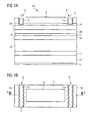
- Figures 1A and 1B a first comparative example of an edge-emitting semiconductor laser is shown.
- Figure 1A shows a cross section along the line AB of in FIG. 1B represented supervision.
- the edge-emitting semiconductor laser has a semiconductor body 10, in which a waveguide region 4 is contained.
- the waveguide region 4 comprises a first waveguide layer 2A and a second waveguide layer 2B, between which an active layer 3 provided for generating laser radiation is arranged.
- the active layer 3 of the edge-emitting semiconductor laser may in particular be a single or multiple quantum well structure.
- the waveguide layers 2A, 2B with the active layer 3 embedded therebetween form the waveguide region 4.
- the waveguide region 4 is is arranged between a first cladding layer 1A and a second cladding layer 1B following the waveguide region 1B in the growth direction of the semiconductor body 10.
- the first cladding layer 1A is arranged on a side facing a substrate 13 of the semiconductor body 10
- the second cladding layer 1B is arranged on a side of the semiconductor body 10 facing away from the substrate 13 from the active layer 3.
- one or more further layers for example a buffer layer 14, may be arranged between the substrate 13 of the semiconductor body 10 and the first cladding layer 1A.
- the electrical contacting of the edge-emitting semiconductor laser is effected, for example, by a first electrical contact layer 8 on an upper side 5 of the semiconductor body 10 and a second electrical contact layer 9 on a rear side of the substrate 13.
- a first electrical contact layer 8 on an upper side 5 of the semiconductor body 10
- a second electrical contact layer 9 on a rear side of the substrate 13.
- Semiconductor layers (not shown) may be arranged.
- the cladding layers 1A, 1B advantageously have a lower refractive index than the waveguide layers 2A, 2B, whereby the laser radiation propagating in the lateral direction is guided essentially in the waveguide region 4.
- the laser modes also extend at least partially into the cladding layers 1A, 1B. Therefore, it is possible to influence the laser modes propagating in the waveguide region 4 by changing the characteristics of the cladding layers 1A, 1B.
- the semiconductor body 10 has phase structures 6 formed in the second cladding layer 1B.
- the phase structure 6 comprises two recesses 7, which extend from the upper side 5 of the semiconductor body 10 into the first cladding layer 1B.
- the phase structure 6 is located in a region of the second cladding layer 1B that is recessed from the first contact layer 8. Alternatively, it would also be possible to arrange the phase structure 6 at least partially below the first contact layer 8.
- the propagation of the laser modes can be influenced in a targeted manner by the phase structures 6, wherein in particular it can be achieved that higher lateral modes have greater circulation losses in the laser resonator arranged between the side facets of the semiconductor body than the lateral fundamental mode of the semiconductor laser.
- the phase structures 6 it is therefore possible in particular to achieve operation of the semiconductor laser in one or more preferred modes, in particular only in the lateral fundamental mode.
- the radiation of the lateral fundamental mode has a low beam divergence. This is particularly advantageous for applications in which the radiation emitted by the semiconductor laser is to be coupled into an optical fiber.
- phase structure 6 can be predicted, taking into account the parameters of the materials of the semiconductor layer sequence, the geometrical dimensions and the wavelength of the emitted radiation such that higher lateral laser modes experience greater circulation losses in the laser resonator formed by the side facets 16 than lower lateral modes, in particular the lateral one Fundamental mode of the semiconductor laser.
- the distance between the respective side facets 16 of the semiconductor laser and the recesses 7 in the second cladding layer 1B, which form the phase structure 6, in the plane of the second cladding layer 1B can take a wavy course, as in the plan view in FIG FIG. 1B is shown.
- the recesses 7, which extend from the upper side of the semiconductor body 5 into the second cladding layer 1B, are advantageously formed by an etching process in the semiconductor body 10.
- semiconductor lasers emitting in the infrared spectral range which are characterized by a high concentration of the laser modes on the waveguide region 4 and / or a comparatively thick second cladding layer 1B, it may be necessary to etch the recesses 7 so deeply into the semiconductor body 10 that they reach into the vicinity of the waveguide region 4.
- the desired etching depth must be achieved as accurately as possible and be well reproducible.
- an intermediate layer 11 is advantageously embedded in the second cladding layer 1B, which consists of a semiconductor material different from the semiconductor material of the second cladding layer 1B.
- the intermediate layer 11 differs in its chemical composition from the second cladding layer 1B and in particular comprises a material of the third or fifth main group of the periodic table, which is not contained in the second cladding layer 1B.
- the second cladding layer 1B may in particular be a layer of Al x Ga 1-x As with 0 ⁇ x ⁇ 1.
- the intermediate layer 11 is advantageously formed of a III-V semiconductor material containing another material of the third or fifth main group as Al, Ga or As.
- the intermediate layer 11 has In or P.
- the material of the intermediate layer 11 may include InGaP, InGaAs or InGaAlP.
- the second cladding layer 1B preferably contains neither In nor P.
- the intermediate layer 11 advantageously functions as an indicator layer during the etching process for achieving a desired etching depth.
- the intermediate layer 11 is thus incorporated into the second cladding layer 1B when the second cladding layer 1B is grown in the depth, up to which the recesses 7 of the phase structure 6 should reach.
- the etching may be carried out by a wet-chemical etching process or by a dry etching process, or a combination of a wet-chemical and a dry-etching process may also be used.
- the intermediate layer 11 may function as an etching stop layer using an etching solution having a larger etch rate for the material of the second cladding layer 1B than for the etching layer Material of the Intermediate Layer 11.
- the detection of an element in the intermediate layer 11, which is not contained in the second cladding layer advantageously serves as an indicator for achieving the desired etching depth.
- a measuring device is used which can detect the occurrence of a chemical element contained only in the intermediate layer 11.
- the element can be detected, and thus the reaching of the intermediate layer 11 can be determined.
- the etching process can be stopped specifically.
- the recesses 7 extend at least into the intermediate layer 11. Preferably, the recesses 7 end in the intermediate layer 11. However, it is also possible that the recesses extend slightly deeper into the semiconductor body 10 than into the intermediate layer 11. This case can be particularly occur when the intermediate layer 11 is comparatively thin and an at least slight time delay occurs between the detection of the characteristic element contained therein and the stopping of the etching process.
- the intermediate layer 11 a layer which is very thin compared to the second cladding layer 1B is preferably used.
- the thickness of the intermediate layer 11 is preferably between 10 nm and 100 nm, more preferably between 20 nm and 50 nm.
- the second cladding layer 1B may have a thickness of, for example, 1 ⁇ m or more. Due to the small thickness of the intermediate layer 11, the propagation of the laser modes is only slightly different from the Intermediate layer 11 influenced. Therefore, it is possible to use for the intermediate layer 11 a material which differs in refractive index from the material of the second cladding layer 1B.
- the phase structure 6 may be at least partially provided with a cover layer 15.
- a cover layer 15 As in Figure 1A illustrated, for example, the side edges and the bottom surface of the recesses 7 may be covered by the cover layer 15. Alternatively, it is also possible that the recesses 7 are partially or completely filled by the cover layer 15.
- the cover layer 7 preferably comprises an electrically insulating material such as, for example, a silicon oxide, a silicon nitride, a silicon oxynitride or benzocyclobutene (BCB).
- the first contact layer 8 of the semiconductor body 10 is preferably designed as a contact strip.
- the contact strip 8 runs with its longitudinal direction perpendicular to the side facets 16 of the semiconductor laser and defines the region in which current for generating laser radiation is impressed into the semiconductor body 10.
- the phase structures 6 may be formed, for example, in an edge region in the vicinity of the side facets 16 of the semiconductor body 10, the contact strip 8 being located between the phase structures 6. But it is also possible that the contact strip 8 extends over the phase structures 6. This may be the case, in particular, when the recesses 7 are filled with a cover layer 15.
- the phase structures may also extend to the side facets 16 of the semiconductor laser.
- the contact strip 8 may be a strip-shaped metallization on the upper side 5 of the semiconductor body 10.
- the upper side 5 of the semiconductor body is provided with a passivation layer, wherein the passivation layer has an opening which defines the contact strip 8 (not shown).
- the passivation layer can be covered over a large area with a metallization such as a gold layer, wherein the contact with the semiconductor body 10 is made only in the region of the opening which defines the contact strip 8.
- the contact strip 8 preferably has a width between 10 .mu.m and 500 .mu.m.
- the edge-emitting semiconductor laser can thus be a wide-band laser.
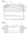
- the second comparative example of an edge-emitting semiconductor laser shown in a cross-section along the line CD of the plan differs from the first comparative example in that the second cladding layer 1B is composed of a first sub-layer 1C and a second sub-layer 1D.
- the first sub-layer 1C adjoins the waveguide region 4 and the second sub-layer 1D is arranged above the first sub-layer 1C.
- the first sub-layer 1C of the second cladding layer 1B has a larger refractive index than the second sub-layer 1D.
- the refractive index of the first sub-layer 1C thus lies between the refractive index of the second waveguide layer 2B and the second sub-layer 1D.
- the first sub-layer 1C of the second cladding layer 1B has a refractive index which is between the refractive index of the second waveguide layer 2A and the refractive index of the second sub-layer 1D of the second cladding layer 1B, it is achieved that a larger proportion of the laser radiation is at least into the first sub-layer 1C of the second cladding layer 1B penetrates, in the case of abrupt change of the refractive index, from the refractive index of the second waveguide layer 2A to the refractive index of the second sublayer 1D of the second cladding layer 1B.
- phase structure on the lateral laser modes which have a comparatively large overlap with the second cladding layer 1B, is advantageously increased in this way.
- This facilitates in particular the use of phase structures in semiconductor lasers with comparatively thick second cladding layers 1B, in particular in semiconductor lasers emitting in the infrared spectral range.
- the intermediate layer 11, which, as in the first exemplary embodiment, serves for the defined adjustment of the depth of the recesses 7 of the phase structures 6, is preferably arranged in the first sub-layer 1C of the second cladding layer 1B. In this way, recesses 7 can be produced, which extend into the adjacent to the waveguide region 4 first sub-layer 1C.
- the second comparative example corresponds to the first comparative example with respect to its mode of operation and the advantageous embodiments.
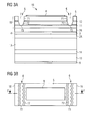
- a second intermediate layer 12 is embedded in the second cladding layer 1B in addition to the first intermediate layer 11.
- the second intermediate layer 12 corresponds to the first intermediate layer 11 described in connection with the first exemplary embodiment.
- the second intermediate layer 12 is advantageously between 10 nm and 100 nm, preferably between 20 nm and 50 nm Thick layer consisting of a semiconductor material different from the semiconductor material of the first cladding layer, which has at least one element of the third or fifth main group not contained in the second cladding layer 1B.
- the embedding of the additional second intermediate layer 12 in the second cladding layer 1B facilitates the fabrication of phase structures 6 having a spatially varying depth in the second cladding layer 1B.
- the recesses 7 extend at their side edges 71 into the second intermediate layer 12 and at its base 73 into the first intermediate layer 11. Between the side edges 71 and the base 73, the recesses 7 oblique side edges 72. In the region of the oblique side flanks 72, the depth of the recesses 7 varies continuously, in particular linearly.
- Such recesses 7 can be produced, for example, that initially until reaching the second intermediate layer 12, which is arranged above the first intermediate layer 11 in the second cladding layer 1B, a first etching process is applied, which produces steep and preferably vertical side edges 71. Subsequently, with a second etching process, the oblique side edges 72 generated further etched to the second intermediate layer 12.
- a wet-chemical etching process can be used as the first etching process
- a dry etching process can be used as the second etching process.
- other variants are conceivable, for example two consecutive wet-chemical etching processes with different etching solutions or two successive dry etching processes.
- phase structures 6 can be produced in which the refractive index difference between the phase structure 6 and the remaining semiconductor body 10 is less abrupt than with recesses having a constant depth.
- coupling losses which may occur when the laser radiation passes from the main region into the phase structure 6 of the semiconductor body 10 are reduced, which advantageously improves the efficiency of the semiconductor laser.
- the embodiment corresponds to the FIGS. 3A and 3B in terms of its operation and the advantageous embodiments of the first comparative example.
- the edge emitting semiconductor laser is a laser bar having a plurality of contact strips 8 at the top 5 of the semiconductor body 10.
- the contact strips 8 run parallel to one another and with their longitudinal direction perpendicular to the side facets 16 of the Semiconductor laser.
- the contact strips 8 are arranged, for example, between the phase structures 6 and the side edges 16 of the semiconductor body 10.
- the semiconductor body 10 and the phase structures 6 contained therein can be designed as in the previously described comparison and exemplary embodiments and will therefore not be explained again in more detail.
- the active layer of the laser bar has therefore a plurality of emission regions, which are each arranged below the contact strips 8. In the illustrated embodiment, the number of contact strips 8 and the emission areas is five.
- the contact strips 8 preferably each have the same width b and the same distance d from each other.
- the width b of the contact strips 8 may be, for example, between 10 microns and 500 microns.
- the distances d of the centers of the contact strips are preferably 0.01 ⁇ b / d ⁇ 0.5.
- the contact strips have a width of 100 ⁇ m, the distance d is at least 200 ⁇ m.
- a laser bar having such a ratio of the widths b to the distances d of the contact strips 8 is particularly well suited for coupling the plurality of emitted laser beams 17 into an optical fiber 18.
- the coupling of the laser beams 17 in the optical fiber 18 can be done with one or more optical elements 19, 20.
- the first optical element 19 may be a microlens array in which each emission region is assigned a microlens, which effects beam shaping of the respective laser beam 17.
- the multiple beams may, for example, with another optical element, such as a lens 20, bundled and coupled into the optical fiber 18.
- the semiconductor body 10 provided with the phase structures 6 is particularly well suited, because a low beam divergence in both the vertical and in the horizontal beam direction can be achieved by the phase structures 6 . It is therefore possible to use comparatively simple optical elements 19, 20 such as, for example, spherical lenses instead of complex aspherical optical elements, or even one or even all the optical elements 19, 20 can be dispensed with.
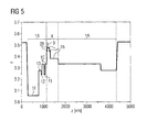
- FIG. 5 schematically shows the profile of the refractive index n in a further embodiment of an edge-emitting semiconductor laser along a location coordinate z, which extends from the top of the semiconductor body in the direction of the substrate.
- the edge-emitting semiconductor laser has a first cladding layer 1A, a second cladding layer 1B, and a waveguide region 4 interposed therebetween.
- the waveguide region 4 comprises an active layer 3, which is a quantum well layer, as well as the first waveguide layer 2A and the second waveguide layer 2B.
- the waveguide layers 2A, 2B and the cladding layers 1A, 1B are each composed of a plurality of sublayers.
- the first cladding layer 1A comprises two partial layers, the first Waveguide layer 2A three sub-layers and the second waveguide layer 2B two sub-layers.
- the second cladding layer 1B has three sub-layers 1C, 1D, 1E.
- the refractive index n gradually increases from the top of the semiconductor body toward the active layer and gradually decreases from the active layer 3 in the direction of the substrate.
- the second cladding layer 1B are embedded two intermediate layers 11, 12 made of a semiconductor material having at least one element of the third or fifth main group not contained in the sub-layers 1C, 1D and 1E of the second cladding layer 1B.
- the sublayers 1C, 1D, 1E of the second cladding layer 1B may comprise Al x Ga 1-x As with 0 ⁇ x ⁇ 1, the intermediate layers 11, 12 including a semiconductor material containing In and / or P such as InGaAs, InGaP or InGaAsP contain.
- the intermediate layers 11, 12 are not considered as partial layers of the second cladding layer 1B.
- the sublayers 1C, 1D, 1E of the second cladding layer have the same constituents, but they can be present in different concentrations.
- the partial layers 1C, 1D, 1E of the second cladding layer 1B may have Al x Ga 1-x As with 0 ⁇ x ⁇ 1, the partial layers having a different aluminum content x.
- the aluminum content may decrease from the top of the second cladding layer 1B toward the active layer 3, so that the refractive index in this direction increases from sub-layer to sub-layer.
- the first intermediate layer 11 is embedded in the first partial layer 1C of the second cladding layer 1B.
- the second intermediate layer 12 is disposed between the first sub-layer 1C and the second sub-layer 1D.
- the two intermediate layers 11, 12 embedded in the second cladding layer 1B facilitate the production of phase structures having recesses with variable depth, as previously described in connection with FIGS FIGS. 3A and 3B described.
- the second waveguide layer 2B thinner than the first waveguide layer 2A.
- the second waveguide layer 2B has only half the thickness, more preferably only one fifth or even only one tenth of the thickness of the first waveguide layer 2A.
Description
Die Erfindung betrifft einen kantenemittierenden Halbleiterlaser mit einem Phasenstrukturbereich zur Selektion lateraler Lasermoden.The invention relates to an edge emitting semiconductor laser having a phase structure region for the selection of lateral laser modes.
Diese Patentanmeldung beansprucht die Priorität der deutschen Patentanmeldungen
Kantenemittierende Halbleiterlaser für hohe Ausgangsleistungen werden meist als Breitstreifenlaser ausgeführt, bei denen der aktive Bereich eine Breite von beispielsweise 100 µm oder mehr aufweisen kann. Wegen der vergleichsweise großen lateralen Ausdehnung des aktiven Bereichs können bei derartigen Halbleiterlasern in der Regel viele laterale Lasermoden anschwingen. Ein Multimode-Betrieb eines kantenemittierenden Halbleiterlasers erschwert insbesondere die Einkopplung des emittierten Laserlichts in nachfolgende optische Elemente, beispielsweise in Lichtleiter.Edge-emitting semiconductor lasers for high output powers are usually designed as wide-band lasers, in which the active region can have a width of, for example, 100 μm or more. Because of the comparatively large lateral extent of the active region, in the case of such semiconductor lasers, as a rule, many lateral laser modes can oscillate. A multi-mode operation of an edge-emitting semiconductor laser makes it particularly difficult to couple the emitted laser light into subsequent optical elements, for example into optical fibers.
Zur Unterdrückung höherer lateraler Lasermoden, insbesondere zum Erzielen eines Betriebs in der lateralen Grundmode, ist aus der Druckschrift
Die für im sichtbaren Spektralbereich emittierende Halbleiterlaser an sich bekannten Phasenstrukturen lassen sich nicht ohne weiteres auf im infraroten Spektralbereich emittierende Halbleiterlaser übertragen. Dies beruht darauf, dass die Laserstrahlung bei Halbleiterlasern im infraroten Spektralbereich stärker auf den Wellenleiterbereich konzentriert ist und weniger stark in die Mantelschichten eindringt als bei Halbleiterlasern im sichtbaren Spektralbereich. Zudem sind die Mantelschichten bei Halbleiterlasern im infraroten Spektralbereich aufgrund der vergleichsweise großen Wellenlänge verhältnismäßig dick. Aus diesem Grund ist die Wirkung von Phasenstrukturen mit geringen Ätztiefen in der zweiten Mantelschicht nur sehr gering. Andererseits zeigt sich eine starke Abhängigkeit der Wirkung von Phasenstrukturen von der Ätztiefe, wenn bis in die Nähe des Wellenleiterbereichs geätzt wird. Zur Realisierung von Phasenstrukturen für Halbleiterlaser im infraroten Spektralbereich wäre es also erforderlich, vergleichsweise tiefe Ätzstrukturen in dem Halbleiterkörper zu erzeugen, deren Tiefe sehr genau definiert sind. Beide Anforderungen lassen sich aber nur schwer gleichzeitig erfüllen.The phase structures known per se for the semiconductor laser emitting in the visible spectral range can not readily be transferred to semiconductor lasers emitting in the infrared spectral range. This is based on the fact that the laser radiation is more concentrated on the waveguide region in semiconductor lasers in the infrared spectral range and less penetrates into the cladding layers than semiconductor lasers in the visible spectral range. In addition, the cladding layers are relatively thick in semiconductor lasers in the infrared spectral range due to the comparatively large wavelength. For this reason, the effect of phase structures with low etch depths in the second cladding layer is only very small. On the other hand, a strong dependence of the effect of phase structures on the etch depth is observed when etching close to the waveguide region. For the realization of phase structures for semiconductor lasers in the infrared spectral range, it would therefore be necessary To produce comparatively deep etching structures in the semiconductor body, the depth of which are defined very precisely. Both requirements are difficult to meet simultaneously.
Die Druckschrift
Die Druckschrift
Eine Aufgabe besteht darin, einen kantenemittierenden Halbleiterlaser anzugeben, der eine Halbleiterschichtenfolge aufweist, welche die Herstellung von Phasenstrukturen mit variierender Tiefe vereinfacht, wobei die Phasenstrukturen insbesondere auch für Halbleiterlaser im infraroten Spektralbereich zu realisieren sind.One object is to provide an edge-emitting semiconductor laser which has a semiconductor layer sequence which simplifies the production of phase structures with varying depth, wherein the phase structures are to be realized in particular also for semiconductor lasers in the infrared spectral range.
Diese Aufgabe wird durch einen kantenemittierenden Halbleiterlaser mit den Merkmalen des unabhängigen Anspruchs 1 gelöst. Vorteilhafte Ausgestaltungen und Weiterbildungen der Erfindung sind Gegenstand der abhängigen Ansprüche.This object is achieved by an edge emitting semiconductor laser having the features of
Gemäß zumindest einer Ausführungsform der Erfindung enthält ein kantenemittierender Halbleiterlaser einen Halbleiterkörper mit einem Wellenleiterbereich, wobei der Wellenleiterbereich eine erste Wellenleiterschicht, eine zweite Wellenleiterschicht und eine zwischen der ersten Wellenleiterschicht und der zweiten Wellenleiterschicht angeordnete aktive Schicht zur Erzeugung von Laserstrahlung aufweist. In der aktiven Schicht des Halbleiterkörpers wird im Betrieb des Halbleiterlasers elektromagnetische Strahlung erzeugt und verstärkt. Beispielsweise beinhaltet die aktive Schicht einen oder mehrere Quantentöpfe, Quantendrähte oder Quantenpunkte.According to at least one embodiment of the invention, an edge emitting semiconductor laser includes a semiconductor body having a waveguide region, wherein the waveguide region comprises a first waveguide layer, a second waveguide layer, and an active layer for generating laser radiation disposed between the first waveguide layer and the second waveguide layer. In the active layer of the semiconductor body electromagnetic radiation is generated and amplified during operation of the semiconductor laser. For example, the active layer includes one or more quantum wells, quantum wires, or quantum dots.
Der Wellenleiterbereich ist zwischen einer ersten Mantelschicht und einer dem Wellenleiterbereich in Wachstumsrichtung des Halbleiterkörpers nachfolgenden zweiten Mantelschicht angeordnet. Die erste und zweite Mantelschicht weisen vorteilhaft einen geringeren Brechungsindex als die Wellenleiterschichten auf. Aufgrund des Brechungsindexunterschieds zwischen dem Wellenleiterbereich und den Mantelschichten ist das Modenprofil stark auf den Wellenleiterbereich konzentriert. Dennoch dringen die Lasermoden zumindest geringfügig in die Mantelschichten ein.The waveguide region is arranged between a first cladding layer and a second cladding layer following the waveguide region in the growth direction of the semiconductor body. The first and second cladding layers advantageously have a lower refractive index than the waveguide layers. Due to the refractive index difference between the waveguide region and the cladding layers, the mode profile is highly concentrated on the waveguide region. Nevertheless, the laser modes penetrate at least slightly into the cladding layers.
In dem Halbleiterkörper ist vorteilhaft eine Phasenstruktur zur Selektion lateraler Moden der von der aktiven Schicht emittierten Laserstrahlung ausgebildet, wobei die Phasenstruktur mindestens eine Ausnehmung umfasst, die sich von einer Oberfläche des Halbleiterkörpers in die zweite Mantelschicht hinein erstreckt. Die Phasenstruktur ist vorzugsweise derart ausgebildet, dass die laterale Grundmode der Laserstrahlung geringere Verluste als die Strahlung höherer Lasermoden erfährt. Aufgrund der Phasenstruktur erfährt die Laserstrahlung, die sich in dem Wellenleiterbereich ausbreitet, Umlaufverluste, wobei der strukturierte Bereich derart ausgebildet ist, dass höhere Lasermoden stärker gedämpft werden als die laterale Grundmode. Auf diese Weise kann insbesondere erreicht werden, dass beim Betrieb des Halbleiterlasers nur eine oder wenige bevorzugte Lasermoden, vorzugsweise nur die laterale Grundmode, anschwingen.A phase structure for selecting lateral modes of the laser radiation emitted by the active layer is advantageously formed in the semiconductor body, wherein the phase structure comprises at least one recess which extends from a surface of the semiconductor body into the second cladding layer. The phase structure is preferably designed such that the lateral fundamental mode of the laser radiation experiences lower losses than the radiation of higher laser modes. Due to the phase structure The laser radiation propagating in the waveguide region undergoes circulation losses, the structured region being designed in such a way that higher laser modes are attenuated more strongly than the lateral fundamental mode. In this way, it can be achieved, in particular, that during operation of the semiconductor laser only one or a few preferred laser modes, preferably only the lateral fundamental mode, oscillate.
Dadurch, dass höhere Moden der Laserstrahlung unterdrückt werden und vorzugsweise nur die laterale Grundmode anschwingt, wird eine hohe Strahlqualität des kantenemittierenden Halbleiterlasers erzielt. Insbesondere eignet sich das Strahlprofil der lateralen Grundmode gut für eine Strahlformung mit optischen Elementen und insbesondere für die hocheffiziente Einkopplung in eine Lichtleitfaser.Because higher modes of the laser radiation are suppressed and preferably only the lateral fundamental mode oscillates, a high beam quality of the edge-emitting semiconductor laser is achieved. In particular, the beam profile of the lateral fundamental mode is well suited for beam shaping with optical elements and in particular for the highly efficient coupling into an optical fiber.
In die zweite Mantelschicht ist mindestens eine Zwischenschicht aus einem von dem Halbleitermaterial der zweiten Mantelschicht verschiedenen Halbleitermaterial eingebettet. Die mindestens eine Ausnehmung, welche die Phasenstruktur ausbildet, erstreckt sich von der Oberseite des Halbleiterkörpers zumindest teilweise bis in die Zwischenschicht.At least one intermediate layer of a semiconductor material different from the semiconductor material of the second cladding layer is embedded in the second cladding layer. The at least one recess, which forms the phase structure, extends from the upper side of the semiconductor body at least partially into the intermediate layer.
Das Erzeugen der Phasenstruktur durch Ausbildung von einer oder mehreren Ausnehmungen in dem Halbleiterkörper kann insbesondere mit einem Ätzprozess erfolgen, bei dem die zweite Mantelschicht teilweise abgetragen wird. Bei dem Ätzprozess kann es sich um einen nasschemischen Ätzprozess oder um einen Trockenätzprozess handeln. Die in die zweite Mantelschicht eingebettete Zwischenschicht fungiert vorteilhaft als Indikatorschicht für das Erreichen einer gewünschten Ätztiefe und erleichtert auf diese Weise die gezielte und reproduzierbare Herstellung von Ausnehmungen mit definierter Tiefe. Die in die zweite Mantelschicht eingebettete Zwischenschicht kann bei nasschemischer Ätzung des Halbleiterkörpers, insbesondere der zweiten Mantelschicht, als Ätzstoppschicht verwendet werden. In diesem Fall wird für die Zwischenschicht ein Halbleitermaterial verwendet, das für die verwendete Ätzlösung eine geringere Ätzrate als die zweite Mantelschicht aufweist.The generation of the phase structure by forming one or more recesses in the semiconductor body can be carried out in particular with an etching process in which the second cladding layer is partially removed. The etching process may be a wet chemical etching process or a dry etching process. The interlayer embedded in the second cladding layer advantageously functions as an indicator layer for achieving a desired etching depth and facilitates in this way the targeted and reproducible production of recesses with a defined depth. The intermediate layer embedded in the second cladding layer can be used as an etching stop layer in wet-chemical etching of the semiconductor body, in particular of the second cladding layer. In this case, a semiconductor material is used for the intermediate layer, which has a lower etching rate than the second cladding layer for the etching solution used.
Wenn ein Trockenätzprozess wie beispielsweise eine Plasmaätzung zur Herstellung der einen oder mehreren Ausnehmungen in dem Halbleiterkörper verwendet wird, kann mittels Überwachung der optischen Emission des Plasmas in der Prozesskammer während des Ätzprozesses auf das Erreichen der Zwischenschicht geschlossen und an dieser Stelle der Ätzprozess gestoppt werden. Um eine besonders homogene und definierte Ätztiefe zu erzielen, ist es in diesem Fall vorteilhaft, wenn die Zwischenschicht bei dem Plasmaätzprozess eine geringere Ätzrate als die zweite Mantelschicht aufweist.If a dry etch process, such as plasma etching, is used to fabricate the one or more cavities in the semiconductor body, then monitoring the optical emission of the plasma in the process chamber during the etch process may conclude that the interlayer has been reached and, at that location, stop the etch process. In order to achieve a particularly homogeneous and defined etching depth, it is advantageous in this case if the intermediate layer has a lower etch rate than the second cladding layer in the plasma etching process.
Bei einer bevorzugten Ausführungsform ist das Halbleitermaterial der Zwischenschicht ein III-V-Halbleitermaterial, das mindestens ein Element der dritten oder fünften Hauptgruppe des Periodensystems enthält, das in der zweiten Mantelschicht nicht enthalten ist. Die zweite Mantelschicht enthält vorzugsweise ein III-V-Halbleitermaterial wie insbesondere AlxGa1-xAs mit 0 ≤ x ≤ 1, bevorzugt mit 0 < x < 1. Das Halbeleitermaterial der zweiten Mantelschicht enthält vorzugsweise außer Al, Ga und As keine weiteren Hauptbestandteile, abgesehen von einem oder mehreren Dotierstoffen oder eventuellen Verunreinigungen. Die Zwischenschicht enthält vorzugsweise ein Halbleitermaterial, welches In und/oder P enthält.In a preferred embodiment, the semiconductor material of the intermediate layer is a III-V semiconductor material containing at least one element of the third or fifth main group of the periodic table, which is not contained in the second cladding layer. The second cladding layer preferably contains a III-V semiconductor material such as in particular Al x Ga 1-x As with 0 ≦ x ≦ 1, preferably with 0 <x <1. The half-conductor material of the second cladding layer preferably contains no further than Al, Ga and As Main ingredients, apart from one or more Dopants or possible impurities. The intermediate layer preferably contains a semiconductor material which contains In and / or P.
Das Halbleitermaterial der mindestens einen Zwischenschicht wird bevorzugt derart gewählt, dass es gitterangepasst an die umgebenden Halbleiterschichten ist. Weiterhin ist es vorteilhaft, wenn die für den Leitungstyp der Zwischenschicht relevante Bandkante, das heißt auf der p-Seite der aktiven Zone das Valenzband und auf der n-Seite das Leitungsband, im Wesentlichen mit der umgebenden zweiten Mantelschicht übereinstimmt.The semiconductor material of the at least one intermediate layer is preferably selected such that it is lattice-matched to the surrounding semiconductor layers. Furthermore, it is advantageous if the band edge relevant for the conductivity type of the intermediate layer, that is, the valence band on the p-side of the active zone and the conduction band on the n-side, essentially coincide with the surrounding second cladding layer.
Gemäß einer bevorzugten Ausführungsform weist die Zwischenschicht eine Dicke zwischen einschließlich 10 nm und einschließlich 100 nm auf. Besonders bevorzugt beträgt die Dicke der Zwischenschicht zwischen einschließlich 20 nm und einschließlich 50 nm. Bei einer derart geringen Dicke hat die Zwischenschicht nur einen geringen Einfluss auf die sich im Halbleiterkörper ausbreitenden Lasermoden. Für die Zwischenschicht kann daher vorteilhaft auch ein Halbleitermaterial verwendet werden, dessen Brechzahl nicht notwendigerweise an die Brechzahl der umgebenden zweiten Mantelschicht angepasst sein muss.According to a preferred embodiment, the intermediate layer has a thickness of between 10 nm and 100 nm inclusive. Particularly preferably, the thickness of the intermediate layer is between 20 nm and 50 nm inclusive. With such a small thickness, the intermediate layer has only a small influence on the laser modes propagating in the semiconductor body. For the intermediate layer, it is therefore also advantageously possible to use a semiconductor material whose refractive index does not necessarily have to be adapted to the refractive index of the surrounding second cladding layer.
In die zweite Mantelschicht ist mindestens eine weitere Zwischenschicht eingebettet, wobei sich die Ausnehmung zumindest teilweise bis in die zweite Zwischenschicht hinein erstreckt. Die zweite Zwischenschicht ist von der Oberfläche des Halbleiterkörpers aus gesehen in einer anderen Tiefe angeordnet als die erste Zwischenschicht. Die zweite Zwischenschicht fungiert vorteilhaft als Indikatorschicht für das Erreichen einer zweiten Ätztiefe, die von einer ersten Ätztiefe verschieden ist, für die die erste Zwischenschicht als Indikatorschicht fungiert. Die zweite Mantelschicht ist also vorzugsweise an mindestens einem Punkt bis in die erste Zwischenschicht abgetragen und an mindestens einem weiteren Punkt bis in die zweite Zwischenschicht abgetragen.At least one further intermediate layer is embedded in the second cladding layer, the recess extending at least partially into the second interlayer. The second intermediate layer is arranged at a different depth from the surface of the semiconductor body than the first intermediate layer. The second interlayer advantageously functions as an indicator layer for achieving a second etch depth, starting from a first etch depth Etching depth is different, for which the first intermediate layer acts as an indicator layer. The second cladding layer is thus preferably removed at at least one point into the first intermediate layer and removed at at least one further point into the second intermediate layer.
Die Ausnehmung erstreckt sich an mindestens einem ersten Punkt bis in die erste Zwischenschicht und an mindestens einem zweiten Punkt bis in die zweite Zwischenschicht. Dabei weist die Ausnehmung zwischen dem ersten Punkt und dem zweiten Punkt eine räumlich variierende Tiefe auf. Die Tiefe der mindestens einen Ausnehmung und somit die Dicke der zweiten Mantelschicht kann beispielsweise zwischen dem ersten Punkt und dem zweiten Punkt kontinuierlich, vorzugsweise linear, zunehmen oder abnehmen. Alternativ kann die Tiefe der Ausnehmung auch stufenförmig in mehreren Stufen zunehmen oder abnehmen. Durch die räumlich variierende Tiefe der Ausnehmung werden abrupte Änderungen des Brechungsindex zwischen der Phasenstruktur und dem Hauptbereich des Halbleiterkörpers verringert. Auf diese Weise werden Koppelverluste, die beim Übertritt der Laserstrahlung von dem Hauptbereich in den Phasenstrukturbereich des Halbleiterkörpers auftreten können, verringert, wodurch sich vorteilhaft die Effizienz des Halbleiterlasers verbessert.The recess extends at at least one first point into the first intermediate layer and at least one second point into the second intermediate layer. In this case, the recess between the first point and the second point has a spatially varying depth. The depth of the at least one recess and thus the thickness of the second cladding layer may, for example, increase or decrease continuously, preferably linearly, between the first point and the second point. Alternatively, the depth of the recess can also increase or decrease stepwise in several stages. The spatially varying depth of the recess reduces abrupt changes in the refractive index between the phase structure and the main region of the semiconductor body. In this way, coupling losses, which can occur when the laser radiation passes from the main region into the phase structure region of the semiconductor body, are reduced, which advantageously improves the efficiency of the semiconductor laser.
Bei einer weiteren vorteilhaften Ausgestaltung weist die zweite Mantelschicht eine erste Teilschicht, die an den Wellenleiterbereich angrenzt, und eine zweite Teilschicht, die an die erste Teilschicht angrenzt, auf, wobei die erste Teilschicht einen größeren Brechungsindex als die zweite Teilschicht aufweist. Dabei wird die mindestens eine Zwischenschicht, die in die zweite Mantelschicht eingebettet ist, nicht als erste oder zweite Teilschicht der Mantelschicht betrachtet. Im Fall einer aus zwei Teilschichten zusammengesetzten zweiten Mantelschicht ist die mindestens eine Zwischenschicht also in die erste oder in die zweite Teilschicht eingebettet.In a further advantageous refinement, the second cladding layer has a first sublayer adjoining the waveguide region and a second sublayer adjoining the first sublayer, wherein the first sublayer has a greater refractive index than the second sublayer. In this case, the at least one intermediate layer which is embedded in the second cladding layer, not as the first or second sub-layer of Considered cladding layer. In the case of a second cladding layer composed of two sublayers, the at least one interlayer is thus embedded in the first or in the second sublayer.
Bevorzugt ist die mindestens eine Zwischenschicht in die erste Teilschicht der zweiten Mantelschicht eingebettet. Die erste Teilschicht der zweiten Mantelschicht weist einen Brechungsindex auf, der zwischen den Brechungsindices der zweiten Wellenleiterschicht und der zweiten Teilschicht der zweiten Mantelschicht liegt. Der Brechungsindex nimmt also abgesehen von der mindestens einen eingebetteten Zwischenschicht von der zweiten Wellenleiterschicht zur nachfolgenden ersten Teilschicht der zweiten Mantelschicht und zur zweiten Teilschicht der zweiten Mantelschicht stufenförmig ab. Auf diese Weise kann erreicht werden, dass der Brechungsindexsprung von der zweiten Wellenleiterschicht zur zweiten Mantelschicht weniger abrupt ist, als wenn eine zweite Mantelschicht mit dem Brechungsindex der zweiten Teilschicht direkt an die zweite Wellenleiterschicht angrenzen würde.Preferably, the at least one intermediate layer is embedded in the first sub-layer of the second cladding layer. The first sub-layer of the second cladding layer has a refractive index which lies between the refractive indices of the second waveguide layer and the second sub-layer of the second cladding layer. Apart from the at least one embedded intermediate layer, the refractive index therefore decreases in steps from the second waveguide layer to the subsequent first sublayer of the second cladding layer and to the second sublayer of the second cladding layer. In this way it can be achieved that the refractive index jump from the second waveguide layer to the second cladding layer is less abrupt than if a second cladding layer with the refractive index of the second sublayer would directly adjoin the second waveguide layer.
Dadurch, dass die erste Teilschicht der zweiten Mantelschicht einen Brechungsindex aufweist, der zwischen dem Brechungsindex der zweiten Wellenleiterschicht und dem Brechungsindex der zweiten Teilschicht der zweiten Mantelschicht liegt, wird erreicht, dass ein größerer Anteil der Laserstrahlung zumindest in die erste Teilschicht der zweiten Mantelschicht eindringt als im Fall einer abrupten Änderung des Brechungsindex von dem Brechungsindex der zweiten Wellenleiterschicht zum Brechungsindex der zweiten Teilschicht der zweiten Mantelschicht. Die Wirkung einer Phasenstruktur auf die lateralen Lasermoden, die einen vergleichsweise großen Überlapp mit der zweiten Mantelschicht aufweisen, wird auf diese Weise vorteilhaft erhöht. Dies erleichtert insbesondere den Einsatz von Phasenstrukturen in Halbleiterlasern mit vergleichsweise dicken zweiten Mantelschichten, insbesondere in im infraroten Spektralbereich emittierenden Halbleiterlasern.Due to the fact that the first sub-layer of the second cladding layer has a refractive index which is between the refractive index of the second waveguide layer and the refractive index of the second sub-layer of the second cladding layer, it is achieved that a larger proportion of the laser radiation penetrates at least into the first sub-layer of the second cladding layer in the case of an abrupt change of the refractive index from the refractive index of the second waveguide layer to the refractive index of the second sublayer of the second cladding layer. The effect of a phase structure on the lateral laser modes, the one Having comparatively large overlap with the second cladding layer is advantageously increased in this way. This facilitates in particular the use of phase structures in semiconductor lasers with comparatively thick second cladding layers, in particular in semiconductor lasers emitting in the infrared spectral range.
Es ist auch möglich, dass die zweite Mantelschicht mehr als nur zwei Teilschichten aufweist. Insbesondere kann die zweite Mantelschicht mehrere Teilschichten aufweisen, deren Brechungsindex in Wachstumsrichtung des Halbleiterkörpers von der zweiten Wellenleiterschicht aus stufenförmig abnimmt. Alternativ kann die zweite Mantelschicht auch einen Brechungsindexgradienten aufweisen, wobei der Brechungsindex in Wachstumsrichtung kontinuierlich abnimmt.It is also possible for the second cladding layer to have more than just two sublayers. In particular, the second cladding layer may have a plurality of sublayers whose refractive index decreases stepwise in the growth direction of the semiconductor body from the second waveguide layer. Alternatively, the second cladding layer may also have a refractive index gradient, the refractive index decreasing continuously in the direction of growth.
Weiterhin ist es auch möglich, dass auch die erste Mantelschicht, die in Wachstumsrichtung des Halbleiterkörpers unterhalb des Wellenleiterbereichs angeordnet ist, aus zwei oder mehreren Teilschichten zusammengesetzt ist. Beispielsweise kann die erste Mantelschicht eine an die erste Wellenleiterschicht angrenzende erste Teilschicht, die einen geringeren Brechungsindex als die erste Wellenleiterschicht aufweist, und eine zweite Teilschicht, die einen geringeren Brechungsindex als die erste Teilschicht aufweist, enthalten. Der Brechungsindex nimmt also von der ersten Wellenleiterschicht zur zweiten Teilschicht der ersten Mantelschicht hin stufenweise ab.Furthermore, it is also possible for the first cladding layer, which is arranged below the waveguide region in the growth direction of the semiconductor body, to be composed of two or more sublayers. By way of example, the first cladding layer may include a first sublayer adjacent to the first waveguide layer, which has a lower refractive index than the first waveguide layer, and a second sublayer, which has a lower refractive index than the first sublayer. The refractive index thus decreases gradually from the first waveguide layer to the second sublayer of the first cladding layer.
Bei einer weiteren vorteilhaften Ausgestaltung ist die Phasenstruktur mit einer Deckschicht versehen. Die Ausnehmungen, welche die Phasenstruktur ausbilden, sind beispielsweise ganz oder teilweise von dem Material der Deckschicht aufgefüllt. Insbesondere ist es auch möglich, dass die Ausnehmungen der Phasenstruktur von der Deckschicht vollständig planarisiert werden.In a further advantageous embodiment, the phase structure is provided with a cover layer. The recesses which form the phase structure are, for example, wholly or partly of the material of Topcoat filled. In particular, it is also possible that the recesses of the phase structure are completely planarized by the cover layer.
Bei der Deckschicht kann es sich insbesondere um eine Passivierungsschicht handeln, die zum Beispiel ein Siliziumoxid, ein Siliziumnitrid, ein Siliziumoxinitrid, ein Aluminiumoxid, Zinkselenid, Germanium oder Benzocyclobuten (BCB) enthalten kann. Die Deckschicht weist vorzugsweise einen Brechungsindex auf, der kleiner ist als der Brechungsindex der zweiten Mantelschicht. Dadurch, dass die Deckschicht einen Brechungsindex zwischen dem Brechungsindex von Luft und dem Brechungsindex des Halbleitermaterials der zweiten Mantelschicht aufweist, wird der Brechungsindexsprung an den Grenzflächen der Ausnehmungen gegenüber nur mit Luft gefüllten Ausnehmungen verringert. Auf diese Weise werden Koppelverluste an den Grenzflächen der Ausnehmungen vermindert.In particular, the capping layer may be a passivation layer, which may contain, for example, a silicon oxide, a silicon nitride, a silicon oxynitride, an aluminum oxide, zinc selenide, germanium or benzocyclobutene (BCB). The cover layer preferably has a refractive index which is smaller than the refractive index of the second cladding layer. By virtue of the cover layer having a refractive index between the refractive index of air and the refractive index of the semiconductor material of the second cladding layer, the refractive index jump at the boundary surfaces of the recesses is reduced in comparison with recesses filled only with air. In this way coupling losses are reduced at the interfaces of the recesses.
Alternativ ist es aber auch möglich, dass die Phasenstruktur mit einer Deckschicht versehen wird, die einen größeren Brechungsindex als das Halbleitermaterial aufweist. In diesem Fall kann die Deckschicht beispielsweise Germanium enthalten.Alternatively, it is also possible that the phase structure is provided with a cover layer having a higher refractive index than the semiconductor material. In this case, the cover layer may contain germanium, for example.
Bei einer vorteilhaften Ausgestaltung ist auf eine Oberfläche des Halbleiterlasers mindestens ein Kontaktstreifen aufgebracht. Der Kontaktstreifen ist vorzugsweise an der Oberseite des Halbleiterkörpers angeordnet. Bei dem Kontaktstreifen kann es sich um eine Elektrode handeln, über die elektrischer Strom in den Halbleiterkörper eingeprägt werden kann. Diese kann zum Beispiel als streifenförmige Metallisierung auf die Oberseite des Halbleiterkörpers aufgebracht sein. Darüber hinaus ist es auch möglich, dass der Kontaktstreifen mittels eines streifenförmigen Durchbruchs in einer Passivierungsschicht auf der Oberseite des Halbleiterkörpers definiert ist. Auf diese Passivierung kann eine Metallschicht großflächig aufgebracht sein. Die Metallschicht befindet sich dann nur im Bereich des Durchbruchs in Kontakt mit dem Halbleiterkörper.In an advantageous embodiment, at least one contact strip is applied to a surface of the semiconductor laser. The contact strip is preferably arranged on the upper side of the semiconductor body. The contact strip can be an electrode via which electrical current can be impressed into the semiconductor body. This can be applied for example as a strip-shaped metallization on the top of the semiconductor body. In addition, it is also possible that the contact strip is defined by means of a strip-shaped opening in a passivation layer on the upper side of the semiconductor body. On this passivation, a metal layer can be applied over a large area. The metal layer is then only in the region of the opening in contact with the semiconductor body.
Mittels des eingeprägten elektrischen Stroms wird in der aktiven Schicht des Halbleiterkörpers elektromagnetische Strahlung erzeugt. Bei dem kantenemittierenden Halbleiterlaser handelt es sich also um einen elektrisch gepumpten Halbleiterlaser.By means of the impressed electrical current, electromagnetic radiation is generated in the active layer of the semiconductor body. The edge-emitting semiconductor laser is thus an electrically pumped semiconductor laser.
Die elektromagnetische Strahlung wird in der aktiven Zone unterhalb des Kontaktstreifens erzeugt. Dort befindet sich also der Emissionsbereich des Halbleiterlasers. Weist der Halbleiterlaser mehrere Kontaktstreifen an der Oberseite des Halbleiterkörpers auf, so wird unterhalb eines jeden Kontaktstreifens Laserstrahlung erzeugt. Der Halbleiterlaser weist dann mehrere Emissionsbereiche auf, deren Zahl der Anzahl der Kontaktstreifen auf der Oberseite entspricht. Der mindestens eine Kontaktstreifen erstreckt sich vorzugsweise entlang der Hauptstrahlrichtung der in der aktiven Zone erzeugten elektromagnetischen Strahlung. Die Haupterstreckungsrichtung des Kontaktstreifens ist dann parallel zur Hauptstrahlrichtung des Emitters, der dem Kontaktstreifen zugeordnet ist. Beispielsweise erstreckt sich der Kontaktstreifen als Streifen gleichmäßiger Breite entlang der Hauptstrahlrichtung der im Halbleiterkörper erzeugten elektromagnetischen Strahlung.The electromagnetic radiation is generated in the active zone below the contact strip. There is thus the emission range of the semiconductor laser. If the semiconductor laser has a plurality of contact strips on the upper side of the semiconductor body, then laser radiation is generated below each contact strip. The semiconductor laser then has a plurality of emission regions whose number corresponds to the number of contact strips on the upper side. The at least one contact strip preferably extends along the main radiation direction of the electromagnetic radiation generated in the active zone. The main extension direction of the contact strip is then parallel to the main radiation direction of the emitter, which is assigned to the contact strip. For example, the contact strip extends as a strip of uniform width along the main radiation direction of the electromagnetic radiation generated in the semiconductor body.
Der mindestens eine Kontaktstreifen des kantenemittierenden Halbleiterlasers weist vorteilhaft eine Breite zwischen einschließlich 10 µm und einschließlich 500 µm auf. Insbesondere handelt es sich bei dem kantenemittierenden Halbleiterlaser also um einen so genannten Breitstreifenlaser.The at least one contact strip of the edge-emitting semiconductor laser advantageously has a width between including 10 μm and including 500 μm. In particular, the edge-emitting semiconductor laser is therefore a so-called wide-band laser.
Bei einer bevorzugten Ausführungsform weist der kantenemittierende Halbleiterlaser mehrere Kontaktstreifen an der Oberfläche auf. Die mehreren Kontaktstreifen sind bevorzugt parallel zueinander auf der Oberfläche des Halbleiterkörpers angeordnet und vorteilhaft in jeweils gleichen Abständen zueinander angeordnet. Bei dem kantenemittierenden Halbleiterlaser handelt es sich in diesem Fall um einen so genannten Laserbarren.In a preferred embodiment, the edge-emitting semiconductor laser has a plurality of contact strips on the surface. The plurality of contact strips are preferably arranged parallel to one another on the surface of the semiconductor body and are advantageously arranged at equal distances from each other. The edge-emitting semiconductor laser in this case is a so-called laser bar.
Bevorzugt weisen die Kontaktstreifen des Halbleiterlasers einen Abstand d und eine Breite b auf, wobei gilt: 0,01 ≤ b/d ≤ 0,5. Der Abstand der Kontaktstreifen untereinander ist in diesem Fall also mindestens doppelt so groß wie die Breite der Kontaktstreifen. Bei einem derartigen Halbleiterlaser ist es besonders vorteilhaft, mittels der Phasenstruktur einen Betrieb in der lateralen Grundmode und eine geringe Strahldivergenz zu erzielen, um die voneinander beabstandeten emittierten Laserstrahlen in eine oder mehrere Lichtleitfasern einkoppeln zu können. Beispielsweise kann ein Lasersystem den hierin beschriebenen kantenemittierenden Halbleiterlaser und mindestens eine Lichtleitfaser umfassen, wobei der Halbleiterlaser einen oder mehrere Laserstrahlen emittiert, die mittels eines oder mehrerer optischer Elemente, die zwischen dem Halbleiterlaser und der Lichtleitfaser angeordnet sind, in die Lichtleitfaser eingekoppelt werden.The contact strips of the semiconductor laser preferably have a spacing d and a width b, where: 0.01 ≦ b / d ≦ 0.5. The distance between the contact strips with each other is in this case at least twice as large as the width of the contact strips. In such a semiconductor laser, it is particularly advantageous to achieve an operation in the lateral fundamental mode and a low beam divergence by means of the phase structure, in order to be able to couple the spaced-apart emitted laser beams into one or more optical fibers. For example, a laser system may include the edge-emitting semiconductor laser described herein and at least one optical fiber, wherein the semiconductor laser emits one or more laser beams coupled into the optical fiber by one or more optical elements disposed between the semiconductor laser and the optical fiber.
Bei dem Halbleiterlaser kann es sich insbesondere um einen im infraroten Spektralbereich emittierenden Halbleiterlaser handeln. Vorzugsweise weist der Halbleiterlaser eine Emissionswellenlänge zwischen 780 nm und 1500 nm auf.The semiconductor laser may, in particular, be a semiconductor laser emitting in the infrared spectral range. Preferably, the semiconductor laser has an emission wavelength between 780 nm and 1500 nm.
Die Erfindung wird im Folgenden anhand von Vergleichsbeispielen und Ausführungsbeispielen in Zusammenhang mit den
Es zeigen:
-
Figur 1A -
Figur 1BFigur 1A -
Figur 2A -
Figur 2BFigur 2A -
Figur 3A eine schematische Darstellung eines Querschnitts durch ein Ausführungsbeispiel eines kantenemittierenden Halbleiterlasers, -
Figur 3B eine schematische Darstellung einer Aufsicht auf das inFigur 3A dargestellte Ausführungsbeispiel, -
Figur 4 -
Figur 5
-
Figure 1A FIG. 2 a schematic representation of a cross section through a comparative example of an edge-emitting semiconductor laser, FIG. -
FIG. 1B a schematic representation of a plan view of the inFigure 1A illustrated comparative example, -
FIG. 2A FIG. 2 shows a schematic illustration of a cross section through a further comparative example of an edge-emitting semiconductor laser, FIG. -
FIG. 2B a schematic representation of a plan view of the inFIG. 2A illustrated comparative example, -
FIG. 3A FIG. 2 a schematic representation of a cross section through an embodiment of an edge-emitting semiconductor laser, FIG. -
FIG. 3B a schematic representation of a plan view of the inFIG. 3A illustrated embodiment, -
FIG. 4 a schematic representation of a plan view of another embodiment of an edge-emitting semiconductor laser, and -
FIG. 5 a graphical representation of the course of the refractive index n in the vertical direction z in the semiconductor body in another embodiment of an edge-emitting semiconductor laser.
Gleiche oder gleich wirkende Bestandteile sind in den Figuren mit den gleichen Bezugszeichen versehen. Die dargestellten Bestandteile sowie die Größenverhältnisse der Bestandteile untereinander sind nicht als maßstabsgerecht anzusehen.Identical or equal components are provided in the figures with the same reference numerals. The components shown and the size ratios of the components with each other are not to be considered as true to scale.
In den
Der kantenemittierende Halbleiterlaser weist einen Halbleiterkörper 10 auf, in dem ein Wellenleiterbereich 4 enthalten ist. Der Wellenleiterbereich 4 umfasst eine erste Wellenleiterschicht 2A und eine zweite Wellenleiterschicht 2B, zwischen denen eine zur Erzeugung von Laserstrahlung vorgesehene aktive Schicht 3 angeordnet ist.The edge-emitting semiconductor laser has a
Bei der aktiven Schicht 3 des kantenemittierenden Halbleiterlasers kann es sich insbesondere um eine Einfach- oder Mehrfachquantentopfstruktur handeln.The
Die Wellenleiterschichten 2A, 2B mit der dazwischen eingebetteten aktiven Schicht 3 bilden den Wellenleiterbereich 4 aus. Der Wellenleiterbereich 4 ist zwischen einer ersten Mantelschicht 1A und einer dem Wellenleiterbereich 1B in Wachstumsrichtung des Halbleiterkörpers 10 nachfolgenden zweiten Mantelschicht 1B angeordnet. Die erste Mantelschicht 1A ist auf einer einem Substrat 13 des Halbleiterkörpers 10 zugewandten Seite angeordnet und die zweite Mantelschicht 1B ist auf einer von der aktiven Schicht 3 aus gesehen dem Substrat 13 abgewandten Seite des Halbleiterkörpers 10 angeordnet.The waveguide layers 2A, 2B with the
Zwischen dem Substrat 13 des Halbleiterkörpers 10 und der ersten Mantelschicht 1A können eine oder mehrere weitere Schichten, beispielsweise eine Pufferschicht 14, angeordnet sein. Die elektrische Kontaktierung des kantenemittierenden Halbleiterlasers erfolgt beispielsweise durch eine erste elektrische Kontaktschicht 8 an einer Oberseite 5 des Halbleiterkörpers 10 und eine zweite elektrische Kontaktschicht 9 an einer Rückseite des Substrats 13. Zwischen der zweiten Mantelschicht 1B und der ersten elektrischen Kontaktschicht 8 können eine oder mehrere weitere Halbleiterschichten (nicht dargestellt) angeordnet sein.Between the
Die Mantelschichten 1A, 1B weisen vorteilhaft einen geringeren Brechungsindex als die Wellenleiterschichten 2A, 2B auf, wodurch die sich in lateraler Richtung ausbreitende Laserstrahlung im Wesentlichen in dem Wellenleiterbereich 4 geführt wird. Wegen des endlichen Brechungsunterschieds zwischen den Wellenleiterschichten 2A, 2B und den Mantelschichten 1A, 1B breiten sich die Lasermoden aber auch zumindest teilweise bis in die Mantelschichten 1A, 1B aus. Daher ist es möglich, die sich in dem Wellenleiterbereich 4 ausbreitenden Lasermoden durch eine Änderung der Eigenschaften der Mantelschichten 1A, 1B zu beeinflussen. Der Halbleiterkörper 10 weist Phasenstrukturen 6 auf, die in der zweiten Mantelschicht 1B ausgebildet sind. Die Phasenstruktur 6 umfasst zwei Ausnehmungen 7, die sich von der Oberseite 5 des Halbleiterkörpers 10 in die erste Mantelschicht 1B hinein erstrecken. Die Phasenstruktur 6 befindet sich in einem von der ersten Kontaktschicht 8 ausgesparten Bereich der zweiten Mantelschicht 1B. Alternativ wäre es aber auch möglich, die Phasenstruktur 6 zumindest teilweise unterhalb der ersten Kontaktschicht 8 anzuordnen.The cladding layers 1A, 1B advantageously have a lower refractive index than the waveguide layers 2A, 2B, whereby the laser radiation propagating in the lateral direction is guided essentially in the
Durch die Phasenstrukturen 6 kann die Ausbreitung der Lasermoden gezielt beeinflusst werden, wobei insbesondere erreicht werden kann, dass höhere laterale Moden stärkere Umlaufverluste in dem zwischen den Seitenfacetten des Halbleiterkörpers angeordnetem Laserresonator aufweisen als die laterale Grundmode des Halbleiterlasers. Durch eine geeignete Ausbildung der Phasenstrukturen 6 kann daher insbesondere ein Betrieb des Halbleiterlasers in einer oder mehreren bevorzugte Moden, insbesondere nur in der lateralen Grundmode, erreicht werden. Weiterhin ist es durch die Phasenstrukturen 6 auch möglich, das Strahlprofil der lateralen Grundmode zu formen. Insbesondere kann erreicht werden, dass die Strahlung der lateralen Grundmode eine geringe Strahldivergenz aufweist. Dies ist insbesondere vorteilhaft für Anwendungen, bei denen die von dem Halbleiterlaser emittierte Strahlung in eine Lichtleitfaser eingekoppelt werden soll.The propagation of the laser modes can be influenced in a targeted manner by the
Die Berechnung der dreidimensionalen Struktur der Phasenstrukturen 6 derart, dass eine gewünschte Beeinflussung des lateralen Modenspektrums erreicht wird, ist an sich aus der Druckschrift
Die Ausnehmungen 7, die sich von der Oberseite des Halbleiterkörpers 5 in die zweite Mantelschicht 1B hinein erstrecken, werden vorteilhaft durch einen Ätzprozess in dem Halbleiterkörper 10 ausgebildet. Dabei kann es erforderlich sein, vergleichsweise tiefe Ausnehmungen 7 in den Halbleiterkörper 10 zu ätzen, um die gewünschte Beeinflussung des lateralen Modenprofils zu erzielen. Insbesondere bei im infraroten Spektralbereich emittierenden Halbleiterlasern, die sich durch eine starke Konzentration der Lasermoden auf den Wellenleiterbereich 4 und/oder eine vergleichsweise dicke zweite Mantelschicht 1B auszeichnen, kann es erforderlich sein, die Ausnehmungen 7 derart tief in den Halbleiterkörper 10 zu ätzen, dass sie bis in die Nähe des Wellenleiterbereichs 4 reichen. Dabei muss die gewünschte Ätztiefe möglichst genau erreicht werden und gut reproduzierbar sein.The
Um die genaue und reproduzierbare Herstellung der Ausnehmungen 7 in der zweiten Mantelschicht 1B zu erleichtern, ist in die zweite Mantelschicht 1B vorteilhaft eine Zwischenschicht 11 eingebettet, die aus einem von dem Halbleitermaterial der zweiten Mantelschicht 1B verschiedenen Halbleitermaterial besteht. Die Zwischenschicht 11 unterscheidet sich in ihrer chemischen Zusammensetzung von der zweiten Mantelschicht 1B und weist insbesondere ein Material der dritten oder fünften Hauptgruppe des Periodensystems auf, das in der zweiten Mantelschicht 1B nicht enthalten ist. Die zweite Mantelschicht 1B kann insbesondere eine Schicht aus AlxGa1-xAs mit 0 < x < 1 sein. In diesem Fall ist die Zwischenschicht 11 vorteilhaft aus einem III-V-Halbleitermaterial gebildet, welches ein anderes Material der dritten oder fünften Hauptgruppe als Al, Ga oder As enthält. Vorzugsweise weist die Zwischenschicht 11 In oder P auf. Beispielweise kann das Material der Zwischenschicht 11 InGaP, InGaAs oder InGaAlP enthalten. In diesem Fall enthält die zweite Mantelschicht 1B vorzugsweise weder In noch P.In order to facilitate the precise and reproducible production of the
Die Zwischenschicht 11 fungiert beim Ätzprozess vorteilhaft als Indikatorschicht für das Erreichen einer gewünschten Ätztiefe. Die Zwischenschicht 11 wird also beim Aufwachsen der zweiten Mantelschicht 1B in der Tiefe in die zweite Mantelschicht 1B eingebaut, bis zu der die Ausnehmungen 7 der Phasenstruktur 6 reichen sollen. Das Ätzen kann mit einem nasschemischen Ätzprozess oder mit einem Trockenätzprozess erfolgen, oder es kann auch eine Kombination aus einem nasschemischen und einem Trockenätzprozess eingesetzt werden. Insbesondere bei einem nasschemischen Ätzprozess kann die Zwischenschicht 11 als Ätzstoppschicht fungieren, wobei eine Ätzlösung verwendet wird, die für das Material der zweiten Mantelschicht 1B eine größere Ätzrate aufweist als für das Material der Zwischenschicht 11. Bei einem Trockenätzprozess dient vorteilhaft die Detektion eines Elements in der Zwischenschicht 11, das in der zweiten Mantelschicht nicht enthalten ist, als Indikator für das Erreichen der gewünschten Ätztiefe. Während des Ätzprozesses wird daher eine Messvorrichtung eingesetzt, welche das Auftreten eines nur in der Zwischenschicht 11 enthaltenen chemischen Elements detektieren kann. Beispiel kann bei einem Plasmaätzprozess mittels der Überwachung der optischen Emission des Plasmas in der Prozesskammer während des Ätzens das Element detektiert werden und so das Erreichen der Zwischenschicht 11 festgestellt werden. Somit kann an dieser Stelle der Ätzprozess gezielt gestoppt werden.The
Die Ausnehmungen 7 erstrecken sich mindestens bis in die Zwischenschicht 11. Vorzugsweise enden die Ausnehmungen 7 in der Zwischenschicht 11. Es ist aber auch möglich, dass sich die Ausnehmungen geringfügig tiefer in den Halbleiterkörper 10 erstrecken als bis in die Zwischenschicht 11. Dieser Fall kann insbesondere dann auftreten, wenn die Zwischenschicht 11 vergleichsweise dünn ist und zwischen der Detektion des in ihr enthaltenen charakteristischen Elements und dem Stoppen des Ätzprozesses eine zumindest geringfügige Zeitverzögerung auftritt.The
Als Zwischenschicht 11 wird vorzugsweise eine im Vergleich zur zweiten Mantelschicht 1B sehr dünne Schicht verwendet. Die Dicke der Zwischenschicht 11 beträgt bevorzugt zwischen 10 nm und 100 nm, besonders bevorzugt zwischen 20 nm und 50 nm. Im Gegensatz dazu kann die zweite Mantelschicht 1B eine Dicke von beispielsweise 1 µm oder mehr aufweisen. Aufgrund der geringen Dicke der Zwischenschicht 11 wird die Ausbreitung der Lasermoden nur geringfügig von der Zwischenschicht 11 beeinflusst. Daher ist es möglich, für die Zwischenschicht 11 ein Material zu verwenden, das sich in seinem Brechungsindex von dem Material der zweiten Mantelschicht 1B unterscheidet.As the
Die Phasenstruktur 6 kann zumindest teilweise mit einer Deckschicht 15 versehen sein. Wie in
Die erste Kontaktschicht 8 des Halbleiterkörpers 10 ist vorzugsweise als Kontaktstreifen ausgeführt. Der Kontaktstreifen 8 verläuft mit seiner Längsrichtung senkrecht zu den Seitenfacetten 16 des Halbleiterlasers und definiert den Bereich, in den Strom zur Erzeugung von Laserstrahlung in den Halbleiterkörper 10 eingeprägt wird. Wie in
Der Kontaktstreifen 8 kann eine streifenförmige Metallisierung auf der Oberseite 5 des Halbleiterkörpers 10 sein. Alternativ ist es aber auch möglich, dass die Oberseite 5 des Halbleiterkörpers mit einer Passivierungsschicht versehen ist, wobei die Passivierungsschicht eine Öffnung aufweist, die den Kontaktstreifen 8 definiert (nicht dargestellt). In diesem Fall kann die Passivierungsschicht großflächig mit einer Metallisierung wie beispielsweise einer Goldschicht bedeckt sein, wobei der Kontakt zum Halbleiterkörper 10 nur im Bereich der Öffnung, die den Kontaktstreifen 8 definiert, hergestellt ist.The
Der Kontaktstreifen 8 weist bevorzugt eine Breite zwischen 10 µm und 500 µm auf. Insbesondere kann es sich bei dem kantenemittierenden Halbleiterlaser also um einen Breitstreifenlaser handeln.The
Das in
Dadurch, dass die erste Teilschicht 1C der zweiten Mantelschicht 1B einen Brechungsindex aufweist, der zwischen dem Brechungsindex der zweiten Wellenleiterschicht 2A und dem Brechungsindex der zweiten Teilschicht 1D der zweiten Mantelschicht 1B liegt, wird erreicht, dass ein größerer Anteil der Laserstrahlung zumindest in die erste Teilschicht 1C der zweiten Mantelschicht 1B eindringt als im Fall einer abrupten Änderung des Brechungsindex von dem Brechungsindex der zweiten Wellenleiterschicht 2A zum Brechungsindex der zweiten Teilschicht 1D der zweiten Mantelschicht 1B. Die Wirkung einer Phasenstruktur auf die lateralen Lasermoden, die einen vergleichsweise großen Überlapp mit der zweiten Mantelschicht 1B aufweisen, wird auf diese Weise vorteilhaft erhöht. Dies erleichtert insbesondere den Einsatz von Phasenstrukturen in Halbleiterlasern mit vergleichsweise dicken zweiten Mantelschichten 1B, insbesondere in im infraroten Spektralbereich emittierenden Halbleiterlasern.By virtue of the fact that the
Die Zwischenschicht 11, die wie bei dem ersten Ausführungsbeispiel zur definierten Einstellung der Tiefe der Ausnehmungen 7 der Phasenstrukturen 6 dient, ist vorzugsweise in die erste Teilschicht 1C der zweiten Mantelschicht 1B angeordnet. Auf diese Weise können Ausnehmungen 7 hergestellt werden, die sich bis in die an den Wellenleiterbereich 4 angrenzende erste Teilschicht 1C erstrecken. Alternativ wäre es aber auch denkbar, die Zwischenschicht 11 in die zweite Teilschicht 1D einzubetten oder zwischen der ersten Teilschicht 1C und der zweiten Teilschicht 1D anzuordnen.The
Ansonsten entspricht das zweite Vergleichsbeispiel hinsichtlich seiner Funktionsweise und der vorteilhaften Ausgestaltungen dem ersten Vergleichsbeispiel.Otherwise, the second comparative example corresponds to the first comparative example with respect to its mode of operation and the advantageous embodiments.
Bei dem in
Das Einbetten der zusätzlichen zweiten Zwischenschicht 12 in die zweite Mantelschicht 1B erleichtert die Herstellung von Phasenstrukturen 6, die eine räumlich variierende Tiefe in der zweiten Mantelschicht 1B aufweisen. Bei dem in
Derartige Ausnehmungen 7 können beispielsweise dadurch hergestellt werden, dass zunächst bis zum Erreichen der zweiten Zwischenschicht 12, die oberhalb der ersten Zwischenschicht 11 in der zweiten Mantelschicht 1B angeordnet ist, ein erster Ätzprozess angewandt wird, der steile und vorzugsweise senkrechte Seitenflanken 71 erzeugt. Nachfolgend wird mit einem zweiten Ätzprozess, der schräge Seitenflanken 72 erzeugt, bis zur zweiten Zwischenschicht 12 weitergeätzt. Insbesondere kann als erster Ätzprozess ein nasschemischer Ätzprozess und als zweiter Ätzprozess ein Trockenätzprozess verwendet werden. Alternativ sind auch andere Varianten denkbar, beispielsweise zwei aufeinander folgende nasschemische Ätzprozesse mit verschiedenen Ätzlösungen oder zwei aufeinander folgende Trockenätzprozesse.
Auf diese Weise können vorteilhaft Phasenstrukturen 6 erzeugt werden, bei denen der Brechungsindexunterschied zwischen der Phasenstruktur 6 und dem übrigen Halbleiterkörper 10 weniger abrupt ist, als bei Ausnehmungen mit konstanter Tiefe. Dadurch werden Koppelverluste, die beim Übertritt der Laserstrahlung von dem Hauptbereich in den Phasenstruktur 6 des Halbleiterkörpers 10 auftreten können, verringert, wodurch sich vorteilhaft die Effizienz des Halbleiterlasers verbessert.In this way,
Ansonsten entspricht das Ausführungsbeispiel der
Bei dem in
Durch die mehreren Kontaktstreifen 8 wird jeweils ein Strom zum elektrischen Pumpen der aktiven Schicht des Halbleiterlasers in den Halbleiterkörper 10 geleitet. Die aktive Schicht des Laserbarrens weist daher mehrere Emissionsbereiche auf, die jeweils unterhalb der Kontaktstreifen 8 angeordnet sind. Bei dem dargestellten Ausführungsbeispiel beträgt die Anzahl der Kontaktreifen 8 und der Emissionsbereiche fünf.In each case a current for electrically pumping the active layer of the semiconductor laser into the
Die Kontaktstreifen 8 weisen vorzugsweise jeweils die gleiche Breite b und den gleichen Abstand d voneinander auf. Die Breite b der Kontaktstreifen 8 kann beispielsweise zwischen 10 µm und 500 µm betragen. Für die Abstände d der Mitten der Kontaktstreifen gilt vorzugsweise 0,01 ≤ b/d ≤ 0,5. Wenn die Kontaktreifen zum Beispiel eine Breite von 100 µm aufweisen, beträgt der Abstand d mindestens 200 µm. Ein Laserbarren mit einem derartigen Verhältnis der Breiten b zu den Abständen d der Kontaktstreifen 8 ist besonders gut zur Einkopplung der mehreren emittierten Laserstrahlen 17 in eine Lichtleitfaser 18 geeignet. Die Einkopplung der Laserstrahlen 17 in die Lichtleitfaser 18 kann mit einem oder mehreren optischen Elementen 19, 20 erfolgen. Beispielsweise kann das erste optische Element 19 eine Mikrolinsenarray sein, bei dem jedem Emissionsbereich eine Mikrolinse zugeordnet ist, die eine Strahlformung des jeweiligen Laserstrahls 17 bewirkt. Die mehreren Strahlen können zum Beispiel mit einem weiteren optischen Element, beispielsweise einer Linse 20, gebündelt und in die Lichtleitfaser 18 eingekoppelt werden.The contact strips 8 preferably each have the same width b and the same distance d from each other. The width b of the contact strips 8 may be, for example, between 10 microns and 500 microns. The distances d of the centers of the contact strips are preferably 0.01 ≦ b / d ≦ 0.5. For example, if the contact strips have a width of 100 μm, the distance d is at least 200 μm. A laser bar having such a ratio of the widths b to the distances d of the contact strips 8 is particularly well suited for coupling the plurality of emitted
Für eine derartige Anwendung, bei der die Strahlung des Halbleiterlasers in eine Lichtleitfaser 18 eingekoppelt wird, ist der mit den Phasenstrukturen 6 versehene Halbleiterkörper 10 besonders gut geeignet, weil durch die Phasenstrukturen 6 eine geringe Strahldivergenz sowohl in vertikaler als auch in horizontaler Strahlrichtung erzielt werden kann. Es können daher vergleichsweise einfache optische Elemente 19, 20 wie zum Beispiel sphärische Linsen anstelle aufwändiger asphärischer optischer Elemente eingesetzt werden, oder es kann sogar auf eines oder sogar alle optischen Elemente 19, 20 verzichtet werden.For such an application, in which the radiation of the semiconductor laser is coupled into an
In
Der kantenemittierende Halbleiterlaser weist eine erste Mantelschicht 1A, eine zweite Mantelschicht 1B und einen dazwischen angeordneten Wellenleiterbereich 4 auf. Der Wellenleiterbereich 4 umfasst eine aktive Schicht 3, bei der es sich um eine Quantentopfschicht handelt, sowie die erste Wellenleiterschicht 2A und die zweite Wellenleiterschicht 2B.The edge-emitting semiconductor laser has a
Wie dem stufenförmigen Verlauf des Brechungsindex zu entnehmen ist, sind die Wellenleiterschichten 2A, 2B und die Mantelschichten 1A, 1B jeweils aus mehreren Teilschichten zusammengesetzt. Beispielsweise umfassen die erste Mantelschicht 1A zwei Teilschichten, die erste Wellenleiterschicht 2A drei Teilschichten und die zweite Wellenleiterschicht 2B zwei Teilschichten. Die zweite Mantelschicht 1B weist drei Teilschichten 1C, 1D, 1E auf. In den Teilschichten der Wellenleiter- und Mantelschichten nimmt der Brechungsindex n von der Oberseite des Halbleiterkörpers zu der aktiven Schicht hin stufenweise zu und von der aktiven Schicht 3 in die Richtung des Substrats stufenweise ab.As can be seen from the stepped course of the refractive index, the waveguide layers 2A, 2B and the cladding layers 1A, 1B are each composed of a plurality of sublayers. For example, the
In die zweite Mantelschicht 1B sind zwei Zwischenschichten 11, 12 eingebettet, die aus einem Halbleitermaterial bestehen, das mindestens ein Element der dritten oder fünften Hauptgruppe aufweist, das in den Teilschichten 1C, 1D und 1E der zweiten Mantelschicht 1B nicht enthalten ist. Zum Beispiel können die Teilschichten 1C, 1D, 1E der zweiten Mantelschicht 1B AlxGa1-xAs mit 0 < x < 1 aufweisen, wobei die Zwischenschichten 11, 12 ein In und/oder P enthaltendes Halbleitermaterial wie beispielsweise InGaAs, InGaP oder InGaAsP enthalten.In the
Aufgrund des in ihnen enthaltenen unterschiedlichen chemischen Elements werden die Zwischenschichten 11, 12 nicht als Teilschichten der zweiten Mantelschicht 1B betrachtet. Die Teilschichten 1C, 1D, 1E der zweiten Mantelschicht weisen dagegen die gleichen Bestandteile auf, die aber in unterschiedlicher Konzentration vorliegen können. So können die Teilschichten 1C, 1D, 1E der zweiten Mantelschicht 1B beispielsweise AlxGa1-xAs mit 0 < x < 1 aufweisen, wobei die Teilschichten einen unterschiedlichen Aluminiumgehalt x aufweisen. Insbesondere kann der Aluminiumgehalt von der Oberseite der zweiten Mantelschicht 1B zur aktiven Schicht 3 hin abnehmen, so dass der Brechungsindex in dieser Richtung von Teilschicht zu Teilschicht zunimmt.Due to the different chemical element contained in them, the
Die erste Zwischenschicht 11 ist in die erste Teilschicht 1C der zweiten Mantelschicht 1B eingebettet. Die zweite Zwischenschicht 12 ist zwischen der ersten Teilschicht 1C und der zweiten Teilschicht 1D angeordnet. Die beiden in die zweite Mantelschicht 1B eingebetteten Zwischenschichten 11, 12 vereinfachen die Herstellung von Phasenstrukturen, die Ausnehmungen mit variabler Tiefe aufweisen, wie zuvor im Zusammenhang mit den
Für den Einsatz von Phasenstrukturen in kantenemittierenden Halbleiterlasern, insbesondere in Infrarot-Halbleiterlasern, hat es sich weiterhin als vorteilhaft herausgestellt, die zweite Wellenleiterschicht 2B dünner auszuführen als die erste Wellenleiterschicht 2A. Vorzugsweise weist die zweite Wellenleiterschicht 2B nur die Hälfe der Dicke, besonders bevorzugt nur ein Fünftel oder sogar nur ein Zehntel der Dicke der ersten Wellenleiterschicht 2A auf.For the use of phase structures in edge-emitting semiconductor lasers, in particular in infrared semiconductor lasers, it has also been found to be advantageous to make the
Claims (13)
- Edge emitting semiconductor laser comprising a semiconductor body (10), which comprises a waveguide region (4) wherein- the waveguide region (4) comprises a first waveguide layer (2A), a second waveguide layer (2B) and an active layer (3) arranged between the first waveguide layer (2A) and the second waveguide layer (2B) and serving for generating laser radiation,- the waveguide region (4) is arranged between a first cladding layer (1A) and a second cladding layer (1B) disposed downstream of the waveguide region (4) in the growth direction of the semiconductor body (10),- a phase structure (6) for the selection of lateral modes of the laser radiation emitted by the active layer (3) is formed in the semiconductor body (10), wherein the phase structure (6) comprises at least one cutout (7) extending from a top side (5) of the semiconductor body (10) into the second cladding layer (1B),- at least one first intermediate layer (11) composed of a semiconductor material different than the semiconductor material of the second cladding layer (1B) is embedded into the second cladding layer (1B)- the cutout (7) extends from the top side (5) of the semiconductor body (10) at least partly into the first intermediate layer (11), and- a second intermediate layer (12) is embedded into the second cladding layer (1B),
characterized in that- the cutout (7) extends into the first intermediate layer (11) at at least one first point, and extends into the second intermediate layer (12) at at least one second point, wherein the cutout (7) has a spatially varying depth between the first point and the second point. - Edge emitting semiconductor laser according to claim 1,
wherein the semiconductor material of the intermediate layer (11) contains at least one element of main group III or V which is not contained in the second cladding layer (1B). - Edge emitting semiconductor laser according to either of the preceding claims,
wherein the second cladding layer (1B) comprises AlxGa1-xAs where 0 ≤ x ≤ 1 and the intermediate layer (11) contains In and/or P. - Edge emitting semiconductor laser according to any of the preceding claims,
wherein the intermediate layer (11) has a thickness of between 10 nm and 100 nm inclusive. - Edge emitting semiconductor laser according to any of the preceding claims,
wherein the second cladding layer (1B) contains a first partial layer (1C), which adjoins the waveguide region (4), and a second partial layer (1D), which adjoins the first partial layer (1C), wherein the first partial layer (1C) has a greater refractive index than the second partial layer (1D). - Edge emitting semiconductor laser according to claim 5,
wherein the at least one intermediate layer (11, 12) is embedded into the first partial layer (1C) of the second cladding layer (1B). - Edge emitting semiconductor laser according to any of the preceding claims,
wherein the phase structure (6) is at least partly provided with a cover layer (15). - Edge emitting semiconductor laser according to claim 7,
wherein the cover layer (15) contains a silicon oxide, a silicon nitride, a silicon oxynitride, an aluminum oxide, zinc selenide, germanium or benzocyclobutene. - Edge emitting semiconductor laser according to any of the preceding claims,
wherein at least one contact strip (8) is applied to the semiconductor body (10). - Edge emitting semiconductor laser according to claim 9,
wherein the contact strip (8) has a width b of between 10 µm and 500 µm inclusive. - Edge emitting semiconductor laser according to claim 9 or 10,
wherein the edge emitting semiconductor laser comprises a plurality of contact strips (8). - Edge emitting semiconductor laser according to claim 11,
wherein the contact strips (8) have a center-to-center distance d and a width b, wherein the following holds true:
- Edge emitting semiconductor laser according to any of the preceding claims,
wherein the semiconductor laser emits laser radiation (17) in the infrared spectral range having a wavelength of between 780 nm and 1500 nm during operation.
Applications Claiming Priority (3)
| Application Number | Priority Date | Filing Date | Title |
|---|---|---|---|
| DE102009051348 | 2009-10-30 | ||
| DE102009056387.3A DE102009056387B9 (en) | 2009-10-30 | 2009-11-30 | Edge-emitting semiconductor laser with a phase structure area for the selection of lateral laser modes |
| PCT/EP2010/062416 WO2011051013A1 (en) | 2009-10-30 | 2010-08-25 | Edge emitting semiconductor laser |
Publications (2)
| Publication Number | Publication Date |
|---|---|
| EP2494665A1 EP2494665A1 (en) | 2012-09-05 |
| EP2494665B1 true EP2494665B1 (en) | 2014-12-17 |
Family
ID=43902173
Family Applications (1)
| Application Number | Title | Priority Date | Filing Date |
|---|---|---|---|
| EP10747205.2A Active EP2494665B1 (en) | 2009-10-30 | 2010-08-25 | Edge emitting semiconductor laser |
Country Status (7)
| Country | Link |
|---|---|
| US (3) | US9136671B2 (en) |
| EP (1) | EP2494665B1 (en) |
| JP (1) | JP5794996B2 (en) |
| KR (2) | KR101772240B1 (en) |
| CN (2) | CN102598440B (en) |
| DE (1) | DE102009056387B9 (en) |
| WO (1) | WO2011051013A1 (en) |
Families Citing this family (7)
| Publication number | Priority date | Publication date | Assignee | Title |
|---|---|---|---|---|
| US9042416B1 (en) * | 2013-03-06 | 2015-05-26 | Corning Incorporated | High-power low-loss GRINSCH laser |
| JP6998774B2 (en) * | 2016-01-13 | 2022-02-10 | 古河電気工業株式会社 | Semiconductor laser devices, chip-on-submounts, and semiconductor laser modules |
| JP6753236B2 (en) | 2016-09-13 | 2020-09-09 | 三菱電機株式会社 | Broad area semiconductor laser device |
| JP6737158B2 (en) * | 2016-12-08 | 2020-08-05 | 住友電気工業株式会社 | Quantum cascade semiconductor laser |
| JP2018098263A (en) * | 2016-12-08 | 2018-06-21 | 住友電気工業株式会社 | Quantum cascade semiconductor laser |
| DE102017100997A1 (en) * | 2017-01-19 | 2018-07-19 | Osram Opto Semiconductors Gmbh | Semiconductor laser and method for producing such a semiconductor laser |
| CN114389150A (en) * | 2020-10-05 | 2022-04-22 | 新科实业有限公司 | Light source unit, thermally assisted magnetic head, head gimbal assembly and hard disk drive |
Family Cites Families (39)
| Publication number | Priority date | Publication date | Assignee | Title |
|---|---|---|---|---|
| JPS5834987A (en) | 1981-08-18 | 1983-03-01 | ゼロツクス・コ−ポレ−シヨン | Injection laser |
| JPS60145685A (en) * | 1984-01-09 | 1985-08-01 | Nec Corp | Distributed feedback type semiconductor device |
| JPH01100985A (en) | 1987-10-14 | 1989-04-19 | Omron Tateisi Electron Co | Semiconductor laser |
| JPH01132189A (en) | 1987-11-18 | 1989-05-24 | Hitachi Ltd | Semiconductor laser element and manufacture thereof |
| JPH05190976A (en) | 1992-01-18 | 1993-07-30 | Seiko Epson Corp | Semiconductor laser |
| JPH05275798A (en) * | 1992-03-25 | 1993-10-22 | Eastman Kodak Japan Kk | Laser diode |
| US5745153A (en) * | 1992-12-07 | 1998-04-28 | Eastman Kodak Company | Optical means for using diode laser arrays in laser multibeam printers and recorders |
| JPH0738204A (en) * | 1993-07-20 | 1995-02-07 | Mitsubishi Electric Corp | Semiconductor optical device and manufacture thereof |
| JP3611593B2 (en) * | 1994-02-14 | 2005-01-19 | 日本オプネクスト株式会社 | Method for fabricating semiconductor optical device |
| EP0814547B1 (en) * | 1995-12-28 | 2005-11-09 | Matsushita Electric Industrial Co., Ltd. | Semiconductor laser and process for producing the same |
| US6181721B1 (en) * | 1996-05-20 | 2001-01-30 | Sdl, Inc. | Visible wavelength, semiconductor optoelectronic device with a high power broad, significantly laterally uniform, diffraction limited output beam |
| JP4387472B2 (en) * | 1998-02-18 | 2009-12-16 | 三菱電機株式会社 | Semiconductor laser |
| JP2000174385A (en) * | 1998-07-15 | 2000-06-23 | Sony Corp | Semiconductor laser |
| US6167073A (en) * | 1998-07-23 | 2000-12-26 | Wisconsin Alumni Research Foundation | High power laterally antiguided semiconductor light source with reduced transverse optical confinement |
| AU8386501A (en) * | 2000-06-15 | 2001-12-24 | Forschungsverbund Berlin E.V. | Laser resonators comprising mode-selective phase structures |
| US6727520B2 (en) * | 2000-12-29 | 2004-04-27 | Honeywell International Inc. | Spatially modulated reflector for an optoelectronic device |
| GB0124427D0 (en) * | 2001-10-11 | 2001-12-05 | Eblana Photonics Ltd | A method of manufacturing a semiconductor device |
| DE60216310T2 (en) * | 2001-10-15 | 2007-06-21 | Janssen Pharmaceutica N.V. | SUBSTITUTED 4-PHENYL-4- (1H-IMIDAZOLE-2-YL) -PIPERIDINE DERIVATIVES TO REDUCE ISCHEMIC INJURY |
| JP2003152280A (en) | 2001-11-14 | 2003-05-23 | Sony Corp | Semiconductor laser device |
| DE10208463B4 (en) | 2002-02-27 | 2012-04-05 | Osram Opto Semiconductors Gmbh | Semiconductor laser device and method for its manufacture |
| US7110425B2 (en) * | 2002-04-03 | 2006-09-19 | Fuji Photo Film Co., Ltd. | Laser module and production process thereof |
| JP2003332690A (en) | 2002-05-14 | 2003-11-21 | Ntt Electornics Corp | Semiconductor laser |
| US20030219053A1 (en) * | 2002-05-21 | 2003-11-27 | The Board Of Trustees Of The University Of Illinois | Index guided laser structure |
| JP2004235534A (en) * | 2003-01-31 | 2004-08-19 | Fuji Photo Film Co Ltd | Laser element and manufacturing method thereof, and laser module using the laser element |
| IES20030516A2 (en) * | 2003-07-11 | 2004-10-06 | Eblana Photonics Ltd | Semiconductor laser and method of manufacture |
| US7139300B2 (en) * | 2003-08-19 | 2006-11-21 | Coherent, Inc. | Wide-stripe single-mode diode-laser |
| US20060018642A1 (en) * | 2004-07-20 | 2006-01-26 | Chaplin David V | Mobile laser designated infrared multimedia mapping system |
| JP4904682B2 (en) | 2004-10-27 | 2012-03-28 | ソニー株式会社 | Broad stripe type semiconductor laser device, broad stripe type semiconductor laser array using the same, and method for producing broad stripe type semiconductor laser device |
| JP2006179565A (en) * | 2004-12-21 | 2006-07-06 | Sony Corp | Semiconductor laser device |
| JP4460473B2 (en) * | 2005-02-23 | 2010-05-12 | シャープ株式会社 | Manufacturing method of semiconductor laser device |
| IES20050574A2 (en) | 2005-08-31 | 2007-02-21 | Eblana Photonics Ltd | Semiconductor laser and method of manufacture |
| JP4641251B2 (en) * | 2005-11-30 | 2011-03-02 | シャープ株式会社 | Semiconductor device manufacturing method, semiconductor laser device, optical transmission module, and optical disk device |
| JP2008182177A (en) | 2006-12-28 | 2008-08-07 | Victor Co Of Japan Ltd | Semiconductor laser element |
| JP2009021454A (en) | 2007-07-13 | 2009-01-29 | Yokogawa Electric Corp | Semiconductor optical element |
| DE102008013896A1 (en) | 2007-12-21 | 2009-06-25 | Osram Opto Semiconductors Gmbh | Laser light source |
| DE102008025922B4 (en) * | 2008-05-30 | 2020-02-06 | Osram Opto Semiconductors Gmbh | Edge-emitting semiconductor laser with phase structure |
| DE102008058436B4 (en) | 2008-11-21 | 2019-03-07 | Osram Opto Semiconductors Gmbh | Edge-emitting semiconductor laser chip |
| DE102008058435B4 (en) * | 2008-11-21 | 2011-08-25 | OSRAM Opto Semiconductors GmbH, 93055 | Edge-emitting semiconductor laser |
| DE102009041934A1 (en) * | 2009-09-17 | 2011-03-24 | Osram Opto Semiconductors Gmbh | Edge-emitting semiconductor laser |
-
2009
- 2009-11-30 DE DE102009056387.3A patent/DE102009056387B9/en active Active
-
2010
- 2010-08-25 WO PCT/EP2010/062416 patent/WO2011051013A1/en active Application Filing
- 2010-08-25 EP EP10747205.2A patent/EP2494665B1/en active Active
- 2010-08-25 CN CN201080049541.3A patent/CN102598440B/en active Active
- 2010-08-25 JP JP2012535694A patent/JP5794996B2/en active Active
- 2010-08-25 KR KR1020127013742A patent/KR101772240B1/en active IP Right Grant
- 2010-08-25 US US13/503,661 patent/US9136671B2/en active Active
- 2010-08-25 CN CN201410563205.0A patent/CN104319625B/en active Active
- 2010-08-25 KR KR1020177023109A patent/KR101870593B1/en active IP Right Grant
-
2015
- 2015-07-22 US US14/805,808 patent/US9559494B2/en active Active
-
2016
- 2016-12-16 US US15/381,271 patent/US20170098919A1/en not_active Abandoned
Also Published As
| Publication number | Publication date |
|---|---|
| DE102009056387B4 (en) | 2020-03-05 |
| CN102598440B (en) | 2014-11-12 |
| CN104319625A (en) | 2015-01-28 |
| DE102009056387A1 (en) | 2011-05-26 |
| KR20170098974A (en) | 2017-08-30 |
| JP5794996B2 (en) | 2015-10-14 |
| US20120250717A1 (en) | 2012-10-04 |
| US20150325979A1 (en) | 2015-11-12 |
| KR101870593B1 (en) | 2018-06-22 |
| US20170098919A1 (en) | 2017-04-06 |
| US9559494B2 (en) | 2017-01-31 |
| KR101772240B1 (en) | 2017-08-28 |
| EP2494665A1 (en) | 2012-09-05 |
| CN102598440A (en) | 2012-07-18 |
| US9136671B2 (en) | 2015-09-15 |
| WO2011051013A1 (en) | 2011-05-05 |
| JP2013509696A (en) | 2013-03-14 |
| KR20120092643A (en) | 2012-08-21 |
| DE102009056387B9 (en) | 2020-05-07 |
| CN104319625B (en) | 2018-03-30 |
Similar Documents
| Publication | Publication Date | Title |
|---|---|---|
| DE102011100175B4 (en) | Laser light source with a ridge waveguide structure and a mode filter structure | |
| EP2494665B1 (en) | Edge emitting semiconductor laser | |
| DE112017003576B4 (en) | Semiconductor laser diode with a trench structure | |
| DE102008025922B4 (en) | Edge-emitting semiconductor laser with phase structure | |
| EP1906498A1 (en) | Semiconductor laser with absorbing zone for damping higher modes | |
| DE102018111319A1 (en) | Optoelectronic semiconductor component and method for producing an optoelectronic semiconductor component | |
| DE102008058435B4 (en) | Edge-emitting semiconductor laser | |
| EP1989765A2 (en) | Semiconductor laser device | |
| EP1535376B1 (en) | Optically pumped semiconductor device for radiation emission and the production method thereof | |
| EP2218153B1 (en) | Method for producing a radiation-emitting component and radiation-emitting component | |
| DE102011111604B4 (en) | Radiation-emitting semiconductor component | |
| EP2191548B1 (en) | Radiation-emitting component | |
| EP2523279B1 (en) | Wide stripe diode laser with high efficiency and low far-field divergence | |
| WO2015055644A1 (en) | Semiconductor laser having a ridge structure widened on one side | |
| DE102005036820A1 (en) | Solid state vertical laser has current blocking and transmitting regions formed in layered structure | |
| DE102008040374A1 (en) | Laser device comprises two semiconductor lasers, which are arranged on top of each other and formed as edge emitter | |
| DE10223540A1 (en) | Optically pumped semiconductor laser for generation of coherent light has pump laser surrounding main laser with first mirror in form of Bragg multiple mirror and second semitransparent mirror | |
| DE102013204192B4 (en) | Semiconductor laser with improved index guidance | |
| DE102012110613A1 (en) | Optoelectronic semiconductor component e.g. superluminescent LED laser light source for Pico projection application, has recess that is formed in main surface transversely to radiation direction side of bar-shaped structure | |
| WO2020058082A1 (en) | Gain-guided semiconductor laser and method for producing same | |
| EP2866315A2 (en) | Semiconductor laser diode with adjustable emission wavelength | |
| DE102013223499A1 (en) | Wide-band laser and method for producing a wide-band laser | |
| WO2021009006A1 (en) | Edge emitting semiconductor laser diode and method for producing same | |
| WO2022223402A1 (en) | Method for producing a light-emitting semiconductor chip, and light-emitting semiconductor chip | |
| WO2022243025A1 (en) | Method for producing a semiconductor laser diode, and semiconductor laser diode |
Legal Events
| Date | Code | Title | Description |
|---|---|---|---|
| PUAI | Public reference made under article 153(3) epc to a published international application that has entered the european phase |
Free format text: ORIGINAL CODE: 0009012 |
|
| 17P | Request for examination filed |
Effective date: 20120430 |
|
| AK | Designated contracting states |
Kind code of ref document: A1 Designated state(s): AL AT BE BG CH CY CZ DE DK EE ES FI FR GB GR HR HU IE IS IT LI LT LU LV MC MK MT NL NO PL PT RO SE SI SK SM TR |
|
| DAX | Request for extension of the european patent (deleted) | ||
| GRAP | Despatch of communication of intention to grant a patent |
Free format text: ORIGINAL CODE: EPIDOSNIGR1 |
|
| INTG | Intention to grant announced |
Effective date: 20140728 |
|
| GRAS | Grant fee paid |
Free format text: ORIGINAL CODE: EPIDOSNIGR3 |
|
| GRAA | (expected) grant |
Free format text: ORIGINAL CODE: 0009210 |
|
| AK | Designated contracting states |
Kind code of ref document: B1 Designated state(s): AL AT BE BG CH CY CZ DE DK EE ES FI FR GB GR HR HU IE IS IT LI LT LU LV MC MK MT NL NO PL PT RO SE SI SK SM TR |
|
| REG | Reference to a national code |
Ref country code: GB Ref legal event code: FG4D Free format text: NOT ENGLISH |
|
| REG | Reference to a national code |
Ref country code: CH Ref legal event code: EP |
|
| REG | Reference to a national code |
Ref country code: IE Ref legal event code: FG4D Free format text: LANGUAGE OF EP DOCUMENT: GERMAN |
|
| REG | Reference to a national code |
Ref country code: AT Ref legal event code: REF Ref document number: 702465 Country of ref document: AT Kind code of ref document: T Effective date: 20150115 |
|
| REG | Reference to a national code |
Ref country code: DE Ref legal event code: R096 Ref document number: 502010008529 Country of ref document: DE Effective date: 20150212 |
|
| PG25 | Lapsed in a contracting state [announced via postgrant information from national office to epo] |
Ref country code: LT Free format text: LAPSE BECAUSE OF FAILURE TO SUBMIT A TRANSLATION OF THE DESCRIPTION OR TO PAY THE FEE WITHIN THE PRESCRIBED TIME-LIMIT Effective date: 20141217 Ref country code: FI Free format text: LAPSE BECAUSE OF FAILURE TO SUBMIT A TRANSLATION OF THE DESCRIPTION OR TO PAY THE FEE WITHIN THE PRESCRIBED TIME-LIMIT Effective date: 20141217 Ref country code: NO Free format text: LAPSE BECAUSE OF FAILURE TO SUBMIT A TRANSLATION OF THE DESCRIPTION OR TO PAY THE FEE WITHIN THE PRESCRIBED TIME-LIMIT Effective date: 20150317 |
|
| REG | Reference to a national code |
Ref country code: LT Ref legal event code: MG4D |
|
| PG25 | Lapsed in a contracting state [announced via postgrant information from national office to epo] |
Ref country code: LV Free format text: LAPSE BECAUSE OF FAILURE TO SUBMIT A TRANSLATION OF THE DESCRIPTION OR TO PAY THE FEE WITHIN THE PRESCRIBED TIME-LIMIT Effective date: 20141217 Ref country code: HR Free format text: LAPSE BECAUSE OF FAILURE TO SUBMIT A TRANSLATION OF THE DESCRIPTION OR TO PAY THE FEE WITHIN THE PRESCRIBED TIME-LIMIT Effective date: 20141217 Ref country code: GR Free format text: LAPSE BECAUSE OF FAILURE TO SUBMIT A TRANSLATION OF THE DESCRIPTION OR TO PAY THE FEE WITHIN THE PRESCRIBED TIME-LIMIT Effective date: 20150318 Ref country code: SE Free format text: LAPSE BECAUSE OF FAILURE TO SUBMIT A TRANSLATION OF THE DESCRIPTION OR TO PAY THE FEE WITHIN THE PRESCRIBED TIME-LIMIT Effective date: 20141217 |
|
| PG25 | Lapsed in a contracting state [announced via postgrant information from national office to epo] |
Ref country code: NL Free format text: LAPSE BECAUSE OF FAILURE TO SUBMIT A TRANSLATION OF THE DESCRIPTION OR TO PAY THE FEE WITHIN THE PRESCRIBED TIME-LIMIT Effective date: 20141217 |
|
| PG25 | Lapsed in a contracting state [announced via postgrant information from national office to epo] |
Ref country code: SK Free format text: LAPSE BECAUSE OF FAILURE TO SUBMIT A TRANSLATION OF THE DESCRIPTION OR TO PAY THE FEE WITHIN THE PRESCRIBED TIME-LIMIT Effective date: 20141217 Ref country code: CZ Free format text: LAPSE BECAUSE OF FAILURE TO SUBMIT A TRANSLATION OF THE DESCRIPTION OR TO PAY THE FEE WITHIN THE PRESCRIBED TIME-LIMIT Effective date: 20141217 Ref country code: EE Free format text: LAPSE BECAUSE OF FAILURE TO SUBMIT A TRANSLATION OF THE DESCRIPTION OR TO PAY THE FEE WITHIN THE PRESCRIBED TIME-LIMIT Effective date: 20141217 Ref country code: ES Free format text: LAPSE BECAUSE OF FAILURE TO SUBMIT A TRANSLATION OF THE DESCRIPTION OR TO PAY THE FEE WITHIN THE PRESCRIBED TIME-LIMIT Effective date: 20141217 Ref country code: RO Free format text: LAPSE BECAUSE OF FAILURE TO SUBMIT A TRANSLATION OF THE DESCRIPTION OR TO PAY THE FEE WITHIN THE PRESCRIBED TIME-LIMIT Effective date: 20141217 |
|
| PG25 | Lapsed in a contracting state [announced via postgrant information from national office to epo] |
Ref country code: PL Free format text: LAPSE BECAUSE OF FAILURE TO SUBMIT A TRANSLATION OF THE DESCRIPTION OR TO PAY THE FEE WITHIN THE PRESCRIBED TIME-LIMIT Effective date: 20141217 Ref country code: IS Free format text: LAPSE BECAUSE OF FAILURE TO SUBMIT A TRANSLATION OF THE DESCRIPTION OR TO PAY THE FEE WITHIN THE PRESCRIBED TIME-LIMIT Effective date: 20150417 |
|
| REG | Reference to a national code |
Ref country code: DE Ref legal event code: R097 Ref document number: 502010008529 Country of ref document: DE |
|
| PLBE | No opposition filed within time limit |
Free format text: ORIGINAL CODE: 0009261 |
|
| STAA | Information on the status of an ep patent application or granted ep patent |
Free format text: STATUS: NO OPPOSITION FILED WITHIN TIME LIMIT |
|
| PG25 | Lapsed in a contracting state [announced via postgrant information from national office to epo] |
Ref country code: DK Free format text: LAPSE BECAUSE OF FAILURE TO SUBMIT A TRANSLATION OF THE DESCRIPTION OR TO PAY THE FEE WITHIN THE PRESCRIBED TIME-LIMIT Effective date: 20141217 |
|
| 26N | No opposition filed |
Effective date: 20150918 |
|
| PG25 | Lapsed in a contracting state [announced via postgrant information from national office to epo] |
Ref country code: IT Free format text: LAPSE BECAUSE OF FAILURE TO SUBMIT A TRANSLATION OF THE DESCRIPTION OR TO PAY THE FEE WITHIN THE PRESCRIBED TIME-LIMIT Effective date: 20141217 |
|
| PG25 | Lapsed in a contracting state [announced via postgrant information from national office to epo] |
Ref country code: SI Free format text: LAPSE BECAUSE OF FAILURE TO SUBMIT A TRANSLATION OF THE DESCRIPTION OR TO PAY THE FEE WITHIN THE PRESCRIBED TIME-LIMIT Effective date: 20141217 |
|
| PG25 | Lapsed in a contracting state [announced via postgrant information from national office to epo] |
Ref country code: LU Free format text: LAPSE BECAUSE OF FAILURE TO SUBMIT A TRANSLATION OF THE DESCRIPTION OR TO PAY THE FEE WITHIN THE PRESCRIBED TIME-LIMIT Effective date: 20150825 Ref country code: MC Free format text: LAPSE BECAUSE OF FAILURE TO SUBMIT A TRANSLATION OF THE DESCRIPTION OR TO PAY THE FEE WITHIN THE PRESCRIBED TIME-LIMIT Effective date: 20141217 |
|
| REG | Reference to a national code |
Ref country code: CH Ref legal event code: PL |
|
| GBPC | Gb: european patent ceased through non-payment of renewal fee |
Effective date: 20150825 |
|
| PG25 | Lapsed in a contracting state [announced via postgrant information from national office to epo] |
Ref country code: CH Free format text: LAPSE BECAUSE OF NON-PAYMENT OF DUE FEES Effective date: 20150831 Ref country code: LI Free format text: LAPSE BECAUSE OF NON-PAYMENT OF DUE FEES Effective date: 20150831 |
|
| REG | Reference to a national code |
Ref country code: IE Ref legal event code: MM4A |
|
| REG | Reference to a national code |
Ref country code: FR Ref legal event code: ST Effective date: 20160429 |
|
| PG25 | Lapsed in a contracting state [announced via postgrant information from national office to epo] |
Ref country code: IE Free format text: LAPSE BECAUSE OF NON-PAYMENT OF DUE FEES Effective date: 20150825 Ref country code: GB Free format text: LAPSE BECAUSE OF NON-PAYMENT OF DUE FEES Effective date: 20150825 |
|
| PG25 | Lapsed in a contracting state [announced via postgrant information from national office to epo] |
Ref country code: FR Free format text: LAPSE BECAUSE OF NON-PAYMENT OF DUE FEES Effective date: 20150831 |
|
| REG | Reference to a national code |
Ref country code: AT Ref legal event code: MM01 Ref document number: 702465 Country of ref document: AT Kind code of ref document: T Effective date: 20150825 |
|
| PG25 | Lapsed in a contracting state [announced via postgrant information from national office to epo] |
Ref country code: AT Free format text: LAPSE BECAUSE OF NON-PAYMENT OF DUE FEES Effective date: 20150825 |
|
| PG25 | Lapsed in a contracting state [announced via postgrant information from national office to epo] |
Ref country code: MT Free format text: LAPSE BECAUSE OF FAILURE TO SUBMIT A TRANSLATION OF THE DESCRIPTION OR TO PAY THE FEE WITHIN THE PRESCRIBED TIME-LIMIT Effective date: 20141217 |
|
| PG25 | Lapsed in a contracting state [announced via postgrant information from national office to epo] |
Ref country code: BG Free format text: LAPSE BECAUSE OF FAILURE TO SUBMIT A TRANSLATION OF THE DESCRIPTION OR TO PAY THE FEE WITHIN THE PRESCRIBED TIME-LIMIT Effective date: 20141217 Ref country code: SM Free format text: LAPSE BECAUSE OF FAILURE TO SUBMIT A TRANSLATION OF THE DESCRIPTION OR TO PAY THE FEE WITHIN THE PRESCRIBED TIME-LIMIT Effective date: 20141217 Ref country code: HU Free format text: LAPSE BECAUSE OF FAILURE TO SUBMIT A TRANSLATION OF THE DESCRIPTION OR TO PAY THE FEE WITHIN THE PRESCRIBED TIME-LIMIT; INVALID AB INITIO Effective date: 20100825 |
|
| PG25 | Lapsed in a contracting state [announced via postgrant information from national office to epo] |
Ref country code: CY Free format text: LAPSE BECAUSE OF FAILURE TO SUBMIT A TRANSLATION OF THE DESCRIPTION OR TO PAY THE FEE WITHIN THE PRESCRIBED TIME-LIMIT Effective date: 20141217 |
|
| PG25 | Lapsed in a contracting state [announced via postgrant information from national office to epo] |
Ref country code: BE Free format text: LAPSE BECAUSE OF NON-PAYMENT OF DUE FEES Effective date: 20150831 |
|
| PG25 | Lapsed in a contracting state [announced via postgrant information from national office to epo] |
Ref country code: TR Free format text: LAPSE BECAUSE OF FAILURE TO SUBMIT A TRANSLATION OF THE DESCRIPTION OR TO PAY THE FEE WITHIN THE PRESCRIBED TIME-LIMIT Effective date: 20141217 |
|
| PG25 | Lapsed in a contracting state [announced via postgrant information from national office to epo] |
Ref country code: MK Free format text: LAPSE BECAUSE OF FAILURE TO SUBMIT A TRANSLATION OF THE DESCRIPTION OR TO PAY THE FEE WITHIN THE PRESCRIBED TIME-LIMIT Effective date: 20141217 |
|
| PG25 | Lapsed in a contracting state [announced via postgrant information from national office to epo] |
Ref country code: PT Free format text: LAPSE BECAUSE OF FAILURE TO SUBMIT A TRANSLATION OF THE DESCRIPTION OR TO PAY THE FEE WITHIN THE PRESCRIBED TIME-LIMIT Effective date: 20141217 |
|
| PG25 | Lapsed in a contracting state [announced via postgrant information from national office to epo] |
Ref country code: AL Free format text: LAPSE BECAUSE OF FAILURE TO SUBMIT A TRANSLATION OF THE DESCRIPTION OR TO PAY THE FEE WITHIN THE PRESCRIBED TIME-LIMIT Effective date: 20141217 |
|
| P01 | Opt-out of the competence of the unified patent court (upc) registered |
Effective date: 20230825 |
|
| PGFP | Annual fee paid to national office [announced via postgrant information from national office to epo] |
Ref country code: DE Payment date: 20230821 Year of fee payment: 14 |