EP2492755A2 - Power supply apparatus and image forming apparatus - Google Patents
Power supply apparatus and image forming apparatus Download PDFInfo
- Publication number
- EP2492755A2 EP2492755A2 EP12156209A EP12156209A EP2492755A2 EP 2492755 A2 EP2492755 A2 EP 2492755A2 EP 12156209 A EP12156209 A EP 12156209A EP 12156209 A EP12156209 A EP 12156209A EP 2492755 A2 EP2492755 A2 EP 2492755A2
- Authority
- EP
- European Patent Office
- Prior art keywords
- power
- section
- voltage
- power supply
- supply apparatus
- Prior art date
- Legal status (The legal status is an assumption and is not a legal conclusion. Google has not performed a legal analysis and makes no representation as to the accuracy of the status listed.)
- Withdrawn
Links
- 230000001105 regulatory effect Effects 0.000 claims abstract description 7
- 239000003990 capacitor Substances 0.000 claims description 128
- 230000007423 decrease Effects 0.000 claims description 35
- 230000004044 response Effects 0.000 claims description 21
- 238000007639 printing Methods 0.000 claims description 10
- 230000007257 malfunction Effects 0.000 claims description 8
- 230000001276 controlling effect Effects 0.000 claims description 5
- 238000007599 discharging Methods 0.000 claims description 2
- 238000009499 grossing Methods 0.000 abstract description 62
- 238000004804 winding Methods 0.000 description 46
- 238000000034 method Methods 0.000 description 29
- 230000008569 process Effects 0.000 description 29
- 238000010586 diagram Methods 0.000 description 19
- 230000000052 comparative effect Effects 0.000 description 18
- 230000005856 abnormality Effects 0.000 description 8
- 230000008859 change Effects 0.000 description 5
- 238000001514 detection method Methods 0.000 description 4
- 230000004048 modification Effects 0.000 description 4
- 238000012986 modification Methods 0.000 description 4
- 230000003247 decreasing effect Effects 0.000 description 3
- 230000000694 effects Effects 0.000 description 3
- 230000001960 triggered effect Effects 0.000 description 3
- 230000001627 detrimental effect Effects 0.000 description 2
- 235000010724 Wisteria floribunda Nutrition 0.000 description 1
- 230000002159 abnormal effect Effects 0.000 description 1
- 238000005516 engineering process Methods 0.000 description 1
- 230000005669 field effect Effects 0.000 description 1
- 238000001914 filtration Methods 0.000 description 1
- 230000036039 immunity Effects 0.000 description 1
- 230000002045 lasting effect Effects 0.000 description 1
- 230000003071 parasitic effect Effects 0.000 description 1
- 230000002093 peripheral effect Effects 0.000 description 1
- 239000000843 powder Substances 0.000 description 1
- 239000004065 semiconductor Substances 0.000 description 1
- 230000000087 stabilizing effect Effects 0.000 description 1
Images








Classifications
-
- G—PHYSICS
- G03—PHOTOGRAPHY; CINEMATOGRAPHY; ANALOGOUS TECHNIQUES USING WAVES OTHER THAN OPTICAL WAVES; ELECTROGRAPHY; HOLOGRAPHY
- G03G—ELECTROGRAPHY; ELECTROPHOTOGRAPHY; MAGNETOGRAPHY
- G03G15/00—Apparatus for electrographic processes using a charge pattern
- G03G15/50—Machine control of apparatus for electrographic processes using a charge pattern, e.g. regulating differents parts of the machine, multimode copiers, microprocessor control
- G03G15/5004—Power supply control, e.g. power-saving mode, automatic power turn-off
-
- B—PERFORMING OPERATIONS; TRANSPORTING
- B41—PRINTING; LINING MACHINES; TYPEWRITERS; STAMPS
- B41J—TYPEWRITERS; SELECTIVE PRINTING MECHANISMS, i.e. MECHANISMS PRINTING OTHERWISE THAN FROM A FORME; CORRECTION OF TYPOGRAPHICAL ERRORS
- B41J29/00—Details of, or accessories for, typewriters or selective printing mechanisms not otherwise provided for
- B41J29/38—Drives, motors, controls or automatic cut-off devices for the entire printing mechanism
-
- B—PERFORMING OPERATIONS; TRANSPORTING
- B41—PRINTING; LINING MACHINES; TYPEWRITERS; STAMPS
- B41J—TYPEWRITERS; SELECTIVE PRINTING MECHANISMS, i.e. MECHANISMS PRINTING OTHERWISE THAN FROM A FORME; CORRECTION OF TYPOGRAPHICAL ERRORS
- B41J29/00—Details of, or accessories for, typewriters or selective printing mechanisms not otherwise provided for
- B41J29/38—Drives, motors, controls or automatic cut-off devices for the entire printing mechanism
- B41J29/393—Devices for controlling or analysing the entire machine ; Controlling or analysing mechanical parameters involving printing of test patterns
-
- G—PHYSICS
- G03—PHOTOGRAPHY; CINEMATOGRAPHY; ANALOGOUS TECHNIQUES USING WAVES OTHER THAN OPTICAL WAVES; ELECTROGRAPHY; HOLOGRAPHY
- G03G—ELECTROGRAPHY; ELECTROPHOTOGRAPHY; MAGNETOGRAPHY
- G03G15/00—Apparatus for electrographic processes using a charge pattern
- G03G15/80—Details relating to power supplies, circuits boards, electrical connections
Definitions
- the present Invention relates to a switching mode power supply apparatus and an image forming apparatus that incorporates the switching mode power supply apparatus.
- a conventional image forming apparatus incorporates a power supply apparatus and a printer apparatus that operates on the power supply apparatus.
- the power supply apparatus is configured to receive an AC power through a main switch and convert the AC power into DC power.
- the printer apparatus sends an alarm signal to the power supply apparatus.
- Japanese Patent Publication No. H10-27072 discloses a technology in which when an abnormality occurs in the load of a power supply apparatus, the power supply apparatus is switched off.
- Such a conventional image forming apparatus has an AUTO OFF function in which if the printer apparatus is idle for more than a predetermined period of time, the power supply apparatus is automatically switched off.
- This type of image forming apparatus suffers from the following drawbacks.
- the printer apparatus Upon occurrence of an abnormality, the printer apparatus sends an alarm signal to the power supply apparatus, which in turn is automatically switched off. The power switch is then shifted to "OFF.” When the power switch is again shifted to "ON, " the AC power is not supplied until a certain period of time elapses before the power supply apparatus is released from the latched state. This is true for an auto-off function if the auto-off function is added to the power supply apparatus. This is inconvenient.
- One way of solving this drawback may be releasing the pwer supply apparatus from the latched state in a shorter time.
- a shorter releasing time is detrimental to safe operation of the power supply apparatus. Accordingly, a need exists in the art for a solution to the aforementioned drawbacks.
- the present invention was made to solve the aforementioned drawbacks.
- An object of the invention is to provide a power supply apparatus in which an auto-off signal is received from an external apparatus, the output power is shut off but becomes ready to be switched on again after auto-off process has been performed.
- An object of the invention is to provide a power supply apparatus in which an alarm signal is received from an external apparatus, the output power is shut off but becomes ready to be switched on again only after a predetermined period of time has passed.
- a power supply apparatus (20A, 20B) supplies regulated power to an external apparatus (50A).
- a power switch (21a) is turned on by a user to receive AC power and is turned off by the user not to receive the AC power.
- a rectifying section (24) rectifies the AC power to produce DC power.
- a switching section (30, 28, 26) switches the DC power to produce switched DC power.
- a rectifying and smoothing section (34, 35) smoothes the switched DC power.
- a power disconnecting section (25a, 25b, 25c, 71, 72) stop sending the switched DC power to the smoothing section (34, 35) if the power disconnecting section receives an alarm signal (ALM-P) indicative of occurrence of an abnormality in the external apparatus (50A).
- the power disconnecting section allows the power supply apparatus to receive the AC power only a period of time (25a, 25b, 25c) after power switch is turned off.
- An auto-off section stops sending the switched DC power to the succeeding stage if the auto-of section receives an auto-off signal (AUTO-OFF-P) indicative that the external apparatus is in an idle mode.
- An image forming apparatus incorporates a flyback switching mode power supply apparatus and a printer that operates on DC power supplied from the flyback switching mode power supply apparatus.
- Fig. 1 is a perspective view illustrating the general configuration of a print engine 10.
- the print engine 10 is a pertinent portion of a dot-impact serial printer, and includes a carriage unit 11.
- the carriage unit 11 incorporates a print head 11b used for printing on a sheet of print medium, e.g., paper.
- the carriage unit 11 is fixed to a belt 12 that is disposed horizontally about a pulley 13 and a gear 14a mounted on a space motor 14.
- the belt 12 has teeth in meshing engagement with the gear 14a and the pulley 13.
- the pulley 13 is free to rotate.
- the space motor 14 is energized to rotate, the belt 12 is driven to run by the gear 14a so that the carriage unit 11 runs back and forth in the horizontal direction.
- the print head 11b and space motor 14 are driven by drivers (not shown) in accordance with commands from a controller (not shown).
- the print head 11b operates in accordance with a print command to strike an ink ribbon (not shown) impregnated with ink, thereby printing on the sheet of print medium (not shown).
- the print engine 10 is capable of simultaneously printing on multiple sheets of paper.
- Fig. 2 is a block diagram illustrating a power supply apparatus 20 as a comparative example.
- the power supply apparatus 20 supplies DC power to a controller 50 that controls the operation of the space motor 14 and print head 11b of the print engine 10.
- the power supply apparatus 20 is built on, for example, a power supply circuit board (not shown).
- the power supply apparatus 20 includes an AC switch section 21 with which an AC power input section 22, a primary filter 23 on the primary side of a transformer 26, a rectifier 24, and a smoothing section 25 are connected in cascade in this order.
- the AC switch section 21 includes an AC switch 21a as a power switch, which is operated by the user to receive AC power or disconnect the AC power.
- the AC switch section 21 is connected to the AC input section 22 through a connector.
- the AC input section 22 includes the connector connected to the primary filter 23.
- the primary filter 23 removes noise on the primary side of the transformer 26.
- the rectifier 24 is a diode bridge which is an arrangement of four diodes in a bridge circuit configuration, and full-wave rectifies the AC power, inputted through the primary filter 23, into DC power.
- the smoothing section 25 smoothes the rectified DC power, and feeds the smoothed DC power to the transformer 26.
- the transformer 26 is a flyback transformer that includes a primary winding 26a, an auxiliary winding 26b, a secondary winding 26c.
- the primary winding 26a is connected to a shunting section 27, a switching section 28, a current detector 29, and a control IC 30.
- the control IC 30 is designed to control the switching operation of the switching regulator.
- the auxiliary winding 26b is used for supplying electric power to the control IC 30 and is connected to the control IC 30 through a rectifying/smoothing section 33.
- the control IC 30 is connected to a primary feedback section 31 and a primary alarm section 32 on the primary side of the transformer 26.
- a rectifying section 34, a smoothing section 35, a bleeder resistor section 36, a smoothing section 37, a DC power output section 38, an error voltage detecting section 39, a secondary feedback section 40 on the secondary side of the transformer 26, and an alarm signal receiving section 41 on the secondary side of the transformer 26 are connected in cascade in this order to the secondary winding 26c of the transformer 26.
- the shunt section 27 is connected in parallel with the primary winding 26a. When the switching section 28 is switched off, the shunt section 27 forms a shunt path that shunts the back electromotive force developed across the primary winding 26a.
- the switching section 28 includes switching elements formed of, e.g., field effect transistor (FET) 28a ( Fig. 3 ) that switches the current through the primary winding 26a.
- FET field effect transistor
- the current detecting section 29 is connected to the FET 28a in the switching section 28.
- the current detector 29 converts the detected current value into a corresponding voltage value, and the output of the current detector 29 is connected to the control IC 30.
- the rectifying/smoothing circuit 33 rectifies the output voltage of the auxiliary winding 26b into direct current, and smoothes the rectified direct current before the direct current is fed to the control IC 30.
- the primary feedback section 31 operates in cooperation with the secondary feedback section 40.
- the primary alarm section 32 operates in cooperation with the alarm signal receiving section 41 on the secondary side of the transformer 26.
- the output of the primary alarm section 32 is fed to the control IC 30.
- the control IC 30 compares the output voltage of the primary feedback section 31 with the output voltage of the current detector 29 to control the ON/OFF time of the switching section 28.
- the control IC 30 monitors the output voltage of the primary alarm section 32, so that when the output voltage exceeds a predetermined value which has been set in the control IC 30 in advance, the control IC 30 forcibly causes the switching operation of the switching section 28 to halt and to remain halted unless the output voltage of the smoothing section 25 decreases below the predetermined value.
- the rectifying section 34 is connected to the secondary winding 26c, and rectifies the output power of the secondary winding 26c.
- the output of the rectifying section 34 is connected to the smoothing section 35 and alarm signal receiving section 41.
- the smoothing section 35 smoothes out the output of the rectifying section 34.
- the output of the smoothing section 35 is connected to the bleeder resistor section 36 and the secondary feedback section 40. An amount of current flows through the bleeder resistor section 36 at all times, so that the output voltage will not decrease when the power supply apparatus 20 has substantially no load.
- the smoothing section 37 is connected to the output of the bleeder resistor section 36, and smoothes the output of the smoothing section 35, thereby stabilizing the output voltage on the secondary side of the transformer 26.
- the DC power output section 38 and error voltage detecting section 39 are connected to the smoothing section 37.
- the error voltage detecting section 39 produces an error voltage by dividing the output voltage of the power supply apparatus 20 from the smoothing section 37.
- the output of the error voltage detecting section 39 is fed to the secondary feedback section 40.
- the secondary feedback section 40 monitors the error voltage produced by the error voltage detecting section 39, and sends a signal to the primary feedback section 31 when the error voltage exceeds a reference voltage generated in the secondary feedback section 40.
- the primary feedback section 31 operates.
- the alarm signal receiving section 41 monitors the output voltage of the rectifying section 34, and operates if the output voltage of the rectifying section 34 exceeds a predetermined value or if the alarm signal receiving section 41 receives an alarm signal ALM-P from the controller 50. In response to the operation of the alarm signal receiving section 41, the primary alarm section 32 operates.
- the DC power output section 38 which is connected to the output of the smoothing section 37, includes a connector through which DC output power of the power supply apparatus 20 is outputted to the controller 50.
- the controller 50 controls the overall operation of the print engine 10, and is mounted on a control circuit board.
- the controller 50 includes a DC power input section 51, arithmetic operation/signal processing section 52, space motor driver 53, print head driver 54, and driver alarm detector 55.
- the DC power input section 51 includes a connector (not shown) through which the DC power is supplied to the circuits in the controller 50 from the DC power output section 38.
- the arithmetic operation-signal processing section 52 performs a variety of control operations in the controller 50, and includes a central processing unit (CPU), large scale integrated circuits (LSIs), and other circuits.
- the space motor driver 53 outputs drive signals for driving the space motor 14 in rotation in accordance with the control signals from the controller 52.
- the print head driver 54 outputs drive signals for driving the print head 11b in accordance with the control signals from the controller 52.
- the driver alarm detector 55 sends the alarm signal ALM-P to the alarm signal receiving section 41 in the power supply apparatus 20.
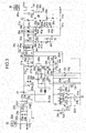
- Fig. 3 is a schematic diagram of the power supply apparatus 20 shown in Fig. 2 .
- the AC input section 22 includes a connector 22a through which the AC power is received from the AC switch section 21.
- the connector 22a is connected to power lines AC-L and AC-N and a ground line FG.
- a fuse 22b is inserted in the power line AC-L, and protects the primary side from excessive primary side current.
- the primary filter 23 is connected across the AC line AC-N and one of the terminals of the fuse 22.
- the primary filter 23 includes a capacitor 23c in parallel with a series circuit of resistors 23a and 23b, a choke coil 23d, a series circuit of capacitors 23e and 23f, and a capacitor 23g.
- the choke coil 23d includes a winding 23d1 connected between the resistor 23a and the capacitor 23e, and a winding 23d2 connected between the resistor 23b and the capacitor 23f.
- the junction of the capacitors 23e and 23f is connected to the ground line FG.
- the capacitor 23g is connected between the ground line FIG and the rectifier 24.
- the resistors 23a and 23b form a discharge path through which the capacitor 23c discharges its charge. The output of the primary filter 23 is fed to the rectifier 24.
- the rectifier 24 includes a diode for full-wave rectifying the AC power from the primary filter 23, and outputs the rectified AC power to the smoothing section 25.
- the smoothing section 25 includes a series of circuit of resistors 25b and 25c and an electrolytic capacitor 25a for smoothing the full-wave rectified AC power. The charge across the capacitor 25a is discharged through the series circuit of resistors 25b and 25c.
- a power thermistor 25d is inserted between the negative terminal of the capacitor 25a and another output terminal of the rectifier 24, and prevents rush current when the AC switch 21a is shifted to the ON position. The output of the smoothing section 25 is fed to the transformer 26.
- the shunt section 27 is connected across the start end pin 1 and finish end pin 3.
- the start end pin 1 is connected to the switching section 28.
- the shunt section 27 includes a series circuit of resistors 27a and 27b and a capacitor 27c in parallel with the series circuit of resistors 27a and 27b. This parallel circuit is in series with a shut diode 27d.
- the series circuit of the diode 27d and the parallel circuit is connected across the pin 1 and pin 3 of the primary winding 26a.
- the anode of the shunt diode 27d is connected to the start end P1 of the primary winding 26a.
- the switching section 28 includes the FET 28a, a parasitic capacitance 28b across the drain and cathode of the FET 28a, and a series circuit of a coil 28c and a resistor 28d.
- the FET 28a switches the current flowing through the primary winding 26a. When the FET 28a is turned off, a back electromotive force is developed across the primary winding 26a.
- the shunt section 27 shunts the back electromotive force.
- a resistor 29a constitutes a part of the current detecting section 29 and is connected between the smoothing section 25 and the source of the FET 28a, i.e., between the resistor 28d and the source of the FET 28a.
- the junction of the coil 28c and resistor 28d is connected to the control IC 30 via a parallel circuit of the resistor 28e and diode 28f.
- a diode 28g is connected to the junction of the resistor 28e and power thermistor 25d.
- the source of the FET 28a is connected to the IS terminal P3 of the control IC 30 via a series circuit of the resistors 29b and 29c.
- the start end pin 6 and finish end pin 5 of the auxiliary winding 26b of the transformer 26 are across the power supply terminal VCC P6 and ground terminal GND P4 of the control IC 30 via the rectifying/smoothing circuit 33.
- the rectifying/smoothing circuit 33 includes a diode 33a as a rectifier, a capacitor 33b in parallel with the diode 33a, a series circuit of a resistor 33c and a coil 33d connected to the cathode of the diode 33a, and an electrolytic capacitor 33e connected across the coil 33d and the finish end pin 5 of the auxiliary winding 26b.
- the output power of the auxiliary winding 26b is rectified by the diode 33a and is fed to the electrolytic capacitor 33e through the resistor 33c and coil 33d.
- the rectified power is smoothed by the electrolytic capacitor 33e before being supplied to the power supply terminal VCC P6 and ground terminal GND P4.
- the electrolytic capacitor 33e is in parallel with the Zener diode 33f and terminals 33h for an external capacitor.
- the negative electrode of the electrolytic capacitor 33e is connected to the negative electrode of the electrolytic capacitor 25a through a resistor 33g having a resistance of substantially zero ohms.
- the coil 33d is connected to the control IC 30 through a capacitor 33i.
- the resistor 29c is connected to the finish end pin 5 of the auxiliary winding 26b through a capacitor 33j.
- the control IC 30 is an element (e.g., available from Fuji Electric Semiconductors) that turns the FET 28a on and off.
- the control IC 30 includes a zero current detection signal input terminal (ZCD) P1, a feedback terminal (FB) P2, a current sense terminal (IS) P3, a ground terminal (GND) P4, an output terminal (OUT) P5, a power supply terminal (VCC) P6, a non-connected terminal (NC) P7, and a high voltage input terminal (VH) P8.
- ZCD zero current detection signal input terminal
- FB feedback terminal
- IS current sense terminal
- GND ground terminal
- OUT output terminal
- VCC power supply terminal
- NC non-connected terminal
- VH high voltage input terminal
- the ZCD terminal P1 is connected to the emitter of a photo transistor 32a of the primary alarm section 32.
- the photo transistor 32a receives the light emitted from a light emitting device 41f of the alarm signal receiving section 41.
- the photo transistor 32a and the light emitting device 41f constitute a photo-coupler.
- the ZCD terminal P1 is also connected to the junction of a resistor 32c and a capacitor 32d.
- the collector of the photo transistor 32a is connected to the start end pin 6 of the auxiliary winding 26b through the resistor 32b, coil 32d, resistor 33c, and the parallel circuit of the capacitor 33b and diode 33a. Another end of the resistor 33c is connected to the start end pin 6 of the auxiliary winding 26b.
- Another end of the capacitor 32d is connected to the finish end pin 5 of the auxiliary winding 26b.
- the photo transistor 32a is connected to the start end P to detect when the voltage at the start end pin 6 exceeds 7.2 V 2.3 ⁇ s after the FET 28a turns off, thereby protecting the regulator against overcurrent.
- a photo transistor 31a has its collector connected to the FB terminal P2 and its emitter connected to the finish end pin 5 of the auxiliary winding 26b.
- the photo transistor 31a and a later described light emitting device 40g constitute a photo-coupler.
- a capacitor 31b is connected across the collector and emitter of the photo transistor 31a.
- the IS terminal P3 is connected to the source of the FET 28a through the series circuit of the resistor 29c and 29b and is also connected to the finish end pin 5 of the auxiliary winding 26b through a capacitor 33j.
- the GND terminal P4 is connected to the finish end pin 5 of the auxiliary winding 26b and is also connected to the start end P6 of the auxiliary winding 26b through the capacitor 33i, coil 33d, resistor 33c and the parallel circuit of the capacitor 33b and diode 33a.
- the OUT terminal P5 is connected to the gate of the FET 28a through the resistor 28e and coil 28c.
- the VCC terminal P6 is connected to the start end pin 6 of the auxiliary winding 26b through the coil 33d, resistor 33c, and diode 33a.
- the VH terminal P8 is connected to the positive electrode of the electrolytic capacitor 25a through the resistor 25e.
- the control IC 30 performs the following functions.
- the control IC 30 switches the FET 28a from the latched state to the released state if the voltage on the VH terminal P8 decreases below a predetermined release threshold voltage below which the FET 28a is switched from the latched state to the released state.
- the control IC 30 compares the voltage on the FB terminal P2 connected to the photo transistor 31a with the voltage across the resistor 29a through which the current of the FET 28a flows, thereby adjusting the ON time during which the FET 28a is turned on.
- the secondary winding 26c of the transformer 26 has a start end pin 9 and a finish end pin 11.
- the finish end pin 11 is connected to one end of the resistor 33g through a capacitor 26d.
- the start end P9 is connected to the rectifying section 34.
- the rectifying section 34 rectifies the output power of the secondary winding 26c.
- the rectifying section 34 includes parallel diodes 34a and 34b, capacitors 34c and 34d in parallel with the diodes 34a and 34b.
- the smoothing section 35, bleeder resistor section 36, smoothing section 37, and DC power output section 38 are connected in cascade with the rectifying section 34.
- the smoothing section 35 smoothes out the current rectified by the rectifying section 34, and includes electrolytic capacitors 35a and 35b connected across the cathodes of the diodes 34a and 35b and the finish end pin 11 of the secondary winding 26c.
- the bleeder resistor section 36 includes resistors 36a, 36b, 36c, and 36d, and prevents the output voltage of the power supply apparatus 20 from decreasing when the load on the power supply apparatus 20 is not heavy.
- the smoothing section 37 smoothes out the output voltage of the power supply apparatus 20, and includes a coil 37a, an electrolytic capacitor 37b, and a capacitor 37c.
- the DC power output section 38 includes an output connector 38a through which the smoothed output voltage (e.g., 24 VDC) of the power supply apparatus 20 is outputted to the controller 50 shown in Fig. 2 .
- the electrode of 0 volts side of the output connector 38a is connected to the ground GND through a series circuit of capacitors 38b and 38c.
- the output of the smoothing section 37 is connected to the error voltage detecting section 39 and a secondary feedback section 40.
- the output of the rectifying section 34 is connected to the alarm signal receiving section 41.
- the error voltage detecting section 39 divides the DC output voltage of the smoothing section 37 to produce an error detection voltage, and sends the error detection voltage to the secondary feedback section 40.
- the error voltage detecting section 39 includes a resistor 39a, a variable resistor 39b, and the resistor 39c which are used to divide the voltage output.
- the series circuit of the resistor 39a, a variable resistor 39b, and the resistor 39c is connected across the electrolytic capacitor 37b.
- the secondary feedback section 40 includes a shunt regulator 40a, resistors 40b, 40c, and 40d, terminals 40e for connecting an external capacitor, a capacitor 40f, and a light emitting device 40g.
- the error voltage outputted from the error voltage detecting section 39 is fed to the reference electrode of the shunt regulator 40a.
- the shunt regulator 40a has its anode connected to the negative electrode of the electrolytic capacitor 37b, and its cathode connected to the cathode of the light emitting device 40g.
- the anode of the light emitting device 40g is connected to the input terminal of the coil 37a through the resistor 40b.
- the resistor 40d is in parallel with the light emitting device 40g.
- the terminals 40e for the external capacitor are connected between the cathode of the light emitting device 40g and reference terminal of shunt regulator 40a.
- a series circuit of the resistor 40c and capacitor 40f is connected across the reference electrode of the shunt regulator 40a and the cathode of the shunt regulator 40a.
- the resistor 39c is connected between the reference electrode and the anode of the shunt regulator 40a.
- the shunt regulator 40a When the voltage on the electrolytic capacitor 37b increases so that the voltage across the resistor 39c increases above a predetermined reference voltage set in the shunt regulator 40a, the shunt regulator 40a conducts through the anode and cathode electrodes. Thus, current flows through the light emitting device 40g, causing the light emitting device 40g to emit light. Conversely, if the output voltage on the electrolytic capacitor 37b decreases so that the voltage across the resistor 39c decreases below the predetermined reference voltage, the anode and cathode of the shunt regulator 40a do not conduct. Thus, the light emitting device 40g does not emit light.
- the alarm signal receiving section 41 includes a Zener diode 41a, resistors 41b, 41c, and 41d, diode 41e, and light emitting device 41f.
- the Zener diode 41a has its cathode connected to the positive electrode of the electrolytic capacitor 35a and its anode connected to the negative electrode of the electrolytic capacitor 37b via the resistor 41b and a parallel circuit of light emitting device 41f and the resistor 41c.
- the resistor 41c is connected across the anode and cathode of the light emitting device 41f.
- the alarm signal ALM-P indicates an abnormality that occurs in the controller 50, i.e., the load on the power supply apparatus 20, and is fed to the anode of the zener diode 41a through a series circuit of the resistor 41d and diode 41e.
- the light emitting device 41f emits light.
- the AC power is supplied through the AC switch section 21 to the AC input section 22.
- the input AC power passes through the primary filter 23, which removes noise from the AC power, to the rectifier 24.
- the input AC power is full-wave rectified by the rectifier 24, and is then smoothed by the smoothing section 25 into DC voltage.
- the smoothed DC voltage is switched on and off by the switching section 28 under the pulse width modulation (PWM) control of the control IC 30, and is supplied into the primary winding 26a of the transformer 26.
- PWM pulse width modulation
- the AC voltage across the secondary winding 26c is rectified by the rectifying section 34, and is then smoothed by the smoothing section 35 into DC voltage.
- the smoothed DC voltage is fed to the smoothing section 37 past the bleeder resistor section 36.
- the smoothing section 37 further smoothes the DC voltage and outputs the smoothed DC voltage to the DC power output section 38.
- the DC voltage outputted from the DC power output section 38 is then fed to the DC power input section 51 in the controller 50.
- the arithmetic operation/processing section of the controller 50 performs the arithmetic operation and signal processing, thereby producing control signals for driving the print engine 10 ( Fig. 1 ).
- the control signals are fed to the space motor driver 53 and print head driver 54.
- the driver space motor 53 drives the space motor 14 in the print engine 10 and the print head driver 54 drives the print head 11b, thereby printing on the sheet of print medium (not shown).
- the current flowing through the FET 28a is converted into a voltage across the resistor 29a.
- the voltage across the resistor 29c is applied to the IS terminal P3 of the controller IC 30 through the resistors 29b and 29c.
- the light emitting device 40g emits light.
- the photo transistor 31a turns on, causing the voltage on the FB terminal P2 of the control IC 30 to decrease.
- the photo transistor 31a operates in its linear region so that the voltage on FB terminal P2 is an analog voltage moving back and forth about a slice level of about 0.4 V.
- the photo transistor 31a operates as a switch so that the voltage on FB terminal P2 has a burst waveform having a repetition rate in a range of 0.3 to 120 kHz.
- the control IC 30 compares the voltage on the FB terminal P2 with the voltage on the IS terminal P3, and performs the PWM control based on the comparison results to output a switching signal having a variable duty from the OUT terminal P5 so that the ON time of the FET 28a becomes shorter.
- the switching signal is applied to the gate of the FET 28a through the resistor 28e and coil 28c, thereby setting a shorter ON time of the FET 28a. This decreases the DC voltage from the smoothing section 37.
- the light emitting device 40g does not emit light.
- the photo transistor 31a turns off, causing the voltage on the FB terminal P2 of the control IC 30 to increase.
- the control IC 30 outputs the switching signal, which sets a longer ON time of the FET 28a, from the OUT terminal P5. This increases the DC output voltage outputted from the smoothing section 37, thereby minimizing the fluctuation of the DC output voltage.
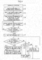
- Fig. 4 is a flowchart illustrating the operation for an alarm signal process shown in Figs. 2 and 3 .
- the controller 50 If the controller 50 is in an abnormal state, the controller 50 sends the alarm signal ALM-P to the power supply apparatus 20, thereby causing the FET 28a to stop its switching operation so that the power output of the power supply apparatus 20 is shut off (i.e., electric power is no longer supplied to the image forming apparatus). If the AC switch 21a remains in the ON position, the switching operation of the FET 28a remains latched. When the AC switch 21a is switched off, the switching operation of the FET 28a is maintained in the latched state at least for several minutes, until the voltage on the positive electrode of the electrolytic capacitor 25a decreases below the release threshold voltage. The AC switch 21a should then be shifted again to the ON position, thereby inputting the AC power again.
- the FET 28a is maintained in its latched state at least for several minutes even if the AC switch 21a is in the OFF state for the following reasons.
- the FET 28a is maintained in its latched state for several minutes in order for the user to recognize the occurrence of "malfunction" in the power supply apparatus 20.
- the FET 28a is switched to the latched state and the output power of the power supply apparatus 20 is no longer supplied to the image forming apparatus, most users may try to switch off and then back on again in a short time. If the image forming apparatus cannot be powered normally after repeating to switch on and off a few times, the users may usually believe that the power supply apparatus 20 has failed or malfunctioned. In this manner, the user is informed that the power supply apparatus 20 has failed.
- Fig. 5 shows the change in the charge remaining in the electrolytic capacitor 25a in terms of voltage on the electrolytic capacitor 25a after the AC switch 21a shown in Fig. 3 is shifted to the OFF position.
- Fig. 5 plots time in seconds as the abscissa and voltage in volts as the ordinate.
- Curve 60 represents the change in the voltage on the electrolytic capacitor 25a after the AC switch 21a is turned off and Curve 61 represents the change in the voltage on the electrolytic capacitor 25a when the FET 28a is normally switching.
- the capacitance of the electrolytic capacitor 25a is selected such that the output power of the power supply apparatus 20 can be provided reliably even if the change in the load on the power supply apparatus 20 fluctuates.
- the resistance values of the resistors 25b and 25c are selected to be large in order to minimize power consumption by the resistors 25b and 25c.
- the capacitance and resistances are as follows:
- the AC input voltage is 230 V
- the release threshold voltage is 30 V below which the FET 28a can be switched from the latched state to the released state.
- the voltage on the electrolytic capacitor 25a after the AC switch 21a is shifted to the OFF position follows curve 60.
- the FET 28a is switched from the latched state to the released state and the AC switch 21a becomes ready to switch on again.
- the Energy-related Products Directive requires that electronic apparatus have an auto-off function in which if an image forming apparatus is in an idle state longer than a certain period of time, the supply of power to the image forming apparatus is shut off.
- the auto-off function may be implemented as follows: The switching operation of the FET 28a is halted and the secondary side output power is shut off, for example, in response to the alarm signal ALM-P shown in Fig. 3 or by using a circuit that operates upon detection of an excessive voltage.
- One way of solving this drawback may be releasing the latched condition in a shorter time.
- a shorter releasing time is detrimental to the safe operation of the power supply apparatus.
- the alarm signal receiving section 41 shown in Fig. 3 is used for safe operation. Therefore, the time required for switching the FET 28a from the latched state to the released state after the AC switch 21a has been turned off cannot be merely shortened without good reasons.
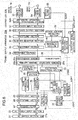
- Fig. 6 is a block diagram of a power supply apparatus 20A according to a first embodiment.
- the first embodiment differs from the comparative example in that the power supply apparatus 20A has a voltage supplying section 70 and a timer connecting section 71 on the primary side of the transformer 26, an alarm signal receiving section 72 on the secondary side of the transformer 26, and an auto-off signal receiving section 73 on the secondary side of the transformer 26.
- the auto-off signal receiving section 73 is used in place of the alarm signal receiving section 41 in the comparative example.
- a controller 50A includes an arithmetic operation/signal processing section 52A in place of the arithmetic operation/signal processing section 52.
- the voltage supplying section 70 is connected between the output of the primary filter 23 and the VH terminal P8 of the control IC 30, and applies the voltage on the capacitor of the primary side filter 23 to the VH terminal P8.
- the timer connecting section 71 is connected between the output of the smoothing section 25 and the VH terminal P3 of the control IC 30, and applies the voltage on the capacitor in the smoothing section 25 to the VH terminal P8 .
- the timer connecting section 71 operates in response to the light emitted from the alarm signal receiving section 72, thereby supplying the voltage on the capacitor 25a in the smoothing section 25 to the VH terminal of the control IC 30.
- the timer connecting section 71 and the alarm signal receiving section 72 constitute a power disconnecting section that prevents the power supply apparatus 20 from outputting its regulated DC output when the alarm signal ALM-P or the auto-off signal AUTO-OFF is received.
- the alarm signal receiving section 72 is connected to the output of the rectifying section 34, and monitors the output voltage of the rectifying section 34. If the alarm signal receiving section 72 detects an excess voltage higher than a predetermined value, the alarm signal receiving section 72 causes the timer connecting section 71 to operate. Alternatively, if the alarm signal ALM-P is received from a driver alarm detector 55, the alarm signal receiving section 72 emits light in response to the alarm signal ALM-P transmitted from the driver alarm detector 55 in the controller 50, thereby causing the timer connecting section 71 to operate.
- the auto-off signal receiving section 73 is connected to the output of the alarm signal receiving section 72 and emits light in response to an auto-off signal AUTO-OFF-2, thereby causing a primary alarm section 32 on the primary side of the transformer 26 to operate. Also, the auto-off signal receiving section 73 emits light in response to the light emission from the alarm signal receiving section 72, thereby causing the primary alarm section 32 to operate.
- the primary alarm section 32 and the auto-off signal receiving section 73 constitute an auto-off section when the auto-off signal AUTO OFF-P is received.
- the arithmetic operation/signal processing section 52A controls the respective sections in the controller 50, and includes a CPU and LSIs.
- the arithmetic operation/signal processing section 52A generates control signals for controlling the space motor driver 53, print head driver 54, and outputs the auto-off signal AUTO-OFF-P to the auto-off signal receiving section 73.
- the AUTO-OFF-P is a trigger signal for automatically turning off the power supply apparatus 20A if the image forming apparatus remains idle longer than a predetermined period of time.
- the AUTO-OFF-P is input to the power supply apparatus 20A, the output power of the power supply apparatus 20 is shut off.
- the AUTO-OFF-P allows the AC power to be supplied promptly to the power supply apparatus when the AC switch 21a is switched on again after having been switched off due to malfunction.
- the other portions of the configuration are the same as those of the comparative example.
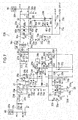
- Fig. 7 is a schematic diagram illustrating the configuration of the power supply apparatus 20A. Elements similar to those of the comparative example have been the same reference characters and their description is omitted.
- the voltage supplying section 70 rectifies the AC voltage on the AC-L line at the output of the primary filter 23, and supplies the rectified voltage to the VH terminal P8 of the control IC 30.
- the voltage supplying section 70 includes a diode 70a, resistor 70b, a plurality of Zener diodes 70c, 70d, and 70e, which form a series circuit connected between the electrode of the capacitor 23e and the VH terminal P8.
- each Zener diode has a zener voltage of about 27 V.
- the resistor 33g, power thermistor 25d, and one of four diodes in the rectifier 24 make a return path for the current rectified by the diode 70a.
- the control IC 30 as a controller and the FET 28a as a switching element constitute a switching section that switches the current flowing through the primary winding 26a.
- the capacitor 33e is charged by the voltage obtained by half-wave rectifying the output of the auxiliary winding 26b.
- the control IC 30 operates on the voltage applied to the VH terminal of the control IC 30 or the voltage applied to the VCC terminal of the control IC 30.
- the VH terminal and VCC terminal are connected through an internal circuit.
- the timer connecting section 71 operates in response to the light emitted by the alarm signal receiving section 72 and supplies the voltage on the electrolytic capacitor 25a in the smoothing section 25.
- the timer connecting section 71 includes a resistor 71a, a capacitor 71b, a diode 71c, resistors 71d, 71e, and 71f, and a phototriac 71g.
- the phototriac 71g turns on in response to the light emitted from the alarm signal receiving section 72.
- the phototriac 71g has its anode connected to the positive electrode of the electrolytic capacitor 25a of the smoothing section 25 and its cathode connected to the VH terminal P8 of the control IC 30 through a parallel circuit of the resistor 71a and capacitor 71b, the diode 71c, and the resistor 71d.
- the cathode of the phototriac 71g is connected to the negative electrode of the electrolytic capacitor 25a through a parallel circuit of the resistor 71a and capacitor 71b and a series circuit of the resistors 71e and 71f.
- the alarm signal receiving section 72 includes a Zener diode 72a, resistors 72b and 72c, a diode 72d, and a light emitting device 72e.
- the light emitting device 72e and the phototriac 71g constitute a phototriac coupler.
- the alarm signal ALM-P is applied to the anode of the light emitting device 72e through the resistor 72c, diode 72d and resistor 72b.
- the junction of the diode 72d and resistor 72b is connected to the positive electrode of the rectifying section 34 through a Zener diode 72a.
- the light emitting device 72e which is a part of the phototriac coupler, emits when voltage is applied thereto, thereby causing the phototriac 71g, which is a part of the phototriac coupler, to turn on.
- the phototriac coupler once the phototriac 71g turns on, it remains turned on even if the light emitting device 72e stops emitting light.
- the auto-off signal receiving section 73 includes resistors 73a and 73b, a diode 73c, and a light emitting device 73d.
- the light emitting device 73d and photo transistor 32a constitute a photo coupler.
- the auto-off signal AUTO-OFF-P is inputted through the resistor 73b and diode 73c to the anode of the light emitting device 73d.
- the anode of the light emitting device 73d is connected to the cathode of the light emitting device 72e.
- the resistor 73a is connected between the anode and cathode of the light emitting device 73d.
- the light emitting device 73d emits light upon application of voltage, thereby causing a photo transistor 32a to turn on.
- the other portions of the configuration are the same as those of the comparative example shown in Fig. 3 .
- the light emitting device 73d emits light, causing the photo transistor 32a to turn on so that the voltage on the ZCD terminal is higher than the latch threshold voltage of the latch circuit set in the control IC 30.
- the control IC 30 stops outputting a switching signal from the OUT terminal P5 to the FET 28a, causing the FET 28a to stop switching on and off so that the DC supply voltage on the VCC terminal of the control IC 30 is lost.
- the power supply apparatus 20A enters an auto-off state.
- the voltage is still applied to the VH terminal P8 through the diode 70a, resistor 70b, Zener diodes 70c, 70d and 70e.
- the voltage applied to the VH terminal P8 is also applied to the VCC terminal P6 via an internal circuit in the control IC 30, thus enabling the control IC 30 to normally operate.
- the latch circuit remains latched even if the auto-off signal (AUTO-OFF-P) disappears, until the voltage on the VH terminal P8 decreases below the release threshold voltage of the latch circuit set in the control IC 30. In order to release the latch circuit from the latched state, the voltage on the VH terminal P8 must be decreased below the release threshold voltage.
- the voltage is no longer applied to the VH terminal through the diode 70a, resistor 70b, and Zener diodes 7Oc, 70d, and 70e, so that the voltage on the VH terminal IC 30 decreases to zero volts. If the user then turns on the Ac switch 21a again, the power supply apparatus 20A will return from the auto-off state to the normal operating state.
- the light emitting device 72e emits light, causing the phototriac 71g to turn on, and the light emitting device 73d emits light, causing the photo transistor 32a to turn on. Since the phototriac 71g has turned on, the voltage on the capacitor 25a is applied to the VH terminal of the control IC 30. The voltage rectified by the diode 70a is also applied to the VH terminal of the control IC 30 through the resistor 70b and Zener diodes 70c, 70d, and 70e. The voltage on the VH terminal P8 is fed to the VCC terminal P6 via the internal circuit in the control IC 30, so that the control IC 30 normally operates.
- the photo transistor 32a Since the photo transistor 32a has turned on, the voltage on the ZCD terminal exceeds the latch threshold voltage to trigger the latch circuit in the control IC 30 and triggers the latch circuit.
- the latch circuit holds the latched state even if the alarm signal (ALM-P) disappears.
- the latched state lasts until the voltage on the VH terminal P8 decreases below the release threshold voltage set in the control IC 30.
- the voltage rectified by the diode 70a and applied to the VH terminal P8 via the diode 70a, resistor 70b, and Zener diodes 70c, 70d, and 70e will decrease quickly.
- the voltage on the capacitor 25a will then gradually decrease mainly through the resistors 25b and 25c in accordance with the time constant given by the capacitor 25a and resistors 25b and 25c.
- the latch circuit is released from the latched state. If the user then turns on the AC switch 21a again, the power supply apparatus 20A will return from the alarm state to the normal operating state.
- Fig. 8 is a flowchart illustrating the overall operation of the power supply apparatus 20A shown in Fig. 6 and Fig. 7 .
- the power supply apparatus 20A begins to operate.
- the power supply apparatus 20A waits for the auto-off signal AUTO-OFF-P or the alarm signal ALM-P from the controller 50A. Just as in the comparative example, the power supply apparatus 20A receives the AC power through the AC switching section 21 and AC input section 22, and outputs regulated stable DC power from the DC power output section 38.
- the space motor driver 53 drives the space motor 14 ( Fig. 1 ) and the print head driver 54 drives the print head 11b ( Fig. 1 ), thereby printing on the sheet of print medium.
- Fig. 9 is a block diagram of the power supply apparatus 20A, illustrating the auto-off signal process in S23 shown in Fig. 8 .
- Fig. 9 corresponds to Fig. 6 .
- the solid line in Fig. 9 shows the flow of signals when the auto-off signal AUTO-OFF-P is generated in the controller 50A and the power supply apparatus 20A is shut off automatically accordingly.
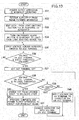
- Fig. 10 is a flowchart illustrating the operation of the auto-off signal process when the auto-off signal AUTO-OFF-P is received and the power supply apparatus 20A is shut off automatically accordingly.
- S31 The power supply apparatus 20A is normally operating.
- the control IC 30 compares the voltage on the ZCD terminal with the latch threshold voltage. If the voltage on the ZCD terminal ⁇ the latch threshold voltage (YES at S36), the program proceeds to S37.
- the latch threshold voltage may be, for example, 7.2 V, and if the voltage on the ZCD terminal remains equal to or higher than 7.2 V for at least 57 ⁇ s, it may be determined that the voltage on the ZCD terminal ⁇ the latch threshold voltage.
- the control IC 30 sets the OUT terminal P5 to the off state, thereby switching the FET 28a to the latched state where the FET 28a remains turned off. In the latched state, the capacitor 33e is no longer charged by the DC voltage obtained by rectifying the voltage across the auxiliary winding 26c. If the voltage on the ZCD terminal ⁇ the latch threshold voltage (NO at S36), the program jumps back to S35 where the control IC 30 allows the FET 28a to continue its switching operation until the voltage on the ZCD terminal increases so that the voltage on the ZCD terminal ⁇ the latch threshold voltage.
- the control IC 30 compares the voltage on the VCC terminal P6 with the reference voltage set in the control IC 30. If the voltage on the VCC terminal > the release threshold voltage (e.g.; 7 V) (NO at S38), the program proceeds to S39.
- the release threshold voltage e.g. 7 V
- the output of the choke coil 23d is half-wave rectified the diode 70a and is then applied to the VH terminal P8 through a series circuit of the resistor 70b and Zener diodes 70c, 70d, and 70e.
- the voltage on the VH terminal P9 of the control IC 30 is the difference between the voltage half-wave rectified by the diode 73a and the voltage across the Zener diodes 70c, 70d, and 70e. Therefore, the voltage on the VH terminal P8 continues to charge the capacitor 33e, so that the voltage on the VCC terminal of the control IC 30 will not decrease below the reference voltage below which the FET 28a is switched from the latched state to the released state.
- the program jumps back to S38 and the FET 28a remains in the latched state until the AC switch 21a is shifted to the OFF position.
- Fig. 11 is a block diagram illustrating the operation at S24 ( Fig. 8 ) where the alarm signal is processed. Fig. 11 corresponds to Fig. 6 .
- the solid line in Fig. 11 shows the flow of signals when the auto-off signal AUTO-OFF-P is generated and the power supply apparatus 20A is therefore shut off automatically.
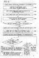
- Fig. 12 is a flowchart illustrating the operation at S24 ( Fig. 8 ) where the alarm signal process is performed.
- the flowchart illustrates the operation for shutting off the power supply apparatus 20A in response to the alarm signal ALM-P.
- S56 The control IC 30 compares the voltage on the ZCD terminal with the latch threshold voltage. If the voltage on the ZCD terminal ⁇ the latch threshold voltage (NO at S56), the program jumps back to S55 and the control IC 30 will allow the FET 28a to continue its switching operation until the voltage on the ZCD terminal increases. If the voltage on the ZCD terminal ⁇ the latch threshold voltage (YES at S56), the program proceeds to S57.
- the VH terminal P8 receives the voltage half-wave rectified by the diode 70a and the voltage supplied from the capacitor 25a, the voltages charging the electrolytic capacitor 33e. The program then proceeds to S60.
- S60 The control IC 30 compares the voltage on the VH terminal with the release threshold voltage. If the voltage on the VH terminal > the release threshold voltage (NO at S60), the program proceeds to S61.
- the process at S54, S55, S56, and S57 may be performed concurrently with the process at S58.
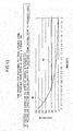
- Fig. 13 illustrates the charge remaining in the capacitor 23c after the AC switch 21a ( Fig. 7 ) is switched off.
- Fig. 13 plots time as the abscissa and voltage as the ordinate.
- Curve 80 shows the voltage on the capacitor 23c after the Ac switch 21a is switched off.
- Curve 81 shows the voltage on the capacitor 23c when the FET 28a is switched from the latched state to the released state. The charge remaining in the capacitor 23c after the AC switch 21a is switched off will be described with reference to Fig. 13 .
- the capacitor 23c and resistors 23c and 23b through which the voltage on the capacitor 23c is discharged must meet requirements in the immunity rest and the residual charge decay time requirements of IEC 60950 safety standards. For this reason, the capacitance of the capacitor 23c and the resistance of the resistors 23a and 23b are selected to meet the discharge time requirements and noise filtering requirement.
- the voltage on the VH terminal P9 of the control IC 30 is the difference between the voltage half-wave rectified by the diode 73a and the voltage across the Zener diodes 70c, 70d, and 70e. Assume that capacitor 23c and resistors 23a and 23b have the following values. Capacitor 23c: 0.47 ⁇ F Resistor 23a: 470 k ⁇ Resistor 23b: 470 k ⁇
- the AC input voltage is 230 V
- the release threshold voltage is 30 V.
- the voltage on the capacitor 23c follows Curve 80 after the AC switch 21a has been switched off.
- the voltage on the capacitor 25a is 111 V 0. 47 seconds after the AC switch 21a is switched off, the FET 28a is switched from the latched state to the released state so that the AC switch 21a can be switched on again.
- the voltage on the electrolytic capacitor 25a in the smoothing section 25 after the AC switch 21a is switched off follows Curve 60 ( Fig. 5 ), assuming that the AC input voltage is 230 V and the release threshold voltage in the control IC 30 below which the FET 28a is switched from the latched state to the released state is 30 V.
- the voltage on the electrolytic capacitor 25a has decreased to 30 V, i.e., about 157 seconds after the AC switch 21a is switched off the FET 28a is switched from the latched state to the released state so that the AC switch 21a can be switched on again after the AC switch 21a is switched off.
- the voltage on the capacitor 23c promptly decreases to the release threshold voltage in about 0. 47 seconds, so the AC switch 21a can be switched on again promptly after the AC switch 21a is switched off.
- the voltage on the electrolytic capacitor 25a decreases to the release threshold voltage about 157 seconds after the AC switch 21a is switched off. In other words, the user has to wait for about 157 seconds before the AC switch 21a can be switched on again after the AC switch 21a is switched off.
- the auto-off signal AUTO-OFF-P is used for automatically turning off the power supply of the image forming apparatus.
- the alarm signal ALM-P indicates the occurrence of an abnormality in the image forming apparatus. If the AUTO-OFF-P is received, the voltage on the capacitor 25c in the primary filter 23 of the power supply apparatus 20A is used to enable the prompt power-up after the AC switch 21a is switched off.
- the light emitting device 72e and the phototriac 71g operate so that the voltage on the capacitor 25a is used which has been charged by the full-wave rectified AC power by the rectifier 24 and smoothed by the smoothing section 25.
- a waiting time of several minutes can be ensured for safe operation of the power supply apparatus 20A before the AC switch 21a can be switched on again after the AC switch 21a is switched off.
- Fig. 14 is a block diagram of a power supply apparatus 20B according to a second embodiment. Elements similar to those of the comparative example shown in Fig. 2 have been given the same reference numerals, and their description is omitted.
- the power supply apparatus 20B differs from the power supply apparatus 20A in that a relay driver 90 and a B-contact relay 91 are used and an alarm signal receiving section 41 and an auto-off signal receiving section 92 are employed.
- the relay driver 90 is connected to the output of the rectifier 24 and operates in response to the light emitted from the auto-off signal receiving section 92, thereby causing the B-contact relay 91.
- the B-contact relay 91 electrically connects or disconnects the rectifier 24 from smoothing section 25.
- the B-contact relay 91 is normally ON to connect between the smoothing circuit 24 and rectifier 25. Once the relay driver 90 operates, the B-contact relay 91 becomes off to electrically disconnect the rectifier 24 and smoothing section 25.
- the auto-off signal receiving section 92 operates to emit light in response to the auto-off signal AUTO-OFF-P transmitted from the arithmetic operation/signal processing section 52A, thereby causing the relay driver 90 on the primary side of the transformer 26.
- the primary alarm section 32 and the alarm signal receiving section section 41 constitute a power disconnecting section.
- the relay driver 90 and B-contact relay 91 on the primary side of the transformer 26 and the auto-off signal receiving section 92 constitute an auto-off section.
- the other portions of the configuration are the same as those of the comparative example shown in Fig. 2 and the first embodiment.
- Fig. 15 is a schematic diagram illustrating the configuration of the power supply apparatus 20B shown in Fig. 14 .
- the relay driver 90 includes a phototriac 90a, resistors 90b and 90e, an energizing coil 90c, a capacitor 90d, and a Zener diode 90f.
- the phototriac 90a receives the light emitted by a light emitting device 92b.
- the light emitting device 92b and the phototriac 90a constitute a phototriac coupler.
- a light emitting device 40g and a photo transistor 31a constitute a photo coupler.
- the phototriac 90a has its anode connected to the output of the rectifier 24 and its cathode connected to the negative electrode of the electrolytic capacitor 25a of the smoothing section 25 through the resistor 90b and energizing coil 90c.
- the cathode of the phototriac 90a is connected to a parallel circuit of the capacitor 90d and resistor 90e.
- the energizing coil 90c is used to drive the B-contact relay 91.
- the energizing 90c is connected in parallel with a Zener diode 90f.
- the Zener diode 90f shunts the back electromotive force developed across the energizing coil 90c.
- the B-contact relay 91 is connected between the output of the rectifier 24 and the smoothing section 25. When no current flows through the energizing coil 90c and therefore the energizing coil 90c is not energized, the relay contacts are closed. When current flows through the energizing coil 90c and therefore the energizing coil is energized, the relay contacts are open.
- the auto-off signal receiving section 92 includes a resistor 92a through which the auto-off signal AUTO-OFF-P is inputted and the light emitting device 92b of the phototriac coupler.
- the light emitting device 92b is connected between the ground part of the resistor 92a and a light emitting device 41f in the alarm signal receiving section 41.
- the light emitting device 41f and a later described photo transistor 32a constitute a photo coupler.
- the light emitting device 41f emits light, causing the phototriac 90a to turn on.
- the phototriac couplers behave as follows: Once the phototriac 90a is turned on, the phototriac 90a continues to be turned on, even if the light emitting device 92b stops emitting light.
- the other part of the configuration is the same as those of the comparative example shown in Fig. 3 and the first embodiment shown in Fig. 6 .
- the light emitting device 92b emits light, causing the phototriac 90a to turn on so that current flows through the energizing coil 90c to make the contacts of the relay 91 open.
- the relay 91 has a short delay time for the contacts to open. In other words, the contacts will not open for a short time immediately after the phototriac 90a turns on.
- the phototriac 90a remains turned on as long as the rectifier 24 supplies the power supply voltage to the phototriac 90a.
- the capacitor 25a discharges during the delay time through the closed contacts, phototriac 90a, resistor 90b, and energizing coil 90c.
- the voltage on the capacitor 25a applied to the VH terminal becomes lower than a reference voltage preset in the control IC 30.
- the contacts of the relay 91 open. Once the contacts of the relay 91 become open, the succeeding stage of the relay 91 loses its power supply voltage and the FET 28a stops its switching operation. The voltage across the auxiliary winding 26b also becomes zero. In this manner, the power supply apparatus 20A enters an auto-off state.
- the phototriac 90a shown in Fig. 15 remains turned on even if the auto-off signal (AUTO-OFF-P) disappears.
- the user In order to bring the power supply apparatus 20B out of the auto-off state, the user must to bring the AC switch 21a to the off position, thereby turning off the phototriac 90a.
- the phototriac 90a turns off so that the contacts of the relay 91 are again closed.
- the voltage of the capacitor 25a applied to the VH terminal will increase, so that the power supply apparatus 20A will return from the auto-off state to the normal operating state.
- the light emitting device 41f emits light, causing the photo transistor 32a to turn on.
- the voltage rectified by the rectifier 24 remains applied to the VH terminal of the control IC 30 through the resistor 25e.
- the voltage on the VH terminal P8 is fed to the VCC terminal P6 via the internal circuit in the control IC 30, so that the control IC 30 normally operates.
- the photo transistor 32a Since the photo transistor 32a has turned on, the voltage on the ZCD terminal exceeds the latch threshold voltage to trigger the latch circuit in the control IC 30 and triggers the latch circuit.
- the latch circuit holds the latched state even if the alarm signal (ALM-P) disappears.
- the latched state lasts until the voltage on the VH terminal P8 decreases below the release threshold voltage set in the control IC 30.
- the voltage on the capacitor 25a will gradually decrease mainly through the resistors 25b and 25c in accordance with the time constant given by the capacitor 25a and resistors 25b and 25c.
- the latch circuit is released from the latched state so that the control IC becomes ready to drive the FET 28a to switch on and off again. If the user then turns back on the AC switch 21a again, the power supply apparatus 20B will return from the alarm state to the normal operating state.
- Fig. 16 is a flowchart illustrating the overall operation of the power supply apparatus 20B shown in Fig. 14 and Fig. 15 .
- the power supply apparatus 20B begins to operate.
- the power supply apparatus 20B waits for the auto-off signal AUTO-OFF-P or the alarm signal ALM-P. Just as in the power supply apparatus 20A of the first embodiment, the power supply apparatus 20B receives the AC power through the AC switch 21a and AC input section 22, and outputs regulated stable DC power from the DC power output section 38.
- the space motor driver 53 drives the space motor 14 ( Fig. 1 ) and the print head driver 54 drives the print head 11b ( Fig. 1 ), thereby printing on a sheet of print medium.
- the program Upon reception of the auto-off signal AUTO-OFF-P from the arithmetic operation/signal processing section 52A of the controller 50A, the program proceeds to S72 where an auto-off signal process is performed and then the program ends. Alternatively, upon reception of the alarm signal ALM-P outputted from the driver alarm detector 55 of the controller 50A, the program proceeds to S73 where an alarm signal process is performed and then the program ends.
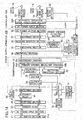
- Fig. 17 is a block diagram illustrating the power supply apparatus 20B, illustrating the auto-off signal process in S73 ( Fig. 16 ). Fig. 17 corresponds to Fig. 14 .
- Fig. 17 shows the flow of signals when the auto-off signal AUTO-OFF-P is generated and the power supply apparatus 20B is shut off automatically.
- Fig. 18 is a flowchart illustrating the auto-off signal process. The flowchart shown in Fig. 18 will be described with reference to Figs. 15 and 17 .
- the other operations e.g., when the alarm signal ALM-P is received, are the same as that of the first embodiment.
- the auto-off signal AUTO-OFF-P is used for automatically turning off the power supply of the image forming apparatus 20B.
- the alarm signal ALM-P indicates the occurrence of an abnormality in the image forming apparatus which is the load on the power supply apparatus 20B. If the AUTO-OFF-P is received, the contacts of the B-relay 91 are made open and the rel ay driver 90 maintains the contacts open, thereby preventing the electric power rectified by the rectifier 24 from being supplied to the smoothing section 25. This leaves the output power on the secondary side of the transformer 26 effectively disconnected, allowing the power supply apparatus 20B to be turned on again promptly after the AC switch 21a is switched off. In other words, the latching function of the control IC 30 remains inactive, allowing the power supply apparatus 20B to be turned on again immediately after the auto-off process.
- the present invention is not limited to the first and second embodiments and a variety of modifications may be made.
- the configuration of the power supply apparatus 20A and 20B may be changed.
- the print engine may be of the other configuration.
- the image forming apparatus used in the present invention may be other types of printers such as copying machine, facsimile machine, and multi function peripheral (MFP).
- printers such as copying machine, facsimile machine, and multi function peripheral (MFP).
- a power supply apparatus (20A, 20B) supplies regulated power to an external apparatus (50A).
- a power switch (21a) is turned on to receive AC power and turned off not to receive the AC power.
- the AC power is rectified by a rectifying section (24) and is switched by a switching section (30, 28, 26) into switched DC power which is smoothed by a rectifying/smoothing section (34, 35) .
- the power disconnecting section 25a, 25b, 25c, 71, 72
- the power disconnecting section allows receiving of the AC power only a time (25a, 25b, 25c) after turn-off of the power switch.
- an auto-off section Upon reception of an auto-off signal indicative of an idle state of the external apparatus, an auto-off section does not send the switched DC power to the rectifying/smoothing section.
Landscapes
- Physics & Mathematics (AREA)
- General Physics & Mathematics (AREA)
- Engineering & Computer Science (AREA)
- Microelectronics & Electronic Packaging (AREA)
- Dc-Dc Converters (AREA)
- Accessory Devices And Overall Control Thereof (AREA)
- Control Or Security For Electrophotography (AREA)
- Direct Current Feeding And Distribution (AREA)
Abstract
Description
- The present Invention relates to a switching mode power supply apparatus and an image forming apparatus that incorporates the switching mode power supply apparatus.
- A conventional image forming apparatus incorporates a power supply apparatus and a printer apparatus that operates on the power supply apparatus. The power supply apparatus is configured to receive an AC power through a main switch and convert the AC power into DC power. When an abnormality occurs in the printer apparatus, the printer apparatus sends an alarm signal to the power supply apparatus.
- Japanese Patent Publication No. H10-27072 discloses a technology in which when an abnormality occurs in the load of a power supply apparatus, the power supply apparatus is switched off.
- Such a conventional image forming apparatus has an AUTO OFF function in which if the printer apparatus is idle for more than a predetermined period of time, the power supply apparatus is automatically switched off. This type of image forming apparatus suffers from the following drawbacks.
- Upon occurrence of an abnormality, the printer apparatus sends an alarm signal to the power supply apparatus, which in turn is automatically switched off. The power switch is then shifted to "OFF." When the power switch is again shifted to "ON, " the AC power is not supplied until a certain period of time elapses before the power supply apparatus is released from the latched state. This is true for an auto-off function if the auto-off function is added to the power supply apparatus. This is inconvenient.
- One way of solving this drawback may be releasing the pwer supply apparatus from the latched state in a shorter time. However, a shorter releasing time is detrimental to safe operation of the power supply apparatus. Accordingly, a need exists in the art for a solution to the aforementioned drawbacks.
- The present invention was made to solve the aforementioned drawbacks.
- An object of the invention is to provide a power supply apparatus in which an auto-off signal is received from an external apparatus, the output power is shut off but becomes ready to be switched on again after auto-off process has been performed.
- An object of the invention is to provide a power supply apparatus in which an alarm signal is received from an external apparatus, the output power is shut off but becomes ready to be switched on again only after a predetermined period of time has passed.
- A power supply apparatus (20A, 20B) supplies regulated power to an external apparatus (50A). A power switch (21a) is turned on by a user to receive AC power and is turned off by the user not to receive the AC power. A rectifying section (24) rectifies the AC power to produce DC power. A switching section (30, 28, 26) switches the DC power to produce switched DC power. A rectifying and smoothing section (34, 35) smoothes the switched DC power. A power disconnecting section (25a, 25b, 25c, 71, 72) stop sending the switched DC power to the smoothing section (34, 35) if the power disconnecting section receives an alarm signal (ALM-P) indicative of occurrence of an abnormality in the external apparatus (50A). If the AC switch is turned off and then turned back on again by the user after stops sending the switched DC power to the smoothing section (34, 35) in response to the alarm signal (ALM-P), the power disconnecting section allows the power supply apparatus to receive the AC power only a period of time (25a, 25b, 25c) after power switch is turned off. An auto-off section stops sending the switched DC power to the succeeding stage if the auto-of section receives an auto-off signal (AUTO-OFF-P) indicative that the external apparatus is in an idle mode.
- Further scope of applicability of the present invention will become apparent from the detailed description given hereinafter. However, it should be understood that the detailed description and specific examples, while indicating preferred embodiments of the invention, are given by way of illustration only, since various changes and modifications within the spirit and scope of the invention will become apparent to those skilled in the art from this detailed description.
- The present invention will become more fully understood from the detailed description given hereinbelow and the accompanying drawings which are given by way of illustration only, and thus are not limiting the present invention, and wherein:
-
Fig. 1 is a perspective view illustrating the general configuration of a print engine according to the invention; -
Fig. 2 is a block diagram illustrating a power supply apparatus as a comparative example; -
Fig. 3 is a schematic diagram of the power supply apparatus shown inFig. 2 ; -
Fig. 4 is a flowchart illustrating the operation of the comparative example in the alarm signals process; -
Fig. 5 shows the change in the charge remaining in the electrolytic capacitor in terms of voltage on the electrolytic capacitor after the AC switch shown inFig. 3 is shifted to the OFF position; -
Fig. 6 is a block diagram of apower supply apparatus 20A according to a first embodiment. -
Fig. 7 is a schematic diagram illustrating the configuration of the power supply apparatus according to a first embodiment; -
Fig. 8 is a flowchart illustrating the overall operation of the power supply apparatus shown inFig. 6 andFig. 7 ; -
Fig. 9 is a block diagram of the power supply apparatus, illustrating the auto-off signal process; -
Fig. 10 is a flowchart illustrating the operation of the auto-off signal process when the auto-off signal is received and the power supply apparatus according to the first embodiment is shut off automatically; -
Fig. 11 is a block diagram illustrating the operation at S24 shown inFig. 8 where the alarm signal is processed; -
Fig. 12 is a flowchart illustrating the operation at S24 shown inFig. 8 where the alarm signal is processed; -
Fig. 13 illustrates the charge remaining in the capacitor after the AC switch is switched off; -
Fig. 14 is a block diagram of a power supply apparatus 20B according to a second embodiment; -
Fig. 15 is a schematic diagram illustrating the configuration of the power supply apparatus shown inFig. 14 ; -
Fig. 16 is a flowchart illustrating the overall operation of the power supply apparatus shown inFig. 14 andFig. 15 ; -
Fig. 17 is a block diagram illustrating the power supply apparatus shown inFig. 14 , illustrating the auto-off signal process in S73 shown inFig. 16 ; and -
Fig. 18 is a flowchart illustrating the auto-off signal process. - The present invention will be described by way of embodiments. Various structures, systems and devices are schematically depicted in the drawings for purposes of explanation only and are not to limit the present invention to preferred embodiments.
- An image forming apparatus according to a first embodiment incorporates a flyback switching mode power supply apparatus and a printer that operates on DC power supplied from the flyback switching mode power supply apparatus.
-
Fig. 1 is a perspective view illustrating the general configuration of aprint engine 10. Theprint engine 10 is a pertinent portion of a dot-impact serial printer, and includes acarriage unit 11. Thecarriage unit 11 incorporates aprint head 11b used for printing on a sheet of print medium, e.g., paper. Thecarriage unit 11 is fixed to abelt 12 that is disposed horizontally about apulley 13 and agear 14a mounted on aspace motor 14. Thebelt 12 has teeth in meshing engagement with thegear 14a and thepulley 13. Thepulley 13 is free to rotate. When thespace motor 14 is energized to rotate, thebelt 12 is driven to run by thegear 14a so that thecarriage unit 11 runs back and forth in the horizontal direction. - The
print head 11b andspace motor 14 are driven by drivers (not shown) in accordance with commands from a controller (not shown). Theprint head 11b operates in accordance with a print command to strike an ink ribbon (not shown) impregnated with ink, thereby printing on the sheet of print medium (not shown). Theprint engine 10 is capable of simultaneously printing on multiple sheets of paper. -
Fig. 2 is a block diagram illustrating apower supply apparatus 20 as a comparative example. - The
power supply apparatus 20 supplies DC power to acontroller 50 that controls the operation of thespace motor 14 andprint head 11b of theprint engine 10. Thepower supply apparatus 20 is built on, for example, a power supply circuit board (not shown). - The
power supply apparatus 20 includes anAC switch section 21 with which an ACpower input section 22, aprimary filter 23 on the primary side of atransformer 26, arectifier 24, and a smoothingsection 25 are connected in cascade in this order. - The
AC switch section 21 includes anAC switch 21a as a power switch, which is operated by the user to receive AC power or disconnect the AC power. TheAC switch section 21 is connected to theAC input section 22 through a connector. TheAC input section 22 includes the connector connected to theprimary filter 23. Theprimary filter 23 removes noise on the primary side of thetransformer 26. Therectifier 24 is a diode bridge which is an arrangement of four diodes in a bridge circuit configuration, and full-wave rectifies the AC power, inputted through theprimary filter 23, into DC power. The smoothingsection 25 smoothes the rectified DC power, and feeds the smoothed DC power to thetransformer 26. - The
transformer 26 is a flyback transformer that includes a primary winding 26a, an auxiliary winding 26b, a secondary winding 26c. The primary winding 26a is connected to ashunting section 27, aswitching section 28, acurrent detector 29, and acontrol IC 30. Thecontrol IC 30 is designed to control the switching operation of the switching regulator. The auxiliary winding 26b is used for supplying electric power to thecontrol IC 30 and is connected to thecontrol IC 30 through a rectifying/smoothingsection 33. Thecontrol IC 30 is connected to aprimary feedback section 31 and aprimary alarm section 32 on the primary side of thetransformer 26. A rectifyingsection 34, a smoothingsection 35, ableeder resistor section 36, a smoothingsection 37, a DCpower output section 38, an errorvoltage detecting section 39, asecondary feedback section 40 on the secondary side of thetransformer 26, and an alarmsignal receiving section 41 on the secondary side of thetransformer 26 are connected in cascade in this order to the secondary winding 26c of thetransformer 26. - The
shunt section 27 is connected in parallel with the primary winding 26a. When theswitching section 28 is switched off, theshunt section 27 forms a shunt path that shunts the back electromotive force developed across the primary winding 26a. The switchingsection 28 includes switching elements formed of, e.g., field effect transistor (FET) 28a (Fig. 3 ) that switches the current through the primary winding 26a. The current detectingsection 29 is connected to theFET 28a in theswitching section 28. Thecurrent detector 29 converts the detected current value into a corresponding voltage value, and the output of thecurrent detector 29 is connected to thecontrol IC 30. The rectifying/smoothingcircuit 33 rectifies the output voltage of the auxiliary winding 26b into direct current, and smoothes the rectified direct current before the direct current is fed to thecontrol IC 30. - The
primary feedback section 31 operates in cooperation with thesecondary feedback section 40. Theprimary alarm section 32 operates in cooperation with the alarmsignal receiving section 41 on the secondary side of thetransformer 26. The output of theprimary alarm section 32 is fed to thecontrol IC 30. - The
control IC 30 compares the output voltage of theprimary feedback section 31 with the output voltage of thecurrent detector 29 to control the ON/OFF time of theswitching section 28. Thecontrol IC 30 monitors the output voltage of theprimary alarm section 32, so that when the output voltage exceeds a predetermined value which has been set in thecontrol IC 30 in advance, thecontrol IC 30 forcibly causes the switching operation of theswitching section 28 to halt and to remain halted unless the output voltage of the smoothingsection 25 decreases below the predetermined value. - The rectifying
section 34 is connected to the secondary winding 26c, and rectifies the output power of the secondary winding 26c. The output of the rectifyingsection 34 is connected to the smoothingsection 35 and alarmsignal receiving section 41. The smoothingsection 35 smoothes out the output of the rectifyingsection 34. The output of the smoothingsection 35 is connected to thebleeder resistor section 36 and thesecondary feedback section 40. An amount of current flows through thebleeder resistor section 36 at all times, so that the output voltage will not decrease when thepower supply apparatus 20 has substantially no load. The smoothingsection 37 is connected to the output of thebleeder resistor section 36, and smoothes the output of the smoothingsection 35, thereby stabilizing the output voltage on the secondary side of thetransformer 26. The DCpower output section 38 and errorvoltage detecting section 39 are connected to the smoothingsection 37. - The error
voltage detecting section 39 produces an error voltage by dividing the output voltage of thepower supply apparatus 20 from the smoothingsection 37. The output of the errorvoltage detecting section 39 is fed to thesecondary feedback section 40. Thesecondary feedback section 40 monitors the error voltage produced by the errorvoltage detecting section 39, and sends a signal to theprimary feedback section 31 when the error voltage exceeds a reference voltage generated in thesecondary feedback section 40. In response to the signal from thesecondary feedback section 40, theprimary feedback section 31 operates. The alarmsignal receiving section 41 monitors the output voltage of the rectifyingsection 34, and operates if the output voltage of the rectifyingsection 34 exceeds a predetermined value or if the alarmsignal receiving section 41 receives an alarm signal ALM-P from thecontroller 50. In response to the operation of the alarmsignal receiving section 41, theprimary alarm section 32 operates. - The DC
power output section 38, which is connected to the output of the smoothingsection 37, includes a connector through which DC output power of thepower supply apparatus 20 is outputted to thecontroller 50. - The
controller 50 controls the overall operation of theprint engine 10, and is mounted on a control circuit board. Thecontroller 50 includes a DCpower input section 51, arithmetic operation/signal processing section 52,space motor driver 53,print head driver 54, anddriver alarm detector 55. - The DC
power input section 51 includes a connector (not shown) through which the DC power is supplied to the circuits in thecontroller 50 from the DCpower output section 38. The arithmetic operation-signal processing section 52 performs a variety of control operations in thecontroller 50, and includes a central processing unit (CPU), large scale integrated circuits (LSIs), and other circuits. Thespace motor driver 53 outputs drive signals for driving thespace motor 14 in rotation in accordance with the control signals from thecontroller 52. Theprint head driver 54 outputs drive signals for driving theprint head 11b in accordance with the control signals from thecontroller 52. When theprint head driver 54 malfunctions, thedriver alarm detector 55 sends the alarm signal ALM-P to the alarmsignal receiving section 41 in thepower supply apparatus 20. -
Fig. 3 is a schematic diagram of thepower supply apparatus 20 shown inFig. 2 . TheAC input section 22 includes aconnector 22a through which the AC power is received from theAC switch section 21. Theconnector 22a is connected to power lines AC-L and AC-N and a ground line FG. Afuse 22b is inserted in the power line AC-L, and protects the primary side from excessive primary side current. Theprimary filter 23 is connected across the AC line AC-N and one of the terminals of thefuse 22. - The
primary filter 23 includes acapacitor 23c in parallel with a series circuit ofresistors choke coil 23d, a series circuit ofcapacitors capacitor 23g. Thechoke coil 23d includes a winding 23d1 connected between theresistor 23a and thecapacitor 23e, and a winding 23d2 connected between theresistor 23b and thecapacitor 23f. The junction of thecapacitors capacitor 23g is connected between the ground line FIG and therectifier 24. Theresistors capacitor 23c discharges its charge. The output of theprimary filter 23 is fed to therectifier 24. - The
rectifier 24 includes a diode for full-wave rectifying the AC power from theprimary filter 23, and outputs the rectified AC power to the smoothingsection 25. The smoothingsection 25 includes a series of circuit ofresistors electrolytic capacitor 25a for smoothing the full-wave rectified AC power. The charge across thecapacitor 25a is discharged through the series circuit ofresistors power thermistor 25d is inserted between the negative terminal of thecapacitor 25a and another output terminal of therectifier 24, and prevents rush current when theAC switch 21a is shifted to the ON position. The output of the smoothingsection 25 is fed to thetransformer 26. - The
shunt section 27 is connected across thestart end pin 1 and finishend pin 3. Thestart end pin 1 is connected to theswitching section 28. - The
shunt section 27 includes a series circuit ofresistors capacitor 27c in parallel with the series circuit ofresistors shut diode 27d. The series circuit of thediode 27d and the parallel circuit is connected across thepin 1 andpin 3 of the primary winding 26a. The anode of theshunt diode 27d is connected to the start end P1 of the primary winding 26a. The switchingsection 28 includes theFET 28a, aparasitic capacitance 28b across the drain and cathode of theFET 28a, and a series circuit of acoil 28c and aresistor 28d. TheFET 28a switches the current flowing through the primary winding 26a. When theFET 28a is turned off, a back electromotive force is developed across the primary winding 26a. Theshunt section 27 shunts the back electromotive force. - A
resistor 29a constitutes a part of the current detectingsection 29 and is connected between the smoothingsection 25 and the source of theFET 28a, i.e., between theresistor 28d and the source of theFET 28a. The junction of thecoil 28c andresistor 28d is connected to thecontrol IC 30 via a parallel circuit of theresistor 28e anddiode 28f. Adiode 28g is connected to the junction of theresistor 28e andpower thermistor 25d. The source of theFET 28a is connected to the IS terminal P3 of thecontrol IC 30 via a series circuit of theresistors - The
start end pin 6 and finishend pin 5 of the auxiliary winding 26b of thetransformer 26 are across the power supply terminal VCC P6 and ground terminal GND P4 of thecontrol IC 30 via the rectifying/smoothingcircuit 33. The rectifying/smoothingcircuit 33 includes adiode 33a as a rectifier, acapacitor 33b in parallel with thediode 33a, a series circuit of aresistor 33c and acoil 33d connected to the cathode of thediode 33a, and anelectrolytic capacitor 33e connected across thecoil 33d and thefinish end pin 5 of the auxiliary winding 26b. The output power of the auxiliary winding 26b is rectified by thediode 33a and is fed to theelectrolytic capacitor 33e through theresistor 33c andcoil 33d. The rectified power is smoothed by theelectrolytic capacitor 33e before being supplied to the power supply terminal VCC P6 and ground terminal GND P4. - The
electrolytic capacitor 33e is in parallel with theZener diode 33f andterminals 33h for an external capacitor. The negative electrode of theelectrolytic capacitor 33e is connected to the negative electrode of theelectrolytic capacitor 25a through aresistor 33g having a resistance of substantially zero ohms. Thecoil 33d is connected to thecontrol IC 30 through acapacitor 33i. Theresistor 29c is connected to thefinish end pin 5 of the auxiliary winding 26b through acapacitor 33j. - The
control IC 30 is an element (e.g., available from Fuji Electric Semiconductors) that turns theFET 28a on and off. Thecontrol IC 30 includes a zero current detection signal input terminal (ZCD) P1, a feedback terminal (FB) P2, a current sense terminal (IS) P3, a ground terminal (GND) P4, an output terminal (OUT) P5, a power supply terminal (VCC) P6, a non-connected terminal (NC) P7, and a high voltage input terminal (VH) P8. - The ZCD terminal P1 is connected to the emitter of a
photo transistor 32a of theprimary alarm section 32. Thephoto transistor 32a receives the light emitted from alight emitting device 41f of the alarmsignal receiving section 41. Thephoto transistor 32a and thelight emitting device 41f constitute a photo-coupler. The ZCD terminal P1 is also connected to the junction of aresistor 32c and acapacitor 32d. The collector of thephoto transistor 32a is connected to thestart end pin 6 of the auxiliary winding 26b through theresistor 32b,coil 32d,resistor 33c, and the parallel circuit of thecapacitor 33b anddiode 33a. Another end of theresistor 33c is connected to thestart end pin 6 of the auxiliary winding 26b. Another end of thecapacitor 32d is connected to thefinish end pin 5 of the auxiliary winding 26b. Thephoto transistor 32a is connected to the start end P to detect when the voltage at thestart end pin 6 exceeds 7.2 V 2.3 µs after theFET 28a turns off, thereby protecting the regulator against overcurrent. - A
photo transistor 31a has its collector connected to the FB terminal P2 and its emitter connected to thefinish end pin 5 of the auxiliary winding 26b. Thephoto transistor 31a and a later described lightemitting device 40g constitute a photo-coupler. Acapacitor 31b is connected across the collector and emitter of thephoto transistor 31a. The IS terminal P3 is connected to the source of theFET 28a through the series circuit of theresistor finish end pin 5 of the auxiliary winding 26b through acapacitor 33j. The GND terminal P4 is connected to thefinish end pin 5 of the auxiliary winding 26b and is also connected to the start end P6 of the auxiliary winding 26b through thecapacitor 33i,coil 33d,resistor 33c and the parallel circuit of thecapacitor 33b anddiode 33a. - The OUT terminal P5 is connected to the gate of the
FET 28a through theresistor 28e andcoil 28c. The VCC terminal P6 is connected to thestart end pin 6 of the auxiliary winding 26b through thecoil 33d,resistor 33c, anddiode 33a. The VH terminal P8 is connected to the positive electrode of theelectrolytic capacitor 25a through theresistor 25e. - The
control IC 30 performs the following functions. When thephoto transistor 32a of theprimary alarm section 32 turns on, the voltage applied to the ZCD terminal P1 increases above a predetermined latch threshold voltage set in thecontrol IC 30 below which theFET 28a stops its switching operation and remains turned off, thereby forcibly causing the switching operation of theFET 28a to stop and holding theFET 28a in the off state. Conversely, thecontrol IC 30 switches theFET 28a from the latched state to the released state if the voltage on the VH terminal P8 decreases below a predetermined release threshold voltage below which theFET 28a is switched from the latched state to the released state. Thecontrol IC 30 compares the voltage on the FB terminal P2 connected to thephoto transistor 31a with the voltage across theresistor 29a through which the current of theFET 28a flows, thereby adjusting the ON time during which theFET 28a is turned on. - The secondary winding 26c of the
transformer 26 has astart end pin 9 and afinish end pin 11. Thefinish end pin 11 is connected to one end of theresistor 33g through acapacitor 26d. The start end P9 is connected to the rectifyingsection 34. The rectifyingsection 34 rectifies the output power of the secondary winding 26c. The rectifyingsection 34 includesparallel diodes capacitors diodes section 35,bleeder resistor section 36, smoothingsection 37, and DCpower output section 38 are connected in cascade with the rectifyingsection 34. - The smoothing
section 35 smoothes out the current rectified by the rectifyingsection 34, and includeselectrolytic capacitors diodes finish end pin 11 of the secondary winding 26c. Thebleeder resistor section 36 includesresistors power supply apparatus 20 from decreasing when the load on thepower supply apparatus 20 is not heavy. The smoothingsection 37 smoothes out the output voltage of thepower supply apparatus 20, and includes acoil 37a, anelectrolytic capacitor 37b, and acapacitor 37c. The DCpower output section 38 includes anoutput connector 38a through which the smoothed output voltage (e.g., 24 VDC) of thepower supply apparatus 20 is outputted to thecontroller 50 shown inFig. 2 . The electrode of 0 volts side of theoutput connector 38a is connected to the ground GND through a series circuit ofcapacitors - The output of the smoothing
section 37 is connected to the errorvoltage detecting section 39 and asecondary feedback section 40. The output of the rectifyingsection 34 is connected to the alarmsignal receiving section 41. - The error
voltage detecting section 39 divides the DC output voltage of the smoothingsection 37 to produce an error detection voltage, and sends the error detection voltage to thesecondary feedback section 40. The errorvoltage detecting section 39 includes aresistor 39a, avariable resistor 39b, and theresistor 39c which are used to divide the voltage output. The series circuit of theresistor 39a, avariable resistor 39b, and theresistor 39c is connected across theelectrolytic capacitor 37b. - The
secondary feedback section 40 includes ashunt regulator 40a,resistors terminals 40e for connecting an external capacitor, acapacitor 40f, and alight emitting device 40g. - The error voltage outputted from the error
voltage detecting section 39 is fed to the reference electrode of theshunt regulator 40a. Theshunt regulator 40a has its anode connected to the negative electrode of theelectrolytic capacitor 37b, and its cathode connected to the cathode of thelight emitting device 40g. The anode of thelight emitting device 40g is connected to the input terminal of thecoil 37a through theresistor 40b. Theresistor 40d is in parallel with thelight emitting device 40g. Theterminals 40e for the external capacitor are connected between the cathode of thelight emitting device 40g and reference terminal ofshunt regulator 40a. A series circuit of theresistor 40c andcapacitor 40f is connected across the reference electrode of theshunt regulator 40a and the cathode of theshunt regulator 40a. Theresistor 39c is connected between the reference electrode and the anode of theshunt regulator 40a. - When the voltage on the
electrolytic capacitor 37b increases so that the voltage across theresistor 39c increases above a predetermined reference voltage set in theshunt regulator 40a, theshunt regulator 40a conducts through the anode and cathode electrodes. Thus, current flows through thelight emitting device 40g, causing thelight emitting device 40g to emit light. Conversely, if the output voltage on theelectrolytic capacitor 37b decreases so that the voltage across theresistor 39c decreases below the predetermined reference voltage, the anode and cathode of theshunt regulator 40a do not conduct. Thus, thelight emitting device 40g does not emit light. - The alarm
signal receiving section 41 includes aZener diode 41a,resistors diode 41e, and light emittingdevice 41f. TheZener diode 41a has its cathode connected to the positive electrode of theelectrolytic capacitor 35a and its anode connected to the negative electrode of theelectrolytic capacitor 37b via theresistor 41b and a parallel circuit of light emittingdevice 41f and theresistor 41c. Theresistor 41c is connected across the anode and cathode of thelight emitting device 41f. The alarm signal ALM-P indicates an abnormality that occurs in thecontroller 50, i.e., the load on thepower supply apparatus 20, and is fed to the anode of thezener diode 41a through a series circuit of theresistor 41d anddiode 41e. - When the output voltage on the
electrolytic capacitor 35a increases above the Zener voltage of theZener diode 41a, or when the alarm signal ALM-P is fed to the anode of theZener diode 41a through the series circuit of theresistor 41d anddiode 41e, thelight emitting device 41f emits light. - The operation of the image forming apparatus shown in
Figs. 1 ,2 , and3 will be described. - The AC power is supplied through the
AC switch section 21 to theAC input section 22. The input AC power passes through theprimary filter 23, which removes noise from the AC power, to therectifier 24. The input AC power is full-wave rectified by therectifier 24, and is then smoothed by the smoothingsection 25 into DC voltage. The smoothed DC voltage is switched on and off by the switchingsection 28 under the pulse width modulation (PWM) control of thecontrol IC 30, and is supplied into the primary winding 26a of thetransformer 26. AC voltage appears across the secondary winding 26c, being proportional to the ratio of the number of turns of the primary winding 26a to that of the secondary winding 26c. The AC voltage across the secondary winding 26c is rectified by the rectifyingsection 34, and is then smoothed by the smoothingsection 35 into DC voltage. The smoothed DC voltage is fed to the smoothingsection 37 past thebleeder resistor section 36. The smoothingsection 37 further smoothes the DC voltage and outputs the smoothed DC voltage to the DCpower output section 38. - The DC voltage outputted from the DC
power output section 38 is then fed to the DCpower input section 51 in thecontroller 50. The arithmetic operation/processing section of thecontroller 50 performs the arithmetic operation and signal processing, thereby producing control signals for driving the print engine 10 (Fig. 1 ). The control signals are fed to thespace motor driver 53 andprint head driver 54. Thedriver space motor 53 drives thespace motor 14 in theprint engine 10 and theprint head driver 54 drives theprint head 11b, thereby printing on the sheet of print medium (not shown). - The current flowing through the
FET 28a is converted into a voltage across theresistor 29a. The voltage across theresistor 29c is applied to the IS terminal P3 of thecontroller IC 30 through theresistors - When the DC voltage outputted from the smoothing
section 37 increases so that the voltage across theresistor 39c increases above the predetermined reference voltage set in theshunt regulator 40a, thelight emitting device 40g emits light. In response to the light, thephoto transistor 31a turns on, causing the voltage on the FB terminal P2 of thecontrol IC 30 to decrease. When the load on theregulator 20A is not heavy, thephoto transistor 31a operates in its linear region so that the voltage on FB terminal P2 is an analog voltage moving back and forth about a slice level of about 0.4 V. When the load is heavy, thephoto transistor 31a operates as a switch so that the voltage on FB terminal P2 has a burst waveform having a repetition rate in a range of 0.3 to 120 kHz. - The
control IC 30 compares the voltage on the FB terminal P2 with the voltage on the IS terminal P3, and performs the PWM control based on the comparison results to output a switching signal having a variable duty from the OUT terminal P5 so that the ON time of theFET 28a becomes shorter. The switching signal is applied to the gate of theFET 28a through theresistor 28e andcoil 28c, thereby setting a shorter ON time of theFET 28a. This decreases the DC voltage from the smoothingsection 37. - When the DC voltage outputted from the smoothing
section 37 decreases so that the voltage across theresistor 39c decreases below the predetermined reference voltage set in theshunt regulator 40a, thelight emitting device 40g does not emit light. As a result, thephoto transistor 31a turns off, causing the voltage on the FB terminal P2 of thecontrol IC 30 to increase. Thecontrol IC 30 outputs the switching signal, which sets a longer ON time of theFET 28a, from the OUT terminal P5. This increases the DC output voltage outputted from the smoothingsection 37, thereby minimizing the fluctuation of the DC output voltage. -
Fig. 4 is a flowchart illustrating the operation for an alarm signal process shown inFigs. 2 and3 . - S1: The
power supply apparatus 20 is normally operating. - S2: The
driver alarm detector 55 sends the alarm signal ALM-P to thepower supply apparatus 20 if thespace motor driver 53 and/or theprint head driver 54 fails. - S3: Upon reception of the alarm signal ALM-P, the
light emitting device 41f of the alarmsignal receiving section 41 emits light. - S4: In response to the light emitted from the
light emitting device 41f, thephoto transistor 32a turns on. - S5: The voltage across the auxiliary winding 26b is applied to the ZCD terminal P1 of the
control IC 30 through thediode 33a,resistor 33c,coil 33d,resistor 32b, andphoto transistor 32a. - S6: The
control IC 30 compares the voltage on the ZCD terminal P1 with the latch threshold voltage which is preset in thecontrol IC 30.
If the voltage on the ZCD terminal P1 ≧ the latch threshold voltage (YES at S6) , the program proceeds to S7 where thecontrol IC 30 turns off the OUT terminal P5. The OFF state of the OUT terminal P5 is fed to the gate of theFET 28a through theresistor 28e andcoil 28c, causing theFET 28a to stop its switching operation and hold theFET 28a in the OFF state. If the voltage on the ZCD terminal P1 < the latch threshold (NO at S6), the program jumps back to S5 where thecontrol IC 30 allows theFET 28a to perform its switching operation until the voltage on the ZCD terminal P1 increases so that the voltage on the ZCD ≧ the latch threshold voltage. - S8: The
control IC 30 compares the voltage on the VH terminal P8 (i.e., voltage on the positive electrode of the electrolytic 25a) with the release threshold voltage. This reference voltage is predetermined in thecontrol IC 30. If the voltage on the VH terminal P8 > the release threshold voltage (NO at S8), the program proceeds to S9. If the voltage on the VH terminal P8 ≦ the release threshold voltage, the program proceeds to S12. - S9: If the
AC switch 21a is not in the OFF position (NO at S9), the program proceeds to S10. If theAC switch 21a is in the OFF state (YES at S9), the program proceeds to S11. - S10: Since the
electrolytic capacitor 25a continues to be charged, the voltage on thecapacitor 25a does not decrease. Therefore, theFET 28a continues to be latched unless theAC switch 21a is not shifted to the OFF position. The program then returns to S8. - S11: Since the
AC switch 21a is in the OFF state, the AC power is not supplied to thepower supply apparatus 20. Therefore, theelectrolytic capacitor 25a will no longer be charged, so that the charge on theelectrolytic capacitor 25a begins to discharge through theresistors electrolytic capacitor 25a decreases in accordance with the time constant given by theelectrolytic capacitor 25a andresistors - S8: The
control IC 30 compares the voltage on the VH terminal P8 with the release threshold voltage. If the voltage on the VH terminal ≦ the release threshold voltage (YES at S8) , the program proceeds to S12 where thecontrol IC 30 switches theFET 28a from the latched state to the released state. Therefore, at S13, the process completes and the power supply apparatus is ready for being switched on again. - When the
controller 50 sends the alarm signal ALM-P to thepower supply apparatus 20, the switching operation ofFET 28a is latched. The effects will be described below. - If the
controller 50 is in an abnormal state, thecontroller 50 sends the alarm signal ALM-P to thepower supply apparatus 20, thereby causing theFET 28a to stop its switching operation so that the power output of thepower supply apparatus 20 is shut off (i.e., electric power is no longer supplied to the image forming apparatus). If theAC switch 21a remains in the ON position, the switching operation of theFET 28a remains latched. When theAC switch 21a is switched off, the switching operation of theFET 28a is maintained in the latched state at least for several minutes, until the voltage on the positive electrode of theelectrolytic capacitor 25a decreases below the release threshold voltage. TheAC switch 21a should then be shifted again to the ON position, thereby inputting the AC power again. - This is because the latched state is maintained for several minutes before the voltage on the positive electrode of the
capacitor 25a decreases below the release threshold voltage, so that even if theAC switch 21a is turned on shortly after it is turned off, the output power of thepower supply apparatus 20 is not immediately supplied to thecontroller 50. - The
FET 28a is maintained in its latched state at least for several minutes even if theAC switch 21a is in the OFF state for the following reasons. - The
FET 28a is maintained in its latched state for several minutes in order for the user to recognize the occurrence of "malfunction" in thepower supply apparatus 20. In other words, if theFET 28a is switched to the latched state and the output power of thepower supply apparatus 20 is no longer supplied to the image forming apparatus, most users may try to switch off and then back on again in a short time. If the image forming apparatus cannot be powered normally after repeating to switch on and off a few times, the users may usually believe that thepower supply apparatus 20 has failed or malfunctioned. In this manner, the user is informed that thepower supply apparatus 20 has failed. -
Fig. 5 shows the change in the charge remaining in theelectrolytic capacitor 25a in terms of voltage on theelectrolytic capacitor 25a after theAC switch 21a shown inFig. 3 is shifted to the OFF position. -
Fig. 5 plots time in seconds as the abscissa and voltage in volts as the ordinate.Curve 60 represents the change in the voltage on theelectrolytic capacitor 25a after theAC switch 21a is turned off andCurve 61 represents the change in the voltage on theelectrolytic capacitor 25a when theFET 28a is normally switching. - The capacitance of the
electrolytic capacitor 25a is selected such that the output power of thepower supply apparatus 20 can be provided reliably even if the change in the load on thepower supply apparatus 20 fluctuates. The resistance values of theresistors resistors - Capacitance of the
electrolytic capacitor 25a: 330 µF - Resistance of
resistor 25b: 100 kΩ - Resistance of
resistor 25b: 100 kΩ - Assume that an abnormality occurred in the image forming apparatus as a load on the
power supply apparatus 20 and the alarm signal ALM-P is inputted to thepower supply apparatus 20. Two minutes and 37 seconds after theAC switch 21a is shifted to the OFF position, the voltage on the VH terminal P8 of thecontrol IC 30 decreases below the release threshold voltage, so that theFET 28a is switched from the latched state to the released state and theAC switch 21a becomes ready to switch on again. - For example, assume that the AC input voltage is 230 V, and the release threshold voltage is 30 V below which the
FET 28a can be switched from the latched state to the released state. The voltage on theelectrolytic capacitor 25a after theAC switch 21a is shifted to the OFF position followscurve 60. When the voltage on theelectrolytic capacitor 25a decreases to 30 V and two minutes and 37 seconds has passed after theAC switch 21a is shifted to the OFF position, theFET 28a is switched from the latched state to the released state and theAC switch 21a becomes ready to switch on again. - A recent trend is to reduce the power consumption of image forming apparatus. The Energy-related Products Directive (ErP directive) requires that electronic apparatus have an auto-off function in which if an image forming apparatus is in an idle state longer than a certain period of time, the supply of power to the image forming apparatus is shut off. The auto-off function may be implemented as follows: The switching operation of the
FET 28a is halted and the secondary side output power is shut off, for example, in response to the alarm signal ALM-P shown inFig. 3 or by using a circuit that operates upon detection of an excessive voltage. - Once the power supply apparatus is shut off in the auto-off process, electric power to the image forming apparatus is shut off. The switching operation of the
FET 28a then remains halted until several minutes has passed even if theAC switch 21a remains turned off or until the voltage on theelectrolytic capacitor 25a decreases below the release threshold voltage. Thus, thepower supply apparatus 20 cannot be turned on again quickly, causing the user to wait a certain period of time before the image forming apparatus can normally operate. - One way of solving this drawback may be releasing the latched condition in a shorter time. However, a shorter releasing time is detrimental to the safe operation of the power supply apparatus. The alarm
signal receiving section 41 shown inFig. 3 is used for safe operation. Therefore, the time required for switching theFET 28a from the latched state to the released state after theAC switch 21a has been turned off cannot be merely shortened without good reasons. Thus, a need exists in the art for a means for implementing the auto-off function. -
Fig. 6 is a block diagram of apower supply apparatus 20A according to a first embodiment. - Elements similar to those in the power supply apparatus 20 (i.e., comparative example) have been given the same reference characters and their description is omitted.
- The first embodiment differs from the comparative example in that the
power supply apparatus 20A has avoltage supplying section 70 and atimer connecting section 71 on the primary side of thetransformer 26, an alarmsignal receiving section 72 on the secondary side of thetransformer 26, and an auto-offsignal receiving section 73 on the secondary side of thetransformer 26. The auto-offsignal receiving section 73 is used in place of the alarmsignal receiving section 41 in the comparative example. Further, acontroller 50A includes an arithmetic operation/signal processing section 52A in place of the arithmetic operation/signal processing section 52. - The
voltage supplying section 70 is connected between the output of theprimary filter 23 and the VH terminal P8 of thecontrol IC 30, and applies the voltage on the capacitor of theprimary side filter 23 to the VH terminal P8. Thetimer connecting section 71 is connected between the output of the smoothingsection 25 and the VH terminal P3 of thecontrol IC 30, and applies the voltage on the capacitor in the smoothingsection 25 to the VH terminal P8 . Thetimer connecting section 71 operates in response to the light emitted from the alarmsignal receiving section 72, thereby supplying the voltage on thecapacitor 25a in the smoothingsection 25 to the VH terminal of thecontrol IC 30. Thetimer connecting section 71 and the alarmsignal receiving section 72 constitute a power disconnecting section that prevents thepower supply apparatus 20 from outputting its regulated DC output when the alarm signal ALM-P or the auto-off signal AUTO-OFF is received. - The alarm
signal receiving section 72 is connected to the output of the rectifyingsection 34, and monitors the output voltage of the rectifyingsection 34. If the alarmsignal receiving section 72 detects an excess voltage higher than a predetermined value, the alarmsignal receiving section 72 causes thetimer connecting section 71 to operate. Alternatively, if the alarm signal ALM-P is received from adriver alarm detector 55, the alarmsignal receiving section 72 emits light in response to the alarm signal ALM-P transmitted from thedriver alarm detector 55 in thecontroller 50, thereby causing thetimer connecting section 71 to operate. The auto-offsignal receiving section 73 is connected to the output of the alarmsignal receiving section 72 and emits light in response to an auto-off signal AUTO-OFF-2, thereby causing aprimary alarm section 32 on the primary side of thetransformer 26 to operate. Also, the auto-offsignal receiving section 73 emits light in response to the light emission from the alarmsignal receiving section 72, thereby causing theprimary alarm section 32 to operate. Theprimary alarm section 32 and the auto-offsignal receiving section 73 constitute an auto-off section when the auto-off signal AUTO OFF-P is received. - The arithmetic operation/
signal processing section 52A controls the respective sections in thecontroller 50, and includes a CPU and LSIs. The arithmetic operation/signal processing section 52A generates control signals for controlling thespace motor driver 53,print head driver 54, and outputs the auto-off signal AUTO-OFF-P to the auto-offsignal receiving section 73. The AUTO-OFF-P is a trigger signal for automatically turning off thepower supply apparatus 20A if the image forming apparatus remains idle longer than a predetermined period of time. When the AUTO-OFF-P is input to thepower supply apparatus 20A, the output power of thepower supply apparatus 20 is shut off. The AUTO-OFF-P allows the AC power to be supplied promptly to the power supply apparatus when theAC switch 21a is switched on again after having been switched off due to malfunction. The other portions of the configuration are the same as those of the comparative example. -
Fig. 7 is a schematic diagram illustrating the configuration of thepower supply apparatus 20A. Elements similar to those of the comparative example have been the same reference characters and their description is omitted. - The
voltage supplying section 70 rectifies the AC voltage on the AC-L line at the output of theprimary filter 23, and supplies the rectified voltage to the VH terminal P8 of thecontrol IC 30. Thevoltage supplying section 70 includes a diode 70a,resistor 70b, a plurality ofZener diodes capacitor 23e and the VH terminal P8. For example, each Zener diode has a zener voltage of about 27 V. Theresistor 33g,power thermistor 25d, and one of four diodes in therectifier 24 make a return path for the current rectified by the diode 70a. Thecontrol IC 30 as a controller and theFET 28a as a switching element constitute a switching section that switches the current flowing through the primary winding 26a. Thecapacitor 33e is charged by the voltage obtained by half-wave rectifying the output of the auxiliary winding 26b. Thecontrol IC 30 operates on the voltage applied to the VH terminal of thecontrol IC 30 or the voltage applied to the VCC terminal of thecontrol IC 30. The VH terminal and VCC terminal are connected through an internal circuit. - The
timer connecting section 71 operates in response to the light emitted by the alarmsignal receiving section 72 and supplies the voltage on theelectrolytic capacitor 25a in the smoothingsection 25. Thetimer connecting section 71 includes a resistor 71a, acapacitor 71b, a diode 71c,resistors 71d, 71e, and 71f, and aphototriac 71g. Thephototriac 71g turns on in response to the light emitted from the alarmsignal receiving section 72. Thephototriac 71g has its anode connected to the positive electrode of theelectrolytic capacitor 25a of the smoothingsection 25 and its cathode connected to the VH terminal P8 of thecontrol IC 30 through a parallel circuit of the resistor 71a andcapacitor 71b, the diode 71c, and theresistor 71d. The cathode of thephototriac 71g is connected to the negative electrode of theelectrolytic capacitor 25a through a parallel circuit of the resistor 71a andcapacitor 71b and a series circuit of the resistors 71e and 71f. - The alarm
signal receiving section 72 includes aZener diode 72a,resistors diode 72d, and alight emitting device 72e. Thelight emitting device 72e and thephototriac 71g constitute a phototriac coupler. The alarm signal ALM-P is applied to the anode of thelight emitting device 72e through theresistor 72c,diode 72d andresistor 72b. The junction of thediode 72d andresistor 72b is connected to the positive electrode of the rectifyingsection 34 through aZener diode 72a. Thelight emitting device 72e, which is a part of the phototriac coupler, emits when voltage is applied thereto, thereby causing thephototriac 71g, which is a part of the phototriac coupler, to turn on. In the phototriac coupler, once thephototriac 71g turns on, it remains turned on even if thelight emitting device 72e stops emitting light. - The auto-off
signal receiving section 73 includesresistors diode 73c, and alight emitting device 73d. Thelight emitting device 73d andphoto transistor 32a constitute a photo coupler. The auto-off signal AUTO-OFF-P is inputted through theresistor 73b anddiode 73c to the anode of thelight emitting device 73d. The anode of thelight emitting device 73d is connected to the cathode of thelight emitting device 72e. Theresistor 73a is connected between the anode and cathode of thelight emitting device 73d. Thelight emitting device 73d emits light upon application of voltage, thereby causing aphoto transistor 32a to turn on. The other portions of the configuration are the same as those of the comparative example shown inFig. 3 . - The outline of the auto-off signal process will be described below.
- Once an auto-off signal (AUTO-OFF-P) is received, the
light emitting device 73d emits light, causing thephoto transistor 32a to turn on so that the voltage on the ZCD terminal is higher than the latch threshold voltage of the latch circuit set in thecontrol IC 30. Thus, turning on the photo transistor triggers a latch circuit built in thecontrol IC 30 to hold the auto-off state. Thus, thecontrol IC 30 stops outputting a switching signal from the OUT terminal P5 to theFET 28a, causing theFET 28a to stop switching on and off so that the DC supply voltage on the VCC terminal of thecontrol IC 30 is lost. Thus, thepower supply apparatus 20A enters an auto-off state. - After the latch circuit has been triggered, the voltage is still applied to the VH terminal P8 through the diode 70a,
resistor 70b,Zener diodes control IC 30, thus enabling thecontrol IC 30 to normally operate. The latch circuit remains latched even if the auto-off signal (AUTO-OFF-P) disappears, until the voltage on the VH terminal P8 decreases below the release threshold voltage of the latch circuit set in thecontrol IC 30. In order to release the latch circuit from the latched state, the voltage on the VH terminal P8 must be decreased below the release threshold voltage. If the user turns off theAC switch 21a when thepower supply apparatus 20A is in the auto-off state, the voltage is no longer applied to the VH terminal through the diode 70a,resistor 70b, and Zener diodes 7Oc, 70d, and 70e, so that the voltage on theVH terminal IC 30 decreases to zero volts. If the user then turns on theAc switch 21a again, thepower supply apparatus 20A will return from the auto-off state to the normal operating state. - The outline of the alarm signal process will be described below.
- Once the alarm signal (ALM-P) is received, the
light emitting device 72e emits light, causing thephototriac 71g to turn on, and thelight emitting device 73d emits light, causing thephoto transistor 32a to turn on. Since thephototriac 71g has turned on, the voltage on thecapacitor 25a is applied to the VH terminal of thecontrol IC 30. The voltage rectified by the diode 70a is also applied to the VH terminal of thecontrol IC 30 through theresistor 70b andZener diodes control IC 30, so that thecontrol IC 30 normally operates. - Since the
photo transistor 32a has turned on, the voltage on the ZCD terminal exceeds the latch threshold voltage to trigger the latch circuit in thecontrol IC 30 and triggers the latch circuit. The latch circuit holds the latched state even if the alarm signal (ALM-P) disappears. The latched state lasts until the voltage on the VH terminal P8 decreases below the release threshold voltage set in thecontrol IC 30. - If the user turns off the
AC switch 21a after the latch circuit has been triggered, the voltage rectified by the diode 70a and applied to the VH terminal P8 via the diode 70a,resistor 70b, andZener diodes capacitor 25a will then gradually decrease mainly through theresistors capacitor 25a andresistors capacitor 25a decreases below the release threshold voltage set in thecontrol IC 30, the latch circuit is released from the latched state. If the user then turns on theAC switch 21a again, thepower supply apparatus 20A will return from the alarm state to the normal operating state. - When the +24 V output power increases in voltage above a certain voltage due to, for example, fluctuation in the input power, the same operation as the alarm signal process is performed to protect the
power supply apparatus 20A. -
Fig. 8 is a flowchart illustrating the overall operation of thepower supply apparatus 20A shown inFig. 6 andFig. 7 . - The
power supply apparatus 20A begins to operate. - S21: The
power supply apparatus 20A waits for the auto-off signal AUTO-OFF-P or the alarm signal ALM-P from thecontroller 50A. Just as in the comparative example, thepower supply apparatus 20A receives the AC power through theAC switching section 21 andAC input section 22, and outputs regulated stable DC power from the DCpower output section 38. Thespace motor driver 53 drives the space motor 14 (Fig. 1 ) and theprint head driver 54 drives theprint head 11b (Fig. 1 ), thereby printing on the sheet of print medium. - A decision is made to determine whether the AUTO-OFF-P is received or the ALM-P is received.
- S22: Upon reception of the auto-off signal AUTO-OFF-P from the arithmetic operation/
signal processing section 52A of thecontroller 50A, the program proceeds to S22 where an auto-off signal process is performed and then the program ends. - S23: Upon reception of the alarm signal ALM-P outputted from the
driver alarm detector 55 of thecontroller 50A, the program proceeds to S23 where an alarm signal process is performed and then the program ends. -
Fig. 9 is a block diagram of thepower supply apparatus 20A, illustrating the auto-off signal process in S23 shown inFig. 8 .Fig. 9 corresponds toFig. 6 . - The solid line in
Fig. 9 shows the flow of signals when the auto-off signal AUTO-OFF-P is generated in thecontroller 50A and thepower supply apparatus 20A is shut off automatically accordingly. -
Fig. 10 is a flowchart illustrating the operation of the auto-off signal process when the auto-off signal AUTO-OFF-P is received and thepower supply apparatus 20A is shut off automatically accordingly. - The flowchart shown in
Fig. 10 will be described with reference toFigs. 7 and9 . - S31: The
power supply apparatus 20A is normally operating. - S32: If the
power supply apparatus 20A remains idle longer than a predetermined period of time, the arithmetic operation/signal processing section 52A sends the auto-off signal AUTO-OFF-P to thepower supply apparatus 20A. - S33: Upon reception of the auto-off signal AUTO-OFF-P, the
light emitting device 73d of the auto-offsignal receiving section 73 emits light. - S34: In response to the light emitted from the
light emitting device 73d, thephoto transistor 32a in theprimary alarm section 32 turns on. - S35: The voltage outputted from the auxiliary winding 26b of the
transformer 26 is applied to the ZCD terminal P1 through thediode 33a,resistor 33c,coil 33d, andphoto transistor 32a. - S36: The
control IC 30 compares the voltage on the ZCD terminal with the latch threshold voltage. If the voltage on the ZCD terminal ≧ the latch threshold voltage (YES at S36), the program proceeds to S37. The latch threshold voltage may be, for example, 7.2 V, and if the voltage on the ZCD terminal remains equal to or higher than 7.2 V for at least 57 µs, it may be determined that the voltage on the ZCD terminal ≧ the latch threshold voltage. - S37: The
control IC 30 sets the OUT terminal P5 to the off state, thereby switching theFET 28a to the latched state where theFET 28a remains turned off. In the latched state, thecapacitor 33e is no longer charged by the DC voltage obtained by rectifying the voltage across the auxiliary winding 26c. If the voltage on the ZCD terminal < the latch threshold voltage (NO at S36), the program jumps back to S35 where thecontrol IC 30 allows theFET 28a to continue its switching operation until the voltage on the ZCD terminal increases so that the voltage on the ZCD terminal ≧ the latch threshold voltage. - S38: The
control IC 30 compares the voltage on the VCC terminal P6 with the reference voltage set in thecontrol IC 30. If the voltage on the VCC terminal > the release threshold voltage (e.g.; 7 V) (NO at S38), the program proceeds to S39. - S39: If the
AC switch 21a is not in the off position (NO at S39), the program proceeds to S40. - S40: The output of the
choke coil 23d is half-wave rectified the diode 70a and is then applied to the VH terminal P8 through a series circuit of theresistor 70b andZener diodes control IC 30 is the difference between the voltage half-wave rectified by thediode 73a and the voltage across theZener diodes capacitor 33e, so that the voltage on the VCC terminal of thecontrol IC 30 will not decrease below the reference voltage below which theFET 28a is switched from the latched state to the released state. Thus, the program jumps back to S38 and theFET 28a remains in the latched state until theAC switch 21a is shifted to the OFF position. - S39: If the
AC switch 21a is shifted to the OFF position (YES at S39), the program proceeds to S41. - S41: When the
AC switch 21a is shifted to the OFF position, the voltage on thecapacitor 23c discharges through theresistors electrolytic capacitor 33e is consumed by thecontrol IC 30 so that the voltage on the VCC terminal of thecontrol IC 30 decreases below the release threshold voltage. The program then returns to S38. - S38: if the voltage on the VCC terminal ≦ the release threshold voltage, e.g., 7 V (YES at S36), the program proceeds to S42.
- S42: The
control IC 30 switches theFET 28a from the latched state to the released state. - S43: The
FET 28a has been switched to the released state and the AC power can now be switched on again. -
Fig. 11 is a block diagram illustrating the operation at S24 (Fig. 8 ) where the alarm signal is processed.Fig. 11 corresponds toFig. 6 . - The solid line in
Fig. 11 shows the flow of signals when the auto-off signal AUTO-OFF-P is generated and thepower supply apparatus 20A is therefore shut off automatically. -
Fig. 12 is a flowchart illustrating the operation at S24 (Fig. 8 ) where the alarm signal process is performed. - The flowchart illustrates the operation for shutting off the
power supply apparatus 20A in response to the alarm signal ALM-P. - The flowchart will be described with reference to
Figs. 7 ,11 , and12 . - S51: The
power supply apparatus 20A is normally operating. - S52: Upon malfunction of the
space motor driver 53 or theprint head driver 54 of thecontroller 50A, thedriver alarm detector 55 generates the alarm signal ALM-P. - S53: In response to the alarm signal ALM-P, the
light emitting device 72e of the phototriac coupler in the alarmsignal receiving section 72 and thelight emitting device 73d in the auto-offsignal receiving section 73 emit light. The program then proceeds to S54. - S54: The
light emitting device 73d in the auto-offsignal receiving section 73 emits light, so that thephoto transistor 32a in the alarm section on the primary side of thetransformer 26 turns on. The program then proceeds to S55. - S55: The voltage across the auxiliary winding 26b is applied to the ZCD terminal P1 of the
control IC 30 through the rectifying/smoothingsection 33 and thephoto transistor 32a. The program then proceeds to S56. - S56: The
control IC 30 compares the voltage on the ZCD terminal with the latch threshold voltage. If the voltage on the ZCD terminal < the latch threshold voltage (NO at S56), the program jumps back to S55 and thecontrol IC 30 will allow theFET 28a to continue its switching operation until the voltage on the ZCD terminal increases. If the voltage on the ZCD terminal ≧ the latch threshold voltage (YES at S56), the program proceeds to S57. - S57: The
control IC 30 turns off the OUT terminal P5, thereby controlling theFET 28a through theresistor 28e so that theFET 28a is switched to the latched state. Once theFET 28a stops its switching operation, thecapacitor 33e is no longer charged by the voltage from the auxiliary winding 26b. Then the program proceeds to S58. - S58: The
light emitting device 72e emits light, and so thephototriac 71g of the phototriac coupler turns on. The program then proceeds to S59. - S59: The VH terminal P8 receives the voltage half-wave rectified by the diode 70a and the voltage supplied from the
capacitor 25a, the voltages charging theelectrolytic capacitor 33e. The program then proceeds to S60. - S60: The
control IC 30 compares the voltage on the VH terminal with the release threshold voltage. If the voltage on the VH terminal > the release threshold voltage (NO at S60), the program proceeds to S61. - S61: If the
AC switch 21a is not in the OFF position (NO at S61), the program proceeds to S62: - S62: Since the voltage on the VH terminal of the
control IC 30 charges theelectrolytic capacitor 33e via the VCC terminal, the voltage on theelectrolytic capacitor 33e will not decrease. For this reason, theFET 28a continues to be latched unless theAC switch 21a is actually switched off. - If the
AC switch 21a is actually switched off (YES at S61), the program proceeds to S63. - S63: Once the
AC switch 21a is switched off, the AC powder is no longer supplied to thepower supply apparatus 20A, so that the voltage on thecapacitor 23c is discharged through theresistors capacitor 25a slowly decreases in accordance with the time constant given by thecapacitor 25a andresistors control IC 30 and lasting longer than the voltage supplied by the diode 70a. The voltage on theelectrolytic capacitor 33e, connected to the VCC terminal P6, is discharged through thecontrol IC 30, and therefore the voltage on the VCC terminal decreases. The program then returns to S60. - S60: If the voltage on the VH terminal ≦ the release threshold voltage (YES at S60), the program proceeds to S63.
- S63: the
control IC 30 switches theFET 28a from the latched state to the released state. - S65: The alarm signal process completes and the
power supply apparatus 20A can now be switched on again. - The process at S54, S55, S56, and S57 may be performed concurrently with the process at S58.
-
Fig. 13 illustrates the charge remaining in thecapacitor 23c after theAC switch 21a (Fig. 7 ) is switched off. -
Fig. 13 plots time as the abscissa and voltage as the ordinate.Curve 80 shows the voltage on thecapacitor 23c after theAc switch 21a is switched off.Curve 81 shows the voltage on thecapacitor 23c when theFET 28a is switched from the latched state to the released state. The charge remaining in thecapacitor 23c after theAC switch 21a is switched off will be described with reference toFig. 13 . - The
capacitor 23c andresistors capacitor 23c is discharged must meet requirements in the immunity rest and the residual charge decay time requirements of IEC 60950 safety standards. For this reason, the capacitance of thecapacitor 23c and the resistance of theresistors - The voltage on the VH terminal P9 of the
control IC 30 is the difference between the voltage half-wave rectified by thediode 73a and the voltage across theZener diodes capacitor 23c andresistors Capacitor 23c:0.47 µF Resistor 23a: 470 kΩ Resistor 23b: 470 kΩ - About 0.47 seconds after the
AC switch 21a is switched off, the voltage on the VH terminal P8 of thecontrol IC 30 decreases to the release threshold voltage, thus enabling theAC switch 21a to be switched on again. - Assume that the AC input voltage is 230 V, and the release threshold voltage is 30 V. The voltage on the
capacitor 23c followsCurve 80 after theAC switch 21a has been switched off. When the voltage on thecapacitor 25a is 111V 0. 47 seconds after theAC switch 21a is switched off, theFET 28a is switched from the latched state to the released state so that theAC switch 21a can be switched on again. - The voltage on the
electrolytic capacitor 25a in the smoothingsection 25 after theAC switch 21a is switched off follows Curve 60 (Fig. 5 ), assuming that the AC input voltage is 230 V and the release threshold voltage in thecontrol IC 30 below which theFET 28a is switched from the latched state to the released state is 30 V. When the voltage on theelectrolytic capacitor 25a has decreased to 30 V, i.e., about 157 seconds after theAC switch 21a is switched off theFET 28a is switched from the latched state to the released state so that theAC switch 21a can be switched on again after theAC switch 21a is switched off. - In this manner, the voltage on the
capacitor 23c promptly decreases to the release threshold voltage in about 0. 47 seconds, so theAC switch 21a can be switched on again promptly after theAC switch 21a is switched off. Conversely, the voltage on theelectrolytic capacitor 25a decreases to the release threshold voltage about 157 seconds after theAC switch 21a is switched off. In other words, the user has to wait for about 157 seconds before theAC switch 21a can be switched on again after theAC switch 21a is switched off. - The auto-off signal AUTO-OFF-P is used for automatically turning off the power supply of the image forming apparatus. The alarm signal ALM-P indicates the occurrence of an abnormality in the image forming apparatus. If the AUTO-OFF-P is received, the voltage on the
capacitor 25c in theprimary filter 23 of thepower supply apparatus 20A is used to enable the prompt power-up after theAC switch 21a is switched off. - If the alarm signal ALM-P is received, the
light emitting device 72e and thephototriac 71g operate so that the voltage on thecapacitor 25a is used which has been charged by the full-wave rectified AC power by therectifier 24 and smoothed by the smoothingsection 25. Thus, a waiting time of several minutes can be ensured for safe operation of thepower supply apparatus 20A before theAC switch 21a can be switched on again after theAC switch 21a is switched off. -
Fig. 14 is a block diagram of a power supply apparatus 20B according to a second embodiment. Elements similar to those of the comparative example shown inFig. 2 have been given the same reference numerals, and their description is omitted. - The power supply apparatus 20B according to the second embodiment differs from the
power supply apparatus 20A in that arelay driver 90 and a B-contact relay 91 are used and an alarmsignal receiving section 41 and an auto-offsignal receiving section 92 are employed. - The
relay driver 90 is connected to the output of therectifier 24 and operates in response to the light emitted from the auto-offsignal receiving section 92, thereby causing the B-contact relay 91. The B-contact relay 91 electrically connects or disconnects therectifier 24 from smoothingsection 25. The B-contact relay 91 is normally ON to connect between the smoothingcircuit 24 andrectifier 25. Once therelay driver 90 operates, the B-contact relay 91 becomes off to electrically disconnect therectifier 24 and smoothingsection 25. The auto-offsignal receiving section 92 operates to emit light in response to the auto-off signal AUTO-OFF-P transmitted from the arithmetic operation/signal processing section 52A, thereby causing therelay driver 90 on the primary side of thetransformer 26. - The
primary alarm section 32 and the alarm signal receivingsection section 41 constitute a power disconnecting section. Therelay driver 90 and B-contact relay 91 on the primary side of thetransformer 26 and the auto-offsignal receiving section 92 constitute an auto-off section. The other portions of the configuration are the same as those of the comparative example shown inFig. 2 and the first embodiment. -
Fig. 15 is a schematic diagram illustrating the configuration of the power supply apparatus 20B shown inFig. 14 . - The
relay driver 90 includes aphototriac 90a,resistors coil 90c, acapacitor 90d, and aZener diode 90f. Thephototriac 90a receives the light emitted by alight emitting device 92b. Thelight emitting device 92b and thephototriac 90a constitute a phototriac coupler. Alight emitting device 40g and aphoto transistor 31a constitute a photo coupler. Thephototriac 90a has its anode connected to the output of therectifier 24 and its cathode connected to the negative electrode of theelectrolytic capacitor 25a of the smoothingsection 25 through theresistor 90b and energizingcoil 90c. - The cathode of the
phototriac 90a is connected to a parallel circuit of thecapacitor 90d andresistor 90e. The energizingcoil 90c is used to drive the B-contact relay 91. The energizing 90c is connected in parallel with aZener diode 90f. TheZener diode 90f shunts the back electromotive force developed across the energizingcoil 90c. - The B-
contact relay 91 is connected between the output of therectifier 24 and the smoothingsection 25. When no current flows through the energizingcoil 90c and therefore the energizingcoil 90c is not energized, the relay contacts are closed. When current flows through the energizingcoil 90c and therefore the energizing coil is energized, the relay contacts are open. - The auto-off
signal receiving section 92 includes aresistor 92a through which the auto-off signal AUTO-OFF-P is inputted and thelight emitting device 92b of the phototriac coupler. Thelight emitting device 92b is connected between the ground part of theresistor 92a and alight emitting device 41f in the alarmsignal receiving section 41. Thelight emitting device 41f and a later describedphoto transistor 32a constitute a photo coupler. In response to the auto-off signal AUTO-OFF-P, thelight emitting device 41f emits light, causing thephototriac 90a to turn on. The phototriac couplers behave as follows: Once thephototriac 90a is turned on, thephototriac 90a continues to be turned on, even if thelight emitting device 92b stops emitting light. The other part of the configuration is the same as those of the comparative example shown inFig. 3 and the first embodiment shown inFig. 6 . - The outline of the auto-off signal process will be described below.
- Once an auto-off signal (AUTO-OFF-P) is received, the
light emitting device 92b emits light, causing thephototriac 90a to turn on so that current flows through the energizingcoil 90c to make the contacts of therelay 91 open. Therelay 91 has a short delay time for the contacts to open. In other words, the contacts will not open for a short time immediately after thephototriac 90a turns on. Thephototriac 90a remains turned on as long as therectifier 24 supplies the power supply voltage to thephototriac 90a. Thecapacitor 25a discharges during the delay time through the closed contacts,phototriac 90a,resistor 90b, and energizingcoil 90c. Thus, the voltage on thecapacitor 25a applied to the VH terminal becomes lower than a reference voltage preset in thecontrol IC 30. After the short delay time, the contacts of therelay 91 open. Once the contacts of therelay 91 become open, the succeeding stage of therelay 91 loses its power supply voltage and theFET 28a stops its switching operation. The voltage across the auxiliary winding 26b also becomes zero. In this manner, thepower supply apparatus 20A enters an auto-off state. Thephototriac 90a shown inFig. 15 remains turned on even if the auto-off signal (AUTO-OFF-P) disappears. In order to bring the power supply apparatus 20B out of the auto-off state, the user must to bring theAC switch 21a to the off position, thereby turning off thephototriac 90a. When theAC switch 21a is switched off, thephototriac 90a turns off so that the contacts of therelay 91 are again closed. As a result, the voltage of thecapacitor 25a applied to the VH terminal will increase, so that thepower supply apparatus 20A will return from the auto-off state to the normal operating state. - The outline of the alarm signal process will be described below.
- Once the alarm signal (ALM-P) is received, the
light emitting device 41f emits light, causing thephoto transistor 32a to turn on. The voltage rectified by therectifier 24 remains applied to the VH terminal of thecontrol IC 30 through theresistor 25e. The voltage on the VH terminal P8 is fed to the VCC terminal P6 via the internal circuit in thecontrol IC 30, so that thecontrol IC 30 normally operates. - Since the
photo transistor 32a has turned on, the voltage on the ZCD terminal exceeds the latch threshold voltage to trigger the latch circuit in thecontrol IC 30 and triggers the latch circuit. The latch circuit holds the latched state even if the alarm signal (ALM-P) disappears. The latched state lasts until the voltage on the VH terminal P8 decreases below the release threshold voltage set in thecontrol IC 30. - If the user turns off the
AC switch 21a after the latch circuit has been triggered, the voltage on thecapacitor 25a will gradually decrease mainly through theresistors capacitor 25a andresistors capacitor 25a decreases below the release threshold voltage set in thecontrol IC 30, the latch circuit is released from the latched state so that the control IC becomes ready to drive theFET 28a to switch on and off again. If the user then turns back on theAC switch 21a again, the power supply apparatus 20B will return from the alarm state to the normal operating state. - When the +24 V output power increases in voltage above a certain voltage due to, for example, fluctuation in the input power, the same operation as the alarm signal process is performed to protect the
power supply apparatus 20A. -
Fig. 16 is a flowchart illustrating the overall operation of the power supply apparatus 20B shown inFig. 14 andFig. 15 . - The power supply apparatus 20B begins to operate.
- S71: The power supply apparatus 20B waits for the auto-off signal AUTO-OFF-P or the alarm signal ALM-P. Just as in the
power supply apparatus 20A of the first embodiment, the power supply apparatus 20B receives the AC power through theAC switch 21a andAC input section 22, and outputs regulated stable DC power from the DCpower output section 38. Thespace motor driver 53 drives the space motor 14 (Fig. 1 ) and theprint head driver 54 drives theprint head 11b (Fig. 1 ), thereby printing on a sheet of print medium. - Upon reception of the auto-off signal AUTO-OFF-P from the arithmetic operation/
signal processing section 52A of thecontroller 50A, the program proceeds to S72 where an auto-off signal process is performed and then the program ends. Alternatively, upon reception of the alarm signal ALM-P outputted from thedriver alarm detector 55 of thecontroller 50A, the program proceeds to S73 where an alarm signal process is performed and then the program ends. -
Fig. 17 is a block diagram illustrating the power supply apparatus 20B, illustrating the auto-off signal process in S73 (Fig. 16 ).Fig. 17 corresponds toFig. 14 . - The thick solid lines and thick dotted lines shown in
Fig. 17 shows the flow of signals when the auto-off signal AUTO-OFF-P is generated and the power supply apparatus 20B is shut off automatically. -
Fig. 18 is a flowchart illustrating the auto-off signal process. The flowchart shown inFig. 18 will be described with reference toFigs. 15 and17 . - S81: The power supply apparatus 20B is normally operating.
- S82: If the power supply apparatus 20B remains idle longer than a predetermined period of time, the arithmetic operation/
signal processing section 52A sends the auto-off signal AUTO-OFF-P to the power supply apparatus 20B. - S83: Upon reception of the auto-off signal AUTO-OFF-P, the
light emitting device 92b, which is a part of the phototriac coupler of the auto-offsignal receiving section 92, emits light. - S84: In response to the light emitted from the
light emitting device 92b, thephoto transistor 32a turns on. - S85: Current flows in the energizing
coil 90c and the energizing coil is energized, the contacts of the B-contact relay 91 open, thereby effectively disconnecting therectifier 24 from the smoothingsection 25. - S86: No charge is supplied to the
electrolytic capacitor 25a so that the circuit on the secondary side of thetransformer 26 of the power supply apparatus 20B is electrically disconnected. The program proceeds to S87. - S87: If the
AC switch 21a of theAC switch section 21 is not in the OFF position (NO at S87), the program proceeds to S88. - S88: Current continues to flow through the
phototriac 90a of the phototriac coupler to energize the energizingcoil 90c. Thus, the contacts of the B-contact relay 91 remain open, so that no charge is supplied to the succeeding circuit elements through the B-contact relay 91. As a result, the output power of the power supply apparatus 20B remains shut off, and the program returns to S87. - S87: If the
AC switch 21a is switched off (YES at S87), the program proceeds to S89. - S89: The
AC switch 21a is switched off, so that the charge in thecapacitor 23c in the primaryside filter section 23 is discharged through theresistors phototriac 90a, which is a part of the phototriac coupler, and thephototriac 90a turns off. Since the energizingcoil 90c is not energized, the contacts of the B-contact relay 91 are closed, completing the operation so that the power supply apparatus 20B can be turned on again. - The other operations, e.g., when the alarm signal ALM-P is received, are the same as that of the first embodiment.
- The auto-off signal AUTO-OFF-P is used for automatically turning off the power supply of the image forming apparatus 20B. The alarm signal ALM-P indicates the occurrence of an abnormality in the image forming apparatus which is the load on the power supply apparatus 20B. If the AUTO-OFF-P is received, the contacts of the B-
relay 91 are made open and the rel aydriver 90 maintains the contacts open, thereby preventing the electric power rectified by therectifier 24 from being supplied to the smoothingsection 25. This leaves the output power on the secondary side of thetransformer 26 effectively disconnected, allowing the power supply apparatus 20B to be turned on again promptly after theAC switch 21a is switched off. In other words, the latching function of thecontrol IC 30 remains inactive, allowing the power supply apparatus 20B to be turned on again immediately after the auto-off process. - Conversely, if the alarm signal ALM-P is received, just as in the comparative example and the first embodiment, a waiting time of several minutes can be ensured before the power supply apparatus 20B is turned on again after the
AC switch 21a is switched off, thereby ensuring the safe operation of the power supply apparatus 20B. - The present invention is not limited to the first and second embodiments and a variety of modifications may be made.
- The configuration of the
power supply apparatus 20A and 20B may be changed. - The print engine may be of the other configuration.
- The image forming apparatus used in the present invention may be other types of printers such as copying machine, facsimile machine, and multi function peripheral (MFP).
- The invention being thus described, it will be obvious that the same may be varied in many ways. Such variations are not to be regarded as a departure from the scope of the invention, and all such modifications as would be obvious to one skilled in the art are intended to be included within the scope of the following claims.
- An embodiment of the invention is summarized as follows.
- A power supply apparatus (20A, 20B) supplies regulated power to an external apparatus (50A). A power switch (21a) is turned on to receive AC power and turned off not to receive the AC power. The AC power is rectified by a rectifying section (24) and is switched by a switching section (30, 28, 26) into switched DC power which is smoothed by a rectifying/smoothing section (34, 35) . Upon reception of an alarm signal, the power disconnecting section (25a, 25b, 25c, 71, 72) stops sending the switched DC power to the rectifying/smoothing section (34, 35). If the AC switch is turned off and then back on again after stopping sending the switched DC power to the smoothing section, the power disconnecting section allows receiving of the AC power only a time (25a, 25b, 25c) after turn-off of the power switch. Upon reception of an auto-off signal indicative of an idle state of the external apparatus, an auto-off section does not send the switched DC power to the rectifying/smoothing section.
Claims (11)
- A power supply apparatus (20A, 20B), comprising:a power switch (21a) turned on to receive first power and turned off not to receive the input power;a power converting section (24, 25, 26, 27, 28) for converting the input power into second power, the power converting section is in one of a first operation state where the power converting section (24, 25, 26, 27, 28) normally operates to produce the second power and a second operation state where the power converting section (24, 25, 26, 27, 28) stops operating to produce the second power;a controller (30) that operates at least on the output power, the controller (30) switching the power converting section between the first operation state and the second operation state;
wherein if neither an alarm signal (ALM-P) indicative of an malfunction of an external apparatus nor a power saving signal (AUTO-OFF-P) commanding to enter a power saving mode is received from an external apparatus, the controller (30) outputs a drive signal to the power converting section (24, 26, 28) so that the power converting section (24, 26, 28) is in the first operation state;
wherein if one of the alarm signal (ALM-P) and the power saving signal (AUTO-OFF-P) is received, the controller (30) stops outputting the drive signal to the power converting section so that the power converting section is in the second operation state;a timer section (25a, 25b, 25c, 25e, 71) that provides a timer signal that causes the controller (30) to stop outputting the drive signal for at least a predetermined period of time;wherein the timer section (25a, 25b, 25c, 25e, 71) outputs the timer signal to the controller after the power switch (21a) is turned off following reception of the alarm signal. - The power supply apparatus (20A, 20B) according to claim 1 further comprising a voltage supplying section (70) configured to supply a power supply voltage to the controller (30) ;
wherein if one of the alarm signal (ALM-P) and the power saving signal (AUTO-OFF-P) is received, the controller (30) enters the second operation state and the voltage supplying section supplies the power supply voltage to the controller (30). - The power supply apparatus (20A, 20B) according to claim 2 further comprising a switch section (71g) configured to form a signal path for supplying the timer signal to the controller (30), the signal path being formed in response to the alarm signal (ALM-P).
- The power supply apparatus (20A, 20B) according to one of claims 1 to 3, wherein the first power is alternating current power and the second power is direct current power;
wherein the apparatus further comprises:a rectifying section (24) that rectifies the first power into the second power; andwherein the timer section (25a, 25b, 25c, 25e, 71) includes a capacitor (25a) that is charged by the second power, and the timing signal is a voltage on the capacitor. - The power supply apparatus (20A, 20B) according to claim 4 further comprising a timer controlling section (91, 90) that controls the timer;
wherein the timer controlling section (91, 90) causes the capacitor to be charged by the second power when neither an alarm signal (ALM-P) indicative of an malfunction of an external apparatus nor a power saving signal (AUTO-OFF-P) is received. - The power supply apparatus (20A, 20B) according to claim 5, wherein the timer controlling section (91, 90) causes the capacitor (25a) to discharge through a discharging circuit (91, 90) in response to the power saving signal (AUTO-OFF-P), so that the timer section (25a, 25b, 25c) does not output the timer signal to the controller after the power switch (21a) is turned off following reception of the power saving signal (AUTO-OFF-P).
- The power supply apparatus (20A, 20B) according to claim 6, wherein the controller (30) outputs the drive signal only when the voltage on the capacitor decreases below a reference voltage.
- The power supply apparatus (20A, 20B) according to one of claims 4 to 7, wherein the drive signal is a train of pulses; and
wherein the power converting section (24, 26, 28) comprises a switching element (28a) that is driven by the train of pulses to switch on and off the direct current power. - The power supply apparatus (20A, 20B) according to claim 8, wherein the controller (30) modulates the drive signal in pulse width for regulating an output of the power supply apparatus at a constant voltage.
- An image forming apparatus incorporating the power supply apparatus according to one of claims 1 to 9, the image forming apparatus comprising an image forming section that forms an image on a recording medium.
- The image forming apparatus according to claim 10, wherein the image forming section comprises:a printing section (54, 11b); andan arithmetic operation processing section (52A) for driving the printing section (54, 11b); anda malfunction detecting section (55) for outputting the alarm signal (ALM-P) if the printing section malfunctions, and for outputting the power saving signal if the printing section is not performed longer than a period of time.
Applications Claiming Priority (1)
| Application Number | Priority Date | Filing Date | Title |
|---|---|---|---|
| JP2011035971 | 2011-02-22 |
Publications (2)
| Publication Number | Publication Date |
|---|---|
| EP2492755A2 true EP2492755A2 (en) | 2012-08-29 |
| EP2492755A3 EP2492755A3 (en) | 2017-05-17 |
Family
ID=45656206
Family Applications (1)
| Application Number | Title | Priority Date | Filing Date |
|---|---|---|---|
| EP12156209.4A Withdrawn EP2492755A3 (en) | 2011-02-22 | 2012-02-20 | Power supply apparatus and image forming apparatus |
Country Status (4)
| Country | Link |
|---|---|
| US (1) | US8942011B2 (en) |
| EP (1) | EP2492755A3 (en) |
| JP (1) | JP5779114B2 (en) |
| CN (1) | CN102647096B (en) |
Families Citing this family (5)
| Publication number | Priority date | Publication date | Assignee | Title |
|---|---|---|---|---|
| JP2013188093A (en) * | 2012-03-09 | 2013-09-19 | Konica Minolta Inc | Power source device |
| JP6095371B2 (en) * | 2013-01-10 | 2017-03-15 | キヤノン株式会社 | Image forming apparatus |
| JP2016163537A (en) * | 2015-03-05 | 2016-09-05 | 株式会社沖データ | Electric power supply and printing device |
| JP7118879B2 (en) * | 2018-12-20 | 2022-08-16 | 東芝テック株式会社 | Inkjet head and inkjet printer |
| JP2024081526A (en) * | 2022-12-06 | 2024-06-18 | キヤノン株式会社 | Heating device and image forming apparatus |
Citations (1)
| Publication number | Priority date | Publication date | Assignee | Title |
|---|---|---|---|---|
| JPH1027072A (en) | 1996-07-09 | 1998-01-27 | Nec Field Service Ltd | Data disk array device |
Family Cites Families (9)
| Publication number | Priority date | Publication date | Assignee | Title |
|---|---|---|---|---|
| GB2283135A (en) * | 1993-10-20 | 1995-04-26 | Thomson Consumer Electronics | Switch mode power supply circuit |
| TW421740B (en) * | 1999-01-13 | 2001-02-11 | Acer Peripherals Inc | Power source circuit of the electronic apparatus |
| US6768655B1 (en) * | 2003-02-03 | 2004-07-27 | System General Corp. | Discontinuous mode PFC controller having a power saving modulator and operation method thereof |
| JP2005297264A (en) * | 2004-04-08 | 2005-10-27 | Konica Minolta Business Technologies Inc | Image forming apparatus |
| US7245510B2 (en) * | 2005-07-07 | 2007-07-17 | Power Integrations, Inc. | Method and apparatus for conditional response to a fault condition in a switching power supply |
| JP4957180B2 (en) * | 2006-10-25 | 2012-06-20 | サンケン電気株式会社 | Power conversion apparatus and control method thereof |
| US8164932B2 (en) * | 2009-02-12 | 2012-04-24 | Apple Inc. | Power converter with automatic mode switching |
| DE102009028322A1 (en) * | 2009-08-07 | 2011-02-10 | Robert Bosch Gmbh | Charger for charging a battery pack |
| US8059429B2 (en) * | 2009-12-31 | 2011-11-15 | Active-Semi, Inc. | Using output drop detection pulses to achieve fast transient response from a low-power mode |
-
2012
- 2012-02-06 JP JP2012022680A patent/JP5779114B2/en not_active Expired - Fee Related
- 2012-02-20 EP EP12156209.4A patent/EP2492755A3/en not_active Withdrawn
- 2012-02-21 US US13/401,535 patent/US8942011B2/en not_active Expired - Fee Related
- 2012-02-22 CN CN201210040499.XA patent/CN102647096B/en not_active Expired - Fee Related
Patent Citations (1)
| Publication number | Priority date | Publication date | Assignee | Title |
|---|---|---|---|---|
| JPH1027072A (en) | 1996-07-09 | 1998-01-27 | Nec Field Service Ltd | Data disk array device |
Also Published As
| Publication number | Publication date |
|---|---|
| US20120212980A1 (en) | 2012-08-23 |
| JP5779114B2 (en) | 2015-09-16 |
| US8942011B2 (en) | 2015-01-27 |
| CN102647096B (en) | 2016-10-26 |
| JP2012191835A (en) | 2012-10-04 |
| CN102647096A (en) | 2012-08-22 |
| EP2492755A3 (en) | 2017-05-17 |
Similar Documents
| Publication | Publication Date | Title |
|---|---|---|
| US8873991B2 (en) | Power supply system, image forming apparatus having the same, and low-capacity AC processing circuit | |
| US9343985B2 (en) | Power supply apparatus and image forming apparatus | |
| KR20040008069A (en) | Switching mode power supply for lowering stand-by power consumption | |
| US8942011B2 (en) | Power supply apparatus and image forming apparatus | |
| KR20130056012A (en) | Switching mode power supply having overvoltage cut-off function, image forming apparatus and method for overvoltage cut-off by using the same | |
| US20120049632A1 (en) | Power supply device and recording apparatus including the device | |
| US8085560B2 (en) | Power supply apparatus | |
| KR101436967B1 (en) | Current resonance power supply | |
| JP5315908B2 (en) | Power supply | |
| KR20130050157A (en) | Switching mode power supply for image forming apparatus, image forming apparatus and method of supplying power by using the same | |
| JP2009042376A (en) | Image forming apparatus | |
| US8655216B2 (en) | Switching power supply device and image forming apparatus including switching power supply device | |
| JP6455170B2 (en) | Power supply device and printer | |
| US10181784B2 (en) | Power supply system and image forming apparatus | |
| JP5546348B2 (en) | Power supply device, electronic apparatus including the same, and image forming apparatus | |
| US10379554B2 (en) | Power supply apparatus and printing apparatus | |
| KR100574057B1 (en) | High voltage power supply and high voltage power control method | |
| JP2002258687A (en) | Image forming device | |
| JP6748483B2 (en) | Converter and image forming apparatus including converter | |
| US20240162821A1 (en) | Power supply device and image formation apparatus | |
| JP2006101597A (en) | Power circuit | |
| JP6760087B2 (en) | Control method of power supply device, image forming device, and overcurrent protection circuit | |
| JP3387968B2 (en) | Electronic equipment | |
| JP2005274886A (en) | Power source circuit | |
| JP2000259263A (en) | Power source device |
Legal Events
| Date | Code | Title | Description |
|---|---|---|---|
| PUAI | Public reference made under article 153(3) epc to a published international application that has entered the european phase |
Free format text: ORIGINAL CODE: 0009012 |
|
| AK | Designated contracting states |
Kind code of ref document: A2 Designated state(s): AL AT BE BG CH CY CZ DE DK EE ES FI FR GB GR HR HU IE IS IT LI LT LU LV MC MK MT NL NO PL PT RO RS SE SI SK SM TR |
|
| AX | Request for extension of the european patent |
Extension state: BA ME |
|
| PUAL | Search report despatched |
Free format text: ORIGINAL CODE: 0009013 |
|
| AK | Designated contracting states |
Kind code of ref document: A3 Designated state(s): AL AT BE BG CH CY CZ DE DK EE ES FI FR GB GR HR HU IE IS IT LI LT LU LV MC MK MT NL NO PL PT RO RS SE SI SK SM TR |
|
| AX | Request for extension of the european patent |
Extension state: BA ME |
|
| RIC1 | Information provided on ipc code assigned before grant |
Ipc: G03G 15/00 20060101ALI20170413BHEP Ipc: B41J 2/51 20060101AFI20170413BHEP |
|
| 17P | Request for examination filed |
Effective date: 20171115 |
|
| RBV | Designated contracting states (corrected) |
Designated state(s): AL AT BE BG CH CY CZ DE DK EE ES FI FR GB GR HR HU IE IS IT LI LT LU LV MC MK MT NL NO PL PT RO RS SE SI SK SM TR |
|
| 17Q | First examination report despatched |
Effective date: 20190405 |
|
| STAA | Information on the status of an ep patent application or granted ep patent |
Free format text: STATUS: THE APPLICATION HAS BEEN WITHDRAWN |
|
| 18W | Application withdrawn |
Effective date: 20190704 |