EP2492633B1 - Verfahren und Vorrichtung für dreidimensionale Formvermessung - Google Patents
Verfahren und Vorrichtung für dreidimensionale Formvermessung Download PDFInfo
- Publication number
- EP2492633B1 EP2492633B1 EP11186829.5A EP11186829A EP2492633B1 EP 2492633 B1 EP2492633 B1 EP 2492633B1 EP 11186829 A EP11186829 A EP 11186829A EP 2492633 B1 EP2492633 B1 EP 2492633B1
- Authority
- EP
- European Patent Office
- Prior art keywords
- substrate
- height
- solder
- wiring pattern
- land
- Prior art date
- Legal status (The legal status is an assumption and is not a legal conclusion. Google has not performed a legal analysis and makes no representation as to the accuracy of the status listed.)
- Not-in-force
Links
Images


Classifications
-
- G—PHYSICS
- G01—MEASURING; TESTING
- G01B—MEASURING LENGTH, THICKNESS OR SIMILAR LINEAR DIMENSIONS; MEASURING ANGLES; MEASURING AREAS; MEASURING IRREGULARITIES OF SURFACES OR CONTOURS
- G01B11/00—Measuring arrangements characterised by the use of optical techniques
- G01B11/24—Measuring arrangements characterised by the use of optical techniques for measuring contours or curvatures
- G01B11/25—Measuring arrangements characterised by the use of optical techniques for measuring contours or curvatures by projecting a pattern, e.g. one or more lines, moiré fringes on the object
- G01B11/2518—Projection by scanning of the object
- G01B11/2522—Projection by scanning of the object the position of the object changing and being recorded
-
- G—PHYSICS
- G01—MEASURING; TESTING
- G01B—MEASURING LENGTH, THICKNESS OR SIMILAR LINEAR DIMENSIONS; MEASURING ANGLES; MEASURING AREAS; MEASURING IRREGULARITIES OF SURFACES OR CONTOURS
- G01B11/00—Measuring arrangements characterised by the use of optical techniques
- G01B11/02—Measuring arrangements characterised by the use of optical techniques for measuring length, width or thickness
- G01B11/06—Measuring arrangements characterised by the use of optical techniques for measuring length, width or thickness for measuring thickness ; e.g. of sheet material
- G01B11/0608—Height gauges
-
- G—PHYSICS
- G01—MEASURING; TESTING
- G01N—INVESTIGATING OR ANALYSING MATERIALS BY DETERMINING THEIR CHEMICAL OR PHYSICAL PROPERTIES
- G01N21/00—Investigating or analysing materials by the use of optical means, i.e. using sub-millimetre waves, infrared, visible or ultraviolet light
- G01N21/84—Systems specially adapted for particular applications
- G01N21/88—Investigating the presence of flaws or contamination
- G01N21/95—Investigating the presence of flaws or contamination characterised by the material or shape of the object to be examined
- G01N21/956—Inspecting patterns on the surface of objects
- G01N21/95684—Patterns showing highly reflecting parts, e.g. metallic elements
-
- G—PHYSICS
- G01—MEASURING; TESTING
- G01N—INVESTIGATING OR ANALYSING MATERIALS BY DETERMINING THEIR CHEMICAL OR PHYSICAL PROPERTIES
- G01N21/00—Investigating or analysing materials by the use of optical means, i.e. using sub-millimetre waves, infrared, visible or ultraviolet light
- G01N21/84—Systems specially adapted for particular applications
- G01N21/88—Investigating the presence of flaws or contamination
- G01N21/95—Investigating the presence of flaws or contamination characterised by the material or shape of the object to be examined
- G01N21/956—Inspecting patterns on the surface of objects
- G01N2021/95638—Inspecting patterns on the surface of objects for PCB's
- G01N2021/95661—Inspecting patterns on the surface of objects for PCB's for leads, e.g. position, curvature
- G01N2021/95669—Inspecting patterns on the surface of objects for PCB's for leads, e.g. position, curvature for solder coating, coverage
Definitions
- the present invention relates to a three-dimensional shape measurement apparatus and a three-dimensional shape measurement method, and more specifically, to a three-dimensional shape measurement apparatus and a three-dimensional shape measurement method that measure a measurement object, such as solder, that is arranged on a substrate.
- a measurement object such as solder
- US 5 465 152 A discloses a method for determining coplanarity with 3-D sensing means of substrates for ball grid array, column grid array, and similar surface mount integrated chips, in which opaque fiducials are provided as index pads.
- US 5 995 232 A describes an approach for measuring a quantity of a deposited material on a surface on a substantially flat surface of a circuit board.
- JP 5 296 731 A describes a method for providing solder height measurements using a laser beam, wherein the heights of electrodes on a planar board are determined.
- JP 2009 260 101 A discloses a method for mounting electronic components using a solder printing apparatus.
- WO 01/61275 A1 describes a method and a system for automatically generating reference height data for use in a three-dimensional inspection system.
- a reference area is selected from within a predetermined region on the substrate. Then, a reference height is specified after forming a reference plane from the selected reference area, and the height of the solder is calculated based on this reference height.
- this reference height is based on a plane that is formed from a wiring pattern of the substrate, so that it is difficult to calculate the height of the solder accurately.
- Fig. 24 is a plan view showing a substrate 102 including a BGA 100.
- Fig. 25 is a diagram schematically showing a cross-section taken along the line C-C in the plan view.
- the reference plane 101 may have a shape that does not extend along the substrate surface 102a or the lands, such as the BGA 100.
- the substrate 102 is subject to warping or flexing, it will have such a non-matching shape.
- a reference height is set in a substrate in a state prior to the application of solder, and based on the reference height set in this manner, the height of the solder is calculated.
- the state of the substrate prior to the application of solder and the state of the substrate after the application of solder may differ, for example due to warping or flexing or the like.
- Fig. 26(a) is a diagram showing a substrate prior to the application of solder
- Fig. 26(b) is a diagram showing a substrate after the application of solder, schematically showing a cross-section taken along the thickness direction of the substrate. As shown in Fig.
- the reference height G is the position of a land 105 on the substrate 107a prior to the application of solder, whereas in the substrate 107b after the application of solder, it comes to be positioned at the solder portion 106. In such a case, it is difficult to accurately calculate the height of the solder.
- a three-dimensional shape measurement apparatus is provided having the features of claim 1.
- the three-dimensional shape measurement apparatus calculates a height distribution of the substrate at the predetermined region, and calculates the distance between the calculate height distribution of the substrate and the height of the land.
- the height distribution of the substrate at the predetermined region reflects changes due to warping or flexing, even when the substrate is subject to warping or flexing, for example.
- the calculated distance is calculated while suppressing the influence due to distortions of the substrate.
- the height of the solder it is possible to use a distance in which the influence of distortions is suppressed, even if the substrate is subject to such distortions after solder has been applied to the substrate, for example, so that it is possible to accurately calculate the height of the solder.
- the height distribution of the substrate calculated by the distribution calculation means is a height from a predetermined reference plane in said predetermined region, said height from the predetermined reference plane being expressed by a curved approximation surface.
- the three-dimensional shape measurement apparatus further includes a solder height calculation means for calculating the height of solder applied on the land of the substrate using the distance calculated by the distance calculation means.
- a solder height calculation means for calculating the height of solder applied on the land of the substrate using the distance calculated by the distance calculation means.
- the predetermined region is a wiring pattern that is arranged around the land and that includes a conductive line connected to the land.
- the distance can be calculated using a wiring pattern that is close to the land, so that the height of the solder can be calculated more accurately.
- the solder height calculation means includes a wiring height measurement means for measuring a height of the wiring pattern by obtaining with the image pickup means an image of the wiring pattern of the substrate in a state after the solder has been applied; a curved approximation surface calculation means for calculating a curved approximation surface of the substrate at the wiring pattern, based on the height of the wiring pattern measured with the wiring height measurement means; a solder land height measurement means for measuring a height of the land including the solder by obtaining, with the image pickup means, an image of the solder applied on the land of the substrate, the substrate being in a state after the solder has been applied; wherein the height of the solder is measured using a distance, calculated by the distance calculation means, between a curved approximation surface of the substrate at the wiring pattern calculated by the curved approximation surface calculation means and the height of the land including the solder measured with the solder land height measurement means.
- the curved approximation surface is calculated for the wiring pattern in the substrate after the solder application, and the height of the solder is measured. Consequently, even if there is a change between the state of the substrate prior to the solder application and the state of the substrate after the solder application, the height of the solder can be calculated accurately.
- a distance between the height of a land and a height distribution of a substrate in a predetermined region, which is based on the height of the predetermined region, is measured and stored.
- the height distribution of the substrate at the predetermined region reflects changes due to warping or flexing, even when the substrate is subject to warping or flexing, for example.
- the stored distance is stored while suppressing the influence due to distortions of the substrate.
- a three-dimensional shape measurement apparatus calculates a height distribution of a substrate in a predetermined region, which is based on the height of the predetermined region and the distance between this calculated height distribution of the substrate and the height of the lands is calculated.
- the height distribution of the substrate at the predetermined region reflects changes due to warping or flexing, even when the substrate is subject to warping or flexing, for example.
- the calculated distance is stored while suppressing the influence due to distortions of the substrate.
- the height of the solder it is possible to use a distance in which the influence of distortions is suppressed, even if the substrate is subject to such distortions after solder has been applied to the substrate, for example, so that it is possible to accurately calculate the height of the solder.
- Fig. 1 is a schematic diagram showing an example of a three-dimensional shape measurement apparatus 10 according to one embodiment of the present invention.
- Fig. 2 is a block diagram of the three-dimensional shape measurement apparatus 10 shown in Fig. 1 .
- the three-dimensional shape measurement apparatus 10 includes a light-projecting unit 11, an image pickup unit 12, an image analysis / driver control unit 13, and a conveyor unit 14.
- the light-projecting unit 11 projects a light pattern onto a surface of a measurement object 15 to be measured.
- the image pickup unit 12 picks up an image of the measurement object 15 on which the light pattern is projected, obtaining an image thereof.
- the image analysis / driver control unit 13 analyzes the light pattern included in the image that has been picked up by the image pickup unit 12.
- the conveyor unit 14 horizontally moves the measurement object 15.
- the light-projecting unit 11 projects a light pattern onto the surface of the measurement object 15.
- the light-projecting unit 11 includes a light source 22 that emits light, a projection lens 24, a pattern generation element 26 for shaping the light emitted from the light source 22 into a pattern, and a beam divider unit 27 for making the border between a region 16 irradiated by the light pattern and region 17 not irradiated by the light pattern clear by letting the light beam pass or blocking it.
- the projected light pattern that is used is shaped like a sine wave.
- the light-projecting unit 11 is arranged such that its optical axis defines a predetermined angle with the optical axis of the image pickup unit 12.
- the height of the measurement object 15 can be calculated based on shifts in the light pattern that is projected onto the measurement object 15.
- the image pickup unit 12 picks up an image of the measurement object 15 on which the light pattern is projected, obtaining an image thereof.
- the image pickup unit 12 includes a line sensor 40 and an image pickup lens 41.
- the image analysis / driver control unit 13 analyzes, by fringe analysis, the light pattern included in the image that has been picked up by the image pickup unit 12, calculates the three-dimensional shape of the measurement object 15, and gives various sorts of instructions with the controller 42. Moreover, the image analysis / driver control unit 13 includes a capture board 43 for reading in the image from the image pickup unit 12 as digital data, a CPU (central processing unit) 44 that performs various kinds of controls, and a RAM (random access memory) 45 storing various kinds of information.
- the conveyor unit 14 horizontally conveys the measurement object 15 in a main scanning direction (longitudinal direction) of the line sensor 40, and a direction perpendicular to the main scanning direction (referred to in the following as "secondary scanning direction").
- the conveyor unit 14 includes a conveyor stage 46 on which the measurement object 15 can be placed, and a servo motor 47 that drives the conveyor stage 46.
- the three-dimensional shape measurement apparatus 10 is capable of measuring the three-dimensional shape of the entire measurement object 15 by successively picking up images thereof with the line sensor 40 while moving the measurement object 15 in the secondary scanning direction (the arrow direction in Fig. 1 ) with the conveyor unit 14.
- the main scanning direction axis of the line sensor 40 of the image pickup unit 12 is arranged to be parallel to the measurement surface of the conveyor stage 46 and perpendicular to the conveying direction.
- the upper surface of the measurement object 15 can be imaged at a uniform magnification by arranging the optical axis of the line sensor 40 parallel to the measurement surface of the conveyor stage 46.
- orthogonal portions are picked up as orthogonal portions in the two-dimensional images made up of a plurality of line images picked up while conveying the measurement object.
- the servo motor 47 of the conveyor unit 14 sets the conveyor stage 46 to its initialization position.
- This initialization position determines the image pickup start position in the secondary scanning direction when the image pickup unit 12 picks up images of the measurement object 15. It is preferable that the image pickup region of the image pickup unit 12 is a position that reaches to the edge in the secondary scanning direction of the measurement object 15 placed on the conveyor stage 46 of the conveyor unit 14.
- the light-projecting unit 11 projects the light pattern onto the measurement object 15.
- the image pickup unit 12 scans the measurement object 15 onto which the light pattern is projected, and obtains images of the measurement object 15.
- the images obtained with the image pickup unit 12 are sent to the image analysis / driver control unit 13, and converted into digital data by the capture board 43.
- the CPU 44 analyses the light pattern, calculating height information on the measurement object 15.
- FIG. 3 is a diagram showing the state of a substrate 25 prior to the application of solder in a top view and in a cross-sectional view taken along the line A-A in the top view.
- Fig. 4 is a diagram showing the state of the substrate 25 after the application of solder in a top view and in a cross-sectional view taken along the line B-B in the top view. Note that in Figs. 3 and 4 , only a portion of the substrate 25 is shown. As shown in Figs.
- lands 30, a wiring pattern 31, a through-hole 32, a serial number 33, and a resist 34 are provided on the substrate 25.
- the lands 30 are made of a conductive material, such as copper foil or gold, and are the locations to which solder is applied.
- the wiring pattern 31 includes a conductive line inside.
- the through hole 32 penetrates the substrate 25 in its thickness direction.
- the serial number 33 is text indicating a product number of the substrate 25 or the like.
- the resist 34 which is made of an insulating material, is the portion other than the lands 30 and the wiring pattern 31 of the substrate 25.
- the lands 30 and the wiring pattern 31 are connected by a conductive line or the like inside the substrate 25, and their respective heights (indicated by the lines L and R in Fig. 3 ) from the upper surface 25a of the substrate 25 can be regarded as parallel. And as shown in Fig. 4 , solder 29 is applied to the lands 30.
- FIG. 5 is a schematic diagram showing the state of the three-dimensional shape measurement apparatus 10 when inspecting the solder application.
- the substrate 25 is fixed by clamping both of its sides with a substrate clamper 48 and is placed as the measurement object 15 on the measurement surface of the conveyor stage 46 (not shown in Fig. 5 ).
- the height of both sides of this substrate clamper 48 is level.
- a predetermined reference plane that serves as a reference when measuring the height is the plane 48a of the substrate clamper 48 contacting the upper surface 25a of the substrate 25 on the side of the image pickup unit 12. This reference plane 48a is indicated by the dotted line in Fig. 5 .
- the direction from the reference plane 48a towards the image pickup unit 12 is taken as a positive value. That is to say, the reference plane 48a has a height of zero.
- the height up to the point Q of the member 31 on the substrate 25 is indicated as "h" in Fig. 5 .
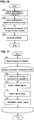
- Fig. 6 is a flowchart showing the overall procedure when carrying out the inspection.
- Fig. 7 is a flowchart showing the processing of a teaching step.
- Fig. 8 is a flowchart showing the processing when preparing an approximation surface of the wiring pattern on the substrate 25 prior to the application of solder.
- Fig. 9 is a flowchart showing the processing when preparing an approximation surface of the lands on the substrate 25 prior to the application of solder.
- Fig. 10 is a flowchart showing the processing when calculating an offset.
- Fig. 11 is a flowchart showing the processing in an inspection step.
- Fig. 12 is a function block diagram showing the functionality of the CPU 44 when carrying out the inspection. The following explanations make reference to Figs. 6 to 12 .
- the three-dimensional shape measurement apparatus 10 receives an input of substrate information, such as the name of the substrate 25 or the size of the substrate 25, from the RAM 45. Moreover, it receives an input of information on an inspection block, which is the region on the substrate 25 in which an inspection is to be carried out (Step S11 in Fig. 6 ; in the following "Step" may be omitted).
- the CPU 44 serves as a design information obtaining function 50.
- a substrate 25 to which solder has not yet been applied that is, the bare board (raw substrate) as shown in Fig. 3 is conveyed by the conveyor unit 14 to a predetermined position (S12), and a teaching step is carried out (S13). In the teaching step, a reference for measuring the height of the solder 29 is set. The specifics of this teaching step are explained later.
- solder 29 is applied.
- a substrate 25 to which solder has been applied is conveyed by the conveyor unit 14 to a predetermined position (S14), and the height of the solder 29 is inspected (S15). The specifics of this inspection are explained later.
- the processing of these Steps S14 to S15 is repeated for each substrate.
- FIG. 13 is a diagram showing an example of a partitioned inspection block 35. As shown in Fig. 13 , the inspection block 35 includes a wiring pattern 35a and lands 35c.
- FIG. 14 is a diagram schematically showing a cross-section taken in the thickness direction of the substrate, and shows an example of a substrate 49a, for which a surface approximated to a plane is prepared.
- Fig. 15 is a diagram schematically showing a cross-section taken in the thickness direction of the substrate, and shows an example of a substrate 49b, for which a surface approximated to a curved surface is prepared. As shown in Fig. 15 , in the case of a curved surface, some minor bending and flexing or the like occurs in the substrate 49b. This minor bending and flexing occurs if the range of the image of the substrate covered by the one inspection block 35 is broad. In this embodiment, a curved surface is employed, and a curved approximation surface is prepared as the approximation surface.
- an approximation surface of the lands is prepared (S23) for the inspection block 35.
- the approximation surface SI of the lands is expressed by the following equation. Note that “a” to “e” and “g” are coefficients, and “a” to “e” are the same coefficients as for the approximation surface Sr of the wiring pattern.
- z ax 2 + by 2 + cxy + dx + ey + g
- the approximation surface Sr of the wiring pattern and the approximation surface SI of the lands are regarded as parallel.
- the specifics of the process of preparing the approximation surface of the lands are explained further below.
- the offset is calculated (S24). This offset is a value that is used when measuring the height of the solder 29. Then, the calculated offset is stored in the RAM 45 (S25). The specifics of the process of calculating the offset are explained further below. The processing of these Steps S22 to S25 is repeated for each of the plurality of inspection blocks.
- FIG. 8 is a diagram showing the state in which the region 35a of the wiring pattern has been extracted from the inspection block 35. As shown in Fig. 16 , the region 35a of the wiring pattern is hatched. Then, regions for offset calculation are selected from the extracted region 35a of the wiring pattern.
- Fig. 16 is a diagram showing the state in which the region 35a of the wiring pattern has been extracted from the inspection block 35. As shown in Fig. 16 , the region 35a of the wiring pattern is hatched. Then, regions for offset calculation are selected from the extracted region 35a of the wiring pattern.
- FIG. 17 is a diagram showing the state in which regions 35b for offset calculation have been selected from the extracted region 35a of the wiring pattern in Fig. 16 .
- These regions 35b for offset calculation are hatched in Fig. 17 .
- regions are selected that are arranged around the lands 35c.
- regions that are close to the lands 35c in the inspection block 35 but also regions that are further away from the lands 35c are selected.
- they are selected such that six loci are included. That is to say, they are selected such that the conditions for preparing an approximation surface are satisfied.
- the heights of the selected regions 35b for offset calculation are measured (S34).
- the CPU 44 serves as a region height measurement means, and the regions 35b for the offset calculation serve as predetermined regions.
- the coefficients (a to f) of the approximation surface Sr of the wiring pattern are calculated (S35).
- the coordinates (x, y) are the values on the image when picked up with the image pickup unit 12, and the coordinate (z) is the value measured in S34.
- the approximation surface Sr of the wiring pattern is prepared. That is to say, the approximation surface Sr of the wiring pattern expresses a height distribution of the wiring pattern.
- the CPU 44 serves as an approximation surface calculation function 56, that is, as a distribution calculation means.
- Fig. 9 is a diagram showing a state in which the land regions 35c have been extracted from the inspection block 35.
- the land regions 35c are shown hatched in Fig. 18 .
- the heights of the extracted land regions 35c are measured (S43).
- the CPU 44 serves as a land height measurement means.
- the coefficients (a to e), which are the same as the coefficients (a to f) of the approximation surface Sr of the wiring pattern, are read out (S44), and using the position of the extracted land regions 35c, that is, the coordinates (x, y, z) indicating the x-position, the y-position and the z-position, the coefficient (g) of the approximation surface SI of the lands is calculated (S45).
- the coordinates (x, y) are the values on the image when picked up with the image pickup unit 12, and the coordinate (z) is the value measured in S43.
- the approximation surface SI of the lands is prepared.
- the coefficients other than the coefficient (f) indicating the height direction of the approximation surface Sr of the wiring pattern are the same for the approximation surface SI of the lands, and the approximation surface Sr of the wiring pattern is parallel to the approximation surface SI of the lands.
- the coefficients (a to f) of the approximation surface Sr of the wiring pattern calculated in S35 are read in (S51).
- the coefficients (a to e, g) of the approximation surface SI of the lands calculated in S44 and S45 are read in (S52).
- the distance (difference) between the approximation surface Sr of the wiring pattern and the approximation surface SI of the lands is calculated (S53). This distance is taken as the offset (OffL), and the offset is stored in the RAM 45 (S54).
- Fig. 19 is a diagram schematically showing a cross-section taken along the thickness direction of the substrate 25, where the approximation surface Sr of the wiring pattern is indicated as a double-dot-dashed line, the approximation surface SI of the lands is indicated as triple-dot-dashed line, and the distance OffL indicates the offset. As shown in Fig.
- the approximation surface Sr of the wiring pattern (distribution of heights of the wiring pattern) is calculated for the regions 35b for offset calculation of the wiring pattern, and the approximation surface SI of the lands (distribution of heights of the lands) is calculated for the regions 35c of the lands.
- solder 29 is applied to the substrate 25.
- the substrate 25 to which the solder has been applied is conveyed in S14, and the inspection blocks are obtained at the same positions as in S12 of Fig. 12 (S61).
- the inspection blocks include a measurement point P on the applied solder 29, for example.
- Fig. 20 is a diagram that schematically shows a cross section of an inspection block of the substrate 25, taken along the thickness direction, and is a z-x cross-sectional view through the measurement point P on the solder 29.
- the approximation surface SR of the wiring pattern is prepared by measuring the height of the wiring pattern (S62).
- the specifics of the method for preparing the approximation surface SR of the wiring pattern are the same as in Fig. 8 described above, so that further explanations are omitted.
- the CPU 44 serves as a wiring height measurement means and a curved approximation surface calculation means.
- the approximation surface SR of the wiring pattern is indicated by a dotted line.
- the approximation surface SL of the lands is parallel to the approximation surface SR of the wiring pattern, and is indicated by a dot-dashed line.
- a solder region is extracted from the inspection block (S63), and the offset (OffL) that was stored in the RAM 45 in S54 is read out (S64).
- the CPU 44 serves as a solder extraction function 55 and as a land offset read-in function 62.
- the height of the solder 29 in the extracted solder region is calculated (S65).
- the CPU 44 serves as a height measurement function 57 and a land offset subtracting function 59, that is, as a solder height calculation means. Based on the calculated result, it is inspected whether the solder quality is good or poor.
- the CPU 44 serves as an inspection function 60.
- Fig. 21 is a z-x cross-sectional view at the measurement point P, similar to Fig. 20 .
- the x-axis indicates the horizontal direction in the paper plane (main scanning direction)
- the z-axis denotes the height direction
- the y-axis denotes the direction out of the paper plane (secondary scanning direction).
- A denotes the point of intersection between the approximation surface SR of the wiring pattern and the line I through the measurement point P and the image pickup unit 12
- B denotes the point of intersection between the approximation surface SL of the lands and the line I
- C denotes the point of intersection between a height of zero, that is, between the x-axis and the line I.
- the x-position and the y-position of the points A, P, B and C are taken as the coordinates (Xp, Yp).
- the length of AC is calculated.
- the point A is a point on the approximation surface SR of the wiring pattern, so that (Xp, Yp) is inserted into (x, y), and the length of AC is calculated by the following equation.
- Za aXp 2 + bYp 2 + cXpYp + dXp + eYp + f
- Za is the length of AC.
- the length of PC is calculated. That is to say, the height of the measurement point P is measured.
- the measurement point P is a point on the solder 29, and this solder 29 is applied on the land 35c. Consequently, the height of the measurement point P is the height of the land 35c, which includes the solder 29.
- the CPU 44 serves as a solder land height measurement means.
- Fig. 22 is a diagram showing a magnification of the portion of the solder 29 and the land 35c in Fig. 21 , and is a diagram showing the tangent La and the angle ⁇ .
- the tangent La is the tangent at the coordinate (Xp, Yp), so that the inclination of the tangent La (tan ⁇ ) can be obtained by partially differentiating the equation of the approximation surface SR of the wiring pattern, and inserting (Xp, Yp) for (x, y).
- Lp is the line through the measurement point P and parallel to the tangents La and Lb
- Lt is the line through the point A and perpendicular to La
- M is the point of intersection between Lp and Lt
- N is the point of intersection between Lb and Lt.
- Fig. 23 is a diagram showing the intersection points M and N.
- the length of AN is the value of OffL that has been read out in S64
- the length of AM is AP cos ⁇
- the length of AP can be calculated as AC - PC.
- the three-dimensional shape measurement apparatus 10 calculates the height distribution in a predetermined region based on the height of a predetermined region, here, the height of the wiring pattern, and calculates the distance (offset) between this calculated height distribution and the height of the lands.
- the height distribution in the predetermined region reflects the change due to this warping or flexing. As a result, the influence of distortions of the substrate 25 on the calculated distance is suppressed.
- the offset is a value that is calculated in consideration of both the wiring pattern and the lands, so that it is not calculated only from the wiring pattern, as conventionally, and the height of the solder 29 can be calculated more accurately.
- the offset is calculated for the substrate 25 prior to the application of solder, and the approximation surface of the substrate 25 is calculated again for the wiring pattern with the substrate 25 after the application of solder, and then the height of the solder 29 is measured. Consequently, even when there is a change between the state of the substrate 25 prior to the application of solder and the state of the substrate 25 after the application of solder, the height of the solder 29 can be calculated accurately.
- the warping or flexing of the substrate 25 differs among different substrates 25.
- an offset was calculated by picking up an image with the image pickup unit 12 to measure the height of the wiring pattern and the height of the lands, and this calculated offset was used to calculate the height of the solder, but there is no limitation to this, and it is also possible to calculate the height of the solder by letting a user set an offset value in advance, and using the offset value set in this manner, for example.
- the present invention can be used advantageously whenever it is necessary to measure the height of solder.
- 10 three-dimensional shape measurement apparatus, 11 ... light-projecting unit, 12 .. image pickup unit, 13 ... image analysis / driver control unit, 14 ... conveyor unit, 15 .. measurement object, 16 ... region irradiated by light pattern, 17 ... region not irradiated by light pattern, 22 ... light source, 24 ... projection lens, 25, 49a, 49b ... substrate, 25a ... surface, 26 ... pattern generation element, 27 ... beam divider unit, 29 ... solder, 30 ... lands, 31 ... wiring pattern, 32 ... through hole, 33 ... serial number, 34 ... resist, 35 ... inspection block, 35a ... region of wiring pattern, 35b ... region for offset calculation, 35c ... region of lands, 40 ...
Landscapes
- Physics & Mathematics (AREA)
- General Physics & Mathematics (AREA)
- General Health & Medical Sciences (AREA)
- Chemical & Material Sciences (AREA)
- Analytical Chemistry (AREA)
- Biochemistry (AREA)
- Life Sciences & Earth Sciences (AREA)
- Health & Medical Sciences (AREA)
- Immunology (AREA)
- Pathology (AREA)
- Engineering & Computer Science (AREA)
- Computer Vision & Pattern Recognition (AREA)
- Length Measuring Devices By Optical Means (AREA)
- Image Processing (AREA)
- Image Analysis (AREA)
Claims (2)
- 3D-Formmessvorrichtung (10) zum Messen der dreidimensionalen Form eines Elements auf einem Substrat (25), das zumindest eine Anschlussfläche aufweist, die einem Bereich entspricht, auf welchem Lötzinn (29) aufbringbar ist, durch Analysieren eines auf das Element projizierten Lichtmusters; wobei die 3D-Formmessvorrichtung (10) aufweist:eine Lichtprojektionseinheit (11) zum Projizieren des Lichtmusters auf die Oberfläche des Elements auf dem Substrat (25),ein Bildaufnahmemittel (12) zum Aufnehmen eines Bildes eines Elements auf dem Substrat, auf welches das Lichtmuster projiziert wird,eine zentrale Verarbeitungseinheit (44), die eingerichtet ist, die 3D-Formmessvorrichtung (10) zu betreiben, um:eine Höhe eines vorgegebenen Bereichs aus einer vorgegebenen Referenzebene anhand eines ersten, durch das Bildaufnahmemittel (12) erlangten Bildes zu messen, wobei das Bild den vorgegebenen Bereich vor dem Aufbringen des Lötzinns (29) auf der Anschlussfläche aufweist;eine Höhenverteilung eines Verkabelungsmusters auf dem Substrat (25) in dem vorgegebenen Bereich anhand der gemessenen Höhe des vorgegebenen Bereichs zu berechnen;eine Höhe einer Anschlussfläche aus der vorgegebenen Referenzebene anhand des ersten, durch das Bildaufnahmemittel (12) erlangten Bildes zu messen, wobei das Bild die Anschlussfläche innerhalb des vorgegebenen Bereichs vor dem Aufbringen des Lötzinns (29) aufweist;einen ersten Abstand zwischen der Höhenverteilung des Verkabelungsmusters auf dem Substrat (25) in dem vorgegebenen Bereich und der gemessenen Höhe der Anschlussfläche zu berechnen;den berechneten ersten Abstand zu speichern;eine zweite Höhe des Verkabelungsmusters anhand eines zweiten, durch das Bildaufnahmemittel (12) erlangten Bildes zu messen, wobei das zweite Bild das Verkabelungsmuster des Substrats nach dem Aufbringen des Lötzinns aufweist;eine Näherungsoberfläche des Substrats (25) bei dem Verkabelungsmuster anhand der gemessenen zweiten Höhe des Verkabelungsmusters zu berechnen;eine Höhe der das Lötzinn umfassenden Anschlussfläche anhand eines zweiten, durch das Aufnahmemittel (12) erlangten Bilds zu messen, wobei das zweite Bild das auf die Anschlussfläche auf dem Substrat (25) aufgebrachte Lötzinn (29) aufweist,einen zweiten Abstand zwischen der berechneten Näherungsoberfläche des Substrats (25) bei dem Verkabelungsmuster und der gemessenen Höhe der das Lötzinn (29) umfassenden Anschlussfläche zu berechnen, undeine Höhe des auf die Anschlussfläche des Substrats (25) aufgebrachten Lötzinns (29) unter Verwendung des ersten Abstands und des zweiten Abstands zu berechnen.
- 3D-Formmessverfahren zum Messen der dreidimensionalen Form eines Elements auf einem Substrat, das zumindest eine Anschlussfläche aufweist, welches einem Bereich entspricht, auf welchem Lötzinn (29) aufbringbar ist, wobei das Verfahren aufweist:einen Schritt eines Projizierens eines Lichtmusters auf die Oberfläche des Elements auf dem Substrat (25);ein Schritt eines Aufnehmens eines Bilds eines Elements auf dem Substrat, auf welchem das Lichtmuster projiziert wird;einen Schritt eines Messens einer Höhe eines vorgegebenen Bereichs aus einer vorgegebenen Referenzebene anhand eines ersten, durch das Bildaufnahmemittel (12) erlangten Bildes, wobei das erste Bild den vorgegebenen Bereich vor einem Aufbringen von Lötzinn (29) auf der Anschlussfläche aufweist;einen Schritt eines Berechnens einer Höhenverteilung eines Verkabelungsmusters des Substrats (25) in dem vorgegebenen Bereich anhand der gemessenen Höhe des vorgegebenen Bereichs;einen Schritt eines Messens einer Höhe einer Anschlussfläche aus der vorgegebenen Referenzebene anhand des ersten, durch das Bildaufnahmemittel (12) erlangten Bildes, wobei das Bild die Anschlussfläche innerhalb des vorgegebenen Bereichs vor dem Aufbringen des Lötzinns (29) aufweist;einen Schritt eines Berechnens eines ersten Abstands zwischen der Höhenverteilung des Verkabelungsmusters auf dem Substrat (25) in dem vorgegebenen Bereich und der gemessenen Höhe der Anschlussfläche;einen Schritt eines Speicherns des berechneten ersten Abstands;einen Schritt eines Messens einer Höhe des Verkabelungsmusters in dem vorgegebenen Bereich von einem zweiten Bild, wobei das Bild das Verkabelungsmuster des Substrats nach dem Aufbringen des Lötzinns aufweist;einen Schritt eines Berechnens einer Näherungsoberfläche des Substrats (25) bei dem Verkabelungsmuster anhand der von dem Bild gemessenen Höhe des Verkabelungsmusters;einen Schritt eines Messens einer Höhe der das Lötzinn (29) umfassenden Anschlussfläche von dem zweiten Bild, wobei das Bild das auf der Anschlussfläche des Substrats (25) aufgebrachte Lötzinn (29) aufweist;einen Schritt eines Berechnens eines zweiten Abstands zwischen der berechneten Näherungsoberfläche des Substrats (25) bei dem Verkabelungsmuster und der gemessenen Höhe der das Lötzinn (29) umfassenden Anschlussfläche; undeinen Schritt eines Berechnens einer Höhe des auf der Anschlussfläche des Substrats (25) aufgebrachten Lötzinns (29) unter Verwendung des gespeicherten ersten Abstands und des berechneten zweiten Abstands.
Applications Claiming Priority (1)
| Application Number | Priority Date | Filing Date | Title |
|---|---|---|---|
| JP2011040511A JP5772062B2 (ja) | 2011-02-25 | 2011-02-25 | 三次元形状計測装置、および三次元形状計測方法 |
Publications (2)
| Publication Number | Publication Date |
|---|---|
| EP2492633A1 EP2492633A1 (de) | 2012-08-29 |
| EP2492633B1 true EP2492633B1 (de) | 2019-03-06 |
Family
ID=45524239
Family Applications (1)
| Application Number | Title | Priority Date | Filing Date |
|---|---|---|---|
| EP11186829.5A Not-in-force EP2492633B1 (de) | 2011-02-25 | 2011-10-27 | Verfahren und Vorrichtung für dreidimensionale Formvermessung |
Country Status (4)
| Country | Link |
|---|---|
| US (1) | US20120218562A1 (de) |
| EP (1) | EP2492633B1 (de) |
| JP (1) | JP5772062B2 (de) |
| KR (1) | KR20120098386A (de) |
Families Citing this family (3)
| Publication number | Priority date | Publication date | Assignee | Title |
|---|---|---|---|---|
| KR101614061B1 (ko) * | 2012-03-29 | 2016-04-20 | 주식회사 고영테크놀러지 | 조인트 검사 장치 |
| US20140293011A1 (en) * | 2013-03-28 | 2014-10-02 | Phasica, LLC | Scanner System for Determining the Three Dimensional Shape of an Object and Method for Using |
| DE102015121673B4 (de) * | 2015-12-11 | 2019-01-10 | SmartRay GmbH | Formermittlungsverfahren |
Family Cites Families (17)
| Publication number | Priority date | Publication date | Assignee | Title |
|---|---|---|---|---|
| US4876455A (en) * | 1988-02-25 | 1989-10-24 | Westinghouse Electric Corp. | Fiber optic solder joint inspection system |
| US5028799A (en) * | 1988-08-01 | 1991-07-02 | Robotic Vision System, Inc. | Method and apparatus for three dimensional object surface determination using co-planar data from multiple sensors |
| JP3314406B2 (ja) * | 1992-04-24 | 2002-08-12 | 松下電器産業株式会社 | クリーム半田の高さ測定方法 |
| US5465152A (en) * | 1994-06-03 | 1995-11-07 | Robotic Vision Systems, Inc. | Method for coplanarity inspection of package or substrate warpage for ball grid arrays, column arrays, and similar structures |
| US5995232A (en) * | 1997-07-14 | 1999-11-30 | U.S. Philips Corporation | Method of and device for inspecting a PCB |
| US6750899B1 (en) * | 2000-01-07 | 2004-06-15 | Cyberoptics Corporation | Solder paste inspection system |
| US6496270B1 (en) * | 2000-02-17 | 2002-12-17 | Gsi Lumonics, Inc. | Method and system for automatically generating reference height data for use in a three-dimensional inspection system |
| JP2002098513A (ja) * | 2000-09-22 | 2002-04-05 | Tani Denki Kogyo Kk | レーザ光を利用した画像認識による計測方法および計測装置 |
| JP3850282B2 (ja) * | 2001-12-12 | 2006-11-29 | 松下電器産業株式会社 | パターン面自動抽出方法及びそれを用いた形状計測装置 |
| JP2004292409A (ja) * | 2003-03-28 | 2004-10-21 | Sumitomo Chem Co Ltd | クロロシラン化合物の製造方法 |
| JP3868917B2 (ja) * | 2003-03-31 | 2007-01-17 | シーケーディ株式会社 | 三次元計測装置及び検査装置 |
| JP4746841B2 (ja) * | 2004-01-23 | 2011-08-10 | ルネサスエレクトロニクス株式会社 | 半導体集積回路装置の製造方法 |
| JP4613644B2 (ja) * | 2005-03-09 | 2011-01-19 | パナソニック株式会社 | 回路実装基板の外観検査方法 |
| JP4735010B2 (ja) * | 2005-04-06 | 2011-07-27 | パナソニック株式会社 | 基板高さ計測方法 |
| US7545512B2 (en) * | 2006-01-26 | 2009-06-09 | Koh Young Technology Inc. | Method for automated measurement of three-dimensional shape of circuit boards |
| JP4992811B2 (ja) * | 2008-04-18 | 2012-08-08 | パナソニック株式会社 | 電子部品実装装置 |
| JP4892602B2 (ja) * | 2009-10-30 | 2012-03-07 | ルネサスエレクトロニクス株式会社 | 半導体集積回路装置の製造方法 |
-
2011
- 2011-02-25 JP JP2011040511A patent/JP5772062B2/ja active Active
- 2011-10-10 KR KR1020110102792A patent/KR20120098386A/ko not_active Abandoned
- 2011-10-25 US US13/280,566 patent/US20120218562A1/en not_active Abandoned
- 2011-10-27 EP EP11186829.5A patent/EP2492633B1/de not_active Not-in-force
Non-Patent Citations (1)
| Title |
|---|
| None * |
Also Published As
| Publication number | Publication date |
|---|---|
| EP2492633A1 (de) | 2012-08-29 |
| JP2012177611A (ja) | 2012-09-13 |
| KR20120098386A (ko) | 2012-09-05 |
| JP5772062B2 (ja) | 2015-09-02 |
| US20120218562A1 (en) | 2012-08-30 |
Similar Documents
| Publication | Publication Date | Title |
|---|---|---|
| KR102918236B1 (ko) | 부품 검사 동안의 기준 오정렬 보상 | |
| US6496270B1 (en) | Method and system for automatically generating reference height data for use in a three-dimensional inspection system | |
| JP4901903B2 (ja) | 三次元検査システム | |
| JP5307876B2 (ja) | 検査方法 | |
| US10841561B2 (en) | Apparatus and method for three-dimensional inspection | |
| KR100522560B1 (ko) | 수직 슬라이스 이미징을 이용한 검사 방법 | |
| EP2492633B1 (de) | Verfahren und Vorrichtung für dreidimensionale Formvermessung | |
| KR102289322B1 (ko) | 배선기판 설계 지원장치, 배선기판 비아 배치방법 및 배선기판 비아 배치 프로그램 | |
| JP2008196974A (ja) | 突起物の高さ測定装置及び高さ測定方法 | |
| KR101121992B1 (ko) | 실장 검사 데이터 형성방법, 이를 저장한 저장매체 및 이를 이용하는 검사장치 | |
| KR101169982B1 (ko) | 기판 검사방법 | |
| KR101158324B1 (ko) | 형상 검사장치 | |
| JP6936577B2 (ja) | 位置ずれ量取得装置、検査装置、位置ずれ量取得方法および検査方法 | |
| JP3857668B2 (ja) | パターンの位置合わせ方法 | |
| JP2005030793A (ja) | 基板検査装置および検査方法 | |
| JP2006317408A (ja) | 反り検査装置 | |
| JP2002098513A (ja) | レーザ光を利用した画像認識による計測方法および計測装置 | |
| KR101311809B1 (ko) | 기판 검사방법 | |
| KR100719352B1 (ko) | 표면형상 측정방법 | |
| KR20150056148A (ko) | 검사 효율이 향상된 엑스레이 검사 장치 및 엑스레이 검사 방법 | |
| JP5851200B2 (ja) | 基板検査装置、基板検査方法および基板検査プログラム | |
| JP4034325B2 (ja) | 三次元計測装置及び検査装置 | |
| CN102261897B (zh) | 检查设备和检查方法 | |
| KR101262242B1 (ko) | 형상 검사방법 및 형상 검사장치 | |
| JP4760072B2 (ja) | X線検査装置及びx線検査方法 |
Legal Events
| Date | Code | Title | Description |
|---|---|---|---|
| PUAI | Public reference made under article 153(3) epc to a published international application that has entered the european phase |
Free format text: ORIGINAL CODE: 0009012 |
|
| AK | Designated contracting states |
Kind code of ref document: A1 Designated state(s): AL AT BE BG CH CY CZ DE DK EE ES FI FR GB GR HR HU IE IS IT LI LT LU LV MC MK MT NL NO PL PT RO RS SE SI SK SM TR |
|
| AX | Request for extension of the european patent |
Extension state: BA ME |
|
| 17P | Request for examination filed |
Effective date: 20130206 |
|
| 17Q | First examination report despatched |
Effective date: 20160802 |
|
| STAA | Information on the status of an ep patent application or granted ep patent |
Free format text: STATUS: EXAMINATION IS IN PROGRESS |
|
| GRAP | Despatch of communication of intention to grant a patent |
Free format text: ORIGINAL CODE: EPIDOSNIGR1 |
|
| STAA | Information on the status of an ep patent application or granted ep patent |
Free format text: STATUS: GRANT OF PATENT IS INTENDED |
|
| RAP1 | Party data changed (applicant data changed or rights of an application transferred) |
Owner name: OMRON CORPORATION |
|
| INTG | Intention to grant announced |
Effective date: 20180927 |
|
| GRAS | Grant fee paid |
Free format text: ORIGINAL CODE: EPIDOSNIGR3 |
|
| GRAA | (expected) grant |
Free format text: ORIGINAL CODE: 0009210 |
|
| STAA | Information on the status of an ep patent application or granted ep patent |
Free format text: STATUS: THE PATENT HAS BEEN GRANTED |
|
| AK | Designated contracting states |
Kind code of ref document: B1 Designated state(s): AL AT BE BG CH CY CZ DE DK EE ES FI FR GB GR HR HU IE IS IT LI LT LU LV MC MK MT NL NO PL PT RO RS SE SI SK SM TR |
|
| REG | Reference to a national code |
Ref country code: GB Ref legal event code: FG4D |
|
| REG | Reference to a national code |
Ref country code: CH Ref legal event code: EP Ref country code: AT Ref legal event code: REF Ref document number: 1105151 Country of ref document: AT Kind code of ref document: T Effective date: 20190315 |
|
| REG | Reference to a national code |
Ref country code: DE Ref legal event code: R096 Ref document number: 602011056821 Country of ref document: DE |
|
| REG | Reference to a national code |
Ref country code: IE Ref legal event code: FG4D |
|
| REG | Reference to a national code |
Ref country code: NL Ref legal event code: MP Effective date: 20190306 |
|
| REG | Reference to a national code |
Ref country code: LT Ref legal event code: MG4D |
|
| PG25 | Lapsed in a contracting state [announced via postgrant information from national office to epo] |
Ref country code: SE Free format text: LAPSE BECAUSE OF FAILURE TO SUBMIT A TRANSLATION OF THE DESCRIPTION OR TO PAY THE FEE WITHIN THE PRESCRIBED TIME-LIMIT Effective date: 20190306 Ref country code: NO Free format text: LAPSE BECAUSE OF FAILURE TO SUBMIT A TRANSLATION OF THE DESCRIPTION OR TO PAY THE FEE WITHIN THE PRESCRIBED TIME-LIMIT Effective date: 20190606 Ref country code: FI Free format text: LAPSE BECAUSE OF FAILURE TO SUBMIT A TRANSLATION OF THE DESCRIPTION OR TO PAY THE FEE WITHIN THE PRESCRIBED TIME-LIMIT Effective date: 20190306 Ref country code: LT Free format text: LAPSE BECAUSE OF FAILURE TO SUBMIT A TRANSLATION OF THE DESCRIPTION OR TO PAY THE FEE WITHIN THE PRESCRIBED TIME-LIMIT Effective date: 20190306 |
|
| PG25 | Lapsed in a contracting state [announced via postgrant information from national office to epo] |
Ref country code: GR Free format text: LAPSE BECAUSE OF FAILURE TO SUBMIT A TRANSLATION OF THE DESCRIPTION OR TO PAY THE FEE WITHIN THE PRESCRIBED TIME-LIMIT Effective date: 20190607 Ref country code: BG Free format text: LAPSE BECAUSE OF FAILURE TO SUBMIT A TRANSLATION OF THE DESCRIPTION OR TO PAY THE FEE WITHIN THE PRESCRIBED TIME-LIMIT Effective date: 20190606 Ref country code: RS Free format text: LAPSE BECAUSE OF FAILURE TO SUBMIT A TRANSLATION OF THE DESCRIPTION OR TO PAY THE FEE WITHIN THE PRESCRIBED TIME-LIMIT Effective date: 20190306 Ref country code: NL Free format text: LAPSE BECAUSE OF FAILURE TO SUBMIT A TRANSLATION OF THE DESCRIPTION OR TO PAY THE FEE WITHIN THE PRESCRIBED TIME-LIMIT Effective date: 20190306 Ref country code: HR Free format text: LAPSE BECAUSE OF FAILURE TO SUBMIT A TRANSLATION OF THE DESCRIPTION OR TO PAY THE FEE WITHIN THE PRESCRIBED TIME-LIMIT Effective date: 20190306 Ref country code: LV Free format text: LAPSE BECAUSE OF FAILURE TO SUBMIT A TRANSLATION OF THE DESCRIPTION OR TO PAY THE FEE WITHIN THE PRESCRIBED TIME-LIMIT Effective date: 20190306 |
|
| REG | Reference to a national code |
Ref country code: AT Ref legal event code: MK05 Ref document number: 1105151 Country of ref document: AT Kind code of ref document: T Effective date: 20190306 |
|
| PG25 | Lapsed in a contracting state [announced via postgrant information from national office to epo] |
Ref country code: SK Free format text: LAPSE BECAUSE OF FAILURE TO SUBMIT A TRANSLATION OF THE DESCRIPTION OR TO PAY THE FEE WITHIN THE PRESCRIBED TIME-LIMIT Effective date: 20190306 Ref country code: IT Free format text: LAPSE BECAUSE OF FAILURE TO SUBMIT A TRANSLATION OF THE DESCRIPTION OR TO PAY THE FEE WITHIN THE PRESCRIBED TIME-LIMIT Effective date: 20190306 Ref country code: RO Free format text: LAPSE BECAUSE OF FAILURE TO SUBMIT A TRANSLATION OF THE DESCRIPTION OR TO PAY THE FEE WITHIN THE PRESCRIBED TIME-LIMIT Effective date: 20190306 Ref country code: EE Free format text: LAPSE BECAUSE OF FAILURE TO SUBMIT A TRANSLATION OF THE DESCRIPTION OR TO PAY THE FEE WITHIN THE PRESCRIBED TIME-LIMIT Effective date: 20190306 Ref country code: AL Free format text: LAPSE BECAUSE OF FAILURE TO SUBMIT A TRANSLATION OF THE DESCRIPTION OR TO PAY THE FEE WITHIN THE PRESCRIBED TIME-LIMIT Effective date: 20190306 Ref country code: PT Free format text: LAPSE BECAUSE OF FAILURE TO SUBMIT A TRANSLATION OF THE DESCRIPTION OR TO PAY THE FEE WITHIN THE PRESCRIBED TIME-LIMIT Effective date: 20190706 Ref country code: CZ Free format text: LAPSE BECAUSE OF FAILURE TO SUBMIT A TRANSLATION OF THE DESCRIPTION OR TO PAY THE FEE WITHIN THE PRESCRIBED TIME-LIMIT Effective date: 20190306 Ref country code: ES Free format text: LAPSE BECAUSE OF FAILURE TO SUBMIT A TRANSLATION OF THE DESCRIPTION OR TO PAY THE FEE WITHIN THE PRESCRIBED TIME-LIMIT Effective date: 20190306 |
|
| PG25 | Lapsed in a contracting state [announced via postgrant information from national office to epo] |
Ref country code: PL Free format text: LAPSE BECAUSE OF FAILURE TO SUBMIT A TRANSLATION OF THE DESCRIPTION OR TO PAY THE FEE WITHIN THE PRESCRIBED TIME-LIMIT Effective date: 20190306 Ref country code: SM Free format text: LAPSE BECAUSE OF FAILURE TO SUBMIT A TRANSLATION OF THE DESCRIPTION OR TO PAY THE FEE WITHIN THE PRESCRIBED TIME-LIMIT Effective date: 20190306 |
|
| REG | Reference to a national code |
Ref country code: DE Ref legal event code: R097 Ref document number: 602011056821 Country of ref document: DE |
|
| PG25 | Lapsed in a contracting state [announced via postgrant information from national office to epo] |
Ref country code: AT Free format text: LAPSE BECAUSE OF FAILURE TO SUBMIT A TRANSLATION OF THE DESCRIPTION OR TO PAY THE FEE WITHIN THE PRESCRIBED TIME-LIMIT Effective date: 20190306 Ref country code: IS Free format text: LAPSE BECAUSE OF FAILURE TO SUBMIT A TRANSLATION OF THE DESCRIPTION OR TO PAY THE FEE WITHIN THE PRESCRIBED TIME-LIMIT Effective date: 20190706 |
|
| PLBE | No opposition filed within time limit |
Free format text: ORIGINAL CODE: 0009261 |
|
| STAA | Information on the status of an ep patent application or granted ep patent |
Free format text: STATUS: NO OPPOSITION FILED WITHIN TIME LIMIT |
|
| PG25 | Lapsed in a contracting state [announced via postgrant information from national office to epo] |
Ref country code: DK Free format text: LAPSE BECAUSE OF FAILURE TO SUBMIT A TRANSLATION OF THE DESCRIPTION OR TO PAY THE FEE WITHIN THE PRESCRIBED TIME-LIMIT Effective date: 20190306 |
|
| 26N | No opposition filed |
Effective date: 20191209 |
|
| PG25 | Lapsed in a contracting state [announced via postgrant information from national office to epo] |
Ref country code: SI Free format text: LAPSE BECAUSE OF FAILURE TO SUBMIT A TRANSLATION OF THE DESCRIPTION OR TO PAY THE FEE WITHIN THE PRESCRIBED TIME-LIMIT Effective date: 20190306 |
|
| PG25 | Lapsed in a contracting state [announced via postgrant information from national office to epo] |
Ref country code: TR Free format text: LAPSE BECAUSE OF FAILURE TO SUBMIT A TRANSLATION OF THE DESCRIPTION OR TO PAY THE FEE WITHIN THE PRESCRIBED TIME-LIMIT Effective date: 20190306 |
|
| PG25 | Lapsed in a contracting state [announced via postgrant information from national office to epo] |
Ref country code: MC Free format text: LAPSE BECAUSE OF FAILURE TO SUBMIT A TRANSLATION OF THE DESCRIPTION OR TO PAY THE FEE WITHIN THE PRESCRIBED TIME-LIMIT Effective date: 20190306 |
|
| REG | Reference to a national code |
Ref country code: CH Ref legal event code: PL |
|
| PG25 | Lapsed in a contracting state [announced via postgrant information from national office to epo] |
Ref country code: LI Free format text: LAPSE BECAUSE OF NON-PAYMENT OF DUE FEES Effective date: 20191031 Ref country code: CH Free format text: LAPSE BECAUSE OF NON-PAYMENT OF DUE FEES Effective date: 20191031 Ref country code: LU Free format text: LAPSE BECAUSE OF NON-PAYMENT OF DUE FEES Effective date: 20191027 |
|
| REG | Reference to a national code |
Ref country code: BE Ref legal event code: MM Effective date: 20191031 |
|
| PG25 | Lapsed in a contracting state [announced via postgrant information from national office to epo] |
Ref country code: BE Free format text: LAPSE BECAUSE OF NON-PAYMENT OF DUE FEES Effective date: 20191031 |
|
| GBPC | Gb: european patent ceased through non-payment of renewal fee |
Effective date: 20191027 |
|
| PG25 | Lapsed in a contracting state [announced via postgrant information from national office to epo] |
Ref country code: FR Free format text: LAPSE BECAUSE OF NON-PAYMENT OF DUE FEES Effective date: 20191031 Ref country code: GB Free format text: LAPSE BECAUSE OF NON-PAYMENT OF DUE FEES Effective date: 20191027 Ref country code: IE Free format text: LAPSE BECAUSE OF NON-PAYMENT OF DUE FEES Effective date: 20191027 |
|
| PG25 | Lapsed in a contracting state [announced via postgrant information from national office to epo] |
Ref country code: CY Free format text: LAPSE BECAUSE OF FAILURE TO SUBMIT A TRANSLATION OF THE DESCRIPTION OR TO PAY THE FEE WITHIN THE PRESCRIBED TIME-LIMIT Effective date: 20190306 |
|
| PG25 | Lapsed in a contracting state [announced via postgrant information from national office to epo] |
Ref country code: HU Free format text: LAPSE BECAUSE OF FAILURE TO SUBMIT A TRANSLATION OF THE DESCRIPTION OR TO PAY THE FEE WITHIN THE PRESCRIBED TIME-LIMIT; INVALID AB INITIO Effective date: 20111027 Ref country code: MT Free format text: LAPSE BECAUSE OF FAILURE TO SUBMIT A TRANSLATION OF THE DESCRIPTION OR TO PAY THE FEE WITHIN THE PRESCRIBED TIME-LIMIT Effective date: 20190306 |
|
| PG25 | Lapsed in a contracting state [announced via postgrant information from national office to epo] |
Ref country code: MK Free format text: LAPSE BECAUSE OF FAILURE TO SUBMIT A TRANSLATION OF THE DESCRIPTION OR TO PAY THE FEE WITHIN THE PRESCRIBED TIME-LIMIT Effective date: 20190306 |
|
| PGFP | Annual fee paid to national office [announced via postgrant information from national office to epo] |
Ref country code: DE Payment date: 20230830 Year of fee payment: 13 |
|
| REG | Reference to a national code |
Ref country code: DE Ref legal event code: R119 Ref document number: 602011056821 Country of ref document: DE |
|
| PG25 | Lapsed in a contracting state [announced via postgrant information from national office to epo] |
Ref country code: DE Free format text: LAPSE BECAUSE OF NON-PAYMENT OF DUE FEES Effective date: 20250501 |