EP2492588A1 - Solid state lighting assembly having a strain relief member - Google Patents
Solid state lighting assembly having a strain relief member Download PDFInfo
- Publication number
- EP2492588A1 EP2492588A1 EP20120156457 EP12156457A EP2492588A1 EP 2492588 A1 EP2492588 A1 EP 2492588A1 EP 20120156457 EP20120156457 EP 20120156457 EP 12156457 A EP12156457 A EP 12156457A EP 2492588 A1 EP2492588 A1 EP 2492588A1
- Authority
- EP
- European Patent Office
- Prior art keywords
- wire
- solid state
- cavity
- state lighting
- housing
- Prior art date
- Legal status (The legal status is an assumption and is not a legal conclusion. Google has not performed a legal analysis and makes no representation as to the accuracy of the status listed.)
- Granted
Links
- 239000007787 solid Substances 0.000 title claims abstract description 70
- 230000037431 insertion Effects 0.000 claims abstract description 27
- 238000003780 insertion Methods 0.000 claims abstract description 27
- 230000013011 mating Effects 0.000 claims abstract description 25
- 238000011144 upstream manufacturing Methods 0.000 claims abstract description 9
- 238000006073 displacement reaction Methods 0.000 claims description 2
- 238000009413 insulation Methods 0.000 claims description 2
- 239000000758 substrate Substances 0.000 description 35
- 239000004020 conductor Substances 0.000 description 8
- 230000010287 polarization Effects 0.000 description 6
- 230000007246 mechanism Effects 0.000 description 4
- 230000000712 assembly Effects 0.000 description 3
- 238000000429 assembly Methods 0.000 description 3
- 238000005476 soldering Methods 0.000 description 2
- 230000007704 transition Effects 0.000 description 2
- 230000001154 acute effect Effects 0.000 description 1
- 230000007717 exclusion Effects 0.000 description 1
- 239000004519 grease Substances 0.000 description 1
- 230000014759 maintenance of location Effects 0.000 description 1
- 239000000463 material Substances 0.000 description 1
- 230000000717 retained effect Effects 0.000 description 1
Images



Classifications
-
- H—ELECTRICITY
- H01—ELECTRIC ELEMENTS
- H01R—ELECTRICALLY-CONDUCTIVE CONNECTIONS; STRUCTURAL ASSOCIATIONS OF A PLURALITY OF MUTUALLY-INSULATED ELECTRICAL CONNECTING ELEMENTS; COUPLING DEVICES; CURRENT COLLECTORS
- H01R13/00—Details of coupling devices of the kinds covered by groups H01R12/70 or H01R24/00 - H01R33/00
- H01R13/58—Means for relieving strain on wire connection, e.g. cord grip, for avoiding loosening of connections between wires and terminals within a coupling device terminating a cable
- H01R13/5833—Means for relieving strain on wire connection, e.g. cord grip, for avoiding loosening of connections between wires and terminals within a coupling device terminating a cable the cable being forced in a tortuous or curved path, e.g. knots in cable
-
- H—ELECTRICITY
- H10—SEMICONDUCTOR DEVICES; ELECTRIC SOLID-STATE DEVICES NOT OTHERWISE PROVIDED FOR
- H10H—INORGANIC LIGHT-EMITTING SEMICONDUCTOR DEVICES HAVING POTENTIAL BARRIERS
- H10H20/00—Individual inorganic light-emitting semiconductor devices having potential barriers, e.g. light-emitting diodes [LED]
- H10H20/80—Constructional details
- H10H20/85—Packages
-
- F—MECHANICAL ENGINEERING; LIGHTING; HEATING; WEAPONS; BLASTING
- F21—LIGHTING
- F21V—FUNCTIONAL FEATURES OR DETAILS OF LIGHTING DEVICES OR SYSTEMS THEREOF; STRUCTURAL COMBINATIONS OF LIGHTING DEVICES WITH OTHER ARTICLES, NOT OTHERWISE PROVIDED FOR
- F21V27/00—Cable-stowing arrangements structurally associated with lighting devices, e.g. reels
- F21V27/02—Cable inlets
-
- F—MECHANICAL ENGINEERING; LIGHTING; HEATING; WEAPONS; BLASTING
- F21—LIGHTING
- F21V—FUNCTIONAL FEATURES OR DETAILS OF LIGHTING DEVICES OR SYSTEMS THEREOF; STRUCTURAL COMBINATIONS OF LIGHTING DEVICES WITH OTHER ARTICLES, NOT OTHERWISE PROVIDED FOR
- F21V19/00—Fastening of light sources or lamp holders
- F21V19/001—Fastening of light sources or lamp holders the light sources being semiconductors devices, e.g. LEDs
- F21V19/003—Fastening of light source holders, e.g. of circuit boards or substrates holding light sources
-
- F—MECHANICAL ENGINEERING; LIGHTING; HEATING; WEAPONS; BLASTING
- F21—LIGHTING
- F21Y—INDEXING SCHEME ASSOCIATED WITH SUBCLASSES F21K, F21L, F21S and F21V, RELATING TO THE FORM OR THE KIND OF THE LIGHT SOURCES OR OF THE COLOUR OF THE LIGHT EMITTED
- F21Y2113/00—Combination of light sources
- F21Y2113/10—Combination of light sources of different colours
- F21Y2113/13—Combination of light sources of different colours comprising an assembly of point-like light sources
-
- F—MECHANICAL ENGINEERING; LIGHTING; HEATING; WEAPONS; BLASTING
- F21—LIGHTING
- F21Y—INDEXING SCHEME ASSOCIATED WITH SUBCLASSES F21K, F21L, F21S and F21V, RELATING TO THE FORM OR THE KIND OF THE LIGHT SOURCES OR OF THE COLOUR OF THE LIGHT EMITTED
- F21Y2115/00—Light-generating elements of semiconductor light sources
- F21Y2115/10—Light-emitting diodes [LED]
Definitions
- the subject matter described herein relates generally to solid state lighting assemblies.
- Solid state lighting assemblies generally include a solid state lighting module having a substrate with a lighting element disposed thereon.
- the lighting element may be a light emitting diode (LED).
- the substrate includes contacts pads that are electrically coupled to the lighting element.
- the contact pads include a positive contact pad and a negative contact pad.
- the positive contact pad and the negative contact pad are configured to electrically couple to a positive wire and a negative wire, respectively.
- the positive wire and the negative wire form a circuit through the solid state lighting module to power the lighting element.
- soldered wires are soldered to the contact pads of the substrate. Soldering the wires to the contact pads generally requires special tools, extra materials, and an extra assembly step, which add to the overall cost of assembly. Additionally, soldering, over time and with handling of the components, may subject the assembly to improper electrical connections. Moreover, the soldered wires may be subject to becoming dislodged from the contact pads of the substrate. In particular, forces applied to the wires may disconnect the wires from the contact pad.
- the problem to be solved is a need remains for a solid state lighting assembly that enables quick and tool-less connections between the wires and the contact pads. Another need remains for a solid state lighting assembly that provides strain relief for the wires to prevent the wires from becoming disconnected from the contact pads.
- the solution is provided by a solid state lighting assembly.
- the assembly includes a housing configured to hold a solid state lighting module.
- the housing has a cavity.
- a contact is positioned within the cavity.
- the contact has a wire end and a mating end.
- the wire end is configured to be coupled to an insertion segment of a wire.
- the wire extends from the cavity to an exterior of the housing.
- a strain relief member extends from the exterior of the housing. The strain relief member is configured to engage a portion of the wire upstream from the insertion segment of the wire.
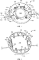
- Figure 1 is a top perspective view of a solid state lighting assembly formed in accordance with an embodiment.
- Figure 2 is a bottom perspective view of the solid state lighting assembly shown in Figure 1 .
- Figure 3 is a top perspective view of a solid state lighting module formed in accordance with an embodiment.
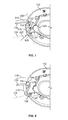
- Figure 4 is a partial top perspective view of the solid state lighting assembly shown in Figure 1 .
- Figure 5 is a partial cut-away view of the solid state lighting assembly shown in Figure 1 .
- Figure 6 is a top perspective view of a strain relief member formed in accordance with an embodiment.
- Figure 7 is a top perspective view of a strain relief member formed in accordance with another embodiment.
- Figure 8 is a top perspective view of a strain relief member formed in accordance with another embodiment.
- Figure 9 is a top perspective view of the solid state lighting assembly shown in Figure 1 and having an optic formed in accordance with an embodiment and coupled thereto.
- a solid state lighting assembly in one embodiment, includes a housing configured to hold a solid state lighting module.
- the housing has a cavity.
- a contact is positioned within the cavity.
- the contact has a wire end and a mating end.
- the wire end is configured to be coupled to a insertion segment of a wire.
- the wire extends from the cavity to an exterior of the housing.
- a strain relief member extends from the exterior of the housing. The strain relief member is configured to engage a portion of the wire upstream from the insertion segment of the wire.
- a solid state lighting assembly in another embodiment, includes a housing having a cavity.
- a contact is positioned within the cavity.
- the contact has a wire end and a mating end.
- the wire end is configured to be coupled to a insertion segment of a wire.
- the wire extends from the cavity to an exterior of the housing.
- the mating end of the contact has a tip and a mating interface remote from the tip. The tip engages the housing.
- a solid state lighting module is positioned within the housing.
- the solid state lighting module has a substrate having a contact pad disposed thereon. The mating interface of the contact engages the contact pad. The contact is flexed between the tip and the mating interface to spring bias the contact against the contact pad.
- a solid state lighting assembly in another embodiment, includes a housing configured to hold a solid state lighting module.
- the housing has a cavity having a cavity axis.
- a contact is positioned within the cavity.
- the contact has a wire end and a mating end.
- the wire end of the contact is formed as a poke-in wire connection having a barrel extending axially along the cavity axis and a barb extending into the barrel at an oblique angle with respect to the cavity axis.
- the barb engages a conductor of an insertion segment of a wire inserted into the barrel in a loading direction.
- the barb retains the insertion segment of the wire in the barrel in response to forces applied to the wire in a direction opposite to the loading direction.
- the wire extends from the cavity to an exterior of the housing.
- a strain relief member extends from the exterior of the housing. The strain relief member is configured to engage a portion of the wire upstream from the insertion segment of the wire.
- Embodiments described herein include a solid state lighting assembly having a tool-less connection between the wires and the contact pads of a solid state lighting module.
- the embodiments include a poke-in wire connection that receives wires configured to power a lighting element of the solid state lighting assembly.
- the poke-in wire connection includes a contact having a wire end that receives the wire and mating end that forms a separable, compressible interface with the contact pads of the solid state lighting module.
- the wire end of the contact includes a barb that engages the wire to oppose forces that may dislodge the wire from the contact.
- the solid state lighting assembly includes a strain relief member configured to engage the wire. The strain relief member further opposes forces that may dislodge the wire from the contact.
- FIG 1 is a top perspective view of a solid state lighting assembly 100 formed in accordance with an embodiment.
- the solid state lighting assembly 100 includes a housing 102 and a solid state lighting module 104.
- the solid state lighting module 104 includes a substrate 106 having a lighting element 108 disposed thereon.
- the lighting element 108 may be a light emitting diode (LED) or any other suitable solid state lighting element.
- the housing 102 includes a top 110 and an opposite bottom 112 (shown in Figure 2 ).
- An opening 114 extends through the housing 102 from the top 110 to the bottom 112.
- the opening 114 is generally centered within the housing 102. Alternatively, the opening 114 may extend through any portion of the housing 102.
- the substrate 106 of the solid state lighting module 104 is received in the bottom 112 of the housing 102.
- the substrate 106 is received in the housing 102 such that the lighting element 108 is positioned within the opening 114 of the housing 102.
- the lighting element 108 may extend through the opening 114 of the housing 102.
- the lighting element 108 emits light from the top 110 of the housing 102.
- the housing 102 includes recesses 116 formed around the opening 114.
- the recesses 116 may be configured to receive an optic 118, as illustrated in Figure 9 .
- the optic 118 directs the light emitted from the lighting element 108 in a particular lighting pattern.
- the cavities 120 are formed in the housing 102.
- the cavities 120 include an opening 122.
- the cavities 120 extend from the opening 122 into the housing 102.
- the cavities 120 extend along a cavity axis 124 from the opening 122 into the housing 102.
- the openings 122 of the cavities 120 may be formed proximate to an outer perimeter 126 of the housing 102.
- the openings 122 of the cavities 120 may be formed inward from the perimeter 126 of the housing 102.
- the openings 122 of the cavities 120 may be formed proximate to the opening 114 of the housing 102.
- the openings 122 of the cavities 120 face away from the opening 114 of the housing 102.
- the openings 122 of the cavities 120 may face toward the opening 114 of the housing 102 or at any suitable angle with respect to the opening 114 of the housing in alternative embodiments.
- the openings 122 of the cavities 120 are configured to receive a insertion segment 128 of a wire 130 therein.
- the insertion segment 128 of the wire 130 may include an exposed conductor 148 that is terminated within the cavity 120.
- the insertion segment 128 of the wire 130 is inserted into the cavity 120 along the cavity axis 124 in a loading direction 144.
- the wire 130 extends from the cavity 120 to an exterior 146 of the housing 102.
- the illustrated embodiment includes a positive cavity 120 and a negative cavity 120.
- the positive cavity 120 receives a positive wire 130 having a positive polarity.
- the negative cavity 120 receives a negative wire 130 having negative polarity.
- the opening 122 of the positive cavity 120 faces in a different direction than the opening 122 of the negative cavity 120.
- the opening 122 of the positive cavity 120 is illustrated facing in an opposite direction from the opening 122 of the negative cavity 120.
- the opening 122 of the positive cavity 120 and the opening 122 of the negative cavity 120 may face in other directions, including in the same direction.
- the wire 130 includes a downstream end 140 and an upstream end 142.
- the insertion segment 128 of the wire 130 is positioned at the downstream end 140 of the wire 130.
- the downstream end 140 of the wire 130 is received in the cavity 120.
- the upstream end 142 of the wire 130 extends from the housing 102 to another component, such as a driver or a power source (not shown).
- a strain relief member 150 extends from the exterior 146 of the housing 102.
- the strain relief member 150 may be coupled to the housing 102. In other embodiments the strain relief member 150 may be formed integrally with the housing 102.
- the strain relief member 150 is positioned spaced apart from the cavity 120. For example, the strain relief member 150 and the cavity 120 may be spaced apart a distance D 1 .
- the strain relief member 150 is positioned proximate to the perimeter 126 of the housing 102.
- the strain relief member 150 may be positioned inward from the perimeter 126 of the housing 102 in alternative embodiments. For example, the strain relief member 150 may be positioned proximate to the opening 114 of the housing 102.
- the strain relief member 150 is configured to engage a portion of the wire 130.
- the strain relief member 150 engages the wire 130 upstream from the insertion segment 128 of the wire 130.
- the strain relief member 150 provides resistance to forces applied to the wire 130.
- the strain relief member 150 provides resistance to forces that may tend to disengage the insertion segment 128 of the wire 130 from the cavity 120.
- the strain relief member 150 may resist forces on the wire 130 in a direction opposite to the loading direction 144 of the wire 130.
- the strain relief member 150 is a hook 152 (as described in more detail with respect to Figure 6 ).
- the strain relief member 150 may be a series of posts 154 (as described in more detail with respect to Figure 7 ) or a single post 156 (as described in more detail with respect to Figure 8 ).
- the strain relief member 150 may be any suitable member for resisting forces on the wire 130.
- a plurality of screws 158 extend through the housing 102 to secure the housing 102 to a heat sink (not shown).
- FIG. 2 is a bottom perspective view of the solid state lighting assembly 100.
- the solid state lighting assembly 100 includes a bottom 112.
- a solid state lighting module receptacle 160 is formed on the bottom 112 of the solid state lighting assembly 100.
- the receptacle 160 is sized to receive the substrate 106 of the solid state lighting module 104.
- the solid state lighting module 104 may be press-fit into the receptacle 160.
- the receptacle 160 includes retention mechanisms 162 to create an interference fit with the solid state lighting module 104.
- the receptacle 160 may include latches, grooves, notches, and/or any other suitable mechanism for securing the solid state lighting module 104 to the housing 102.
- the solid state lighting module 104 may be adhered or bonded to the housing 102. Recesses 164 may be formed in the receptacle 160 to enable the solid state lighting module 104 to be removed from the housing 102. In an alternative embodiment, the solid state lighting module 104 may be secured to the heat sink and the housing 102 may be loaded over the solid state lighting module 104.
- the screws 158 extend through the bottom 112 of the housing 102.
- the screws 158 are configured to couple the housing 102 to the heat sink (not shown), such that the solid state lighting module 104 is secured between the heat sink and the housing 102.
- the screws 158 extend through mounting locations 166 formed in the substrate 106 such that the screws 158 are not secured to the substrate 106.
- the screws 158 may be secured to the substrate 106.
- the housing 102 may include pins, posts, or the like extending therefrom to secure the housing 102 to the heat sink.
- the housing 102 also includes polarization features 169 to provide a keying mechanism for mounting the solid state lighting module 104 within the housing 102.
- Other polarization features 168 provide an alignment mechanism for mounting the solid state lighting assembly 100 to the heat sink.
- FIG 3 is a top perspective view of the solid state lighting module 104.
- the solid state lighting module 104 includes the substrate 106.
- the substrate 106 may be a circuit board, for example, a printed circuit board.
- the lighting element 108 is centered on the substrate 106. Alternatively, the lighting element 108 may be positioned at any suitable location on the substrate 106. As set forth above, the lighting element 108 may be a solid state lighting element, for example, an LED.
- the substrate 106 may include a single lighting element 108. In alternative embodiments, the substrate 106 may include multiple lighting elements 108.
- the multiple lighting elements 108 may include different colored lighting elements 108 so that a color of light emitted from the solid state lighting module 104 may be selectively adjusted and/or adjusted in a lighting sequence. In one embodiment, the lighting element 108 may be covered with a lens or the like.
- Contact pads 172 are provided on the substrate 106.
- the contact pads 172 are electrically conductive and configured to receive a power signal.
- the contact pads 172 are configured to electrically couple to the conductor 148 of a wire 130 (both shown in Figure 1 ).
- the contact pads 172 are electrically coupled to the lighting element 108 through a signal trace or the like.
- the contact pads 172 direct the power signal from a wire 130 to the lighting element 108.
- the illustrated embodiment includes a positive contact pad 174 and a negative contact pad 176.
- the positive contact pad 174 is configured to electrically couple to the positive wire 130 (shown in Figure 1 ).
- the negative contact pad 176 is configured to electrically couple to the negative wire 130 (shown in Figure 1 ).
- the substrate 106 includes a front 182 and a back 184.
- a pair of sides 186 extends between the front 182 and the back 184.
- the mounting locations 166 are formed in the front 182 and the back 184 of the substrate 106. Alternatively, the mounting locations 166 may be formed in the sides 186 of the substrate 106.
- Each of the front 182 and the back 184 of the substrate 106 includes a pair of mounting locations 166 separated by a distance D 2 .
- Each of the pair of mounting locations 166 is positioned a distance D 3 from the sides 186 of the substrate 106.
- each of the front 182 and the back 184 of the substrate 106 may include any number of mounting locations 166 spaced at any distance D 2 from each other or distance D 3 from the sides 186 of the substrate 106.
- the screws 158 (shown in Figure 1 ) are configured to extend through the mounting locations 166. In one embodiment, the screws 158 may be secured to the substrate 106 at the mounting locations 166.
- the sides 186 of the substrate 106 include polarization recesses 188 formed therein.
- polarization recesses 188 may be formed in the front 182 and/or back 184 of the substrate 106.
- the polarization recesses 188 are configured to receive the polarization features 169 of the housing 102 therethrough.
- Figure 4 is a partial top perspective view of the solid state lighting assembly 100.
- the housing 102 of the solid state lighting assembly 100 is illustrated in phantom to show an interior 198 of the cavity 120.
- a contact 190 is positioned within the cavity 120.
- the contact 190 is a poke-in wire contact configured to receive the conductor 148 of the wire 130.
- the contact 190 may be an insulation displacement connector, a crimp connector, or the like in alternative embodiments.
- the contact 190 includes a wire end 192 and a mating end 194.
- the mating end 194 of the contact 190 forms a separable, compressible interface with the contact pad 172 of the substrate 106.
- the wire end 192 of the contact 190 includes a barrel 196 that receives the conductor 148 of the wire 130.
- the barrel 196 extends through the cavity 120 along the cavity axis 124.
- the conductor 148 of the wire 130 is inserted into the barrel 196 in the loading direction 144.
- FIG. 5 is a partial cut-away view of the solid state lighting assembly 100.
- the wire end 192 of the contact 190 includes the barrel 196 and a barb 200.
- the barrel 196 extends from the opening 122 of the cavity 120 into the cavity 120 along the cavity axis 124.
- the barb 200 extends at an oblique angle with respect to the cavity axis 124.
- the term "oblique angle” is defined as any angle that diverges from a straight line.
- An "oblique angle” may be an acute angle, an obtuse angle, or a right angle.
- the barb 200 extends inward from the barrel 196 in the direction of the loading direction 144.
- a tip 202 of the barb 200 engages the wire 130.
- the tip 202 of the barb 200 engages the conductor 148 of the wire 130.
- the barb 200 retains the wire 130 in the barrel 196.
- the barb 200 is configured to oppose forces applied to the wire 130 in a direction opposite to the loading direction 144 of the wire 130.
- the conductor 148 of the wire 130 engages the wire end 192 of the contact 190.
- the mating end 194 of the contact 190 extends from the wire end 192 of the contact 190 such that power signals from the wire 130 are directed to the mating end 194 of the contact 190.
- the mating end 194 of the contact 190 extends from the barrel 196.
- the mating end 194 of the contact 190 is configured as a simply supported beam.
- the mating end 194 of the contact 190 includes a transition member 206 that is joined to the wire end 192 of the contact 190.
- a tip 208 of the mating end 194 of the contact 190 abuts the housing 102.
- a mating interface 210 of the mating end 194 of the contact 190 extends between the tip 208 and the transition member 206.
- the mating interface 210 is configured to engage the contact pad 172 of the substrate 106.
- the mating interface 210 forms separable, compressible interface with the contact pad 172 of the substrate 106.
- the contact 190 is flexed between the tip 208 of the mating end 194 and the mating interface 210 to spring bias the contact 190 against the contact pad 172.
- the thermal interface 170 is provided on the substrate 106.
- the thermal interface 170 may be any suitable thermal interface, for example conductive grease, for mounting the substrate 106 to a heat sink (not shown).
- Figure 6 is a top perspective view of a strain relief member 150 formed in accordance with an embodiment and having the wire 130 coupled thereto.
- Figure 6 illustrates the strain relief member 150 as a hook 152.
- the hook 152 is provided on the exterior 146 of the housing 102.
- the hook 152 may be coupled to the housing 102 or formed integrally therewith.
- the hook 152 includes a slot 214 to engage the wire 130 upstream from the insertion segment 128 of the wire 130.
- the wire 130 at least partially extends around the hook 152.
- the slot 214 may be sized to form an interference fit with the wire 130.
- the slot 214 faces in a different direction than the opening 122 of the cavity 120.
- the slot 214 faces in an opposite direction from the opening 122 of the cavity 120.
- the slot 214 and the opening 122 of the cavity 120 may face in the same direction.
- the wire 130 includes the insertion segment 128 extending from the cavity 120 to the exterior 146 of the housing 102.
- the insertion segment 128 generally extends along the cavity axis 124 of the cavity 120.
- a main segment 216 of the wire extends from the hook 152 to a power source (not shown).
- An intermediate segment 218 of the wire 130 extends between the main segment 216 of the wire 130 and the insertion segment 128 of the wire 130.
- the hook 152 engages the wire 130 such that the intermediate segment 218 of the wire 130 extends at an oblique angle with respect to the cavity axis 124.
- the hook 152 engages the wire 130 such that the main segment 216 of the wire 130 extends at an oblique angle with respect to the intermediate segment 218 of the wire 130.
- the main segment 216 of the wire 130 may extend from the hook 152 parallel to the cavity axis 124.
- the main segment 216 of the wire 130 may extend from the hook 152 at an oblique angle with respect to
- Figure 7 is a top perspective view of a strain relief member 150 formed in accordance with an embodiment and having the wire 130 coupled thereto.
- Figure 7 illustrates the strain relief member 150 as a series of posts 154.
- the posts 154 extend along a line 220.
- the illustrated embodiment includes three posts 154.
- Alternative embodiments may include any number of posts 154.
- the intermediate segment 218 of the wire 130 is threaded through the posts 154 such that intermediate segment 218 of the wire 130 changes directions at each post 154.
- the intermediate segment 218 of the wire 130 travels in a first direction 222 to a first post 154 and travels in a second direction 224 from the first post 154 to a second post 154.
- the intermediate segment 218 of the wire 130 at least partially wraps around each post 154.
- the intermediate segment 218 of the wire 130 may be entirely wrapped around each post 154 one or more times.
- the posts 154 may include a flange (not shown) extending from the top thereof.
- the intermediate segment 218 of the wire 130 may be held between the housing 102 and the flange.
- the flange may form an interference fit with the wire 130.
- the posts 154 may include grooves extending therearound to receive and position the intermediate segment 218 of the wire 130 with respect to the post 154.
- the posts 154 engage the wire 130 such that the intermediate segment 218 of the wire 130 extends at an oblique angle with respect to the cavity axis 124.
- the posts 154 engage the wire 130 such that the main segment 216 of the wire 130 extends at an oblique angle with respect to the intermediate segment 218 of the wire 130.
- the main segment 216 of the wire 130 may extend from the last post 154 parallel to the cavity axis 124.
- the main segment 216 of the wire 130 may extend from the last post 154 at an oblique angle with respect to the cavity axis 124.
- Figure 8 is a top perspective view of a strain relief member 150 formed in accordance with an embodiment and having the wire 130 coupled thereto.
- Figure 8 illustrates the strain relief member 150 as a post 156.
- the post 156 may be integrally formed with the housing 102.
- the post 156 may be a screw, pin, or the like that is inserted into the housing 102.
- the wire 130 is configured to wrap at least partially around the post 156.
- the wire 130 may be wrapped entirely around the post 156 one or more times.
- the post 156 includes a flange 226 extending from the top thereof.
- the intermediate segment 218 of the wire 130 may be held between the housing 102 and the flange 226.
- the flange 226 may form an interference fit with the wire 130.
- the post 156 may include grooves extending therearound to receive and position the intermediate segment 218 of the wire 130 with respect to the post 156.
- the post 156 engages the wire 130 such that the intermediate segment 218 of the wire 130 extends at an oblique angle with respect to the cavity axis 124.
- the post 156 engages the wire 130 such that the main segment 216 of the wire 130 extends at an oblique angle with respect to the intermediate segment 218 of the wire 130.
- the main segment 216 of the wire 130 may extend from the post 156 parallel to the cavity axis 124.
- the main segment 216 of the wire 130 may extend from the post 156 at an oblique angle with respect to the cavity axis 124.
- Figure 9 is a top perspective view of the solid state lighting assembly 100 having an optic 118 coupled thereto.
- the optic 118 includes a top 228 and a bottom 230.
- the bottom 230 of the optic 118 is coupled to the housing 102 of the solid state lighting assembly 100.
- the bottom 230 of the optic 118 includes protrusions 232 extending therefrom.
- the protrusions 232 are received in the recesses 116 of the housing 102.
- the protrusions 232 may be press-fit into the recesses 116 and/or retained within the recesses 116 through an interference fit.
- the housing 102 may include a latch, detent, or the like to retain the optic 118.
- the optic 118 may be adhered or bonded to the housing 102 or substrate 106.
- the optic 118 has a conical shape and extends outward from the bottom 230 of the optic 118 to the top 228 of the optic 118.
- the optic 118 is configured to direct and/or focus light emitted from the solid state lighting assembly 100.
Landscapes
- Engineering & Computer Science (AREA)
- General Engineering & Computer Science (AREA)
- Non-Portable Lighting Devices Or Systems Thereof (AREA)
- Arrangement Of Elements, Cooling, Sealing, Or The Like Of Lighting Devices (AREA)
- Led Device Packages (AREA)
- Fastening Of Light Sources Or Lamp Holders (AREA)
Abstract
Description
- The subject matter described herein relates generally to solid state lighting assemblies.
- Solid state lighting assemblies generally include a solid state lighting module having a substrate with a lighting element disposed thereon. For example, the lighting element may be a light emitting diode (LED). The substrate includes contacts pads that are electrically coupled to the lighting element. The contact pads include a positive contact pad and a negative contact pad. The positive contact pad and the negative contact pad are configured to electrically couple to a positive wire and a negative wire, respectively. The positive wire and the negative wire form a circuit through the solid state lighting module to power the lighting element.
- However, conventional solid state lighting assemblies are not without their disadvantages. Typically, the wires (positive and negative) are soldered to the contact pads of the substrate. Soldering the wires to the contact pads generally requires special tools, extra materials, and an extra assembly step, which add to the overall cost of assembly. Additionally, soldering, over time and with handling of the components, may subject the assembly to improper electrical connections. Moreover, the soldered wires may be subject to becoming dislodged from the contact pads of the substrate. In particular, forces applied to the wires may disconnect the wires from the contact pad.
- The problem to be solved is a need remains for a solid state lighting assembly that enables quick and tool-less connections between the wires and the contact pads. Another need remains for a solid state lighting assembly that provides strain relief for the wires to prevent the wires from becoming disconnected from the contact pads.
- The solution is provided by a solid state lighting assembly. The assembly includes a housing configured to hold a solid state lighting module. The housing has a cavity. A contact is positioned within the cavity. The contact has a wire end and a mating end. The wire end is configured to be coupled to an insertion segment of a wire. The wire extends from the cavity to an exterior of the housing. A strain relief member extends from the exterior of the housing. The strain relief member is configured to engage a portion of the wire upstream from the insertion segment of the wire.
- The invention will now be described by way of example with reference to the accompanying drawings in which:
-
Figure 1 is a top perspective view of a solid state lighting assembly formed in accordance with an embodiment. -
Figure 2 is a bottom perspective view of the solid state lighting assembly shown inFigure 1 . -
Figure 3 is a top perspective view of a solid state lighting module formed in accordance with an embodiment. -
Figure 4 is a partial top perspective view of the solid state lighting assembly shown inFigure 1 . -
Figure 5 is a partial cut-away view of the solid state lighting assembly shown inFigure 1 . -
Figure 6 is a top perspective view of a strain relief member formed in accordance with an embodiment. -
Figure 7 is a top perspective view of a strain relief member formed in accordance with another embodiment. -
Figure 8 is a top perspective view of a strain relief member formed in accordance with another embodiment. -
Figure 9 is a top perspective view of the solid state lighting assembly shown inFigure 1 and having an optic formed in accordance with an embodiment and coupled thereto. - In one embodiment, a solid state lighting assembly is provided. The assembly includes a housing configured to hold a solid state lighting module. The housing has a cavity. A contact is positioned within the cavity. The contact has a wire end and a mating end. The wire end is configured to be coupled to a insertion segment of a wire. The wire extends from the cavity to an exterior of the housing. A strain relief member extends from the exterior of the housing. The strain relief member is configured to engage a portion of the wire upstream from the insertion segment of the wire.
- In another embodiment, a solid state lighting assembly is provided. The assembly includes a housing having a cavity. A contact is positioned within the cavity. The contact has a wire end and a mating end. The wire end is configured to be coupled to a insertion segment of a wire. The wire extends from the cavity to an exterior of the housing. The mating end of the contact has a tip and a mating interface remote from the tip. The tip engages the housing. A solid state lighting module is positioned within the housing. The solid state lighting module has a substrate having a contact pad disposed thereon. The mating interface of the contact engages the contact pad. The contact is flexed between the tip and the mating interface to spring bias the contact against the contact pad.
- In another embodiment, a solid state lighting assembly is provided. The assembly includes a housing configured to hold a solid state lighting module. The housing has a cavity having a cavity axis. A contact is positioned within the cavity. The contact has a wire end and a mating end. The wire end of the contact is formed as a poke-in wire connection having a barrel extending axially along the cavity axis and a barb extending into the barrel at an oblique angle with respect to the cavity axis. The barb engages a conductor of an insertion segment of a wire inserted into the barrel in a loading direction. The barb retains the insertion segment of the wire in the barrel in response to forces applied to the wire in a direction opposite to the loading direction. The wire extends from the cavity to an exterior of the housing. A strain relief member extends from the exterior of the housing. The strain relief member is configured to engage a portion of the wire upstream from the insertion segment of the wire.
- The foregoing summary, as well as the following detailed description of certain embodiments will be better understood when read in conjunction with the appended drawings. As used herein, an element or step recited in the singular and proceeded with the word "a" or "an" should be understood as not excluding plural of said elements or steps, unless such exclusion is explicitly stated. Furthermore, references to "one embodiment" are not intended to be interpreted as excluding the existence of additional embodiments that also incorporate the recited features. Moreover, unless explicitly stated to the contrary, embodiments "comprising" or "having" an element or a plurality of elements having a particular property may include additional such elements not having that property.
- Embodiments described herein include a solid state lighting assembly having a tool-less connection between the wires and the contact pads of a solid state lighting module. The embodiments include a poke-in wire connection that receives wires configured to power a lighting element of the solid state lighting assembly. The poke-in wire connection includes a contact having a wire end that receives the wire and mating end that forms a separable, compressible interface with the contact pads of the solid state lighting module. The wire end of the contact includes a barb that engages the wire to oppose forces that may dislodge the wire from the contact. Additionally, the solid state lighting assembly includes a strain relief member configured to engage the wire. The strain relief member further opposes forces that may dislodge the wire from the contact.
-
Figure 1 is a top perspective view of a solidstate lighting assembly 100 formed in accordance with an embodiment. The solidstate lighting assembly 100 includes ahousing 102 and a solidstate lighting module 104. The solidstate lighting module 104 includes asubstrate 106 having alighting element 108 disposed thereon. In an exemplary embodiment, thelighting element 108 may be a light emitting diode (LED) or any other suitable solid state lighting element. Thehousing 102 includes a top 110 and an opposite bottom 112 (shown inFigure 2 ). Anopening 114 extends through thehousing 102 from the top 110 to the bottom 112. Theopening 114 is generally centered within thehousing 102. Alternatively, theopening 114 may extend through any portion of thehousing 102. - The
substrate 106 of the solidstate lighting module 104 is received in thebottom 112 of thehousing 102. Thesubstrate 106 is received in thehousing 102 such that thelighting element 108 is positioned within theopening 114 of thehousing 102. In one embodiment, thelighting element 108 may extend through theopening 114 of thehousing 102. Thelighting element 108 emits light from the top 110 of thehousing 102. In the illustrated embodiment, thehousing 102 includesrecesses 116 formed around theopening 114. Therecesses 116 may be configured to receive an optic 118, as illustrated inFigure 9 . The optic 118 directs the light emitted from thelighting element 108 in a particular lighting pattern. -
Cavities 120 are formed in thehousing 102. Thecavities 120 include anopening 122. Thecavities 120 extend from theopening 122 into thehousing 102. Thecavities 120 extend along acavity axis 124 from theopening 122 into thehousing 102. Theopenings 122 of thecavities 120 may be formed proximate to anouter perimeter 126 of thehousing 102. In alternative embodiments, theopenings 122 of thecavities 120 may be formed inward from theperimeter 126 of thehousing 102. For example, theopenings 122 of thecavities 120 may be formed proximate to theopening 114 of thehousing 102. Theopenings 122 of thecavities 120 face away from theopening 114 of thehousing 102. Theopenings 122 of thecavities 120 may face toward theopening 114 of thehousing 102 or at any suitable angle with respect to theopening 114 of the housing in alternative embodiments. - The
openings 122 of thecavities 120 are configured to receive ainsertion segment 128 of awire 130 therein. Theinsertion segment 128 of thewire 130 may include an exposedconductor 148 that is terminated within thecavity 120. Theinsertion segment 128 of thewire 130 is inserted into thecavity 120 along thecavity axis 124 in aloading direction 144. Thewire 130 extends from thecavity 120 to anexterior 146 of thehousing 102. The illustrated embodiment includes apositive cavity 120 and anegative cavity 120. Thepositive cavity 120 receives apositive wire 130 having a positive polarity. Thenegative cavity 120 receives anegative wire 130 having negative polarity. In the illustrated embodiment, theopening 122 of thepositive cavity 120 faces in a different direction than theopening 122 of thenegative cavity 120. For example, theopening 122 of thepositive cavity 120 is illustrated facing in an opposite direction from theopening 122 of thenegative cavity 120. Optionally, theopening 122 of thepositive cavity 120 and theopening 122 of thenegative cavity 120 may face in other directions, including in the same direction. - In an exemplary embodiment, the
wire 130 includes adownstream end 140 and anupstream end 142. Theinsertion segment 128 of thewire 130 is positioned at thedownstream end 140 of thewire 130. Thedownstream end 140 of thewire 130 is received in thecavity 120. Theupstream end 142 of thewire 130 extends from thehousing 102 to another component, such as a driver or a power source (not shown). - A
strain relief member 150 extends from theexterior 146 of thehousing 102. Thestrain relief member 150 may be coupled to thehousing 102. In other embodiments thestrain relief member 150 may be formed integrally with thehousing 102. Thestrain relief member 150 is positioned spaced apart from thecavity 120. For example, thestrain relief member 150 and thecavity 120 may be spaced apart a distance D1. In the illustrated embodiment, thestrain relief member 150 is positioned proximate to theperimeter 126 of thehousing 102. Thestrain relief member 150 may be positioned inward from theperimeter 126 of thehousing 102 in alternative embodiments. For example, thestrain relief member 150 may be positioned proximate to theopening 114 of thehousing 102. - The
strain relief member 150 is configured to engage a portion of thewire 130. Thestrain relief member 150 engages thewire 130 upstream from theinsertion segment 128 of thewire 130. Thestrain relief member 150 provides resistance to forces applied to thewire 130. For example, thestrain relief member 150 provides resistance to forces that may tend to disengage theinsertion segment 128 of thewire 130 from thecavity 120. Thestrain relief member 150 may resist forces on thewire 130 in a direction opposite to theloading direction 144 of thewire 130. In the illustrated embodiment, thestrain relief member 150 is a hook 152 (as described in more detail with respect toFigure 6 ). In other embodiments, thestrain relief member 150 may be a series of posts 154 (as described in more detail with respect toFigure 7 ) or a single post 156 (as described in more detail with respect toFigure 8 ). Alternatively, thestrain relief member 150 may be any suitable member for resisting forces on thewire 130. - In the exemplary embodiment, a plurality of
screws 158 extend through thehousing 102 to secure thehousing 102 to a heat sink (not shown). -
Figure 2 is a bottom perspective view of the solidstate lighting assembly 100. The solidstate lighting assembly 100 includes a bottom 112. A solid statelighting module receptacle 160 is formed on thebottom 112 of the solidstate lighting assembly 100. Thereceptacle 160 is sized to receive thesubstrate 106 of the solidstate lighting module 104. The solidstate lighting module 104 may be press-fit into thereceptacle 160. In an exemplary embodiment, thereceptacle 160 includesretention mechanisms 162 to create an interference fit with the solidstate lighting module 104. Alternatively, thereceptacle 160 may include latches, grooves, notches, and/or any other suitable mechanism for securing the solidstate lighting module 104 to thehousing 102. In one embodiment, the solidstate lighting module 104 may be adhered or bonded to thehousing 102.Recesses 164 may be formed in thereceptacle 160 to enable the solidstate lighting module 104 to be removed from thehousing 102. In an alternative embodiment, the solidstate lighting module 104 may be secured to the heat sink and thehousing 102 may be loaded over the solidstate lighting module 104. - The
screws 158 extend through thebottom 112 of thehousing 102. Thescrews 158 are configured to couple thehousing 102 to the heat sink (not shown), such that the solidstate lighting module 104 is secured between the heat sink and thehousing 102. Thescrews 158 extend through mountinglocations 166 formed in thesubstrate 106 such that thescrews 158 are not secured to thesubstrate 106. Alternatively, thescrews 158 may be secured to thesubstrate 106. In other embodiments, thehousing 102 may include pins, posts, or the like extending therefrom to secure thehousing 102 to the heat sink. In the illustrated embodiment, thehousing 102 also includes polarization features 169 to provide a keying mechanism for mounting the solidstate lighting module 104 within thehousing 102. Other polarization features 168 provide an alignment mechanism for mounting the solidstate lighting assembly 100 to the heat sink. -
Figure 3 is a top perspective view of the solidstate lighting module 104. The solidstate lighting module 104 includes thesubstrate 106. Thesubstrate 106 may be a circuit board, for example, a printed circuit board. Thelighting element 108 is centered on thesubstrate 106. Alternatively, thelighting element 108 may be positioned at any suitable location on thesubstrate 106. As set forth above, thelighting element 108 may be a solid state lighting element, for example, an LED. Thesubstrate 106 may include asingle lighting element 108. In alternative embodiments, thesubstrate 106 may includemultiple lighting elements 108. Themultiple lighting elements 108 may include differentcolored lighting elements 108 so that a color of light emitted from the solidstate lighting module 104 may be selectively adjusted and/or adjusted in a lighting sequence. In one embodiment, thelighting element 108 may be covered with a lens or the like. - Contact
pads 172 are provided on thesubstrate 106. Thecontact pads 172 are electrically conductive and configured to receive a power signal. In an exemplary embodiment, thecontact pads 172 are configured to electrically couple to theconductor 148 of a wire 130 (both shown inFigure 1 ). Thecontact pads 172 are electrically coupled to thelighting element 108 through a signal trace or the like. Thecontact pads 172 direct the power signal from awire 130 to thelighting element 108. The illustrated embodiment includes apositive contact pad 174 and anegative contact pad 176. Thepositive contact pad 174 is configured to electrically couple to the positive wire 130 (shown inFigure 1 ). Thenegative contact pad 176 is configured to electrically couple to the negative wire 130 (shown inFigure 1 ). - The
substrate 106 includes a front 182 and aback 184. A pair ofsides 186 extends between the front 182 and theback 184. The mountinglocations 166 are formed in the front 182 and the back 184 of thesubstrate 106. Alternatively, the mountinglocations 166 may be formed in thesides 186 of thesubstrate 106. Each of the front 182 and the back 184 of thesubstrate 106 includes a pair of mountinglocations 166 separated by a distance D2. Each of the pair of mountinglocations 166 is positioned a distance D3 from thesides 186 of thesubstrate 106. In other embodiments, each of the front 182 and the back 184 of thesubstrate 106 may include any number of mountinglocations 166 spaced at any distance D2 from each other or distance D3 from thesides 186 of thesubstrate 106. The screws 158 (shown inFigure 1 ) are configured to extend through the mountinglocations 166. In one embodiment, thescrews 158 may be secured to thesubstrate 106 at the mountinglocations 166. - The
sides 186 of thesubstrate 106 include polarization recesses 188 formed therein. Optionally, polarization recesses 188 may be formed in the front 182 and/or back 184 of thesubstrate 106. The polarization recesses 188 are configured to receive the polarization features 169 of thehousing 102 therethrough. -
Figure 4 is a partial top perspective view of the solidstate lighting assembly 100. Thehousing 102 of the solidstate lighting assembly 100 is illustrated in phantom to show an interior 198 of thecavity 120. Acontact 190 is positioned within thecavity 120. In the illustrated embodiment, thecontact 190 is a poke-in wire contact configured to receive theconductor 148 of thewire 130. Thecontact 190 may be an insulation displacement connector, a crimp connector, or the like in alternative embodiments. In the illustrated embodiment, thecontact 190 includes awire end 192 and amating end 194. Themating end 194 of thecontact 190 forms a separable, compressible interface with thecontact pad 172 of thesubstrate 106. - The
wire end 192 of thecontact 190 includes abarrel 196 that receives theconductor 148 of thewire 130. Thebarrel 196 extends through thecavity 120 along thecavity axis 124. Theconductor 148 of thewire 130 is inserted into thebarrel 196 in theloading direction 144. -
Figure 5 is a partial cut-away view of the solidstate lighting assembly 100. Thewire end 192 of thecontact 190 includes thebarrel 196 and abarb 200. Thebarrel 196 extends from theopening 122 of thecavity 120 into thecavity 120 along thecavity axis 124. Thebarb 200 extends at an oblique angle with respect to thecavity axis 124. As used herein, the term "oblique angle" is defined as any angle that diverges from a straight line. An "oblique angle" may be an acute angle, an obtuse angle, or a right angle. Thebarb 200 extends inward from thebarrel 196 in the direction of theloading direction 144. When theinsertion segment 128 of thewire 130 is inserted into thebarrel 196, atip 202 of thebarb 200 engages thewire 130. In one embodiment, thetip 202 of thebarb 200 engages theconductor 148 of thewire 130. Thebarb 200 retains thewire 130 in thebarrel 196. Thebarb 200 is configured to oppose forces applied to thewire 130 in a direction opposite to theloading direction 144 of thewire 130. - The
conductor 148 of thewire 130 engages thewire end 192 of thecontact 190. Themating end 194 of thecontact 190 extends from thewire end 192 of thecontact 190 such that power signals from thewire 130 are directed to themating end 194 of thecontact 190. In the illustrated embodiment, themating end 194 of thecontact 190 extends from thebarrel 196. Themating end 194 of thecontact 190 is configured as a simply supported beam. Themating end 194 of thecontact 190 includes a transition member 206 that is joined to thewire end 192 of thecontact 190. Atip 208 of themating end 194 of thecontact 190 abuts thehousing 102. Amating interface 210 of themating end 194 of thecontact 190 extends between thetip 208 and the transition member 206. - The
mating interface 210 is configured to engage thecontact pad 172 of thesubstrate 106. Themating interface 210 forms separable, compressible interface with thecontact pad 172 of thesubstrate 106. Thecontact 190 is flexed between thetip 208 of themating end 194 and themating interface 210 to spring bias thecontact 190 against thecontact pad 172. - In the illustrated embodiment, the
thermal interface 170 is provided on thesubstrate 106. Thethermal interface 170 may be any suitable thermal interface, for example conductive grease, for mounting thesubstrate 106 to a heat sink (not shown). -
Figure 6 is a top perspective view of astrain relief member 150 formed in accordance with an embodiment and having thewire 130 coupled thereto.Figure 6 illustrates thestrain relief member 150 as ahook 152. Thehook 152 is provided on theexterior 146 of thehousing 102. Thehook 152 may be coupled to thehousing 102 or formed integrally therewith. Thehook 152 includes aslot 214 to engage thewire 130 upstream from theinsertion segment 128 of thewire 130. Thewire 130 at least partially extends around thehook 152. Theslot 214 may be sized to form an interference fit with thewire 130. In the illustrated embodiment, theslot 214 faces in a different direction than theopening 122 of thecavity 120. Theslot 214 faces in an opposite direction from theopening 122 of thecavity 120. Optionally, theslot 214 and theopening 122 of thecavity 120 may face in the same direction. - The
wire 130 includes theinsertion segment 128 extending from thecavity 120 to theexterior 146 of thehousing 102. Theinsertion segment 128 generally extends along thecavity axis 124 of thecavity 120. Amain segment 216 of the wire extends from thehook 152 to a power source (not shown). Anintermediate segment 218 of thewire 130 extends between themain segment 216 of thewire 130 and theinsertion segment 128 of thewire 130. Thehook 152 engages thewire 130 such that theintermediate segment 218 of thewire 130 extends at an oblique angle with respect to thecavity axis 124. Thehook 152 engages thewire 130 such that themain segment 216 of thewire 130 extends at an oblique angle with respect to theintermediate segment 218 of thewire 130. Themain segment 216 of thewire 130 may extend from thehook 152 parallel to thecavity axis 124. Optionally, themain segment 216 of thewire 130 may extend from thehook 152 at an oblique angle with respect to thecavity axis 124. -
Figure 7 is a top perspective view of astrain relief member 150 formed in accordance with an embodiment and having thewire 130 coupled thereto.Figure 7 illustrates thestrain relief member 150 as a series of posts 154. The posts 154 extend along aline 220. The illustrated embodiment includes three posts 154. Alternative embodiments may include any number of posts 154. Theintermediate segment 218 of thewire 130 is threaded through the posts 154 such thatintermediate segment 218 of thewire 130 changes directions at each post 154. For example, theintermediate segment 218 of thewire 130 travels in afirst direction 222 to a first post 154 and travels in asecond direction 224 from the first post 154 to a second post 154. Theintermediate segment 218 of thewire 130 at least partially wraps around each post 154. Optionally, theintermediate segment 218 of thewire 130 may be entirely wrapped around each post 154 one or more times. - In one embodiment, the posts 154 may include a flange (not shown) extending from the top thereof. The
intermediate segment 218 of thewire 130 may be held between thehousing 102 and the flange. The flange may form an interference fit with thewire 130. In another embodiment, the posts 154 may include grooves extending therearound to receive and position theintermediate segment 218 of thewire 130 with respect to the post 154. - The posts 154 engage the
wire 130 such that theintermediate segment 218 of thewire 130 extends at an oblique angle with respect to thecavity axis 124. The posts 154 engage thewire 130 such that themain segment 216 of thewire 130 extends at an oblique angle with respect to theintermediate segment 218 of thewire 130. Themain segment 216 of thewire 130 may extend from the last post 154 parallel to thecavity axis 124. Optionally, themain segment 216 of thewire 130 may extend from the last post 154 at an oblique angle with respect to thecavity axis 124. -
Figure 8 is a top perspective view of astrain relief member 150 formed in accordance with an embodiment and having thewire 130 coupled thereto.Figure 8 illustrates thestrain relief member 150 as apost 156. Thepost 156 may be integrally formed with thehousing 102. Alternatively, thepost 156, may be a screw, pin, or the like that is inserted into thehousing 102. Thewire 130 is configured to wrap at least partially around thepost 156. Optionally, thewire 130 may be wrapped entirely around thepost 156 one or more times. - In the illustrated embodiment, the
post 156 includes aflange 226 extending from the top thereof. Theintermediate segment 218 of thewire 130 may be held between thehousing 102 and theflange 226. Theflange 226 may form an interference fit with thewire 130. In another embodiment, thepost 156 may include grooves extending therearound to receive and position theintermediate segment 218 of thewire 130 with respect to thepost 156. - The
post 156 engages thewire 130 such that theintermediate segment 218 of thewire 130 extends at an oblique angle with respect to thecavity axis 124. Thepost 156 engages thewire 130 such that themain segment 216 of thewire 130 extends at an oblique angle with respect to theintermediate segment 218 of thewire 130. Themain segment 216 of thewire 130 may extend from thepost 156 parallel to thecavity axis 124. Optionally, themain segment 216 of thewire 130 may extend from thepost 156 at an oblique angle with respect to thecavity axis 124. -
Figure 9 is a top perspective view of the solidstate lighting assembly 100 having an optic 118 coupled thereto. The optic 118 includes a top 228 and a bottom 230. Thebottom 230 of the optic 118 is coupled to thehousing 102 of the solidstate lighting assembly 100. Thebottom 230 of the optic 118 includesprotrusions 232 extending therefrom. Theprotrusions 232 are received in therecesses 116 of thehousing 102. Theprotrusions 232 may be press-fit into therecesses 116 and/or retained within therecesses 116 through an interference fit. In one embodiment, thehousing 102 may include a latch, detent, or the like to retain the optic 118. Optionally, the optic 118 may be adhered or bonded to thehousing 102 orsubstrate 106. - The optic 118 has a conical shape and extends outward from the
bottom 230 of the optic 118 to the top 228 of the optic 118. The optic 118 is configured to direct and/or focus light emitted from the solidstate lighting assembly 100.
Claims (8)
- A solid state lighting assembly (100) comprising:a housing (102) configured to hold a solid state lighting module (104), the housing (102) having a cavity (120);a contact (190) positioned within the cavity (120), the contact (190) having a wire end (192) and a mating end (194), the wire end (192) configured to be coupled to a insertion segment (128) of a wire (130), the wire (130) extending from the cavity (120) to an exterior (146) of the housing (102); anda strain relief member (150) extending from the exterior (146) of the housing (102), the strain relief member (150) configured to engage a portion of the wire (130) upstream from the insertion segment (128) of the wire (130).
- The solid state lighting assembly (100) of claim 1, wherein the cavity (120) extends along a cavity axis (124), the insertion segment (128) of the wire (130) extending along the cavity axis (124) to the contact (190), the strain relief member (150) being positioned spaced apart from the cavity (120) such that an intermediate segment (218) of the wire (130) extends between the cavity (120) and the strain relief member (150) at an oblique angle with respect to the cavity axis (124).
- The solid state lighting assembly (100) of claim 1 or 2, wherein an intermediate segment (218) of the wire (130) extends between the insertion segment (128) of the wire and a main segment (216) of the wire (130), the strain relief member (150) holding the wire (130) such that the main segment (216) of the wire (130) extends from the intermediate segment (218) of the wire (130) at an oblique angle.
- The solid state lighting assembly (100) of any preceding claim, wherein the strain relief member (150) is a hook (152) that receives the wire (130) such that the wire (130) wraps at least partially around the hook (152).
- The solid state lighting assembly (100) of claim 4, wherein the hook (152) includes a slot (214) to receive the wire and the cavity (120) includes an opening (122) to receive the insertion segment (128) of the wire (130), the opening (122) of the cavity (120) and the slot (214) of the hook (152) facing in different directions.
- The solid state lighting assembly (100) of any of claims 1 to 3, wherein the strain relief member (150) is a post (156), the wire (130) being wrapped at least one time around the post (156).
- The solid state lighting assembly (100) of any of claims 1 to 3, wherein the strain relief member (150) includes a series of posts (154), the wire (130) being threaded through the series of posts (154) such that the wire (130) changes directions between each post (154).
- The solid state lighting assembly (100) of any preceding claim, wherein the contact (190) is configured to be terminated to the insertion segment (128) of the wire (130) by one of a poke-in contact, insulation displacement connectors, or a crimp connection.
Applications Claiming Priority (1)
| Application Number | Priority Date | Filing Date | Title |
|---|---|---|---|
| US13/035,513 US8308501B2 (en) | 2011-02-25 | 2011-02-25 | Solid state lighting assembly having a strain relief member |
Publications (2)
| Publication Number | Publication Date |
|---|---|
| EP2492588A1 true EP2492588A1 (en) | 2012-08-29 |
| EP2492588B1 EP2492588B1 (en) | 2015-08-12 |
Family
ID=45656374
Family Applications (1)
| Application Number | Title | Priority Date | Filing Date |
|---|---|---|---|
| EP12156457.9A Not-in-force EP2492588B1 (en) | 2011-02-25 | 2012-02-22 | Solid state lighting assembly having a strain relief member |
Country Status (6)
| Country | Link |
|---|---|
| US (1) | US8308501B2 (en) |
| EP (1) | EP2492588B1 (en) |
| JP (1) | JP2012178346A (en) |
| KR (1) | KR20120098495A (en) |
| CN (1) | CN102650415B (en) |
| TW (1) | TWI545293B (en) |
Cited By (1)
| Publication number | Priority date | Publication date | Assignee | Title |
|---|---|---|---|---|
| WO2014094006A1 (en) * | 2012-12-21 | 2014-06-26 | Tridonic Connection Technology Gmbh & Co Kg | Light‑emitting means, in particular led module |
Families Citing this family (8)
| Publication number | Priority date | Publication date | Assignee | Title |
|---|---|---|---|---|
| US9429309B2 (en) * | 2011-09-26 | 2016-08-30 | Ideal Industries, Inc. | Device for securing a source of LED light to a heat sink surface |
| US9837759B2 (en) * | 2013-06-25 | 2017-12-05 | GE Lighting Solutions, LLC | Wirestrain relief to use on a light emitting diode linear module |
| TWM472152U (en) * | 2013-09-05 | 2014-02-11 | Molex Taiwan Ltd | Mounting and lighting |
| JP6226130B2 (en) * | 2014-02-18 | 2017-11-08 | 東芝ライテック株式会社 | Lamp device and lighting device |
| JP6501185B2 (en) * | 2015-06-29 | 2019-04-17 | パナソニックIpマネジメント株式会社 | lighting equipment |
| DE202016106541U1 (en) * | 2016-11-23 | 2016-12-15 | Oelschläger Metalltechnik GmbH | Control box with cable strain relief |
| DE102018114075B4 (en) * | 2017-06-13 | 2025-04-30 | Electro Terminal GmbH & Co. KG | LED module assembly |
| CN111981362B (en) * | 2020-08-27 | 2021-11-02 | 深圳赛时达科技有限公司 | MINI LED lamp backlight module with temperature monitoring function |
Citations (3)
| Publication number | Priority date | Publication date | Assignee | Title |
|---|---|---|---|---|
| WO2004048846A1 (en) * | 2002-11-28 | 2004-06-10 | Uwe Kinkel | Rapid-assembly base |
| CA2622170A1 (en) * | 2007-03-01 | 2008-09-01 | Bayco Products, Ltd. | Strain relief for fluorescent task lamp |
| US20090027900A1 (en) * | 2006-10-31 | 2009-01-29 | The L.D. Kichler Co. | Positionable outdoor lighting |
Family Cites Families (14)
| Publication number | Priority date | Publication date | Assignee | Title |
|---|---|---|---|---|
| US4210380A (en) * | 1978-11-08 | 1980-07-01 | Western Electric Company, Inc. | Cable connector housing having strain relief system |
| US4389083A (en) * | 1980-04-04 | 1983-06-21 | The Bendix Corporation | Electrical connector assembly |
| US6116956A (en) * | 1996-04-19 | 2000-09-12 | Wu; Kun-Tsan | Electrical connector for a power supply |
| US5883511A (en) * | 1997-03-27 | 1999-03-16 | General Motors Corporation | Sensor wire lead strain relief |
| JPH11219764A (en) * | 1998-02-02 | 1999-08-10 | Koito Mfg Co Ltd | Socket plug |
| US6010355A (en) * | 1998-04-07 | 2000-01-04 | Sun Lite Sockets Industry, Inc. | Pusher switch light socket |
| JP2000124014A (en) * | 1998-10-19 | 2000-04-28 | Hokuriku Electric Ind Co Ltd | Electrical component unit |
| JP4214501B2 (en) * | 2000-12-18 | 2009-01-28 | 日本圧着端子製造株式会社 | Electrical connector |
| CN2682628Y (en) * | 2003-12-03 | 2005-03-02 | 富士康(昆山)电脑接插件有限公司 | Terminal for electric connector |
| US20060286850A1 (en) * | 2005-06-16 | 2006-12-21 | Sun Lite Sockets Industry Inc. | Light knob switch socket assembly |
| US7727003B2 (en) * | 2006-10-30 | 2010-06-01 | Black & Decker Inc. | Cord protector for power tools |
| US7488196B2 (en) * | 2006-11-02 | 2009-02-10 | Tyco Electronics Corporation | Wire retention connector system |
| GB2455049B (en) * | 2007-09-10 | 2012-10-10 | Benchmark Electronics Ltd | Low profile LED lighting |
| DE102008005823B4 (en) * | 2008-01-24 | 2013-12-12 | Bjb Gmbh & Co. Kg | Connection element for the electrical connection of an LED |
-
2011
- 2011-02-25 US US13/035,513 patent/US8308501B2/en not_active Expired - Fee Related
-
2012
- 2012-02-16 JP JP2012031325A patent/JP2012178346A/en active Pending
- 2012-02-20 TW TW101105440A patent/TWI545293B/en not_active IP Right Cessation
- 2012-02-22 EP EP12156457.9A patent/EP2492588B1/en not_active Not-in-force
- 2012-02-24 KR KR1020120019140A patent/KR20120098495A/en not_active Abandoned
- 2012-02-27 CN CN201210046688.8A patent/CN102650415B/en not_active Expired - Fee Related
Patent Citations (3)
| Publication number | Priority date | Publication date | Assignee | Title |
|---|---|---|---|---|
| WO2004048846A1 (en) * | 2002-11-28 | 2004-06-10 | Uwe Kinkel | Rapid-assembly base |
| US20090027900A1 (en) * | 2006-10-31 | 2009-01-29 | The L.D. Kichler Co. | Positionable outdoor lighting |
| CA2622170A1 (en) * | 2007-03-01 | 2008-09-01 | Bayco Products, Ltd. | Strain relief for fluorescent task lamp |
Cited By (3)
| Publication number | Priority date | Publication date | Assignee | Title |
|---|---|---|---|---|
| WO2014094006A1 (en) * | 2012-12-21 | 2014-06-26 | Tridonic Connection Technology Gmbh & Co Kg | Light‑emitting means, in particular led module |
| AT13737U1 (en) * | 2012-12-21 | 2014-07-15 | Tridonic Connection Technology Gmbh & Co Kg | Lamp, in particular LED module |
| US9383067B2 (en) | 2012-12-21 | 2016-07-05 | Tridonic Gmbh & Co Kg | Light-emitting means, in particular LED module |
Also Published As
| Publication number | Publication date |
|---|---|
| JP2012178346A (en) | 2012-09-13 |
| KR20120098495A (en) | 2012-09-05 |
| US20120220161A1 (en) | 2012-08-30 |
| EP2492588B1 (en) | 2015-08-12 |
| CN102650415B (en) | 2016-09-07 |
| US8308501B2 (en) | 2012-11-13 |
| CN102650415A (en) | 2012-08-29 |
| TW201243224A (en) | 2012-11-01 |
| TWI545293B (en) | 2016-08-11 |
Similar Documents
| Publication | Publication Date | Title |
|---|---|---|
| EP2492588B1 (en) | Solid state lighting assembly having a strain relief member | |
| US7393237B2 (en) | Cable assembly with light emitting diode | |
| EP2471145B1 (en) | Board-to-board connector system | |
| US7704082B2 (en) | Through board inverted connector | |
| US7837511B2 (en) | Electrical connector having improved connecting module | |
| EP2688150B1 (en) | Connector assemblies for connector systems | |
| KR101388822B1 (en) | End cap assembly for a light tube | |
| KR101323014B1 (en) | Illumination device | |
| EP2802811B1 (en) | Solid state lighting assembly | |
| JPH058405B2 (en) | ||
| KR102233071B1 (en) | Disposable electrical connector with printed circuit board | |
| WO1998044596A1 (en) | Stacked electrical connector with visual indicators | |
| US9172162B2 (en) | Circuit board connector | |
| KR101782652B1 (en) | Light emitting diode interconnection system | |
| JP3237315U (en) | Electronic assembly and electrical connector assembly | |
| JP5241312B2 (en) | Photo sensor | |
| CN222705885U (en) | Electrical connector | |
| JP2019075251A (en) | Connector and illuminating fixture | |
| CN120914543A (en) | Panel mounted electrical connector with built-in member and electronic system | |
| KR20110123458A (en) | connector | |
| JP2015152678A (en) | Substrate built-in connector, photoelectric conversion connector, photoelectric conversion unit, and method for manufacturing photoelectric conversion unit | |
| JP2012054402A (en) | Light emitting device | |
| JP2006234854A (en) | Holder for optical connector and FOT and ferrule holding structure |
Legal Events
| Date | Code | Title | Description |
|---|---|---|---|
| PUAI | Public reference made under article 153(3) epc to a published international application that has entered the european phase |
Free format text: ORIGINAL CODE: 0009012 |
|
| AK | Designated contracting states |
Kind code of ref document: A1 Designated state(s): AL AT BE BG CH CY CZ DE DK EE ES FI FR GB GR HR HU IE IS IT LI LT LU LV MC MK MT NL NO PL PT RO RS SE SI SK SM TR |
|
| AX | Request for extension of the european patent |
Extension state: BA ME |
|
| 17P | Request for examination filed |
Effective date: 20130225 |
|
| 17Q | First examination report despatched |
Effective date: 20140627 |
|
| REG | Reference to a national code |
Ref country code: DE Ref legal event code: R079 Ref document number: 602012009431 Country of ref document: DE Free format text: PREVIOUS MAIN CLASS: F21V0021030000 Ipc: F21V0027020000 |
|
| GRAP | Despatch of communication of intention to grant a patent |
Free format text: ORIGINAL CODE: EPIDOSNIGR1 |
|
| RIC1 | Information provided on ipc code assigned before grant |
Ipc: F21Y 113/00 20060101ALI20150306BHEP Ipc: F21Y 101/02 20060101ALI20150306BHEP Ipc: F21V 27/02 20060101AFI20150306BHEP Ipc: F21V 19/00 20060101ALI20150306BHEP Ipc: H01R 13/58 20060101ALI20150306BHEP |
|
| INTG | Intention to grant announced |
Effective date: 20150331 |
|
| GRAS | Grant fee paid |
Free format text: ORIGINAL CODE: EPIDOSNIGR3 |
|
| GRAA | (expected) grant |
Free format text: ORIGINAL CODE: 0009210 |
|
| AK | Designated contracting states |
Kind code of ref document: B1 Designated state(s): AL AT BE BG CH CY CZ DE DK EE ES FI FR GB GR HR HU IE IS IT LI LT LU LV MC MK MT NL NO PL PT RO RS SE SI SK SM TR |
|
| REG | Reference to a national code |
Ref country code: GB Ref legal event code: FG4D |
|
| REG | Reference to a national code |
Ref country code: CH Ref legal event code: EP |
|
| REG | Reference to a national code |
Ref country code: AT Ref legal event code: REF Ref document number: 742501 Country of ref document: AT Kind code of ref document: T Effective date: 20150815 |
|
| REG | Reference to a national code |
Ref country code: IE Ref legal event code: FG4D |
|
| REG | Reference to a national code |
Ref country code: DE Ref legal event code: R096 Ref document number: 602012009431 Country of ref document: DE |
|
| REG | Reference to a national code |
Ref country code: NL Ref legal event code: FP |
|
| REG | Reference to a national code |
Ref country code: LT Ref legal event code: MG4D |
|
| REG | Reference to a national code |
Ref country code: AT Ref legal event code: MK05 Ref document number: 742501 Country of ref document: AT Kind code of ref document: T Effective date: 20150812 |
|
| PG25 | Lapsed in a contracting state [announced via postgrant information from national office to epo] |
Ref country code: LT Free format text: LAPSE BECAUSE OF FAILURE TO SUBMIT A TRANSLATION OF THE DESCRIPTION OR TO PAY THE FEE WITHIN THE PRESCRIBED TIME-LIMIT Effective date: 20150812 Ref country code: NO Free format text: LAPSE BECAUSE OF FAILURE TO SUBMIT A TRANSLATION OF THE DESCRIPTION OR TO PAY THE FEE WITHIN THE PRESCRIBED TIME-LIMIT Effective date: 20151112 Ref country code: LV Free format text: LAPSE BECAUSE OF FAILURE TO SUBMIT A TRANSLATION OF THE DESCRIPTION OR TO PAY THE FEE WITHIN THE PRESCRIBED TIME-LIMIT Effective date: 20150812 Ref country code: GR Free format text: LAPSE BECAUSE OF FAILURE TO SUBMIT A TRANSLATION OF THE DESCRIPTION OR TO PAY THE FEE WITHIN THE PRESCRIBED TIME-LIMIT Effective date: 20151113 Ref country code: FI Free format text: LAPSE BECAUSE OF FAILURE TO SUBMIT A TRANSLATION OF THE DESCRIPTION OR TO PAY THE FEE WITHIN THE PRESCRIBED TIME-LIMIT Effective date: 20150812 |
|
| REG | Reference to a national code |
Ref country code: FR Ref legal event code: PLFP Year of fee payment: 5 |
|
| PG25 | Lapsed in a contracting state [announced via postgrant information from national office to epo] |
Ref country code: RS Free format text: LAPSE BECAUSE OF FAILURE TO SUBMIT A TRANSLATION OF THE DESCRIPTION OR TO PAY THE FEE WITHIN THE PRESCRIBED TIME-LIMIT Effective date: 20150812 Ref country code: PL Free format text: LAPSE BECAUSE OF FAILURE TO SUBMIT A TRANSLATION OF THE DESCRIPTION OR TO PAY THE FEE WITHIN THE PRESCRIBED TIME-LIMIT Effective date: 20150812 Ref country code: AT Free format text: LAPSE BECAUSE OF FAILURE TO SUBMIT A TRANSLATION OF THE DESCRIPTION OR TO PAY THE FEE WITHIN THE PRESCRIBED TIME-LIMIT Effective date: 20150812 Ref country code: PT Free format text: LAPSE BECAUSE OF FAILURE TO SUBMIT A TRANSLATION OF THE DESCRIPTION OR TO PAY THE FEE WITHIN THE PRESCRIBED TIME-LIMIT Effective date: 20151214 Ref country code: HR Free format text: LAPSE BECAUSE OF FAILURE TO SUBMIT A TRANSLATION OF THE DESCRIPTION OR TO PAY THE FEE WITHIN THE PRESCRIBED TIME-LIMIT Effective date: 20150812 Ref country code: IS Free format text: LAPSE BECAUSE OF FAILURE TO SUBMIT A TRANSLATION OF THE DESCRIPTION OR TO PAY THE FEE WITHIN THE PRESCRIBED TIME-LIMIT Effective date: 20151212 Ref country code: ES Free format text: LAPSE BECAUSE OF FAILURE TO SUBMIT A TRANSLATION OF THE DESCRIPTION OR TO PAY THE FEE WITHIN THE PRESCRIBED TIME-LIMIT Effective date: 20150812 Ref country code: SE Free format text: LAPSE BECAUSE OF FAILURE TO SUBMIT A TRANSLATION OF THE DESCRIPTION OR TO PAY THE FEE WITHIN THE PRESCRIBED TIME-LIMIT Effective date: 20150812 |
|
| PG25 | Lapsed in a contracting state [announced via postgrant information from national office to epo] |
Ref country code: EE Free format text: LAPSE BECAUSE OF FAILURE TO SUBMIT A TRANSLATION OF THE DESCRIPTION OR TO PAY THE FEE WITHIN THE PRESCRIBED TIME-LIMIT Effective date: 20150812 Ref country code: SK Free format text: LAPSE BECAUSE OF FAILURE TO SUBMIT A TRANSLATION OF THE DESCRIPTION OR TO PAY THE FEE WITHIN THE PRESCRIBED TIME-LIMIT Effective date: 20150812 Ref country code: DK Free format text: LAPSE BECAUSE OF FAILURE TO SUBMIT A TRANSLATION OF THE DESCRIPTION OR TO PAY THE FEE WITHIN THE PRESCRIBED TIME-LIMIT Effective date: 20150812 Ref country code: CZ Free format text: LAPSE BECAUSE OF FAILURE TO SUBMIT A TRANSLATION OF THE DESCRIPTION OR TO PAY THE FEE WITHIN THE PRESCRIBED TIME-LIMIT Effective date: 20150812 Ref country code: IT Free format text: LAPSE BECAUSE OF FAILURE TO SUBMIT A TRANSLATION OF THE DESCRIPTION OR TO PAY THE FEE WITHIN THE PRESCRIBED TIME-LIMIT Effective date: 20150812 |
|
| REG | Reference to a national code |
Ref country code: DE Ref legal event code: R097 Ref document number: 602012009431 Country of ref document: DE |
|
| PG25 | Lapsed in a contracting state [announced via postgrant information from national office to epo] |
Ref country code: RO Free format text: LAPSE BECAUSE OF FAILURE TO SUBMIT A TRANSLATION OF THE DESCRIPTION OR TO PAY THE FEE WITHIN THE PRESCRIBED TIME-LIMIT Effective date: 20150812 Ref country code: BE Free format text: LAPSE BECAUSE OF NON-PAYMENT OF DUE FEES Effective date: 20160229 |
|
| PLBE | No opposition filed within time limit |
Free format text: ORIGINAL CODE: 0009261 |
|
| STAA | Information on the status of an ep patent application or granted ep patent |
Free format text: STATUS: NO OPPOSITION FILED WITHIN TIME LIMIT |
|
| 26N | No opposition filed |
Effective date: 20160513 |
|
| PG25 | Lapsed in a contracting state [announced via postgrant information from national office to epo] |
Ref country code: SI Free format text: LAPSE BECAUSE OF FAILURE TO SUBMIT A TRANSLATION OF THE DESCRIPTION OR TO PAY THE FEE WITHIN THE PRESCRIBED TIME-LIMIT Effective date: 20150812 |
|
| PG25 | Lapsed in a contracting state [announced via postgrant information from national office to epo] |
Ref country code: MC Free format text: LAPSE BECAUSE OF FAILURE TO SUBMIT A TRANSLATION OF THE DESCRIPTION OR TO PAY THE FEE WITHIN THE PRESCRIBED TIME-LIMIT Effective date: 20150812 Ref country code: LU Free format text: LAPSE BECAUSE OF FAILURE TO SUBMIT A TRANSLATION OF THE DESCRIPTION OR TO PAY THE FEE WITHIN THE PRESCRIBED TIME-LIMIT Effective date: 20160222 |
|
| REG | Reference to a national code |
Ref country code: CH Ref legal event code: PL |
|
| PG25 | Lapsed in a contracting state [announced via postgrant information from national office to epo] |
Ref country code: LI Free format text: LAPSE BECAUSE OF NON-PAYMENT OF DUE FEES Effective date: 20160229 Ref country code: CH Free format text: LAPSE BECAUSE OF NON-PAYMENT OF DUE FEES Effective date: 20160229 |
|
| REG | Reference to a national code |
Ref country code: IE Ref legal event code: MM4A |
|
| PG25 | Lapsed in a contracting state [announced via postgrant information from national office to epo] |
Ref country code: BE Free format text: LAPSE BECAUSE OF FAILURE TO SUBMIT A TRANSLATION OF THE DESCRIPTION OR TO PAY THE FEE WITHIN THE PRESCRIBED TIME-LIMIT Effective date: 20150812 |
|
| PG25 | Lapsed in a contracting state [announced via postgrant information from national office to epo] |
Ref country code: IE Free format text: LAPSE BECAUSE OF NON-PAYMENT OF DUE FEES Effective date: 20160222 |
|
| REG | Reference to a national code |
Ref country code: FR Ref legal event code: PLFP Year of fee payment: 6 |
|
| PG25 | Lapsed in a contracting state [announced via postgrant information from national office to epo] |
Ref country code: MT Free format text: LAPSE BECAUSE OF FAILURE TO SUBMIT A TRANSLATION OF THE DESCRIPTION OR TO PAY THE FEE WITHIN THE PRESCRIBED TIME-LIMIT Effective date: 20150812 |
|
| REG | Reference to a national code |
Ref country code: FR Ref legal event code: PLFP Year of fee payment: 7 |
|
| PGFP | Annual fee paid to national office [announced via postgrant information from national office to epo] |
Ref country code: NL Payment date: 20180214 Year of fee payment: 7 |
|
| PGFP | Annual fee paid to national office [announced via postgrant information from national office to epo] |
Ref country code: GB Payment date: 20180221 Year of fee payment: 7 Ref country code: DE Payment date: 20180206 Year of fee payment: 7 |
|
| REG | Reference to a national code |
Ref country code: NL Ref legal event code: HC Owner name: TE CONNECTIVITY CORPORATION; US Free format text: DETAILS ASSIGNMENT: CHANGE OF OWNER(S), CHANGE OF OWNER(S) NAME; FORMER OWNER NAME: TYCO ELECTRONICS CORPORATION Effective date: 20180328 |
|
| PG25 | Lapsed in a contracting state [announced via postgrant information from national office to epo] |
Ref country code: CY Free format text: LAPSE BECAUSE OF FAILURE TO SUBMIT A TRANSLATION OF THE DESCRIPTION OR TO PAY THE FEE WITHIN THE PRESCRIBED TIME-LIMIT Effective date: 20150812 Ref country code: SM Free format text: LAPSE BECAUSE OF FAILURE TO SUBMIT A TRANSLATION OF THE DESCRIPTION OR TO PAY THE FEE WITHIN THE PRESCRIBED TIME-LIMIT Effective date: 20150812 Ref country code: HU Free format text: LAPSE BECAUSE OF FAILURE TO SUBMIT A TRANSLATION OF THE DESCRIPTION OR TO PAY THE FEE WITHIN THE PRESCRIBED TIME-LIMIT; INVALID AB INITIO Effective date: 20120222 |
|
| PG25 | Lapsed in a contracting state [announced via postgrant information from national office to epo] |
Ref country code: MT Free format text: LAPSE BECAUSE OF FAILURE TO SUBMIT A TRANSLATION OF THE DESCRIPTION OR TO PAY THE FEE WITHIN THE PRESCRIBED TIME-LIMIT Effective date: 20160229 Ref country code: TR Free format text: LAPSE BECAUSE OF FAILURE TO SUBMIT A TRANSLATION OF THE DESCRIPTION OR TO PAY THE FEE WITHIN THE PRESCRIBED TIME-LIMIT Effective date: 20150812 Ref country code: MK Free format text: LAPSE BECAUSE OF FAILURE TO SUBMIT A TRANSLATION OF THE DESCRIPTION OR TO PAY THE FEE WITHIN THE PRESCRIBED TIME-LIMIT Effective date: 20150812 |
|
| PG25 | Lapsed in a contracting state [announced via postgrant information from national office to epo] |
Ref country code: BG Free format text: LAPSE BECAUSE OF FAILURE TO SUBMIT A TRANSLATION OF THE DESCRIPTION OR TO PAY THE FEE WITHIN THE PRESCRIBED TIME-LIMIT Effective date: 20150812 |
|
| REG | Reference to a national code |
Ref country code: FR Ref legal event code: CD Owner name: TYCO ELECTRONICS CORPORATION, US Effective date: 20180626 |
|
| REG | Reference to a national code |
Ref country code: DE Ref legal event code: R082 Ref document number: 602012009431 Country of ref document: DE Representative=s name: MARKS & CLERK (LUXEMBOURG) LLP, LU Ref country code: DE Ref legal event code: R081 Ref document number: 602012009431 Country of ref document: DE Owner name: TE CONNECTIVITY CORPORATION, BERWYN, US Free format text: FORMER OWNER: TYCO ELECTRONICS CORP., BERWYN, PA., US |
|
| PG25 | Lapsed in a contracting state [announced via postgrant information from national office to epo] |
Ref country code: AL Free format text: LAPSE BECAUSE OF FAILURE TO SUBMIT A TRANSLATION OF THE DESCRIPTION OR TO PAY THE FEE WITHIN THE PRESCRIBED TIME-LIMIT Effective date: 20150812 |
|
| RIC2 | Information provided on ipc code assigned after grant |
Ipc: F21V 27/02 20060101AFI20150306BHEP Ipc: F21V 19/00 20060101ALI20150306BHEP Ipc: H01R 13/58 20060101ALI20150306BHEP Ipc: F21Y 113/00 20160101ALI20150306BHEP Ipc: F21Y 101/02 20000101ALI20150306BHEP |
|
| PGFP | Annual fee paid to national office [announced via postgrant information from national office to epo] |
Ref country code: FR Payment date: 20190111 Year of fee payment: 8 |
|
| REG | Reference to a national code |
Ref country code: DE Ref legal event code: R119 Ref document number: 602012009431 Country of ref document: DE |
|
| REG | Reference to a national code |
Ref country code: NL Ref legal event code: MM Effective date: 20190301 |
|
| GBPC | Gb: european patent ceased through non-payment of renewal fee |
Effective date: 20190222 |
|
| PG25 | Lapsed in a contracting state [announced via postgrant information from national office to epo] |
Ref country code: DE Free format text: LAPSE BECAUSE OF NON-PAYMENT OF DUE FEES Effective date: 20190903 Ref country code: NL Free format text: LAPSE BECAUSE OF NON-PAYMENT OF DUE FEES Effective date: 20190301 Ref country code: GB Free format text: LAPSE BECAUSE OF NON-PAYMENT OF DUE FEES Effective date: 20190222 |
|
| PG25 | Lapsed in a contracting state [announced via postgrant information from national office to epo] |
Ref country code: FR Free format text: LAPSE BECAUSE OF NON-PAYMENT OF DUE FEES Effective date: 20200302 |